JP7614232B2 - めっき処理方法およびめっき処理装置 - Google Patents
めっき処理方法およびめっき処理装置 Download PDFInfo
- Publication number
- JP7614232B2 JP7614232B2 JP2022575552A JP2022575552A JP7614232B2 JP 7614232 B2 JP7614232 B2 JP 7614232B2 JP 2022575552 A JP2022575552 A JP 2022575552A JP 2022575552 A JP2022575552 A JP 2022575552A JP 7614232 B2 JP7614232 B2 JP 7614232B2
- Authority
- JP
- Japan
- Prior art keywords
- plating
- solution
- chemical
- substrate
- wafer
- Prior art date
- Legal status (The legal status is an assumption and is not a legal conclusion. Google has not performed a legal analysis and makes no representation as to the accuracy of the status listed.)
- Active
Links
- 238000007747 plating Methods 0.000 title claims description 162
- 238000000034 method Methods 0.000 title claims description 110
- 239000000126 substance Substances 0.000 claims description 157
- 239000007788 liquid Substances 0.000 claims description 125
- 239000000243 solution Substances 0.000 claims description 125
- 239000000758 substrate Substances 0.000 claims description 66
- 238000007772 electroless plating Methods 0.000 claims description 56
- 238000010438 heat treatment Methods 0.000 claims description 32
- 229910021645 metal ion Inorganic materials 0.000 claims description 24
- 239000003638 chemical reducing agent Substances 0.000 claims description 22
- 238000002156 mixing Methods 0.000 claims description 18
- 239000007864 aqueous solution Substances 0.000 claims description 12
- 239000008139 complexing agent Substances 0.000 claims description 8
- 238000002360 preparation method Methods 0.000 claims description 5
- 239000012535 impurity Substances 0.000 claims description 4
- 238000007599 discharging Methods 0.000 claims description 3
- 235000012431 wafers Nutrition 0.000 description 98
- 238000012545 processing Methods 0.000 description 52
- 238000012546 transfer Methods 0.000 description 23
- 229910052751 metal Inorganic materials 0.000 description 11
- 239000002184 metal Substances 0.000 description 11
- 238000012986 modification Methods 0.000 description 10
- 230000004048 modification Effects 0.000 description 10
- 239000003002 pH adjusting agent Substances 0.000 description 10
- 230000006866 deterioration Effects 0.000 description 9
- 230000000694 effects Effects 0.000 description 9
- 238000004140 cleaning Methods 0.000 description 8
- 239000007789 gas Substances 0.000 description 8
- 238000010586 diagram Methods 0.000 description 7
- 150000002500 ions Chemical class 0.000 description 6
- 238000011068 loading method Methods 0.000 description 5
- 238000003860 storage Methods 0.000 description 5
- PXHVJJICTQNCMI-UHFFFAOYSA-N Nickel Chemical compound [Ni] PXHVJJICTQNCMI-UHFFFAOYSA-N 0.000 description 4
- 239000003054 catalyst Substances 0.000 description 4
- 239000004065 semiconductor Substances 0.000 description 4
- WGTYBPLFGIVFAS-UHFFFAOYSA-M tetramethylammonium hydroxide Chemical compound [OH-].C[N+](C)(C)C WGTYBPLFGIVFAS-UHFFFAOYSA-M 0.000 description 4
- KDLHZDBZIXYQEI-UHFFFAOYSA-N Palladium Chemical compound [Pd] KDLHZDBZIXYQEI-UHFFFAOYSA-N 0.000 description 3
- HEMHJVSKTPXQMS-UHFFFAOYSA-M Sodium hydroxide Chemical compound [OH-].[Na+] HEMHJVSKTPXQMS-UHFFFAOYSA-M 0.000 description 3
- KRKNYBCHXYNGOX-UHFFFAOYSA-N citric acid Chemical compound OC(=O)CC(O)(C(O)=O)CC(O)=O KRKNYBCHXYNGOX-UHFFFAOYSA-N 0.000 description 3
- 238000005516 engineering process Methods 0.000 description 3
- 230000002250 progressing effect Effects 0.000 description 3
- 238000011084 recovery Methods 0.000 description 3
- 239000002699 waste material Substances 0.000 description 3
- KCXVZYZYPLLWCC-UHFFFAOYSA-N EDTA Chemical compound OC(=O)CN(CC(O)=O)CCN(CC(O)=O)CC(O)=O KCXVZYZYPLLWCC-UHFFFAOYSA-N 0.000 description 2
- OAKJQQAXSVQMHS-UHFFFAOYSA-N Hydrazine Chemical compound NN OAKJQQAXSVQMHS-UHFFFAOYSA-N 0.000 description 2
- 230000015572 biosynthetic process Effects 0.000 description 2
- 239000010949 copper Substances 0.000 description 2
- 238000005530 etching Methods 0.000 description 2
- 238000011049 filling Methods 0.000 description 2
- HHLFWLYXYJOTON-UHFFFAOYSA-N glyoxylic acid Chemical compound OC(=O)C=O HHLFWLYXYJOTON-UHFFFAOYSA-N 0.000 description 2
- 239000010931 gold Substances 0.000 description 2
- 229910052759 nickel Inorganic materials 0.000 description 2
- 230000003287 optical effect Effects 0.000 description 2
- 238000011144 upstream manufacturing Methods 0.000 description 2
- IJGRMHOSHXDMSA-UHFFFAOYSA-N Atomic nitrogen Chemical compound N#N IJGRMHOSHXDMSA-UHFFFAOYSA-N 0.000 description 1
- 238000009623 Bosch process Methods 0.000 description 1
- ZAMOUSCENKQFHK-UHFFFAOYSA-N Chlorine atom Chemical compound [Cl] ZAMOUSCENKQFHK-UHFFFAOYSA-N 0.000 description 1
- RYGMFSIKBFXOCR-UHFFFAOYSA-N Copper Chemical compound [Cu] RYGMFSIKBFXOCR-UHFFFAOYSA-N 0.000 description 1
- YCKRFDGAMUMZLT-UHFFFAOYSA-N Fluorine atom Chemical compound [F] YCKRFDGAMUMZLT-UHFFFAOYSA-N 0.000 description 1
- UFHFLCQGNIYNRP-UHFFFAOYSA-N Hydrogen Chemical compound [H][H] UFHFLCQGNIYNRP-UHFFFAOYSA-N 0.000 description 1
- 229910018503 SF6 Inorganic materials 0.000 description 1
- 230000002378 acidificating effect Effects 0.000 description 1
- 239000012298 atmosphere Substances 0.000 description 1
- RJTANRZEWTUVMA-UHFFFAOYSA-N boron;n-methylmethanamine Chemical compound [B].CNC RJTANRZEWTUVMA-UHFFFAOYSA-N 0.000 description 1
- 239000000969 carrier Substances 0.000 description 1
- 239000003795 chemical substances by application Substances 0.000 description 1
- 239000000460 chlorine Substances 0.000 description 1
- 229910052801 chlorine Inorganic materials 0.000 description 1
- 229910017052 cobalt Inorganic materials 0.000 description 1
- 239000010941 cobalt Substances 0.000 description 1
- GUTLYIVDDKVIGB-UHFFFAOYSA-N cobalt atom Chemical compound [Co] GUTLYIVDDKVIGB-UHFFFAOYSA-N 0.000 description 1
- 229910001429 cobalt ion Inorganic materials 0.000 description 1
- XLJKHNWPARRRJB-UHFFFAOYSA-N cobalt(2+) Chemical compound [Co+2] XLJKHNWPARRRJB-UHFFFAOYSA-N 0.000 description 1
- 239000004020 conductor Substances 0.000 description 1
- 238000007796 conventional method Methods 0.000 description 1
- 238000001816 cooling Methods 0.000 description 1
- 229910052802 copper Inorganic materials 0.000 description 1
- 230000003247 decreasing effect Effects 0.000 description 1
- 229910001873 dinitrogen Inorganic materials 0.000 description 1
- 238000001312 dry etching Methods 0.000 description 1
- 229910052731 fluorine Inorganic materials 0.000 description 1
- 239000011737 fluorine Substances 0.000 description 1
- PCHJSUWPFVWCPO-UHFFFAOYSA-N gold Chemical compound [Au] PCHJSUWPFVWCPO-UHFFFAOYSA-N 0.000 description 1
- 229910052737 gold Inorganic materials 0.000 description 1
- 238000009616 inductively coupled plasma Methods 0.000 description 1
- 239000000203 mixture Substances 0.000 description 1
- 229910052763 palladium Inorganic materials 0.000 description 1
- 238000001020 plasma etching Methods 0.000 description 1
- 238000003672 processing method Methods 0.000 description 1
- 239000002994 raw material Substances 0.000 description 1
- 239000001509 sodium citrate Substances 0.000 description 1
- NLJMYIDDQXHKNR-UHFFFAOYSA-K sodium citrate Chemical compound O.O.[Na+].[Na+].[Na+].[O-]C(=O)CC(O)(CC([O-])=O)C([O-])=O NLJMYIDDQXHKNR-UHFFFAOYSA-K 0.000 description 1
- 238000009987 spinning Methods 0.000 description 1
- SFZCNBIFKDRMGX-UHFFFAOYSA-N sulfur hexafluoride Chemical compound FS(F)(F)(F)(F)F SFZCNBIFKDRMGX-UHFFFAOYSA-N 0.000 description 1
- 229960000909 sulfur hexafluoride Drugs 0.000 description 1
- WFKWXMTUELFFGS-UHFFFAOYSA-N tungsten Chemical compound [W] WFKWXMTUELFFGS-UHFFFAOYSA-N 0.000 description 1
- 229910052721 tungsten Inorganic materials 0.000 description 1
- 239000010937 tungsten Substances 0.000 description 1
Images


Classifications
-
- H—ELECTRICITY
- H01—ELECTRIC ELEMENTS
- H01L—SEMICONDUCTOR DEVICES NOT COVERED BY CLASS H10
- H01L21/00—Processes or apparatus adapted for the manufacture or treatment of semiconductor or solid state devices or of parts thereof
- H01L21/70—Manufacture or treatment of devices consisting of a plurality of solid state components formed in or on a common substrate or of parts thereof; Manufacture of integrated circuit devices or of parts thereof
- H01L21/71—Manufacture of specific parts of devices defined in group H01L21/70
- H01L21/768—Applying interconnections to be used for carrying current between separate components within a device comprising conductors and dielectrics
- H01L21/76838—Applying interconnections to be used for carrying current between separate components within a device comprising conductors and dielectrics characterised by the formation and the after-treatment of the conductors
- H01L21/76841—Barrier, adhesion or liner layers
- H01L21/76871—Layers specifically deposited to enhance or enable the nucleation of further layers, i.e. seed layers
- H01L21/76874—Layers specifically deposited to enhance or enable the nucleation of further layers, i.e. seed layers for electroless plating
-
- C—CHEMISTRY; METALLURGY
- C23—COATING METALLIC MATERIAL; COATING MATERIAL WITH METALLIC MATERIAL; CHEMICAL SURFACE TREATMENT; DIFFUSION TREATMENT OF METALLIC MATERIAL; COATING BY VACUUM EVAPORATION, BY SPUTTERING, BY ION IMPLANTATION OR BY CHEMICAL VAPOUR DEPOSITION, IN GENERAL; INHIBITING CORROSION OF METALLIC MATERIAL OR INCRUSTATION IN GENERAL
- C23C—COATING METALLIC MATERIAL; COATING MATERIAL WITH METALLIC MATERIAL; SURFACE TREATMENT OF METALLIC MATERIAL BY DIFFUSION INTO THE SURFACE, BY CHEMICAL CONVERSION OR SUBSTITUTION; COATING BY VACUUM EVAPORATION, BY SPUTTERING, BY ION IMPLANTATION OR BY CHEMICAL VAPOUR DEPOSITION, IN GENERAL
- C23C18/00—Chemical coating by decomposition of either liquid compounds or solutions of the coating forming compounds, without leaving reaction products of surface material in the coating; Contact plating
- C23C18/16—Chemical coating by decomposition of either liquid compounds or solutions of the coating forming compounds, without leaving reaction products of surface material in the coating; Contact plating by reduction or substitution, e.g. electroless plating
- C23C18/1601—Process or apparatus
- C23C18/1633—Process of electroless plating
-
- C—CHEMISTRY; METALLURGY
- C23—COATING METALLIC MATERIAL; COATING MATERIAL WITH METALLIC MATERIAL; CHEMICAL SURFACE TREATMENT; DIFFUSION TREATMENT OF METALLIC MATERIAL; COATING BY VACUUM EVAPORATION, BY SPUTTERING, BY ION IMPLANTATION OR BY CHEMICAL VAPOUR DEPOSITION, IN GENERAL; INHIBITING CORROSION OF METALLIC MATERIAL OR INCRUSTATION IN GENERAL
- C23C—COATING METALLIC MATERIAL; COATING MATERIAL WITH METALLIC MATERIAL; SURFACE TREATMENT OF METALLIC MATERIAL BY DIFFUSION INTO THE SURFACE, BY CHEMICAL CONVERSION OR SUBSTITUTION; COATING BY VACUUM EVAPORATION, BY SPUTTERING, BY ION IMPLANTATION OR BY CHEMICAL VAPOUR DEPOSITION, IN GENERAL
- C23C18/00—Chemical coating by decomposition of either liquid compounds or solutions of the coating forming compounds, without leaving reaction products of surface material in the coating; Contact plating
- C23C18/16—Chemical coating by decomposition of either liquid compounds or solutions of the coating forming compounds, without leaving reaction products of surface material in the coating; Contact plating by reduction or substitution, e.g. electroless plating
- C23C18/1601—Process or apparatus
- C23C18/1603—Process or apparatus coating on selected surface areas
-
- C—CHEMISTRY; METALLURGY
- C23—COATING METALLIC MATERIAL; COATING MATERIAL WITH METALLIC MATERIAL; CHEMICAL SURFACE TREATMENT; DIFFUSION TREATMENT OF METALLIC MATERIAL; COATING BY VACUUM EVAPORATION, BY SPUTTERING, BY ION IMPLANTATION OR BY CHEMICAL VAPOUR DEPOSITION, IN GENERAL; INHIBITING CORROSION OF METALLIC MATERIAL OR INCRUSTATION IN GENERAL
- C23C—COATING METALLIC MATERIAL; COATING MATERIAL WITH METALLIC MATERIAL; SURFACE TREATMENT OF METALLIC MATERIAL BY DIFFUSION INTO THE SURFACE, BY CHEMICAL CONVERSION OR SUBSTITUTION; COATING BY VACUUM EVAPORATION, BY SPUTTERING, BY ION IMPLANTATION OR BY CHEMICAL VAPOUR DEPOSITION, IN GENERAL
- C23C18/00—Chemical coating by decomposition of either liquid compounds or solutions of the coating forming compounds, without leaving reaction products of surface material in the coating; Contact plating
- C23C18/16—Chemical coating by decomposition of either liquid compounds or solutions of the coating forming compounds, without leaving reaction products of surface material in the coating; Contact plating by reduction or substitution, e.g. electroless plating
- C23C18/1601—Process or apparatus
- C23C18/1619—Apparatus for electroless plating
-
- C—CHEMISTRY; METALLURGY
- C23—COATING METALLIC MATERIAL; COATING MATERIAL WITH METALLIC MATERIAL; CHEMICAL SURFACE TREATMENT; DIFFUSION TREATMENT OF METALLIC MATERIAL; COATING BY VACUUM EVAPORATION, BY SPUTTERING, BY ION IMPLANTATION OR BY CHEMICAL VAPOUR DEPOSITION, IN GENERAL; INHIBITING CORROSION OF METALLIC MATERIAL OR INCRUSTATION IN GENERAL
- C23C—COATING METALLIC MATERIAL; COATING MATERIAL WITH METALLIC MATERIAL; SURFACE TREATMENT OF METALLIC MATERIAL BY DIFFUSION INTO THE SURFACE, BY CHEMICAL CONVERSION OR SUBSTITUTION; COATING BY VACUUM EVAPORATION, BY SPUTTERING, BY ION IMPLANTATION OR BY CHEMICAL VAPOUR DEPOSITION, IN GENERAL
- C23C18/00—Chemical coating by decomposition of either liquid compounds or solutions of the coating forming compounds, without leaving reaction products of surface material in the coating; Contact plating
- C23C18/16—Chemical coating by decomposition of either liquid compounds or solutions of the coating forming compounds, without leaving reaction products of surface material in the coating; Contact plating by reduction or substitution, e.g. electroless plating
- C23C18/1601—Process or apparatus
- C23C18/1633—Process of electroless plating
- C23C18/1675—Process conditions
- C23C18/1676—Heating of the solution
-
- C—CHEMISTRY; METALLURGY
- C23—COATING METALLIC MATERIAL; COATING MATERIAL WITH METALLIC MATERIAL; CHEMICAL SURFACE TREATMENT; DIFFUSION TREATMENT OF METALLIC MATERIAL; COATING BY VACUUM EVAPORATION, BY SPUTTERING, BY ION IMPLANTATION OR BY CHEMICAL VAPOUR DEPOSITION, IN GENERAL; INHIBITING CORROSION OF METALLIC MATERIAL OR INCRUSTATION IN GENERAL
- C23C—COATING METALLIC MATERIAL; COATING MATERIAL WITH METALLIC MATERIAL; SURFACE TREATMENT OF METALLIC MATERIAL BY DIFFUSION INTO THE SURFACE, BY CHEMICAL CONVERSION OR SUBSTITUTION; COATING BY VACUUM EVAPORATION, BY SPUTTERING, BY ION IMPLANTATION OR BY CHEMICAL VAPOUR DEPOSITION, IN GENERAL
- C23C18/00—Chemical coating by decomposition of either liquid compounds or solutions of the coating forming compounds, without leaving reaction products of surface material in the coating; Contact plating
- C23C18/16—Chemical coating by decomposition of either liquid compounds or solutions of the coating forming compounds, without leaving reaction products of surface material in the coating; Contact plating by reduction or substitution, e.g. electroless plating
- C23C18/1601—Process or apparatus
- C23C18/1633—Process of electroless plating
- C23C18/1675—Process conditions
- C23C18/1683—Control of electrolyte composition, e.g. measurement, adjustment
-
- C—CHEMISTRY; METALLURGY
- C23—COATING METALLIC MATERIAL; COATING MATERIAL WITH METALLIC MATERIAL; CHEMICAL SURFACE TREATMENT; DIFFUSION TREATMENT OF METALLIC MATERIAL; COATING BY VACUUM EVAPORATION, BY SPUTTERING, BY ION IMPLANTATION OR BY CHEMICAL VAPOUR DEPOSITION, IN GENERAL; INHIBITING CORROSION OF METALLIC MATERIAL OR INCRUSTATION IN GENERAL
- C23C—COATING METALLIC MATERIAL; COATING MATERIAL WITH METALLIC MATERIAL; SURFACE TREATMENT OF METALLIC MATERIAL BY DIFFUSION INTO THE SURFACE, BY CHEMICAL CONVERSION OR SUBSTITUTION; COATING BY VACUUM EVAPORATION, BY SPUTTERING, BY ION IMPLANTATION OR BY CHEMICAL VAPOUR DEPOSITION, IN GENERAL
- C23C18/00—Chemical coating by decomposition of either liquid compounds or solutions of the coating forming compounds, without leaving reaction products of surface material in the coating; Contact plating
- C23C18/16—Chemical coating by decomposition of either liquid compounds or solutions of the coating forming compounds, without leaving reaction products of surface material in the coating; Contact plating by reduction or substitution, e.g. electroless plating
- C23C18/31—Coating with metals
- C23C18/32—Coating with nickel, cobalt or mixtures thereof with phosphorus or boron
- C23C18/34—Coating with nickel, cobalt or mixtures thereof with phosphorus or boron using reducing agents
-
- C—CHEMISTRY; METALLURGY
- C23—COATING METALLIC MATERIAL; COATING MATERIAL WITH METALLIC MATERIAL; CHEMICAL SURFACE TREATMENT; DIFFUSION TREATMENT OF METALLIC MATERIAL; COATING BY VACUUM EVAPORATION, BY SPUTTERING, BY ION IMPLANTATION OR BY CHEMICAL VAPOUR DEPOSITION, IN GENERAL; INHIBITING CORROSION OF METALLIC MATERIAL OR INCRUSTATION IN GENERAL
- C23C—COATING METALLIC MATERIAL; COATING MATERIAL WITH METALLIC MATERIAL; SURFACE TREATMENT OF METALLIC MATERIAL BY DIFFUSION INTO THE SURFACE, BY CHEMICAL CONVERSION OR SUBSTITUTION; COATING BY VACUUM EVAPORATION, BY SPUTTERING, BY ION IMPLANTATION OR BY CHEMICAL VAPOUR DEPOSITION, IN GENERAL
- C23C18/00—Chemical coating by decomposition of either liquid compounds or solutions of the coating forming compounds, without leaving reaction products of surface material in the coating; Contact plating
- C23C18/16—Chemical coating by decomposition of either liquid compounds or solutions of the coating forming compounds, without leaving reaction products of surface material in the coating; Contact plating by reduction or substitution, e.g. electroless plating
- C23C18/31—Coating with metals
- C23C18/38—Coating with copper
- C23C18/40—Coating with copper using reducing agents
-
- H—ELECTRICITY
- H01—ELECTRIC ELEMENTS
- H01L—SEMICONDUCTOR DEVICES NOT COVERED BY CLASS H10
- H01L21/00—Processes or apparatus adapted for the manufacture or treatment of semiconductor or solid state devices or of parts thereof
- H01L21/02—Manufacture or treatment of semiconductor devices or of parts thereof
- H01L21/04—Manufacture or treatment of semiconductor devices or of parts thereof the devices having potential barriers, e.g. a PN junction, depletion layer or carrier concentration layer
- H01L21/18—Manufacture or treatment of semiconductor devices or of parts thereof the devices having potential barriers, e.g. a PN junction, depletion layer or carrier concentration layer the devices having semiconductor bodies comprising elements of Group IV of the Periodic Table or AIIIBV compounds with or without impurities, e.g. doping materials
- H01L21/28—Manufacture of electrodes on semiconductor bodies using processes or apparatus not provided for in groups H01L21/20 - H01L21/268
- H01L21/283—Deposition of conductive or insulating materials for electrodes conducting electric current
- H01L21/285—Deposition of conductive or insulating materials for electrodes conducting electric current from a gas or vapour, e.g. condensation
- H01L21/28506—Deposition of conductive or insulating materials for electrodes conducting electric current from a gas or vapour, e.g. condensation of conductive layers
- H01L21/28512—Deposition of conductive or insulating materials for electrodes conducting electric current from a gas or vapour, e.g. condensation of conductive layers on semiconductor bodies comprising elements of Group IV of the Periodic Table
- H01L21/28556—Deposition of conductive or insulating materials for electrodes conducting electric current from a gas or vapour, e.g. condensation of conductive layers on semiconductor bodies comprising elements of Group IV of the Periodic Table by chemical means, e.g. CVD, LPCVD, PECVD, laser CVD
- H01L21/28562—Selective deposition
-
- H—ELECTRICITY
- H01—ELECTRIC ELEMENTS
- H01L—SEMICONDUCTOR DEVICES NOT COVERED BY CLASS H10
- H01L21/00—Processes or apparatus adapted for the manufacture or treatment of semiconductor or solid state devices or of parts thereof
- H01L21/02—Manufacture or treatment of semiconductor devices or of parts thereof
- H01L21/04—Manufacture or treatment of semiconductor devices or of parts thereof the devices having potential barriers, e.g. a PN junction, depletion layer or carrier concentration layer
- H01L21/18—Manufacture or treatment of semiconductor devices or of parts thereof the devices having potential barriers, e.g. a PN junction, depletion layer or carrier concentration layer the devices having semiconductor bodies comprising elements of Group IV of the Periodic Table or AIIIBV compounds with or without impurities, e.g. doping materials
- H01L21/28—Manufacture of electrodes on semiconductor bodies using processes or apparatus not provided for in groups H01L21/20 - H01L21/268
- H01L21/283—Deposition of conductive or insulating materials for electrodes conducting electric current
- H01L21/288—Deposition of conductive or insulating materials for electrodes conducting electric current from a liquid, e.g. electrolytic deposition
-
- H—ELECTRICITY
- H01—ELECTRIC ELEMENTS
- H01L—SEMICONDUCTOR DEVICES NOT COVERED BY CLASS H10
- H01L21/00—Processes or apparatus adapted for the manufacture or treatment of semiconductor or solid state devices or of parts thereof
- H01L21/70—Manufacture or treatment of devices consisting of a plurality of solid state components formed in or on a common substrate or of parts thereof; Manufacture of integrated circuit devices or of parts thereof
- H01L21/71—Manufacture of specific parts of devices defined in group H01L21/70
- H01L21/768—Applying interconnections to be used for carrying current between separate components within a device comprising conductors and dielectrics
- H01L21/76838—Applying interconnections to be used for carrying current between separate components within a device comprising conductors and dielectrics characterised by the formation and the after-treatment of the conductors
- H01L21/76877—Filling of holes, grooves or trenches, e.g. vias, with conductive material
- H01L21/76879—Filling of holes, grooves or trenches, e.g. vias, with conductive material by selective deposition of conductive material in the vias, e.g. selective C.V.D. on semiconductor material, plating
-
- H—ELECTRICITY
- H05—ELECTRIC TECHNIQUES NOT OTHERWISE PROVIDED FOR
- H05K—PRINTED CIRCUITS; CASINGS OR CONSTRUCTIONAL DETAILS OF ELECTRIC APPARATUS; MANUFACTURE OF ASSEMBLAGES OF ELECTRICAL COMPONENTS
- H05K3/00—Apparatus or processes for manufacturing printed circuits
- H05K3/10—Apparatus or processes for manufacturing printed circuits in which conductive material is applied to the insulating support in such a manner as to form the desired conductive pattern
- H05K3/18—Apparatus or processes for manufacturing printed circuits in which conductive material is applied to the insulating support in such a manner as to form the desired conductive pattern using precipitation techniques to apply the conductive material
Landscapes
- Chemical & Material Sciences (AREA)
- Engineering & Computer Science (AREA)
- Chemical Kinetics & Catalysis (AREA)
- General Chemical & Material Sciences (AREA)
- Mechanical Engineering (AREA)
- Materials Engineering (AREA)
- Metallurgy (AREA)
- Organic Chemistry (AREA)
- Microelectronics & Electronic Packaging (AREA)
- Manufacturing & Machinery (AREA)
- Computer Hardware Design (AREA)
- Power Engineering (AREA)
- General Physics & Mathematics (AREA)
- Condensed Matter Physics & Semiconductors (AREA)
- Physics & Mathematics (AREA)
- Electrochemistry (AREA)
- Chemically Coating (AREA)
Description
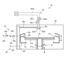
最初に、実施形態に係る基板処理システム1の概略構成について、図1を参照しながら説明する。図1は、実施形態に係る基板処理システム1の構成を示す模式平面図である。基板処理システム1は、めっき処理装置の一例である。
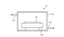
次に、めっき処理ユニット16の概略構成について、図2を参照しながら説明する。図2は、実施形態に係るめっき処理ユニット16の構成を示す模式断面図である。めっき処理ユニット16は、たとえば、ウェハWを1枚ずつ処理する枚葉式の処理ユニットとして構成される。
次に、熱処理ユニット17の概略構成について、図3を参照しながら説明する。図3は、実施形態に係る熱処理ユニット17の構成を示す模式断面図である。熱処理ユニット17は、たとえば、ウェハWを1枚ずつ処理する枚葉式の処理ユニットとして構成される。
つづいて、実施形態に係るめっき処理の詳細について、図4~図6を参照しながら説明する。図4は、実施形態に係るめっき処理前のウェハW表面の状態を示す拡大断面図である。
つづいて、実施形態の各種変形例について、図7~図9を参照しながら説明する。図7および図8は、実施形態の変形例1に係るめっき処理方法を説明するための図である。
図9は、実施形態の変形例2に係るめっき処理方法を説明するための図である。図9に示す変形例2では、薬液供給部32の構成が上述の実施形態および変形例1とは異なる。
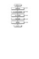
つづいて、図10および図11を参照しながら、実施形態に係る基板処理システム1が実行するめっき処理の詳細について説明する。図10は、実施形態に係るめっき処理の処理手順を示すフローチャートである。
5 制御部
16 めっき処理ユニット
31 基板保持部
32 薬液供給部
32d1 第1のノズル
32d2 第2のノズル
32d3 混合ノズル
L1 第1の薬液
L2 第2の薬液
M めっき液
W ウェハ(基板の一例)
Claims (9)
- 基板を準備する準備工程と、
金属イオン、還元剤および錯化剤を含有する第1の薬液と、アルカリ性を有する水溶液であるアルカリ水溶液を80(体積%)以上含む第2の薬液とを混合してめっき液を生成するめっき液生成工程と、
前記めっき液生成工程で前記めっき液を生成した直後に、生成された前記めっき液を用いて前記基板に対して無電解めっき処理を行うめっき処理工程と、
を含むめっき処理方法。 - 前記めっき液生成工程は、前記第1の薬液を第1のノズルで前記基板に吐出するとともに、前記第2の薬液を第2のノズルで前記基板に吐出して、前記基板上で前記第1の薬液と前記第2の薬液とを混合することにより行われる
請求項1に記載のめっき処理方法。 - 前記めっき液生成工程は、前記第2の薬液の液膜が形成された前記基板に対して、前記第1の薬液を前記基板に吐出することにより行われる
請求項1に記載のめっき処理方法。 - 前記めっき液生成工程は、前記第1の薬液と前記第2の薬液とを混合ノズル内で混合することにより行われる
請求項1に記載のめっき処理方法。 - 前記第2の薬液は、前記第1の薬液のpHが大きくなるようにpHを調整する
請求項1~4のいずれか一つに記載のめっき処理方法。 - 前記第2の薬液は、前記アルカリ水溶液および不可避的不純物からなる
請求項5に記載のめっき処理方法。 - 前記めっき液生成工程は、前記第1の薬液および前記第2の薬液のうち少なくとも一方を室温より高い温度に昇温した後に行われる
請求項1~6のいずれか一つに記載のめっき処理方法。 - 前記めっき液生成工程の前に行われ、前記金属イオンを含む第3の薬液と、前記還元剤を含む第4の薬液とを混合して前記第1の薬液を生成する第1薬液生成工程、をさらに含む
請求項1~7のいずれか一つに記載のめっき処理方法。 - 基板を保持する基板保持部と、
前記基板に薬液を供給する薬液供給部と、
各部を制御する制御部と、
を備え、
前記制御部は、
前記基板保持部で前記基板を保持し、
前記薬液供給部を制御して、金属イオン、還元剤および錯化剤を含有する第1の薬液と、アルカリ性を有する水溶液であるアルカリ水溶液を80(体積%)以上含む第2の薬液とを混合してめっき液を生成し、
前記めっき液を生成した直後に、生成された前記めっき液を用いて前記基板に対して無電解めっき処理を行う
めっき処理装置。
Applications Claiming Priority (3)
| Application Number | Priority Date | Filing Date | Title |
|---|---|---|---|
| JP2021005548 | 2021-01-18 | ||
| JP2021005548 | 2021-01-18 | ||
| PCT/JP2022/000191 WO2022153914A1 (ja) | 2021-01-18 | 2022-01-06 | めっき処理方法およびめっき処理装置 |
Publications (2)
| Publication Number | Publication Date |
|---|---|
| JPWO2022153914A1 JPWO2022153914A1 (ja) | 2022-07-21 |
| JP7614232B2 true JP7614232B2 (ja) | 2025-01-15 |
Family
ID=82447320
Family Applications (1)
| Application Number | Title | Priority Date | Filing Date |
|---|---|---|---|
| JP2022575552A Active JP7614232B2 (ja) | 2021-01-18 | 2022-01-06 | めっき処理方法およびめっき処理装置 |
Country Status (4)
| Country | Link |
|---|---|
| US (1) | US20240079269A1 (ja) |
| JP (1) | JP7614232B2 (ja) |
| KR (1) | KR20230129541A (ja) |
| WO (1) | WO2022153914A1 (ja) |
Families Citing this family (1)
| Publication number | Priority date | Publication date | Assignee | Title |
|---|---|---|---|---|
| JP2024130021A (ja) * | 2023-03-14 | 2024-09-30 | 株式会社Screenホールディングス | 基板処理方法および基板処理装置 |
Citations (6)
| Publication number | Priority date | Publication date | Assignee | Title |
|---|---|---|---|---|
| JP2004346399A (ja) | 2003-05-23 | 2004-12-09 | Ebara Corp | 基板処理方法及び基板処理装置 |
| JP2005097736A (ja) | 2003-08-27 | 2005-04-14 | Freescale Semiconductor Inc | 銅を覆う障壁物質を形成するための半導体処理方法及び組成物 |
| JP2006111938A (ja) | 2004-10-15 | 2006-04-27 | Tokyo Electron Ltd | 無電解めっき装置 |
| JP2013253282A (ja) | 2012-06-06 | 2013-12-19 | Kanto Gakuin | 無電解めっき浴および無電解めっき膜 |
| WO2019239772A1 (ja) | 2018-06-13 | 2019-12-19 | 株式会社Screenホールディングス | 無電解めっき方法、無電解めっき装置およびプログラム |
| WO2020137652A1 (ja) | 2018-12-28 | 2020-07-02 | 東京エレクトロン株式会社 | 基板液処理装置及び基板液処理方法 |
Family Cites Families (3)
| Publication number | Priority date | Publication date | Assignee | Title |
|---|---|---|---|---|
| JPH07197267A (ja) * | 1994-01-05 | 1995-08-01 | Nisshinbo Ind Inc | 無電解メッキ浴液調合装置 |
| US20050227074A1 (en) * | 2004-04-08 | 2005-10-13 | Masaaki Oyamada | Conductive electrolessly plated powder and method for making same |
| TWI833730B (zh) | 2018-02-21 | 2024-03-01 | 日商東京威力科創股份有限公司 | 多層配線之形成方法及記憶媒體 |
-
2022
- 2022-01-06 KR KR1020237027600A patent/KR20230129541A/ko active Pending
- 2022-01-06 US US18/261,157 patent/US20240079269A1/en active Pending
- 2022-01-06 JP JP2022575552A patent/JP7614232B2/ja active Active
- 2022-01-06 WO PCT/JP2022/000191 patent/WO2022153914A1/ja not_active Ceased
Patent Citations (6)
| Publication number | Priority date | Publication date | Assignee | Title |
|---|---|---|---|---|
| JP2004346399A (ja) | 2003-05-23 | 2004-12-09 | Ebara Corp | 基板処理方法及び基板処理装置 |
| JP2005097736A (ja) | 2003-08-27 | 2005-04-14 | Freescale Semiconductor Inc | 銅を覆う障壁物質を形成するための半導体処理方法及び組成物 |
| JP2006111938A (ja) | 2004-10-15 | 2006-04-27 | Tokyo Electron Ltd | 無電解めっき装置 |
| JP2013253282A (ja) | 2012-06-06 | 2013-12-19 | Kanto Gakuin | 無電解めっき浴および無電解めっき膜 |
| WO2019239772A1 (ja) | 2018-06-13 | 2019-12-19 | 株式会社Screenホールディングス | 無電解めっき方法、無電解めっき装置およびプログラム |
| WO2020137652A1 (ja) | 2018-12-28 | 2020-07-02 | 東京エレクトロン株式会社 | 基板液処理装置及び基板液処理方法 |
Also Published As
| Publication number | Publication date |
|---|---|
| US20240079269A1 (en) | 2024-03-07 |
| WO2022153914A1 (ja) | 2022-07-21 |
| KR20230129541A (ko) | 2023-09-08 |
| JPWO2022153914A1 (ja) | 2022-07-21 |
| TW202242969A (zh) | 2022-11-01 |
Similar Documents
| Publication | Publication Date | Title |
|---|---|---|
| JP6903171B2 (ja) | 多層配線の形成方法および記憶媒体 | |
| JP6910528B2 (ja) | 多層配線の形成方法および記憶媒体 | |
| JP7614232B2 (ja) | めっき処理方法およびめっき処理装置 | |
| TWI906450B (zh) | 鍍膜處理方法及鍍膜處理裝置 | |
| WO2012102062A1 (ja) | めっき処理装置、めっき処理方法および記録媒体 | |
| US10892176B2 (en) | Substrate processing apparatus having top plate with through hole and substrate processing method | |
| JP2022143230A (ja) | 基板処理方法および基板処理装置 | |
| US11795546B2 (en) | Substrate liquid processing apparatus, substrate liquid processing method and recording medium | |
| KR20220148247A (ko) | 기판 처리 장치 및 기판 처리 방법 | |
| WO2012102098A1 (ja) | めっき処理装置、めっき処理方法および記憶媒体 | |
| KR102745887B1 (ko) | 기판 처리 장치, 기판 처리 방법 및 기억매체 | |
| KR102745382B1 (ko) | 기판 처리 장치, 기판 처리 방법 및 기억매체 | |
| JP7221414B2 (ja) | 基板液処理方法および基板液処理装置 | |
| CN113227453B (zh) | 基板液处理装置和基板液处理方法 | |
| WO2024252965A1 (ja) | 基板処理方法、基板処理装置および記憶媒体 | |
| JP7657245B2 (ja) | めっき処理方法およびめっき処理装置 | |
| JP7467264B2 (ja) | 基板処理装置、基板処理方法およびノズル | |
| TW202444963A (zh) | 鍍敷處理方法及鍍敷處理裝置 | |
| WO2024009762A1 (ja) | 基板液処理方法及び基板液処理装置 | |
| KR20220136385A (ko) | 기판 처리 방법 및 기판 처리 장치 |
Legal Events
| Date | Code | Title | Description |
|---|---|---|---|
| A621 | Written request for application examination |
Free format text: JAPANESE INTERMEDIATE CODE: A621 Effective date: 20230710 |
|
| A131 | Notification of reasons for refusal |
Free format text: JAPANESE INTERMEDIATE CODE: A131 Effective date: 20240514 |
|
| A521 | Request for written amendment filed |
Free format text: JAPANESE INTERMEDIATE CODE: A523 Effective date: 20240627 |
|
| A131 | Notification of reasons for refusal |
Free format text: JAPANESE INTERMEDIATE CODE: A131 Effective date: 20240910 |
|
| A521 | Request for written amendment filed |
Free format text: JAPANESE INTERMEDIATE CODE: A523 Effective date: 20241011 |
|
| TRDD | Decision of grant or rejection written | ||
| A01 | Written decision to grant a patent or to grant a registration (utility model) |
Free format text: JAPANESE INTERMEDIATE CODE: A01 Effective date: 20241203 |
|
| A61 | First payment of annual fees (during grant procedure) |
Free format text: JAPANESE INTERMEDIATE CODE: A61 Effective date: 20241226 |
|
| R150 | Certificate of patent or registration of utility model |
Ref document number: 7614232 Country of ref document: JP Free format text: JAPANESE INTERMEDIATE CODE: R150 |