JP7586891B2 - 曲面表示パネル及び曲面表示装置 - Google Patents
曲面表示パネル及び曲面表示装置 Download PDFInfo
- Publication number
- JP7586891B2 JP7586891B2 JP2022502957A JP2022502957A JP7586891B2 JP 7586891 B2 JP7586891 B2 JP 7586891B2 JP 2022502957 A JP2022502957 A JP 2022502957A JP 2022502957 A JP2022502957 A JP 2022502957A JP 7586891 B2 JP7586891 B2 JP 7586891B2
- Authority
- JP
- Japan
- Prior art keywords
- midline
- display panel
- display area
- curved
- black matrix
- Prior art date
- Legal status (The legal status is an assumption and is not a legal conclusion. Google has not performed a legal analysis and makes no representation as to the accuracy of the status listed.)
- Active
Links
Images


Classifications
-
- G—PHYSICS
- G02—OPTICS
- G02F—OPTICAL DEVICES OR ARRANGEMENTS FOR THE CONTROL OF LIGHT BY MODIFICATION OF THE OPTICAL PROPERTIES OF THE MEDIA OF THE ELEMENTS INVOLVED THEREIN; NON-LINEAR OPTICS; FREQUENCY-CHANGING OF LIGHT; OPTICAL LOGIC ELEMENTS; OPTICAL ANALOGUE/DIGITAL CONVERTERS
- G02F1/00—Devices or arrangements for the control of the intensity, colour, phase, polarisation or direction of light arriving from an independent light source, e.g. switching, gating or modulating; Non-linear optics
- G02F1/01—Devices or arrangements for the control of the intensity, colour, phase, polarisation or direction of light arriving from an independent light source, e.g. switching, gating or modulating; Non-linear optics for the control of the intensity, phase, polarisation or colour
- G02F1/13—Devices or arrangements for the control of the intensity, colour, phase, polarisation or direction of light arriving from an independent light source, e.g. switching, gating or modulating; Non-linear optics for the control of the intensity, phase, polarisation or colour based on liquid crystals, e.g. single liquid crystal display cells
- G02F1/133—Constructional arrangements; Operation of liquid crystal cells; Circuit arrangements
- G02F1/1333—Constructional arrangements; Manufacturing methods
- G02F1/133305—Flexible substrates, e.g. plastics, organic film
-
- G—PHYSICS
- G02—OPTICS
- G02F—OPTICAL DEVICES OR ARRANGEMENTS FOR THE CONTROL OF LIGHT BY MODIFICATION OF THE OPTICAL PROPERTIES OF THE MEDIA OF THE ELEMENTS INVOLVED THEREIN; NON-LINEAR OPTICS; FREQUENCY-CHANGING OF LIGHT; OPTICAL LOGIC ELEMENTS; OPTICAL ANALOGUE/DIGITAL CONVERTERS
- G02F1/00—Devices or arrangements for the control of the intensity, colour, phase, polarisation or direction of light arriving from an independent light source, e.g. switching, gating or modulating; Non-linear optics
- G02F1/01—Devices or arrangements for the control of the intensity, colour, phase, polarisation or direction of light arriving from an independent light source, e.g. switching, gating or modulating; Non-linear optics for the control of the intensity, phase, polarisation or colour
- G02F1/13—Devices or arrangements for the control of the intensity, colour, phase, polarisation or direction of light arriving from an independent light source, e.g. switching, gating or modulating; Non-linear optics for the control of the intensity, phase, polarisation or colour based on liquid crystals, e.g. single liquid crystal display cells
- G02F1/133—Constructional arrangements; Operation of liquid crystal cells; Circuit arrangements
- G02F1/1333—Constructional arrangements; Manufacturing methods
- G02F1/1335—Structural association of cells with optical devices, e.g. polarisers or reflectors
- G02F1/133509—Filters, e.g. light shielding masks
- G02F1/133512—Light shielding layers, e.g. black matrix
-
- G—PHYSICS
- G02—OPTICS
- G02F—OPTICAL DEVICES OR ARRANGEMENTS FOR THE CONTROL OF LIGHT BY MODIFICATION OF THE OPTICAL PROPERTIES OF THE MEDIA OF THE ELEMENTS INVOLVED THEREIN; NON-LINEAR OPTICS; FREQUENCY-CHANGING OF LIGHT; OPTICAL LOGIC ELEMENTS; OPTICAL ANALOGUE/DIGITAL CONVERTERS
- G02F1/00—Devices or arrangements for the control of the intensity, colour, phase, polarisation or direction of light arriving from an independent light source, e.g. switching, gating or modulating; Non-linear optics
- G02F1/01—Devices or arrangements for the control of the intensity, colour, phase, polarisation or direction of light arriving from an independent light source, e.g. switching, gating or modulating; Non-linear optics for the control of the intensity, phase, polarisation or colour
- G02F1/13—Devices or arrangements for the control of the intensity, colour, phase, polarisation or direction of light arriving from an independent light source, e.g. switching, gating or modulating; Non-linear optics for the control of the intensity, phase, polarisation or colour based on liquid crystals, e.g. single liquid crystal display cells
- G02F1/133—Constructional arrangements; Operation of liquid crystal cells; Circuit arrangements
- G02F1/1333—Constructional arrangements; Manufacturing methods
- G02F1/133388—Constructional arrangements; Manufacturing methods with constructional differences between the display region and the peripheral region
-
- G—PHYSICS
- G02—OPTICS
- G02F—OPTICAL DEVICES OR ARRANGEMENTS FOR THE CONTROL OF LIGHT BY MODIFICATION OF THE OPTICAL PROPERTIES OF THE MEDIA OF THE ELEMENTS INVOLVED THEREIN; NON-LINEAR OPTICS; FREQUENCY-CHANGING OF LIGHT; OPTICAL LOGIC ELEMENTS; OPTICAL ANALOGUE/DIGITAL CONVERTERS
- G02F1/00—Devices or arrangements for the control of the intensity, colour, phase, polarisation or direction of light arriving from an independent light source, e.g. switching, gating or modulating; Non-linear optics
- G02F1/01—Devices or arrangements for the control of the intensity, colour, phase, polarisation or direction of light arriving from an independent light source, e.g. switching, gating or modulating; Non-linear optics for the control of the intensity, phase, polarisation or colour
- G02F1/13—Devices or arrangements for the control of the intensity, colour, phase, polarisation or direction of light arriving from an independent light source, e.g. switching, gating or modulating; Non-linear optics for the control of the intensity, phase, polarisation or colour based on liquid crystals, e.g. single liquid crystal display cells
- G02F1/133—Constructional arrangements; Operation of liquid crystal cells; Circuit arrangements
- G02F1/1333—Constructional arrangements; Manufacturing methods
- G02F1/133391—Constructional arrangement for sub-divided displays
-
- G—PHYSICS
- G02—OPTICS
- G02F—OPTICAL DEVICES OR ARRANGEMENTS FOR THE CONTROL OF LIGHT BY MODIFICATION OF THE OPTICAL PROPERTIES OF THE MEDIA OF THE ELEMENTS INVOLVED THEREIN; NON-LINEAR OPTICS; FREQUENCY-CHANGING OF LIGHT; OPTICAL LOGIC ELEMENTS; OPTICAL ANALOGUE/DIGITAL CONVERTERS
- G02F1/00—Devices or arrangements for the control of the intensity, colour, phase, polarisation or direction of light arriving from an independent light source, e.g. switching, gating or modulating; Non-linear optics
- G02F1/01—Devices or arrangements for the control of the intensity, colour, phase, polarisation or direction of light arriving from an independent light source, e.g. switching, gating or modulating; Non-linear optics for the control of the intensity, phase, polarisation or colour
- G02F1/13—Devices or arrangements for the control of the intensity, colour, phase, polarisation or direction of light arriving from an independent light source, e.g. switching, gating or modulating; Non-linear optics for the control of the intensity, phase, polarisation or colour based on liquid crystals, e.g. single liquid crystal display cells
- G02F1/133—Constructional arrangements; Operation of liquid crystal cells; Circuit arrangements
- G02F1/1333—Constructional arrangements; Manufacturing methods
- G02F1/1335—Structural association of cells with optical devices, e.g. polarisers or reflectors
- G02F1/133509—Filters, e.g. light shielding masks
- G02F1/133514—Colour filters
-
- G—PHYSICS
- G02—OPTICS
- G02F—OPTICAL DEVICES OR ARRANGEMENTS FOR THE CONTROL OF LIGHT BY MODIFICATION OF THE OPTICAL PROPERTIES OF THE MEDIA OF THE ELEMENTS INVOLVED THEREIN; NON-LINEAR OPTICS; FREQUENCY-CHANGING OF LIGHT; OPTICAL LOGIC ELEMENTS; OPTICAL ANALOGUE/DIGITAL CONVERTERS
- G02F1/00—Devices or arrangements for the control of the intensity, colour, phase, polarisation or direction of light arriving from an independent light source, e.g. switching, gating or modulating; Non-linear optics
- G02F1/01—Devices or arrangements for the control of the intensity, colour, phase, polarisation or direction of light arriving from an independent light source, e.g. switching, gating or modulating; Non-linear optics for the control of the intensity, phase, polarisation or colour
- G02F1/13—Devices or arrangements for the control of the intensity, colour, phase, polarisation or direction of light arriving from an independent light source, e.g. switching, gating or modulating; Non-linear optics for the control of the intensity, phase, polarisation or colour based on liquid crystals, e.g. single liquid crystal display cells
- G02F1/133—Constructional arrangements; Operation of liquid crystal cells; Circuit arrangements
- G02F1/136—Liquid crystal cells structurally associated with a semi-conducting layer or substrate, e.g. cells forming part of an integrated circuit
- G02F1/1362—Active matrix addressed cells
- G02F1/136209—Light shielding layers, e.g. black matrix, incorporated in the active matrix substrate, e.g. structurally associated with the switching element
-
- G—PHYSICS
- G02—OPTICS
- G02F—OPTICAL DEVICES OR ARRANGEMENTS FOR THE CONTROL OF LIGHT BY MODIFICATION OF THE OPTICAL PROPERTIES OF THE MEDIA OF THE ELEMENTS INVOLVED THEREIN; NON-LINEAR OPTICS; FREQUENCY-CHANGING OF LIGHT; OPTICAL LOGIC ELEMENTS; OPTICAL ANALOGUE/DIGITAL CONVERTERS
- G02F1/00—Devices or arrangements for the control of the intensity, colour, phase, polarisation or direction of light arriving from an independent light source, e.g. switching, gating or modulating; Non-linear optics
- G02F1/01—Devices or arrangements for the control of the intensity, colour, phase, polarisation or direction of light arriving from an independent light source, e.g. switching, gating or modulating; Non-linear optics for the control of the intensity, phase, polarisation or colour
- G02F1/13—Devices or arrangements for the control of the intensity, colour, phase, polarisation or direction of light arriving from an independent light source, e.g. switching, gating or modulating; Non-linear optics for the control of the intensity, phase, polarisation or colour based on liquid crystals, e.g. single liquid crystal display cells
- G02F1/133—Constructional arrangements; Operation of liquid crystal cells; Circuit arrangements
- G02F1/136—Liquid crystal cells structurally associated with a semi-conducting layer or substrate, e.g. cells forming part of an integrated circuit
- G02F1/1362—Active matrix addressed cells
- G02F1/136286—Wiring, e.g. gate line, drain line
-
- G—PHYSICS
- G09—EDUCATION; CRYPTOGRAPHY; DISPLAY; ADVERTISING; SEALS
- G09F—DISPLAYING; ADVERTISING; SIGNS; LABELS OR NAME-PLATES; SEALS
- G09F9/00—Indicating arrangements for variable information in which the information is built-up on a support by selection or combination of individual elements
- G09F9/30—Indicating arrangements for variable information in which the information is built-up on a support by selection or combination of individual elements in which the desired character or characters are formed by combining individual elements
- G09F9/301—Indicating arrangements for variable information in which the information is built-up on a support by selection or combination of individual elements in which the desired character or characters are formed by combining individual elements flexible foldable or roll-able electronic displays, e.g. thin LCD, OLED
-
- G—PHYSICS
- G02—OPTICS
- G02F—OPTICAL DEVICES OR ARRANGEMENTS FOR THE CONTROL OF LIGHT BY MODIFICATION OF THE OPTICAL PROPERTIES OF THE MEDIA OF THE ELEMENTS INVOLVED THEREIN; NON-LINEAR OPTICS; FREQUENCY-CHANGING OF LIGHT; OPTICAL LOGIC ELEMENTS; OPTICAL ANALOGUE/DIGITAL CONVERTERS
- G02F2201/00—Constructional arrangements not provided for in groups G02F1/00 - G02F7/00
- G02F2201/40—Arrangements for improving the aperture ratio
Landscapes
- Physics & Mathematics (AREA)
- Nonlinear Science (AREA)
- General Physics & Mathematics (AREA)
- Optics & Photonics (AREA)
- Crystallography & Structural Chemistry (AREA)
- Chemical & Material Sciences (AREA)
- Mathematical Physics (AREA)
- Engineering & Computer Science (AREA)
- Microelectronics & Electronic Packaging (AREA)
- Theoretical Computer Science (AREA)
- Devices For Indicating Variable Information By Combining Individual Elements (AREA)
- Liquid Crystal (AREA)
- Electroluminescent Light Sources (AREA)
Description
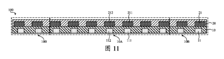
中線と、前記中線に対して対称に設けられる中心表示区域と、を有し、
前記中線から離れる側から前記中線に向かう方向において、前記中心表示区域に位置する前記サブ画素の開口率は、徐々に大きくなり、隣接する二つの前記サブ画素の開口率の差は、2%以下である、
曲面表示パネルが提供される。
前記中心表示区域の背向する両側に位置するように前記中線に対して対称に設けられる非中心表示区域をさらに含み、
前記中線から離れる側から前記中線に向かう方向において、前記非中心表示区域に位置する前記サブ画素の開口率は、徐々に大きくなり、前記非中心表示区域及び前記中心表示区域において隣接するいずれかの二つの前記サブ画素の開口率の差は、いずれも2%以下である。
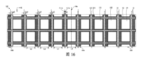
第1方向に沿って延在し、かつ第2方向に沿って配列される複数本のデータ線を含むアレイ基板であって、複数本の前記データ線が前記第1方向に沿って延在する第1中心線をそれぞれ有する複数本の第1データ線を含むアレイ基板と、
前記アレイ基板に対向して設けられ、前記第1方向に沿って延在する第2中心線をそれぞれ有する複数の第1ブラックマトリクス部を含むカラーフィルム基板であって、単一の前記第1ブラックマトリクス部がこれと対応する単一の前記第1データ線を覆うカラーフィルム基板と、をさらに含み、
前記中線は、前記第1方向に沿って延在し、少なくとも四本の前記第1データ線は、前記中心表示区域に位置するように前記中線に対して対称に設けられ、
前記曲面表示パネルが湾曲しない場合に、前記中心表示区域において、前記第1中心線と、これと対応する前記第2中心線とは、前記第2方向において第1所定距離を有し、前記中線から離れる側から前記中線に向かう方向において、前記第1所定距離は、徐々に小さくなる。
前記曲面表示パネルが湾曲しない場合に、前記中線から離れる側から前記中線に向かう方向において、前記中心表示区域において隣接する二つの前記第1ブラックマトリクス部の間の距離は、徐々に大きくなる。
前記カラーフィルム基板は、前記第1方向に沿って延在し、かつ前記第3中心線との間の前記第2方向における距離がゼロである第4中心線を有する第2ブラックマトリクス部をさらに含む。
前記第2方向において、前記第2ブラックマトリクス部と隣接する前記第1ブラックマトリクス部との間には、隣接する二つの前記第1ブラックマトリクス部の間の距離よりも大きい中心距離があり、
前記中線から離れる側から前記中線に向かう方向において、隣接する二つの前記第1ブラックマトリクス部の間の距離は、徐々に大きくなる。
前記第2方向において、前記中線に隣接する二つの前記第1ブラックマトリクス部の間には、前記中線から前記中線を離れる方向において隣接する二つの前記第1ブラックマトリクス部の間の距離よりも大きい中心距離があり、
前記中線から離れる側から前記中線に向かう方向において、隣接する二つの前記第1ブラックマトリクス部の間の距離は、徐々に大きくなる。
前記中線から前記中線を離れる方向において、前記第1所定距離は、等差数列に構成される。
前記中心表示区域の背向する両側に位置するように前記中線に対して対称に設けられる非中心表示区域を、さらに含み、
前記非中心表示区域において、前記第1中心線と、これと対応する前記第2中心線との間には、前記第2方向において前記第1所定距離よりも大きい第2所定距離があり、
前記中線から離れる側から前記中線に向かう方向において、前記第2所定距離は、徐々に小さくなる。
同時に前記中心表示区域及び前記非中心表示区域に位置する複数のサブ画素を含み、
前記中線から離れる側から前記中線に向かう方向において、前記サブ画素の開口率は、等差数列に構成される。
前記中心表示区域の背向する両側に位置するように前記中線に対して対称に設けられる非中心表示区域を、さらに含み、
前記非中心表示区域において、前記第1中心線と、これと対応する前記第2中心線との間には、前記第2方向において前記第1所定距離よりも大きい第2所定距離があり、
前記中線から離れる側から前記中線に向かう方向において、前記第2所定距離は、不変である。
前記中心表示区域に位置する複数の第1サブ画素と、
前記非中心表示区域に位置する複数の第2サブ画素と、を含み、
前記中線から離れる側から前記中線に向かう方向において、前記第1サブ画素の開口率は、等差数列に構成され、前記第2サブ画素の開口率は、同一である。
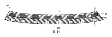
前記曲面表示パネルが湾曲する場合に、前記第1中心線と、これと対応する前記第2中心線との間の前記第2方向における距離は、ゼロである。
第1方向に沿って延在し、かつ第2方向に沿って配列される複数本のデータ線を含むアレイ基板であって、複数本の前記データ線が前記第1方向に沿って延在する第1中心線をそれぞれ有する複数本の第1データ線を含むアレイ基板と、
前記アレイ基板に対向して設けられ、前記第1方向に沿って延在する第2中心線をそれぞれ有する複数の第1ブラックマトリクス部を含むカラーフィルム基板であって、単一の前記第1ブラックマトリクス部がこれと対応する単一の前記第1データ線を覆うカラーフィルム基板と、をさらに含み、
前記曲面表示パネルは、前記第1方向に沿って延在する中線と、前記中線に対して対称に設けられる中心表示区域と、前記中心表示区域の背向する両側に位置するように前記中線に対して対称に設けられる非中心表示区域と、を有し、
少なくとも四本の前記第1データ線は、前記中心表示区域に位置するように前記中線に対して対称に設けられ、
前記曲面表示パネルが湾曲した場合に、前記中線から離れる側から前記中線に向かう方向において、前記中心表示区域に位置する前記サブ画素の開口率は、徐々に大きくなり、隣接する二つの前記サブ画素の開口率の差は、2%以下であり、
前記中線から離れる側から前記中線に向かう方向において、前記非中心表示区域に位置する前記サブ画素の開口率は、徐々に大きくなり、前記非中心表示区域及び前記中心表示区域において隣接するいずれかの二つの前記サブ画素の開口率の差は、いずれも2%以下で、
前記曲面表示パネルが湾曲しない場合に、前記中心表示区域において、前記第1中心線と、これと対応する前記第2中心線とは、前記第2方向において第1所定距離を有し、前記中線から離れる側から前記中線に向かう方向において、前記第1所定距離は、徐々に小さくなる、
曲面表示パネルがさらに提供される。
前記曲面表示パネルは、
複数のサブ画素と、中線と、前記中線に対して対称に設けられる中心表示区域と、を含み、
前記中線から離れる側から前記中線に向かう方向において、前記中心表示区域に位置する前記サブ画素の開口率は、徐々に大きくなり、隣接する二つの前記サブ画素の開口率の差は、2%以下である曲面表示装置をさらに提供される。
前記中心表示区域の背向する両側に位置するように前記中線に対して対称に設けられる非中心表示区域をさらに含み、
前記中線から離れる側から前記中線に向かう方向において、前記非中心表示区域に位置する前記サブ画素の開口率は、徐々に大きくなり、前記非中心表示区域及び前記中心表示区域において隣接するいずれかの二つの前記サブ画素の開口率の差は、いずれも2%以下である。
第1方向に沿って延在し、かつ第2方向に沿って配列される複数本のデータ線を含むアレイ基板であって、複数本の前記データ線が前記第1方向に沿って延在する第1中心線をそれぞれ有する複数本の第1データ線を含むアレイ基板と、
前記アレイ基板に対向して設けられ、前記第1方向に沿って延在する第2中心線をそれぞれ有する複数の第1ブラックマトリクス部を含むカラーフィルム基板であって、単一の前記第1ブラックマトリクス部がこれと対応する単一の前記第1データ線を覆うカラーフィルム基板と、をさらに含み、
前記中線は、前記第1方向に沿って延在し、少なくとも四本の前記第1データ線は、前記中心表示区域に位置するように前記中線に対して対称に設けられ、
前記曲面表示パネルが湾曲しない場合に、前記中心表示区域において、前記第1中心線と、これと対応する前記第2中心線とは、前記第2方向において第1所定距離を有し、前記中線から離れる側から前記中線に向かう方向において、前記第1所定距離は、徐々に小さくなる。
前記曲面表示パネルが湾曲しない場合に、前記中線から離れる側から前記中線に向かう方向において、前記中心表示区域において隣接する二つの前記第1ブラックマトリクス部の間の距離は、徐々に大きくなる。
前記カラーフィルム基板は、前記第1方向に沿って延在し、かつ前記第3中心線との間の前記第2方向における距離がゼロである第4中心線を有する第2ブラックマトリクス部をさらに含む。
Claims (10)
- 複数のサブ画素を含む曲面表示パネルであって、
中線と、前記中線に対して対称に設けられる中心表示区域と、を有し、
前記中線から離れる側から前記中線に向かう方向において、前記中心表示区域に位置する前記サブ画素の開口率は、徐々に大きくなり、隣接する二つの前記サブ画素の開口率の差は、2%以下であり、
第1方向に沿って延在し、かつ第2方向に沿って配列される複数本のデータ線を含むアレイ基板であって、複数本の前記データ線が前記第1方向に沿って延在する第1中心線をそれぞれ有する複数本の第1データ線を含むアレイ基板と、
前記アレイ基板に対向して設けられ、前記第1方向に沿って延在する第2中心線をそれぞれ有する複数の第1ブラックマトリクス部を含むカラーフィルム基板であって、単一の前記第1ブラックマトリクス部がこれと対応する単一の前記第1データ線を覆うカラーフィルム基板と、をさらに含み、
前記中線は、前記第1方向に沿って延在し、少なくとも四本の前記第1データ線は、前記中心表示区域に位置するように前記中線に対して対称に設けられ、
前記曲面表示パネルが湾曲しない場合に、前記中心表示区域において、前記第1中心線と、これと対応する前記第2中心線とは、前記第2方向において第1所定距離を有し、前記中線から離れる側から前記中線に向かう方向において、前記第1所定距離は、徐々に小さくなり、
前記中心表示区域の背向する両側に位置するように前記中線に対して対称に設けられる非中心表示区域を、さらに含み、
前記非中心表示区域において、前記第1中心線と、これと対応する前記第2中心線との間には、前記第2方向において前記第1所定距離よりも大きい第2所定距離があり、
前記中線から離れる側から前記中線に向かう方向において、前記第2所定距離は、不変である、
曲面表示パネル。 - 前記中線から離れる側から前記中線に向かう方向において、前記非中心表示区域に位置する前記サブ画素の開口率は、徐々に大きくなり、前記非中心表示区域及び前記中心表示区域において隣接するいずれかの二つの前記サブ画素の開口率の差は、いずれも2%以下である、
請求項1に記載の曲面表示パネル。 - 少なくとも六本の前記第1データ線は、前記中心表示区域に位置し、
前記曲面表示パネルが湾曲しない場合に、前記中線から離れる側から前記中線に向かう方向において、前記中心表示区域において隣接する二つの前記第1ブラックマトリクス部の間の距離は、徐々に大きくなる、
請求項1に記載の曲面表示パネル。 - 複数本の前記データ線は、前記第1方向に沿って延在し、かつ前記中線との間の前記第2方向における距離がゼロである第3中心線を有する第2データ線をさらに含み、
前記カラーフィルム基板は、前記第1方向に沿って延在し、かつ前記第3中心線との間の前記第2方向における距離がゼロである第4中心線を有する第2ブラックマトリクス部をさらに含む、
請求項1に記載の曲面表示パネル。 - 隣接する二本の各前記データ線の間の距離は、等しく、
前記第2方向において、前記第2ブラックマトリクス部と隣接する前記第1ブラックマトリクス部との間には、隣接する二つの前記第1ブラックマトリクス部の間の距離よりも大きい中心距離があり、
前記中線から離れる側から前記中線に向かう方向において、隣接する二つの前記第1ブラックマトリクス部の間の距離は、徐々に大きくなる、
請求項4に記載の曲面表示パネル。 - 隣接する二本の各前記データ線の間の距離は、等しく、
前記第2方向において、前記中線に隣接する二つの前記第1ブラックマトリクス部の間には、前記中線から前記中線を離れる方向において隣接する二つの前記第1ブラックマトリクス部の間の距離よりも大きい中心距離があり、
前記中線から離れる側から前記中線に向かう方向において、隣接する二つの前記第1ブラックマトリクス部の間の距離は、徐々に大きくなる、
請求項1に記載の曲面表示パネル。 - 少なくとも六本の前記第1データ線は、前記中心表示区域に位置し、
前記中線から前記中線を離れる方向において、前記第1所定距離は、等差数列に構成される、
請求項1に記載の曲面表示パネル。 - 前記中心表示区域に位置する複数の第1サブ画素と、
前記非中心表示区域に位置する複数の第2サブ画素と、を含み、
前記中線から離れる側から前記中線に向かう方向において、前記第1サブ画素の開口率は、等差数列に構成され、前記第2サブ画素の開口率は、同一である、
請求項1に記載の曲面表示パネル。 - 前記曲面表示パネルが湾曲する場合に、前記第1中心線と、これと対応する前記第2中心線との間の前記第2方向における距離は、ゼロである、
請求項1に記載の曲面表示パネル。 - 請求項1~9のいずれか一項に記載の前記曲面表示パネルを含む、
曲面表示装置。
Applications Claiming Priority (3)
| Application Number | Priority Date | Filing Date | Title |
|---|---|---|---|
| CN202111646199.1 | 2021-12-30 | ||
| CN202111646199.1A CN114326191B (zh) | 2021-12-30 | 2021-12-30 | 曲面显示面板及曲面显示装置 |
| PCT/CN2022/071272 WO2023123554A1 (zh) | 2021-12-30 | 2022-01-11 | 曲面显示面板及曲面显示装置 |
Publications (2)
| Publication Number | Publication Date |
|---|---|
| JP2024503949A JP2024503949A (ja) | 2024-01-30 |
| JP7586891B2 true JP7586891B2 (ja) | 2024-11-19 |
Family
ID=81016501
Family Applications (1)
| Application Number | Title | Priority Date | Filing Date |
|---|---|---|---|
| JP2022502957A Active JP7586891B2 (ja) | 2021-12-30 | 2022-01-11 | 曲面表示パネル及び曲面表示装置 |
Country Status (6)
| Country | Link |
|---|---|
| US (1) | US12130509B2 (ja) |
| EP (1) | EP4465122A4 (ja) |
| JP (1) | JP7586891B2 (ja) |
| KR (1) | KR102655951B1 (ja) |
| CN (1) | CN114326191B (ja) |
| WO (1) | WO2023123554A1 (ja) |
Families Citing this family (1)
| Publication number | Priority date | Publication date | Assignee | Title |
|---|---|---|---|---|
| CN114023202B (zh) * | 2021-10-26 | 2023-12-05 | 惠州华星光电显示有限公司 | 显示面板及显示终端 |
Citations (4)
| Publication number | Priority date | Publication date | Assignee | Title |
|---|---|---|---|---|
| US20150362796A1 (en) | 2014-06-13 | 2015-12-17 | Lg Display Co., Ltd. | Curved liquid crystal display device and color filter substrate for the same |
| US20150370121A1 (en) | 2014-06-23 | 2015-12-24 | Shenzhen China Star Optoelectronics Technology Co. Ltd. | Color filter substrates and liquid crystal devices having black matrixes with variable widths |
| US20160033815A1 (en) | 2014-08-01 | 2016-02-04 | Samsung Display Co., Ltd. | Display device |
| JP2017181818A (ja) | 2016-03-30 | 2017-10-05 | パナソニック液晶ディスプレイ株式会社 | 表示装置 |
Family Cites Families (19)
| Publication number | Priority date | Publication date | Assignee | Title |
|---|---|---|---|---|
| KR101030537B1 (ko) | 2004-06-30 | 2011-04-21 | 엘지디스플레이 주식회사 | 액정표시장치 및 그를 이용한 휘도 편차 보상방법 |
| JP5026777B2 (ja) | 2006-12-11 | 2012-09-19 | インフォビジョン オプトエレクトロニクス ホールデングズ リミティッド | 湾曲液晶パネル及び液晶表示装置 |
| JP5123078B2 (ja) | 2008-06-30 | 2013-01-16 | 三菱電機株式会社 | 液晶表示装置及び製造方法 |
| CN104007575A (zh) | 2014-06-18 | 2014-08-27 | 深圳市华星光电技术有限公司 | 黑矩阵不等宽的彩色滤光片基板及液晶显示器 |
| CN104076552B (zh) * | 2014-06-25 | 2016-08-24 | 深圳市华星光电技术有限公司 | 彩膜基板及曲面显示装置 |
| TWI571673B (zh) * | 2014-10-01 | 2017-02-21 | 友達光電股份有限公司 | 曲面顯示面板 |
| TWI639869B (zh) * | 2014-12-31 | 2018-11-01 | 友達光電股份有限公司 | 顯示面板 |
| CN104597671B (zh) * | 2015-01-22 | 2018-07-27 | 厦门天马微电子有限公司 | 阵列基板、显示面板及显示装置 |
| KR102354998B1 (ko) * | 2015-03-18 | 2022-01-24 | 삼성디스플레이 주식회사 | 액정 표시 장치 |
| CN105242439B (zh) * | 2015-11-18 | 2019-04-23 | 京东方科技集团股份有限公司 | 显示基板、显示面板以及显示装置 |
| KR102582176B1 (ko) * | 2016-02-05 | 2023-09-25 | 삼성디스플레이 주식회사 | 곡면 표시 장치 |
| CN105824161B (zh) * | 2016-05-25 | 2023-07-14 | 福州京东方光电科技有限公司 | 一种液晶显示面板及液晶显示装置 |
| KR102588089B1 (ko) * | 2016-07-29 | 2023-10-12 | 엘지디스플레이 주식회사 | 곡면형 표시장치 |
| CN107908038B (zh) * | 2017-11-28 | 2020-04-28 | 武汉天马微电子有限公司 | 一种曲面显示面板及其显示装置 |
| CN110501847B (zh) * | 2018-05-16 | 2022-06-14 | 群创光电股份有限公司 | 显示设备 |
| CN109445166A (zh) * | 2018-12-19 | 2019-03-08 | 武汉华星光电技术有限公司 | 一种显示面板及显示装置 |
| US11237425B2 (en) * | 2018-12-19 | 2022-02-01 | Wuhan China Star Optoelectronics Technology Co., Ltd. | Display panel and display device |
| CN109445159B (zh) * | 2018-12-27 | 2021-07-09 | 厦门天马微电子有限公司 | 柔性显示模组及其驱动方法、柔性显示装置 |
| CN111679489B (zh) * | 2020-06-30 | 2022-09-13 | 厦门天马微电子有限公司 | 一种曲面显示面板及其制备方法、显示装置 |
-
2021
- 2021-12-30 CN CN202111646199.1A patent/CN114326191B/zh active Active
-
2022
- 2022-01-11 KR KR1020227022328A patent/KR102655951B1/ko active Active
- 2022-01-11 JP JP2022502957A patent/JP7586891B2/ja active Active
- 2022-01-11 WO PCT/CN2022/071272 patent/WO2023123554A1/zh not_active Ceased
- 2022-01-11 US US17/597,951 patent/US12130509B2/en active Active
- 2022-01-11 EP EP22717055.2A patent/EP4465122A4/en active Pending
Patent Citations (4)
| Publication number | Priority date | Publication date | Assignee | Title |
|---|---|---|---|---|
| US20150362796A1 (en) | 2014-06-13 | 2015-12-17 | Lg Display Co., Ltd. | Curved liquid crystal display device and color filter substrate for the same |
| US20150370121A1 (en) | 2014-06-23 | 2015-12-24 | Shenzhen China Star Optoelectronics Technology Co. Ltd. | Color filter substrates and liquid crystal devices having black matrixes with variable widths |
| US20160033815A1 (en) | 2014-08-01 | 2016-02-04 | Samsung Display Co., Ltd. | Display device |
| JP2017181818A (ja) | 2016-03-30 | 2017-10-05 | パナソニック液晶ディスプレイ株式会社 | 表示装置 |
Also Published As
| Publication number | Publication date |
|---|---|
| KR20230106118A (ko) | 2023-07-12 |
| CN114326191A (zh) | 2022-04-12 |
| WO2023123554A1 (zh) | 2023-07-06 |
| CN114326191B (zh) | 2023-08-22 |
| EP4465122A1 (en) | 2024-11-20 |
| JP2024503949A (ja) | 2024-01-30 |
| KR102655951B1 (ko) | 2024-04-11 |
| EP4465122A4 (en) | 2026-01-14 |
| US12130509B2 (en) | 2024-10-29 |
| US20240036369A1 (en) | 2024-02-01 |
Similar Documents
| Publication | Publication Date | Title |
|---|---|---|
| US9858870B2 (en) | Pixel unit, pixel array and liquid crystal display panel | |
| US7259812B2 (en) | In plane switching mode liquid crystal display device having 4-pixel structure | |
| US20130070002A1 (en) | Display panel and display device | |
| EP3572867B1 (en) | Array substrate and display apparatus | |
| CN105096765A (zh) | 一种像素结构、显示面板及显示装置 | |
| JP5015250B2 (ja) | 液晶表示装置 | |
| WO2013127199A1 (zh) | Tft-lcd阵列基板及显示装置 | |
| AU2011272389B2 (en) | Display panel and display device | |
| CN111477113A (zh) | 一种透明显示面板及显示装置 | |
| CN110543039B (zh) | 显示面板和显示装置 | |
| WO2020073568A1 (zh) | 一种像素电极结构及显示装置 | |
| JP7586891B2 (ja) | 曲面表示パネル及び曲面表示装置 | |
| US10014323B2 (en) | Array substrate, curved display panel and curved display device | |
| US20160282680A1 (en) | Liquid crystal panels | |
| US9696579B2 (en) | Liquid crystal panel and liquid crystal displaying device | |
| US10365528B2 (en) | Array substrate, method of manufacturing the same, display panel and display device | |
| US11392001B2 (en) | Pixel structure and liquid crystal display panel | |
| US10712605B2 (en) | Liquid crystal display device | |
| US9857638B2 (en) | Display device | |
| US20070058126A1 (en) | Liquid crystal display panel and manufacturing method thereof | |
| EA044195B1 (ru) | Криволинейная дисплейная панель и криволинейное дисплейное устройство | |
| TW202601256A (zh) | 顯示面板 | |
| TW201822175A (zh) | 顯示面板 | |
| CN110989250A (zh) | 显示器 | |
| CN118033953A (zh) | 阵列基板、显示面板及显示设备 |
Legal Events
| Date | Code | Title | Description |
|---|---|---|---|
| A621 | Written request for application examination |
Free format text: JAPANESE INTERMEDIATE CODE: A621 Effective date: 20220304 |
|
| A131 | Notification of reasons for refusal |
Free format text: JAPANESE INTERMEDIATE CODE: A131 Effective date: 20240213 |
|
| A521 | Request for written amendment filed |
Free format text: JAPANESE INTERMEDIATE CODE: A523 Effective date: 20240508 |
|
| A02 | Decision of refusal |
Free format text: JAPANESE INTERMEDIATE CODE: A02 Effective date: 20240611 |
|
| A521 | Request for written amendment filed |
Free format text: JAPANESE INTERMEDIATE CODE: A523 Effective date: 20240830 |
|
| A911 | Transfer to examiner for re-examination before appeal (zenchi) |
Free format text: JAPANESE INTERMEDIATE CODE: A911 Effective date: 20240906 |
|
| TRDD | Decision of grant or rejection written | ||
| A01 | Written decision to grant a patent or to grant a registration (utility model) |
Free format text: JAPANESE INTERMEDIATE CODE: A01 Effective date: 20241029 |
|
| A61 | First payment of annual fees (during grant procedure) |
Free format text: JAPANESE INTERMEDIATE CODE: A61 Effective date: 20241107 |
|
| R150 | Certificate of patent or registration of utility model |
Ref document number: 7586891 Country of ref document: JP Free format text: JAPANESE INTERMEDIATE CODE: R150 |