JP7581396B2 - 調光フィルム - Google Patents
調光フィルム Download PDFInfo
- Publication number
- JP7581396B2 JP7581396B2 JP2023017382A JP2023017382A JP7581396B2 JP 7581396 B2 JP7581396 B2 JP 7581396B2 JP 2023017382 A JP2023017382 A JP 2023017382A JP 2023017382 A JP2023017382 A JP 2023017382A JP 7581396 B2 JP7581396 B2 JP 7581396B2
- Authority
- JP
- Japan
- Prior art keywords
- film
- layer
- electrode layer
- light
- resin
- Prior art date
- Legal status (The legal status is an assumption and is not a legal conclusion. Google has not performed a legal analysis and makes no representation as to the accuracy of the status listed.)
- Active
Links
Images


Classifications
-
- G—PHYSICS
- G02—OPTICS
- G02F—OPTICAL DEVICES OR ARRANGEMENTS FOR THE CONTROL OF LIGHT BY MODIFICATION OF THE OPTICAL PROPERTIES OF THE MEDIA OF THE ELEMENTS INVOLVED THEREIN; NON-LINEAR OPTICS; FREQUENCY-CHANGING OF LIGHT; OPTICAL LOGIC ELEMENTS; OPTICAL ANALOGUE/DIGITAL CONVERTERS
- G02F1/00—Devices or arrangements for the control of the intensity, colour, phase, polarisation or direction of light arriving from an independent light source, e.g. switching, gating or modulating; Non-linear optics
- G02F1/01—Devices or arrangements for the control of the intensity, colour, phase, polarisation or direction of light arriving from an independent light source, e.g. switching, gating or modulating; Non-linear optics for the control of the intensity, phase, polarisation or colour
- G02F1/13—Devices or arrangements for the control of the intensity, colour, phase, polarisation or direction of light arriving from an independent light source, e.g. switching, gating or modulating; Non-linear optics for the control of the intensity, phase, polarisation or colour based on liquid crystals, e.g. single liquid crystal display cells
- G02F1/133—Constructional arrangements; Operation of liquid crystal cells; Circuit arrangements
- G02F1/1333—Constructional arrangements; Manufacturing methods
- G02F1/1343—Electrodes
-
- G—PHYSICS
- G02—OPTICS
- G02F—OPTICAL DEVICES OR ARRANGEMENTS FOR THE CONTROL OF LIGHT BY MODIFICATION OF THE OPTICAL PROPERTIES OF THE MEDIA OF THE ELEMENTS INVOLVED THEREIN; NON-LINEAR OPTICS; FREQUENCY-CHANGING OF LIGHT; OPTICAL LOGIC ELEMENTS; OPTICAL ANALOGUE/DIGITAL CONVERTERS
- G02F1/00—Devices or arrangements for the control of the intensity, colour, phase, polarisation or direction of light arriving from an independent light source, e.g. switching, gating or modulating; Non-linear optics
- G02F1/01—Devices or arrangements for the control of the intensity, colour, phase, polarisation or direction of light arriving from an independent light source, e.g. switching, gating or modulating; Non-linear optics for the control of the intensity, phase, polarisation or colour
- G02F1/15—Devices or arrangements for the control of the intensity, colour, phase, polarisation or direction of light arriving from an independent light source, e.g. switching, gating or modulating; Non-linear optics for the control of the intensity, phase, polarisation or colour based on an electrochromic effect
- G02F1/153—Constructional details
-
- G—PHYSICS
- G02—OPTICS
- G02F—OPTICAL DEVICES OR ARRANGEMENTS FOR THE CONTROL OF LIGHT BY MODIFICATION OF THE OPTICAL PROPERTIES OF THE MEDIA OF THE ELEMENTS INVOLVED THEREIN; NON-LINEAR OPTICS; FREQUENCY-CHANGING OF LIGHT; OPTICAL LOGIC ELEMENTS; OPTICAL ANALOGUE/DIGITAL CONVERTERS
- G02F1/00—Devices or arrangements for the control of the intensity, colour, phase, polarisation or direction of light arriving from an independent light source, e.g. switching, gating or modulating; Non-linear optics
- G02F1/01—Devices or arrangements for the control of the intensity, colour, phase, polarisation or direction of light arriving from an independent light source, e.g. switching, gating or modulating; Non-linear optics for the control of the intensity, phase, polarisation or colour
- G02F1/13—Devices or arrangements for the control of the intensity, colour, phase, polarisation or direction of light arriving from an independent light source, e.g. switching, gating or modulating; Non-linear optics for the control of the intensity, phase, polarisation or colour based on liquid crystals, e.g. single liquid crystal display cells
- G02F1/133—Constructional arrangements; Operation of liquid crystal cells; Circuit arrangements
- G02F1/1333—Constructional arrangements; Manufacturing methods
- G02F1/1334—Constructional arrangements; Manufacturing methods based on polymer dispersed liquid crystals, e.g. microencapsulated liquid crystals
-
- G—PHYSICS
- G02—OPTICS
- G02F—OPTICAL DEVICES OR ARRANGEMENTS FOR THE CONTROL OF LIGHT BY MODIFICATION OF THE OPTICAL PROPERTIES OF THE MEDIA OF THE ELEMENTS INVOLVED THEREIN; NON-LINEAR OPTICS; FREQUENCY-CHANGING OF LIGHT; OPTICAL LOGIC ELEMENTS; OPTICAL ANALOGUE/DIGITAL CONVERTERS
- G02F1/00—Devices or arrangements for the control of the intensity, colour, phase, polarisation or direction of light arriving from an independent light source, e.g. switching, gating or modulating; Non-linear optics
- G02F1/01—Devices or arrangements for the control of the intensity, colour, phase, polarisation or direction of light arriving from an independent light source, e.g. switching, gating or modulating; Non-linear optics for the control of the intensity, phase, polarisation or colour
- G02F1/15—Devices or arrangements for the control of the intensity, colour, phase, polarisation or direction of light arriving from an independent light source, e.g. switching, gating or modulating; Non-linear optics for the control of the intensity, phase, polarisation or colour based on an electrochromic effect
- G02F1/153—Constructional details
- G02F1/155—Electrodes
-
- G—PHYSICS
- G02—OPTICS
- G02F—OPTICAL DEVICES OR ARRANGEMENTS FOR THE CONTROL OF LIGHT BY MODIFICATION OF THE OPTICAL PROPERTIES OF THE MEDIA OF THE ELEMENTS INVOLVED THEREIN; NON-LINEAR OPTICS; FREQUENCY-CHANGING OF LIGHT; OPTICAL LOGIC ELEMENTS; OPTICAL ANALOGUE/DIGITAL CONVERTERS
- G02F1/00—Devices or arrangements for the control of the intensity, colour, phase, polarisation or direction of light arriving from an independent light source, e.g. switching, gating or modulating; Non-linear optics
- G02F1/01—Devices or arrangements for the control of the intensity, colour, phase, polarisation or direction of light arriving from an independent light source, e.g. switching, gating or modulating; Non-linear optics for the control of the intensity, phase, polarisation or colour
- G02F1/15—Devices or arrangements for the control of the intensity, colour, phase, polarisation or direction of light arriving from an independent light source, e.g. switching, gating or modulating; Non-linear optics for the control of the intensity, phase, polarisation or colour based on an electrochromic effect
- G02F1/153—Constructional details
- G02F1/157—Structural association of cells with optical devices, e.g. reflectors or illuminating devices
-
- G—PHYSICS
- G02—OPTICS
- G02F—OPTICAL DEVICES OR ARRANGEMENTS FOR THE CONTROL OF LIGHT BY MODIFICATION OF THE OPTICAL PROPERTIES OF THE MEDIA OF THE ELEMENTS INVOLVED THEREIN; NON-LINEAR OPTICS; FREQUENCY-CHANGING OF LIGHT; OPTICAL LOGIC ELEMENTS; OPTICAL ANALOGUE/DIGITAL CONVERTERS
- G02F1/00—Devices or arrangements for the control of the intensity, colour, phase, polarisation or direction of light arriving from an independent light source, e.g. switching, gating or modulating; Non-linear optics
- G02F1/01—Devices or arrangements for the control of the intensity, colour, phase, polarisation or direction of light arriving from an independent light source, e.g. switching, gating or modulating; Non-linear optics for the control of the intensity, phase, polarisation or colour
- G02F1/165—Devices or arrangements for the control of the intensity, colour, phase, polarisation or direction of light arriving from an independent light source, e.g. switching, gating or modulating; Non-linear optics for the control of the intensity, phase, polarisation or colour based on translational movement of particles in a fluid under the influence of an applied field
- G02F1/1675—Constructional details
- G02F1/1676—Electrodes
-
- G—PHYSICS
- G02—OPTICS
- G02F—OPTICAL DEVICES OR ARRANGEMENTS FOR THE CONTROL OF LIGHT BY MODIFICATION OF THE OPTICAL PROPERTIES OF THE MEDIA OF THE ELEMENTS INVOLVED THEREIN; NON-LINEAR OPTICS; FREQUENCY-CHANGING OF LIGHT; OPTICAL LOGIC ELEMENTS; OPTICAL ANALOGUE/DIGITAL CONVERTERS
- G02F2201/00—Constructional arrangements not provided for in groups G02F1/00 - G02F7/00
- G02F2201/08—Constructional arrangements not provided for in groups G02F1/00 - G02F7/00 light absorbing layer
- G02F2201/083—Constructional arrangements not provided for in groups G02F1/00 - G02F7/00 light absorbing layer infrared absorbing
Landscapes
- Physics & Mathematics (AREA)
- Nonlinear Science (AREA)
- General Physics & Mathematics (AREA)
- Optics & Photonics (AREA)
- Chemical & Material Sciences (AREA)
- Mathematical Physics (AREA)
- Crystallography & Structural Chemistry (AREA)
- Dispersion Chemistry (AREA)
- Liquid Crystal (AREA)
- Laminated Bodies (AREA)
- Electrochromic Elements, Electrophoresis, Or Variable Reflection Or Absorption Elements (AREA)
- Electroluminescent Light Sources (AREA)
Description
まず、長尺の樹脂フィルムとしてのポリエチレンテレフタレート(PET)フィルム(厚さ100μm,三菱ケミカル社製)のロールを用意した。次に、PETフィルムの一方面(第1面)に、熱硬化型の樹脂組成物C1を塗布して塗膜を形成した。樹脂組成物C1は、100質量部のメラミン樹脂と、100質量部のアルキド樹脂と、50質量部の有機シラン縮合物とを含む。次に、PETフィルム上の塗膜を、加熱して熱硬化させた。加熱温度は185℃である。加熱時間は1分である。これにより、厚さ35nmの光学調整層としての第1硬化樹脂層を形成した。次に、PETフィルムの他方面(第2面)に、紫外線硬化型の樹脂組成物C2を塗布して塗膜を形成した。次に、紫外線照射によって当該塗膜を硬化させた。これにより、厚さ2nmのハードコート(HC)層としての第2硬化樹脂層を形成した。以上のようにして、基材フィルム(第1硬化樹脂層/基材フィルム/第2硬化樹脂層)を作製した。
透明導電層形成工程以外は、実施例1の積層フィルムと同様にして、比較例1の積層フィルムを作製した。
実施例1および比較例1の各積層フィルムの作製過程で得られた電極層付フィルムの電極層の厚さを、電界放射型透過電子顕微鏡(FE-TEM)での観察により測定した。具体的には、まず、FIB(Focused Ion Beam)加工により、実施例1および比較例1における各電極層の断面観察用サンプル(第1サンプル)を作製した(FIBマイクロサンプリング法)。FIBマイクロサンプリング法では、FIB装置(品名「FB2200」,Hitachi製)を使用し、加速電圧を10kVとした。次に、第1サンプルにおける電極層の断面をFE-TEMによって観察し、当該観察画像において電極層の厚さを測定した。同観察では、FE-TEM装置(品名「JEM-2800」,JEOL製)を使用し、加速電圧を200kVとした。
実施例1および比較例1の各積層フィルムの作製過程で得られた電極層付フィルムの電極層について、表面(基材フィルムとは反対側の表面)の隆起部の有無を確認した。
実施例1および比較例1の各積層フィルムについて、分光光度計U-4100(HITACHI社製)により、波長300nm~2500nmの範囲における日射透過率(Te)および日射反射率(Re)を測定した。本測定では、測定ピッチを5nmとした。測定結果を表1に示す。日射とは、波長300~2500nmの範囲の放射をいう。日射透過率(Te)は、分光透過率と分光日射照度とを式中に含む所定の積和計算から、分光光度計によって算出される。日射反射率(Re)は、分光反射率と分光日射照度とを式中に含む所定の積和計算から、分光光度計によって算出される。
実施例1および比較例1の各積層フィルムについて、日射熱取得率を求めた。具体的には、積層フィルムの日射熱取得率を、ISO 13837:2021に基づき、下記の式(1)~(3)によって求めた。式(1)において、Ttsは、日射熱取得率を表し、遮熱性の指標となる。
Qi = Ae ×{hi/(hi + he)} (2)
Ae = 100- Te - Re (3)
実施例1および比較例1における各電極層のキャリア数を、ホール効果測定装置(品名「HL5500PC」,バイオラッド社製)によって測定した。測定結果を表1に示す。
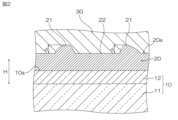
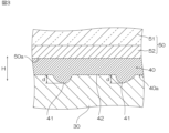
Y1,Y2 電極付き基材フィルム
10 基材フィルム
11 樹脂フィルム
20 電極層(第1電極層)
20a,40a 表面
21,41 隆起部
30 調光層
40 電極層(第2電極層)
Claims (4)
- 基材フィルムと、第1電極層と、調光層と、第2電極層とを厚さ方向にこの順で備える調光フィルムであって、
前記第1電極層における前記調光層の側の表面が、高さ3nm以上、8nm以下の隆起部を有し、
前記第1電極層の厚さが、30nm以上である、調光フィルム。 - 前記第2電極層における前記調光層の側の表面が、高さ3nm以上の隆起部を有する、請求項1に記載の調光フィルム。
- 前記基材フィルムが、近赤外線吸収層および/または近赤外線反射層を有する、請求項1に記載の調光フィルム。
- 波長800nm~1300nmでの平均透過率が50%以下である、請求項1から3のいずれか一つに記載の調光フィルム。
Priority Applications (8)
| Application Number | Priority Date | Filing Date | Title |
|---|---|---|---|
| JP2023017382A JP7581396B2 (ja) | 2023-02-08 | 2023-02-08 | 調光フィルム |
| CN202480010735.4A CN120641817A (zh) | 2023-02-08 | 2024-01-24 | 调光膜 |
| KR1020240010927A KR20240124201A (ko) | 2023-02-08 | 2024-01-24 | 조광 필름 |
| PCT/JP2024/002010 WO2024166684A1 (ja) | 2023-02-08 | 2024-01-24 | 調光フィルム |
| CN202480003469.2A CN119585672A (zh) | 2023-02-08 | 2024-01-24 | 调光膜 |
| PCT/JP2024/002009 WO2024166683A1 (ja) | 2023-02-08 | 2024-01-24 | 調光フィルム |
| KR1020247031958A KR102792308B1 (ko) | 2023-02-08 | 2024-01-24 | 조광 필름 |
| CN202410176700.XA CN118466075A (zh) | 2023-02-08 | 2024-02-08 | 调光薄膜 |
Applications Claiming Priority (1)
| Application Number | Priority Date | Filing Date | Title |
|---|---|---|---|
| JP2023017382A JP7581396B2 (ja) | 2023-02-08 | 2023-02-08 | 調光フィルム |
Publications (2)
| Publication Number | Publication Date |
|---|---|
| JP2024112408A JP2024112408A (ja) | 2024-08-21 |
| JP7581396B2 true JP7581396B2 (ja) | 2024-11-12 |
Family
ID=92156732
Family Applications (1)
| Application Number | Title | Priority Date | Filing Date |
|---|---|---|---|
| JP2023017382A Active JP7581396B2 (ja) | 2023-02-08 | 2023-02-08 | 調光フィルム |
Country Status (3)
| Country | Link |
|---|---|
| JP (1) | JP7581396B2 (ja) |
| KR (1) | KR20240124201A (ja) |
| CN (1) | CN118466075A (ja) |
Citations (5)
| Publication number | Priority date | Publication date | Assignee | Title |
|---|---|---|---|---|
| JP2019003060A (ja) | 2017-06-15 | 2019-01-10 | 国立大学法人千葉大学 | エレクトロクロミック表示素子 |
| JP2020134575A (ja) | 2019-02-14 | 2020-08-31 | 凸版印刷株式会社 | 調光体 |
| JP2021173825A (ja) | 2020-04-22 | 2021-11-01 | 日本放送協会 | 透過率可変素子及びその製造方法 |
| WO2022030582A1 (ja) | 2020-08-07 | 2022-02-10 | Agc株式会社 | 合わせガラス |
| JP2024034702A (ja) | 2022-09-01 | 2024-03-13 | Toppanホールディングス株式会社 | 調光シート |
Family Cites Families (1)
| Publication number | Priority date | Publication date | Assignee | Title |
|---|---|---|---|---|
| JP7171181B2 (ja) | 2017-12-01 | 2022-11-15 | 日東電工株式会社 | 調光フィルム |
-
2023
- 2023-02-08 JP JP2023017382A patent/JP7581396B2/ja active Active
-
2024
- 2024-01-24 KR KR1020240010927A patent/KR20240124201A/ko active Pending
- 2024-02-08 CN CN202410176700.XA patent/CN118466075A/zh active Pending
Patent Citations (5)
| Publication number | Priority date | Publication date | Assignee | Title |
|---|---|---|---|---|
| JP2019003060A (ja) | 2017-06-15 | 2019-01-10 | 国立大学法人千葉大学 | エレクトロクロミック表示素子 |
| JP2020134575A (ja) | 2019-02-14 | 2020-08-31 | 凸版印刷株式会社 | 調光体 |
| JP2021173825A (ja) | 2020-04-22 | 2021-11-01 | 日本放送協会 | 透過率可変素子及びその製造方法 |
| WO2022030582A1 (ja) | 2020-08-07 | 2022-02-10 | Agc株式会社 | 合わせガラス |
| JP2024034702A (ja) | 2022-09-01 | 2024-03-13 | Toppanホールディングス株式会社 | 調光シート |
Also Published As
| Publication number | Publication date |
|---|---|
| KR20240124201A (ko) | 2024-08-16 |
| CN118466075A (zh) | 2024-08-09 |
| JP2024112408A (ja) | 2024-08-21 |
Similar Documents
| Publication | Publication Date | Title |
|---|---|---|
| JP7278372B2 (ja) | 透明導電性フィルム | |
| WO2020031632A1 (ja) | 光透過性導電フィルムおよび調光フィルム | |
| JP7581396B2 (ja) | 調光フィルム | |
| JP7561957B1 (ja) | 調光フィルム | |
| JP7549117B1 (ja) | 調光フィルム | |
| WO2024166684A1 (ja) | 調光フィルム | |
| KR102792308B1 (ko) | 조광 필름 | |
| JP7068558B2 (ja) | 透明導電性フィルム | |
| JP7418506B1 (ja) | 透明導電性フィルム | |
| KR102695635B1 (ko) | 투명 도전성 필름 | |
| JP7784421B2 (ja) | フィルムヒータ、及び、ヒータ付きガラス | |
| KR102698069B1 (ko) | 투명 도전성 필름 | |
| CN111554431A (zh) | 导电性薄膜和触摸面板 | |
| JP7509852B2 (ja) | 透明導電性フィルム | |
| JPH02199428A (ja) | 調光積層体 | |
| JP3931806B2 (ja) | プラズマディスプレイ用電磁波シールドフィルムの製法およびプラズマディスプレイパネル用前面フィルター | |
| JP6954444B2 (ja) | 透明導電体、調光体及び電子デバイス | |
| JP5895089B1 (ja) | 熱線遮蔽積層体および該積層体を用いた窓ガラス | |
| WO2025041569A1 (ja) | 近赤外線遮蔽膜付きガラスフィルムと近赤外線遮蔽膜積層体、および、近赤外線遮蔽膜付きガラスフィルムの製造方法と近赤外線遮蔽膜積層体の製造方法 | |
| WO2016199661A1 (ja) | 熱線遮蔽積層体および該積層体を用いた窓ガラス |
Legal Events
| Date | Code | Title | Description |
|---|---|---|---|
| A521 | Request for written amendment filed |
Free format text: JAPANESE INTERMEDIATE CODE: A523 Effective date: 20240507 |
|
| A621 | Written request for application examination |
Free format text: JAPANESE INTERMEDIATE CODE: A621 Effective date: 20240507 |
|
| A871 | Explanation of circumstances concerning accelerated examination |
Free format text: JAPANESE INTERMEDIATE CODE: A871 Effective date: 20240507 |
|
| A131 | Notification of reasons for refusal |
Free format text: JAPANESE INTERMEDIATE CODE: A131 Effective date: 20240528 |
|
| A521 | Request for written amendment filed |
Free format text: JAPANESE INTERMEDIATE CODE: A523 Effective date: 20240626 |
|
| A131 | Notification of reasons for refusal |
Free format text: JAPANESE INTERMEDIATE CODE: A131 Effective date: 20240730 |
|
| A521 | Request for written amendment filed |
Free format text: JAPANESE INTERMEDIATE CODE: A523 Effective date: 20240912 |
|
| TRDD | Decision of grant or rejection written | ||
| A01 | Written decision to grant a patent or to grant a registration (utility model) |
Free format text: JAPANESE INTERMEDIATE CODE: A01 Effective date: 20241022 |
|
| A61 | First payment of annual fees (during grant procedure) |
Free format text: JAPANESE INTERMEDIATE CODE: A61 Effective date: 20241030 |
|
| R150 | Certificate of patent or registration of utility model |
Ref document number: 7581396 Country of ref document: JP Free format text: JAPANESE INTERMEDIATE CODE: R150 |