JP7581396B2 - Light control film - Google Patents
Light control film Download PDFInfo
- Publication number
- JP7581396B2 JP7581396B2 JP2023017382A JP2023017382A JP7581396B2 JP 7581396 B2 JP7581396 B2 JP 7581396B2 JP 2023017382 A JP2023017382 A JP 2023017382A JP 2023017382 A JP2023017382 A JP 2023017382A JP 7581396 B2 JP7581396 B2 JP 7581396B2
- Authority
- JP
- Japan
- Prior art keywords
- film
- layer
- electrode layer
- light
- resin
- Prior art date
- Legal status (The legal status is an assumption and is not a legal conclusion. Google has not performed a legal analysis and makes no representation as to the accuracy of the status listed.)
- Active
Links
Images


Classifications
-
- G—PHYSICS
- G02—OPTICS
- G02F—OPTICAL DEVICES OR ARRANGEMENTS FOR THE CONTROL OF LIGHT BY MODIFICATION OF THE OPTICAL PROPERTIES OF THE MEDIA OF THE ELEMENTS INVOLVED THEREIN; NON-LINEAR OPTICS; FREQUENCY-CHANGING OF LIGHT; OPTICAL LOGIC ELEMENTS; OPTICAL ANALOGUE/DIGITAL CONVERTERS
- G02F1/00—Devices or arrangements for the control of the intensity, colour, phase, polarisation or direction of light arriving from an independent light source, e.g. switching, gating or modulating; Non-linear optics
- G02F1/01—Devices or arrangements for the control of the intensity, colour, phase, polarisation or direction of light arriving from an independent light source, e.g. switching, gating or modulating; Non-linear optics for the control of the intensity, phase, polarisation or colour
- G02F1/13—Devices or arrangements for the control of the intensity, colour, phase, polarisation or direction of light arriving from an independent light source, e.g. switching, gating or modulating; Non-linear optics for the control of the intensity, phase, polarisation or colour based on liquid crystals, e.g. single liquid crystal display cells
- G02F1/133—Constructional arrangements; Operation of liquid crystal cells; Circuit arrangements
- G02F1/1333—Constructional arrangements; Manufacturing methods
- G02F1/1343—Electrodes
-
- G—PHYSICS
- G02—OPTICS
- G02F—OPTICAL DEVICES OR ARRANGEMENTS FOR THE CONTROL OF LIGHT BY MODIFICATION OF THE OPTICAL PROPERTIES OF THE MEDIA OF THE ELEMENTS INVOLVED THEREIN; NON-LINEAR OPTICS; FREQUENCY-CHANGING OF LIGHT; OPTICAL LOGIC ELEMENTS; OPTICAL ANALOGUE/DIGITAL CONVERTERS
- G02F1/00—Devices or arrangements for the control of the intensity, colour, phase, polarisation or direction of light arriving from an independent light source, e.g. switching, gating or modulating; Non-linear optics
- G02F1/01—Devices or arrangements for the control of the intensity, colour, phase, polarisation or direction of light arriving from an independent light source, e.g. switching, gating or modulating; Non-linear optics for the control of the intensity, phase, polarisation or colour
- G02F1/15—Devices or arrangements for the control of the intensity, colour, phase, polarisation or direction of light arriving from an independent light source, e.g. switching, gating or modulating; Non-linear optics for the control of the intensity, phase, polarisation or colour based on an electrochromic effect
- G02F1/153—Constructional details
-
- G—PHYSICS
- G02—OPTICS
- G02F—OPTICAL DEVICES OR ARRANGEMENTS FOR THE CONTROL OF LIGHT BY MODIFICATION OF THE OPTICAL PROPERTIES OF THE MEDIA OF THE ELEMENTS INVOLVED THEREIN; NON-LINEAR OPTICS; FREQUENCY-CHANGING OF LIGHT; OPTICAL LOGIC ELEMENTS; OPTICAL ANALOGUE/DIGITAL CONVERTERS
- G02F1/00—Devices or arrangements for the control of the intensity, colour, phase, polarisation or direction of light arriving from an independent light source, e.g. switching, gating or modulating; Non-linear optics
- G02F1/01—Devices or arrangements for the control of the intensity, colour, phase, polarisation or direction of light arriving from an independent light source, e.g. switching, gating or modulating; Non-linear optics for the control of the intensity, phase, polarisation or colour
- G02F1/13—Devices or arrangements for the control of the intensity, colour, phase, polarisation or direction of light arriving from an independent light source, e.g. switching, gating or modulating; Non-linear optics for the control of the intensity, phase, polarisation or colour based on liquid crystals, e.g. single liquid crystal display cells
- G02F1/133—Constructional arrangements; Operation of liquid crystal cells; Circuit arrangements
- G02F1/1333—Constructional arrangements; Manufacturing methods
- G02F1/1334—Constructional arrangements; Manufacturing methods based on polymer dispersed liquid crystals, e.g. microencapsulated liquid crystals
-
- G—PHYSICS
- G02—OPTICS
- G02F—OPTICAL DEVICES OR ARRANGEMENTS FOR THE CONTROL OF LIGHT BY MODIFICATION OF THE OPTICAL PROPERTIES OF THE MEDIA OF THE ELEMENTS INVOLVED THEREIN; NON-LINEAR OPTICS; FREQUENCY-CHANGING OF LIGHT; OPTICAL LOGIC ELEMENTS; OPTICAL ANALOGUE/DIGITAL CONVERTERS
- G02F1/00—Devices or arrangements for the control of the intensity, colour, phase, polarisation or direction of light arriving from an independent light source, e.g. switching, gating or modulating; Non-linear optics
- G02F1/01—Devices or arrangements for the control of the intensity, colour, phase, polarisation or direction of light arriving from an independent light source, e.g. switching, gating or modulating; Non-linear optics for the control of the intensity, phase, polarisation or colour
- G02F1/15—Devices or arrangements for the control of the intensity, colour, phase, polarisation or direction of light arriving from an independent light source, e.g. switching, gating or modulating; Non-linear optics for the control of the intensity, phase, polarisation or colour based on an electrochromic effect
- G02F1/153—Constructional details
- G02F1/155—Electrodes
-
- G—PHYSICS
- G02—OPTICS
- G02F—OPTICAL DEVICES OR ARRANGEMENTS FOR THE CONTROL OF LIGHT BY MODIFICATION OF THE OPTICAL PROPERTIES OF THE MEDIA OF THE ELEMENTS INVOLVED THEREIN; NON-LINEAR OPTICS; FREQUENCY-CHANGING OF LIGHT; OPTICAL LOGIC ELEMENTS; OPTICAL ANALOGUE/DIGITAL CONVERTERS
- G02F1/00—Devices or arrangements for the control of the intensity, colour, phase, polarisation or direction of light arriving from an independent light source, e.g. switching, gating or modulating; Non-linear optics
- G02F1/01—Devices or arrangements for the control of the intensity, colour, phase, polarisation or direction of light arriving from an independent light source, e.g. switching, gating or modulating; Non-linear optics for the control of the intensity, phase, polarisation or colour
- G02F1/15—Devices or arrangements for the control of the intensity, colour, phase, polarisation or direction of light arriving from an independent light source, e.g. switching, gating or modulating; Non-linear optics for the control of the intensity, phase, polarisation or colour based on an electrochromic effect
- G02F1/153—Constructional details
- G02F1/157—Structural association of cells with optical devices, e.g. reflectors or illuminating devices
-
- G—PHYSICS
- G02—OPTICS
- G02F—OPTICAL DEVICES OR ARRANGEMENTS FOR THE CONTROL OF LIGHT BY MODIFICATION OF THE OPTICAL PROPERTIES OF THE MEDIA OF THE ELEMENTS INVOLVED THEREIN; NON-LINEAR OPTICS; FREQUENCY-CHANGING OF LIGHT; OPTICAL LOGIC ELEMENTS; OPTICAL ANALOGUE/DIGITAL CONVERTERS
- G02F1/00—Devices or arrangements for the control of the intensity, colour, phase, polarisation or direction of light arriving from an independent light source, e.g. switching, gating or modulating; Non-linear optics
- G02F1/01—Devices or arrangements for the control of the intensity, colour, phase, polarisation or direction of light arriving from an independent light source, e.g. switching, gating or modulating; Non-linear optics for the control of the intensity, phase, polarisation or colour
- G02F1/165—Devices or arrangements for the control of the intensity, colour, phase, polarisation or direction of light arriving from an independent light source, e.g. switching, gating or modulating; Non-linear optics for the control of the intensity, phase, polarisation or colour based on translational movement of particles in a fluid under the influence of an applied field
- G02F1/1675—Constructional details
- G02F1/1676—Electrodes
-
- G—PHYSICS
- G02—OPTICS
- G02F—OPTICAL DEVICES OR ARRANGEMENTS FOR THE CONTROL OF LIGHT BY MODIFICATION OF THE OPTICAL PROPERTIES OF THE MEDIA OF THE ELEMENTS INVOLVED THEREIN; NON-LINEAR OPTICS; FREQUENCY-CHANGING OF LIGHT; OPTICAL LOGIC ELEMENTS; OPTICAL ANALOGUE/DIGITAL CONVERTERS
- G02F2201/00—Constructional arrangements not provided for in groups G02F1/00 - G02F7/00
- G02F2201/08—Constructional arrangements not provided for in groups G02F1/00 - G02F7/00 light absorbing layer
- G02F2201/083—Constructional arrangements not provided for in groups G02F1/00 - G02F7/00 light absorbing layer infrared absorbing
Landscapes
- Physics & Mathematics (AREA)
- Nonlinear Science (AREA)
- General Physics & Mathematics (AREA)
- Optics & Photonics (AREA)
- Chemical & Material Sciences (AREA)
- Mathematical Physics (AREA)
- Crystallography & Structural Chemistry (AREA)
- Dispersion Chemistry (AREA)
- Liquid Crystal (AREA)
- Laminated Bodies (AREA)
- Electrochromic Elements, Electrophoresis, Or Variable Reflection Or Absorption Elements (AREA)
- Electroluminescent Light Sources (AREA)
Description
本発明は、調光フィルムに関する。 The present invention relates to a light control film.
建物および乗り物等の窓ガラスに貼り合わされる調光フィルムが知られている。調光フィルムは、調光部と、当該調光部を支持する透明な基材フィルムとを備える。調光部は、例えば、透明導電層と、調光層と、透明導電層とを、厚さ方向にこの順で備える。調光層は、二つの透明導電層によって挟まれる。調光層は、エレクトクロミック(EC)材料から形成される。EC材料は、例えば、電気化学的酸化還元により、有色の非透明状態と透明状態との間で可逆的に変化可能な材料である。各透明導電層は、電極である。透明導電層間の電圧のオン・オフにより、調光層が、例えば、非透明状態(遮光状態)と透明状態(非遮光状態)との間で切り替えられる。このような調光フィルムが貼り合わされた窓ガラスでは、透明導電層間の電圧のオン・オフにより、当該調光フィルム付き窓ガラスに対する可視光などの光の透過率が、切り替えられる(光透過率のスイッチング制御)。このような調光フィルムに関する技術については、例えば下記の特許文献1に記載されている。
A light control film that is attached to the window glass of a building, vehicle, etc. is known. The light control film includes a light control section and a transparent substrate film that supports the light control section. The light control section includes, for example, a transparent conductive layer, a light control layer, and a transparent conductive layer in this order in the thickness direction. The light control layer is sandwiched between two transparent conductive layers. The light control layer is formed from an electrochromic (EC) material. The EC material is a material that can be reversibly changed between a colored non-transparent state and a transparent state, for example, by electrochemical oxidation-reduction. Each transparent conductive layer is an electrode. By turning on and off the voltage between the transparent conductive layers, the light control layer is switched, for example, between a non-transparent state (light blocking state) and a transparent state (non-light blocking state). In a window glass to which such a light control film is attached, the transmittance of light such as visible light through the window glass with the light control film can be switched by turning on and off the voltage between the transparent conductive layers (switching control of light transmittance). The technology related to this type of light control film is described, for example, in
建物内および乗り物内の快適性向上および冷房負荷の低減等の観点から、調光フィルムには、太陽光に対する遮熱性を有することが求められる。 To improve comfort inside buildings and vehicles and reduce the cooling load, light-control films are required to have heat-blocking properties against sunlight.
一方、本発明者らは、調光フィルムに関し、次のような知見を得た。電極層(透明導電層)は、太陽光中の熱線(放射によって熱を伝える近赤外線等の電磁波)に対して有意な反射性を有する自由電子を、キャリアとして含有する。調光フィルムでは、そのような電極層が、調光層に対して全面的に設けられている。すなわち、調光フィルムにおける平面視での電極層の占有面積割合は、大きい。このような調光フィルムでは、電極層におけるキャリア数の調整により、太陽光に対する同フィルムの遮熱性を効率よく制御できる。本発明は、このような知見に基づく。 On the other hand, the inventors have discovered the following about light-control films. The electrode layer (transparent conductive layer) contains free electrons as carriers that have significant reflectivity to heat rays in sunlight (electromagnetic waves such as near-infrared rays that transmit heat by radiation). In light-control films, such an electrode layer is provided over the entire surface of the light-control layer. In other words, the electrode layer occupies a large area in a planar view of the light-control film. In such light-control films, the heat-shielding properties of the film against sunlight can be efficiently controlled by adjusting the number of carriers in the electrode layer. The present invention is based on such findings.
本発明は、太陽光に対する良好な遮熱性を実現するのに適した調光フィルムを提供する。 The present invention provides a light-control film that is suitable for achieving good heat shielding properties against sunlight.
本発明[1]は、基材フィルムと、第1電極層と、調光層と、第2電極層とを厚さ方向にこの順で備える調光フィルムであって、前記第1電極層における前記調光層の側の表面が、高さ3nm以上の隆起部を有する、調光フィルムを含む。 The present invention [1] includes a light-control film that includes a base film, a first electrode layer, a light-control layer, and a second electrode layer in this order in the thickness direction, and in which the surface of the first electrode layer facing the light-control layer has a raised portion having a height of 3 nm or more.
本発明[2]は、前記第2電極層における前記調光層の側の表面が、高さ3nm以上の隆起部を有する、上記[1]に記載の調光フィルムを含む。 The present invention [2] includes the light-control film described in [1] above, in which the surface of the second electrode layer facing the light-control layer has a protrusion having a height of 3 nm or more.
本発明[3]は、前記基材フィルムが、近赤外線吸収層および/または近赤外線反射層を有する、上記[1]または[2]に記載の調光フィルムを含む。 The present invention [3] includes the light control film described in [1] or [2] above, in which the base film has a near-infrared absorbing layer and/or a near-infrared reflective layer.
本発明[4]は、波長800nm~1300nmでの平均透過率が50%以下である、上記[1]から[3]のいずれか一つに記載の調光フィルムを含む。 The present invention [4] includes the light control film according to any one of [1] to [3] above, which has an average transmittance of 50% or less at wavelengths of 800 nm to 1,300 nm.
本発明の調光フィルムは、上記のように、基材フィルムと、第1電極層と、調光層と、第2電極層とを厚さ方向にこの順で備え、第1電極層における調光層側の表面が、高さ3nm以上の隆起部を有する。第1電極層が、3nm以上の有意な高さの隆起部を有することは、第1電極層全体の平均厚さを確保するのに適する(第1電極層がそのような隆起部を有する場合、隆起部を有しない場合よりも、同層全体の平均厚さは大きい)。このような調光フィルムは、第1電極層における平面視の単位面積あたりの自由電子数(キャリア数)を確保するのに適する。第1電極層における単位面積あたりの自由電子数が多いほど、当該第1電極層の、太陽光中の熱線に対する反射性は高い。熱線に対する第1電極層の反射性が高いほど、そのような第1電極層を備える調光フィルムの、熱線に対する遮蔽性(遮熱性)は高い。したがって、本発明の調光フィルムは、太陽光に対する良好な遮熱性を実現するのに適する。 As described above, the light-controlling film of the present invention comprises a base film, a first electrode layer, a light-controlling layer, and a second electrode layer in this order in the thickness direction, and the surface of the first electrode layer on the side of the light-controlling layer has a raised portion having a height of 3 nm or more. The first electrode layer having a raised portion with a significant height of 3 nm or more is suitable for ensuring the average thickness of the entire first electrode layer (when the first electrode layer has such a raised portion, the average thickness of the entire layer is larger than when the first electrode layer does not have the raised portion). Such a light-controlling film is suitable for ensuring the number of free electrons (number of carriers) per unit area in a planar view in the first electrode layer. The greater the number of free electrons per unit area in the first electrode layer, the higher the reflectivity of the first electrode layer against heat rays in sunlight. The higher the reflectivity of the first electrode layer against heat rays, the higher the shielding property (heat shielding property) of the light-controlling film comprising such a first electrode layer against heat rays. Therefore, the light-controlling film of the present invention is suitable for achieving good heat shielding property against sunlight.
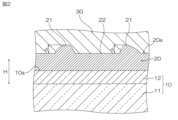
本発明の一実施形態としての調光フィルムXは、基材フィルム10(第1基材フィルム)と、電極層20(第1電極層)と、調光層30と、電極層40(第2電極層)と、基材フィルム50(第2基材フィルム)とを、厚さ方向Hにこの順で備える。基材フィルム10は、第1面10aと、当該第1面10aとは反対側の第2面10bとを有する。電極層20は、第1面10a上に配置されている。電極層20と第1面10aとは、互いに接する。また、電極層20は、調光層30側(基材フィルム10とは反対側)に表面20aを有する。調光層30は、表面20a上に配置されている。調光層30と表面20aとは、互いに接する。電極層40は、調光層30上に配置されている。電極層40は、調光層30側(基材フィルム50とは反対側)に表面40aを有する。表面40aと調光層30とは、互いに接する。基材フィルム50は、電極層40上に配置されている。基材フィルム50は、電極層40側の第1面50aと、当該第1面50aとは反対側の第2面50bとを有する。電極層40と第1面50aとは、互いに接する。また、調光フィルムXは、厚さ方向Hと直交する方向(面方向)に広がるシート形状を有する。このような調光フィルムXは、例えば、建物および乗り物等の窓ガラスに組付けられる調光フィルムである。
The light control film X as one embodiment of the present invention includes a base film 10 (first base film), an electrode layer 20 (first electrode layer), a
調光フィルムXにおいて、基材フィルム10と電極層20とは、電極付き基材フィルムY1を形成する。
In the light control film X, the
基材フィルム10は、本実施形態では、樹脂フィルム11と、硬化樹脂層12とを、厚さ方向Hに順に備える。硬化樹脂層12は、樹脂フィルム11に接する。硬化樹脂層12は、基材フィルム10の第1面10aを形成する。
In this embodiment, the
樹脂フィルム11は、調光フィルムXの強度を確保する基材である。また、樹脂フィルム11は、可撓性を有する透明な樹脂フィルムである。樹脂フィルム11の材料としては、例えば、ポリエステル樹脂、ポリオレフィン樹脂、アクリル樹脂、ポリカーボネート樹脂、ポリエーテルスルフォン樹脂、ポリアリレート樹脂、メラミン樹脂、ポリアミド樹脂、ポリイミド樹脂、セルロース樹脂、およびポリスチレン樹脂が挙げられる。ポリエステル樹脂としては、例えば、ポリエチレンテレフタレート(PET)、ポリブチレンテレフタレート、およびポリエチレンナフタレートが挙げられる。ポリオレフィン樹脂としては、例えば、ポリエチレン、ポリプロピレン、およびシクロオレフィンポリマーが挙げられる。アクリル樹脂としては、例えばポリメタクリレートが挙げられる。樹脂フィルム11の材料としては、例えば透明性および強度の観点から、好ましくはポリエステル樹脂が用いられ、より好ましくはPETが用いられる。
The
樹脂フィルム11における硬化樹脂層12側の表面は、表面改質処理されていてもよい。表面改質処理としては、例えば、コロナ処理、プラズマ処理、オゾン処理、プライマー処理、グロー処理、およびカップリング剤処理が挙げられる(後記の樹脂フィルム51に関する表面改質処理についても同様である)。
The surface of the
樹脂フィルム11の厚さは、調光フィルムXの強度を確保する観点から、好ましくは10μm以上、より好ましくは20μm以上、更に好ましくは30μm以上である。樹脂フィルム11の厚さは、ロールトゥロール方式における樹脂フィルム11の取り扱い性を確保する観点から、好ましくは300μm以下、より好ましくは200μm以下、更に好ましくは150μm以下である。
The thickness of the
樹脂フィルム11の可視光透過率は、調光フィルムの透明状態時に求められる透明性を調光フィルムXにおいて確保する観点から、好ましくは70%以上、より好ましくは80%以上、更に好ましくは85%以上である。樹脂フィルム11の可視光透過率は、例えば100%以下である。可視光透過率とは、波長380nm~780nmの範囲での透過率とする。
The visible light transmittance of the
硬化樹脂層12は、本実施形態では、調光フィルムXの光学特性を良化するための光学調整層(屈折率調整層)である。硬化樹脂層12は、後述の透明導電層形成工程(図4B)において、樹脂フィルム11から発生する水分や有機ガスを遮断する機能を有してもよい。硬化樹脂層12は、本実施形態では、第1硬化型樹脂組成物の硬化物である。第1硬化型樹脂組成物は、樹脂を含有する。当該樹脂としては、例えば、メラミン樹脂、アルキド樹脂、有機シラン縮合物、ポリエステル樹脂、アクリルウレタン樹脂、アクリル樹脂(アクリルウレタン樹脂を除く)、ウレタン樹脂(アクリルウレタン樹脂を除く)、アミド樹脂、シリコーン樹脂、およびエポキシ樹脂が挙げられる。これら樹脂は、単独で用いられてもよいし、二種類以上が併用されてもよい。基材フィルム10に対する電極層20の密着性を確保する観点から、樹脂としては、好ましくは、メラミン樹脂、アルキド樹脂および有機シラン縮合物からなる群より選択される少なくとも一つが用いられる。また、第1硬化型樹脂組成物は、紫外線硬化型の樹脂組成物であってもよいし、熱硬化型の樹脂組成物であってもよい。
In this embodiment, the cured
硬化樹脂層12の、樹脂フィルム11とは反対側の表面(第1面10a)は、硬化樹脂層12上に形成される電極層20の平均厚さを確保する観点から、好ましくは、高さ3nm以上の隆起部を有せず、より好ましくは、高さ2nm以上の隆起部を有せず、更に好ましくは、高さ1nm以上の隆起部を有しない。隆起部を有しない硬化樹脂層12を形成する観点から、第1硬化型樹脂組成物は、粒子を含有しないのが好ましい。
From the viewpoint of ensuring the average thickness of the
硬化樹脂層12の厚さは、調光フィルムXの透過特性を良化する観点から、好ましくは5nm以上、より好ましくは10nm以上、更に好ましくは20nm以上、特に好ましくは30nm以上である。硬化樹脂層12の厚さは、調光フィルムXの薄型化の観点から、好ましくは1000nm以下、より好ましくは50nm以下、更に好ましくは40nm以下である。
From the viewpoint of improving the transmission characteristics of the light-controlling film X, the thickness of the cured
基材フィルム10は、樹脂フィルム11に対して硬化樹脂層12とは反対側に他の硬化樹脂層を有してもよい。他の硬化樹脂層としては、例えば、ハードコート層およびアンチブロッキング層が挙げられる。
The
他の硬化樹脂層は、例えば、第2硬化型樹脂組成物の硬化物である。第2硬化型樹脂組成物は、樹脂を含有する。当該樹脂としては、例えば、ポリエステル樹脂、アクリルウレタン樹脂、アクリル樹脂(アクリルウレタン樹脂を除く)、ウレタン樹脂(アクリルウレタン樹脂を除く)、アミド樹脂、シリコーン樹脂、エポキシ樹脂、およびメラミン樹脂が挙げられる。これら樹脂は、単独で用いられてもよいし、二種類以上が併用されてもよい。第2硬化型樹脂組成物は、紫外線硬化型の樹脂組成物であってもよいし、熱硬化型の樹脂組成物であってもよい。 The other cured resin layer is, for example, a cured product of a second curable resin composition. The second curable resin composition contains a resin. Examples of the resin include polyester resin, acrylic urethane resin, acrylic resin (excluding acrylic urethane resin), urethane resin (excluding acrylic urethane resin), amide resin, silicone resin, epoxy resin, and melamine resin. These resins may be used alone or in combination of two or more kinds. The second curable resin composition may be an ultraviolet-curable resin composition or a thermosetting resin composition.
第2硬化型樹脂組成物は、粒子を含有してもよい。当該粒子としては、例えば、無機酸化物粒子および有機粒子が挙げられる。無機酸化物粒子の材料としては、例えば、シリカ、アルミナ、チタニア、ジルコニア、酸化カルシウム、酸化スズ、酸化インジウム、酸化カドミウム、および酸化アンチモンが挙げられる。有機粒子の材料としては、例えば、ポリメチルメタクリレート、ポリスチレン、ポリウレタン、アクリル・スチレン共重合体、ベンゾグアナミン、メラミン、およびポリカーボネートが挙げられる。粒子としては、好ましくは無機酸化物粒子が用いられ、より好ましくは、シリカ粒子および/またはジルコニア粒子が用いられる。 The second curable resin composition may contain particles. Examples of the particles include inorganic oxide particles and organic particles. Examples of materials for inorganic oxide particles include silica, alumina, titania, zirconia, calcium oxide, tin oxide, indium oxide, cadmium oxide, and antimony oxide. Examples of materials for organic particles include polymethyl methacrylate, polystyrene, polyurethane, acrylic-styrene copolymer, benzoguanamine, melamine, and polycarbonate. As the particles, inorganic oxide particles are preferably used, and more preferably silica particles and/or zirconia particles are used.
他の硬化樹脂層の厚さは、当該硬化樹脂層の機能を確保する観点から、好ましくは0.5μm以上、より好ましくは1μm以上、更に好ましくは2μm以上である。硬化樹脂層12の厚さは、調光フィルムXの薄型化の観点から、好ましくは10μm以下、より好ましくは5μm以下、更に好ましくは3μm以下である。
The thickness of the other cured resin layers is preferably 0.5 μm or more, more preferably 1 μm or more, and even more preferably 2 μm or more, from the viewpoint of ensuring the functionality of the cured resin layers. The thickness of the cured
基材フィルム10の厚さは、調光フィルムXの取り扱い性を確保する観点から、好ましくは10μm以上、より好ましくは30μm以上、更に好ましくは50μm以上である。基材フィルム10の厚さは、調光フィルムXの薄型化の観点から、好ましくは500μm以下、より好ましくは300μm以下、更に好ましくは200μm以下、一層好ましくは150μm以下である。
From the viewpoint of ensuring the ease of handling of the light-control film X, the thickness of the
基材フィルム10の可視光透過率は、調光フィルムの透明状態時に求められる透明性を調光フィルムXにおいて確保する観点から、好ましくは70%以上、より好ましくは80%以上、更に好ましくは85%以上である。基材フィルム10の可視光透過率は、例えば100%以下である。
The visible light transmittance of the
基材フィルム10は、好ましくは、近赤外線吸収層および/または近赤外線反射層を有する。近赤外線吸収層とは、近赤外線(波長700nm~2500nm)に対して有意な吸収能を示す層とする。近赤外線反射層とは、近赤外線(波長700nm~2500nm)に対して有意な反射能を示す層とする。
The
近赤外線吸収層は、樹脂フィルム11と硬化樹脂層12との間に配置されてもよいし、樹脂フィルム11に対して硬化樹脂層12とは反対側に配置されてもよい。樹脂フィルム11が、近赤外線吸収層であってもよいし、近赤外線吸収層を含む多層構造を有してもよい。近赤外線吸収層は、例えば、近赤外線吸収剤と、バインダー樹脂とを含む。近赤外線吸収剤としては、例えば、無機近赤外線吸収剤および有機近赤外線吸収剤が挙げられる。無機近赤外線吸収剤としては、例えば、CFM複合酸化物粒子および酸化タングステン粒子が挙げられる。CFM複合酸化物とは、銅と鉄とマンガンとの複合酸化物である。バインダー樹脂の材料としては、例えば、樹脂フィルム11に関して上記した材料が挙げられる。
The near-infrared absorbing layer may be disposed between the
近赤外線反射層は、樹脂フィルム11と硬化樹脂層12との間に配置されてもよいし、樹脂フィルム11に対して硬化樹脂層12とは反対側に配置されてもよい。樹脂フィルム11が、近赤外線反射層であってもよいし、近赤外線反射層を含む多層構造を有してもよい。近赤外線反射層は、例えば、光学特性の異なる複数の樹脂薄層を含む多層構造を有し、好ましくは、光学特性の異なる第1樹脂薄層および第2樹脂薄層が厚さ方向Hに交互に配置された多層構造を有する。光学特性としては、例えば、面内平均屈折率が挙げられる。第1樹脂薄層と第2樹脂薄層との面内平均屈折率の差は、好ましくは0.01以上、より好ましくは0.03以上であり、また、好ましくは0.15以下、より好ましくは0.12以下である。多層構造を形成する樹脂薄層の積層数は、例えば20以上であり、また、例えば700以下である。樹脂薄層の材料としては、例えば、樹脂フィルム11に関して上記した材料が挙げられる。
The near-infrared reflective layer may be disposed between the
電極層20は、光透過性と導電性とを兼ね備える層である。このような電極層20は、透明導電材料から形成されている。すなわち、電極層20は透明導電層である。透明導電材料としては、例えば、透明な導電性酸化物が挙げられる。
The
導電性酸化物としては、例えば、インジウム含有導電性酸化物およびアンチモン含有導電性酸化物が挙げられる。インジウム含有導電性酸化物としては、例えば、インジウムスズ複合酸化物(ITO)、インジウム亜鉛複合酸化物(IZO)、インジウムガリウム複合酸化物(IGO)、およびインジウムガリウム亜鉛複合酸化物(IGZO)が挙げられる。アンチモン含有導電性酸化物としては、例えば、アンチモンスズ複合酸化物(ATO)が挙げられる。高い透明性と良好な電気伝導性とを実現する観点からは、導電性酸化物としては、好ましくはインジウム含有導電性酸化物が用いられ、より好ましくはITOが用いられる。このITOは、InおよびSn以外の金属または半金属を、InおよびSnのそれぞれの含有量より少ない量で含有してもよい。 Examples of conductive oxides include indium-containing conductive oxides and antimony-containing conductive oxides. Examples of indium-containing conductive oxides include indium tin composite oxide (ITO), indium zinc composite oxide (IZO), indium gallium composite oxide (IGO), and indium gallium zinc composite oxide (IGZO). Examples of antimony-containing conductive oxides include antimony tin composite oxide (ATO). From the viewpoint of achieving high transparency and good electrical conductivity, indium-containing conductive oxides are preferably used as conductive oxides, and ITO is more preferably used. This ITO may contain metals or semimetals other than In and Sn in amounts less than the respective contents of In and Sn.
ITOにおける酸化インジウム(In2O3)および酸化スズ(SnO2)の合計含有量に対する酸化スズの含有量の割合は、好ましくは4質量%以上、より好ましくは6質量%以上、更に好ましくは8質量%以上、特に好ましくは9質量%以上である。このような構成は、後述の結晶化工程(図4C)において、透明導電層の結晶粒を成長させて、隆起部21を形成するのに好ましい。また、ITOにおける酸化インジウムおよび酸化スズの合計含有量に対する酸化スズの含有量の割合は、電極層20の低抵抗化の観点から、好ましくは15質量%以下、より好ましくは13質量%以下、更に好ましくは12質量%以下である。
The ratio of the content of tin oxide to the total content of indium oxide (In 2 O 3 ) and tin oxide (SnO 2 ) in ITO is preferably 4 mass% or more, more preferably 6 mass% or more, even more preferably 8 mass% or more, and particularly preferably 9 mass% or more. Such a configuration is preferable for growing crystal grains of the transparent conductive layer to form the
ITOにおける酸化スズ割合は、例えば次のようにして同定できる。まず、X線光電子分光法(X-ray Photoelectron Spectroscopy)により、測定対象物としてのITOにおけるインジウム原子(In)とスズ原子(Sn)の存在比率を求める。ITO中のInおよびSnの各存在比率から、ITO中のInの原子数に対するSnの原子数の比率を求める。これにより、ITOにおける酸化スズ割合が得られる。また、ITOにおける酸化スズ割合は、スパッタ成膜時に用いるITOターゲットの酸化スズ(SnO2)含有割合からも特定できる。 The tin oxide ratio in ITO can be identified, for example, as follows. First, the abundance ratio of indium atoms (In) and tin atoms (Sn) in ITO as a measurement target is obtained by X-ray photoelectron spectroscopy. From the abundance ratios of In and Sn in ITO, the ratio of the number of Sn atoms to the number of In atoms in ITO is obtained. This gives the tin oxide ratio in ITO. The tin oxide ratio in ITO can also be determined from the tin oxide (SnO 2 ) content of the ITO target used during sputtering film formation.
電極層20は、好ましくは結晶膜である。電極層20が結晶膜であることは、電極層20の低抵抗化の観点から好ましく、また、電極層20および調光フィルムXにおいて良好な赤外線反射特性を実現するのに好ましい。
The
導電性酸化物から形成された電極層(調光フィルムXでは電極層20,40)が結晶膜であることは、例えば、次の方法によって判断できる。まず、電極層を、濃度5質量%の塩酸に、20℃で15分間、浸漬する。次に、電極層を、水洗した後、乾燥する。次に、電極層の露出平面において、離隔距離15mmの一対の端子の間の抵抗(端子間抵抗)を測定する。この測定において、端子間抵抗が10kΩ以下である場合に、当該電極層が結晶膜であると判断できる。 Whether an electrode layer formed from a conductive oxide (electrode layers 20 and 40 in light control film X) is a crystalline film can be determined, for example, by the following method. First, the electrode layer is immersed in hydrochloric acid with a concentration of 5% by mass at 20°C for 15 minutes. Next, the electrode layer is washed with water and then dried. Next, the resistance between a pair of terminals separated by a distance of 15 mm (inter-terminal resistance) is measured on the exposed surface of the electrode layer. In this measurement, if the inter-terminal resistance is 10 kΩ or less, the electrode layer can be determined to be a crystalline film.
電極層20の表面20aは、図2に示すように、高さdが3nm以上の隆起部21を有する。隆起部21の高さdとは、厚さ方向Hにおける、表面20aの平坦面22から隆起部21の頂部までの距離である。電極層20が、3nm以上の有意な高さの隆起部21を有することは、電極層20全体の平均厚さを確保するのに適する(電極層20がそのような隆起部21を有する場合、隆起部21を有しない場合よりも、同層全体の平均厚さは大きい)。このことは、電極層20の平面視における単位面積あたりの自由電子数(キャリア数)を確保するのに適する。電極層20における当該自由電子数が多いほど、太陽光中の熱線(主に近赤外線)に対する電極層20の反射性は高く、従って、熱線に対する調光フィルムXの遮蔽性(遮熱性)は高い。調光フィルムXにおいて良好な遮熱性を確保する観点から、隆起部21の高さdは、好ましくは4nm以上、更に好ましくは5nm以上である。隆起部21の高さdは、電極層20の抵抗値の上昇を抑制する観点から、好ましくは20nm以下、より好ましくは10nm以下、更に好ましくは8nm以下である。隆起部の高さの測定方法は、実施例に関して後述するとおりである。
As shown in FIG. 2, the
電極層20の厚さは、隆起部21を形成する観点から、好ましくは30nm以上、より好ましくは50nm以上、更に好ましくは70nm以上、一層好ましくは90nm以上、特に好ましくは100nm以上である。電極層20の厚さとは、厚さ方向Hにおける、電極層20の基材フィルム10側表面から平坦面22までの距離とする。電極層20が厚い方ほど、後述の結晶化工程において透明導電層の結晶粒が大きく成長しやすく、従って、電極層20の表面20aにおいて隆起部21を形成しやすい。また、電極層20が厚いことは、電極層20の低抵抗化の観点からも好ましい。電極層20の厚さは、調光フィルムXの耐屈曲性(屈曲時の電極層20の割れの抑制等)を確保する観点から、好ましくは300nm以下、より好ましくは200nm以下、更に好ましくは150nm以下、一層好ましくは120nm以下である。
The thickness of the
電極層20の平面視における自由電子数(キャリア数)は、電極層20での遮熱性確保の観点から、好ましくは5×10¹⁵/cm2以上、より好ましくは8×1015/cm2以上、更に好ましくは10×1015/cm2以上、一層好ましくは11×1015/cm2以上である。電極層20の平面視における自由電子数(キャリア数)は、電極層20の可視光透過率を確保する観点から、好ましくは100×1015/cm2以下、より好ましくは60×1015/cm2以下、更に好ましくは40×1015/cm2以下である。電極層のキャリア数の測定方法は、実施例に関して後述するとおりである。
The number of free electrons (number of carriers) in the
電極層20の可視光透過率は、調光フィルムの透明状態時に求められる透明性を調光フィルムXにおいて確保する観点から、例えば50%以上であり、好ましくは70%以上、より好ましくは80%以上、更に好ましくは85%以上である。また、電極層20の可視光透過率は、例えば100%以下である。
The visible light transmittance of the
調光層30は、例えば、電流または電界の作用によって有色の非透明状態(遮光状態)と透明状態(非遮光状態)との間で可逆的に変化可能な材料である。調光層30としては、例えば、エレクトクロミック(EC)調光層、高分子分散型液晶(PDLC:polymer dispersed liquid crystal)を含む調光層、高分子ネットワーク型液晶(PNLC:polymer network liquid crystal)を含む調光層、および、SPD(suspended particle device)調光層が挙げられる。
The light-adjusting
EC調光層は、EC材料から形成される。EC材料は、電気化学的酸化還元により、有色の非透明状態(遮光状態)と透明状態(非遮光状態)との間で可逆的に変化可能な材料である。EC材料としては、無機EC材料および有機EC材料が挙げられる。無機EC材料としては、例えば、酸化タングステン、酸化バナジウム、酸化モリブデン、酸化イリジウム、酸化ロジウム、および窒化インジウムが挙げられる。有機EC材料としては、例えば、ポリアニリン、ビオロゲン、およびポリオキソタングステートが挙げられる。 The EC light control layer is formed from an EC material. The EC material is a material that can be reversibly changed between a colored non-transparent state (light-shielding state) and a transparent state (light-non-shielding state) by electrochemical oxidation and reduction. EC materials include inorganic EC materials and organic EC materials. Inorganic EC materials include, for example, tungsten oxide, vanadium oxide, molybdenum oxide, iridium oxide, rhodium oxide, and indium nitride. Organic EC materials include, for example, polyaniline, viologen, and polyoxotungstate.
高分子分散型液晶は、高分子内において液晶が相分離した構造を有する。高分子ネットワーク型液晶は、高分子ネットワーク中に液晶が分散された構造を有し、高分子ネットワーク中の液晶は、連続相を形成している。これらにおいて、液晶化合物としては、例えば、ネマティック型液晶化合物、スメクティック型液晶化合物、および、コレステリック型液晶化合物が挙げられる。ネマティック型液晶化合物としては、例えば、ビフェニル系化合物、フェニルベンゾエート系化合物、シクロヘキシルベンゼン系化合物、アゾキシベンゼン系化合物、アゾベンゼン系化合物、アゾメチン系化合物、ターフェニル系化合物、ビフェニルベンゾエート系化合物、シクロヘキシルビフェニル系化合物、フェニルピリジン系化合物、シクロヘキシルピリミジン系化合物、および、コレステロール系化合物が挙げられる。 Polymer-dispersed liquid crystals have a structure in which liquid crystals are phase-separated within a polymer. Polymer-network liquid crystals have a structure in which liquid crystals are dispersed in a polymer network, and the liquid crystals in the polymer network form a continuous phase. In these, examples of liquid crystal compounds include nematic liquid crystal compounds, smectic liquid crystal compounds, and cholesteric liquid crystal compounds. Examples of nematic liquid crystal compounds include biphenyl-based compounds, phenylbenzoate-based compounds, cyclohexylbenzene-based compounds, azoxybenzene-based compounds, azobenzene-based compounds, azomethine-based compounds, terphenyl-based compounds, biphenylbenzoate-based compounds, cyclohexylbiphenyl-based compounds, phenylpyridine-based compounds, cyclohexylpyrimidine-based compounds, and cholesterol-based compounds.
調光層30の厚さは、調光フィルムXにおいて、非透明状態と透明状態との間で可視光透過率の大きな差を確保する観点から、好ましくは1μm以上、より好ましくは5μm以上、更に好ましくは10μm以上である。調光層30の厚さは、調光フィルムXの薄型化および透明状態での高透過性確保の観点から、好ましくは200μm以下、より好ましくは100μm以下、更に好ましくは80μm以下である。
The thickness of the light-controlling
調光フィルムXにおいて、基材フィルム50と電極層40とは、電極付き基材フィルムY2を形成する。
In the light control film X, the
基材フィルム50は、本実施形態では、樹脂フィルム51と、硬化樹脂層52とを、厚さ方向Hに順に備える。硬化樹脂層52は、樹脂フィルム51に接する。硬化樹脂層52は、基材フィルム50の第1面50aを形成する。
In this embodiment, the
樹脂フィルム51は、調光フィルムXの強度を確保する基材である。また、樹脂フィルム51は、可撓性を有する透明な樹脂フィルムである。樹脂フィルム51の材料としては、例えば、樹脂フィルム11の材料として上記した材料が挙げられる。樹脂フィルム51における硬化樹脂層52側の表面は、表面改質処理されていてもよい。樹脂フィルム51の好ましくは厚さおよび好ましくは可視光透過率については、樹脂フィルム11に関して上述した好ましくは厚さおよび好ましくは可視光透過率と同様である。
The
硬化樹脂層52は、本実施形態では、調光フィルムXの光学特性を良化するための光学調整層(屈折率調整層)である。硬化樹脂層52は、透明導電層形成工程において、樹脂フィルム51から発生する水分や有機ガスを遮断する機能を有してもよい。硬化樹脂層52は、本実施形態では、第3硬化型樹脂組成物の硬化物である。第3硬化型樹脂組成物は、樹脂を含有する。第3硬化型樹脂組成物の樹脂としては、例えば、第1硬化型樹脂組成物に関して上記した樹脂が挙げられる。また、第3硬化型樹脂組成物は、紫外線硬化型の樹脂組成物であってもよいし、熱硬化型の樹脂組成物であってもよい。
In this embodiment, the cured
硬化樹脂層52の、樹脂フィルム51とは反対側の表面(第1面50a)は、硬化樹脂層52上に形成される電極層40の平均厚さを確保する観点から、好ましくは、高さ3nm以上の隆起部を有せず、より好ましくは、高さ2nm以上の隆起部を有せず、更に好ましくは、高さ1nm以上の隆起部を有しない。隆起部を有しない硬化樹脂層52を形成する観点から、第3硬化型樹脂組成物は、粒子を含有しないのが好ましい。
From the viewpoint of ensuring the average thickness of the
硬化樹脂層52の厚さは、基材フィルム50に対する電極層40の密着性を確保する観点から、好ましくは5nm以上、より好ましくは10nm以上、更に好ましくは20nm以上、特に好ましくは30nm以上である。硬化樹脂層52の厚さは、調光フィルムXの薄型化の観点から、好ましくは50nm以下、より好ましくは40nm以下である。
The thickness of the cured
基材フィルム50は、基材フィルム10に関して上述したのと同様に、樹脂フィルム51に対して硬化樹脂層52とは反対側に他の硬化樹脂層(例えば、ハードコート層およびアンチブロッキング層)を有してもよい。
As described above with respect to the
基材フィルム50の可視光透過率は、調光フィルムの透明状態時に求められる透明性を調光フィルムXにおいて確保する観点から、好ましくは70%以上、より好ましくは80%以上、更に好ましくは85%以上である。基材フィルム50の可視光透過率は、例えば100%以下である。
The visible light transmittance of the
基材フィルム50は、好ましくは、近赤外線吸収層および/または近赤外線反射層を有する。
The
基材フィルム50において、近赤外線吸収層は、樹脂フィルム51と硬化樹脂層52との間に配置されてもよいし、樹脂フィルム51に対して硬化樹脂層52とは反対側に配置されてもよい。樹脂フィルム51が、近赤外線吸収層であってもよいし、近赤外線吸収層を含む多層構造を有してもよい。近赤外線吸収層は、例えば、近赤外線吸収剤と、バインダー樹脂とを含む。近赤外線吸収剤としては、例えば、基材フィルム10に関して上記した近赤外線吸収剤が挙げられる。バインダー樹脂の材料としては、例えば、樹脂フィルム11に関して上記した材料が挙げられる。
In the
基材フィルム50において、近赤外線反射層は、樹脂フィルム51と硬化樹脂層52との間に配置されてもよいし、樹脂フィルム51に対して硬化樹脂層52とは反対側に配置されてもよい。樹脂フィルム51が、近赤外線反射層であってもよいし、近赤外線反射層を含む多層構造を有してもよい。近赤外線反射層としては、例えば、例えば、基材フィルム10に関して上記した近赤外線反射層が挙げられる。
In the
電極層40は、光透過性と導電性とを兼ね備える層である。電極層40は、透明導電材料から形成されている。すなわち、電極層40は透明導電層である。透明導電材料としては、例えば、電極層20に関して上記した透明導電材料が挙げられる。電極層40がITOから形成される場合、ITOにおける酸化インジウム(In2O3)および酸化スズ(SnO2)の合計含有量に対する酸化スズの含有量の割合は、好ましくは4質量%以上、より好ましくは6質量%以上、更に好ましくは8質量%以上、特に好ましくは9質量%以上である。このような構成は、後述の結晶化工程において、透明導電層の結晶粒を成長させて、隆起部41を形成するのに好ましい。また、ITOにおける酸化インジウムおよび酸化スズの合計含有量に対する酸化スズの含有量の割合は、電極層40の低抵抗化の観点から、好ましくは15質量%以下、より好ましくは13質量%以下、更に好ましくは12質量%以下である。
The
電極層40は、好ましくは結晶膜である。電極層40が結晶膜であることは、電極層40の低抵抗化の観点から好ましく、また、電極層40および調光フィルムXにおいて良好な赤外線反射特性を実現するのに好ましい。
The
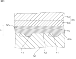
電極層40の表面40aは、好ましくは、図3に示すように、高さdが3nm以上の隆起部41を有する。隆起部41の高さdとは、厚さ方向Hにおける、表面40aの平坦面42から隆起部41の頂部までの距離である。電極層40が、3nm以上の有意な高さの隆起部41を有することは、電極層40全体の平均厚さを確保するのに適し、電極層40の平面視における単位面積あたりの自由電子数(キャリア数)を確保するのに適する。電極層40の単位面積あたりの自由電子数が多いほど、太陽光中の熱線に対する電極層40の反射性は高く、従って、熱線に対する調光フィルムXの遮熱性は高い。調光フィルムXにおいて良好な遮熱性を確保する観点から、隆起部41の高さdは、好ましくは4nm以上、更に好ましくは5nm以上である。隆起部41の高さdは、電極層40の抵抗値の上昇を抑制する観点から、好ましくは20nm以下、より好ましくは10nm以下、更に好ましくは8nm以下である。
As shown in FIG. 3, the
電極層40の厚さは、隆起部41を形成する観点から、好ましくは30nm以上、より好ましくは50nm以上、更に好ましくは70nm以上、一層好ましくは90nm以上、特に好ましくは100nm以上である。電極層40の厚さとは、厚さ方向Hにおける、電極層40の基材フィルム50側表面から平坦面42までの距離とする。電極層40が厚い方ほど、後述の結晶化工程において透明導電層の結晶粒が大きく成長しやすく、従って、電極層40の表面40aにおいて隆起部41を形成しやすい。また、電極層40が厚いことは、電極層40の低抵抗化の観点からも好ましい。電極層40の厚さは、調光フィルムXの耐屈曲性(屈曲時の電極層40の割れの抑制等)を確保する観点から、好ましくは300nm以下、より好ましくは200nm以下、更に好ましくは150nm以下、一層好ましくは120nm以下である。
The thickness of the
電極層40の平面視における自由電子数(キャリア数)は、電極層40での遮熱性確保の観点から、好ましくは5×10¹⁵/cm2以上、より好ましくは8×1015/cm2以上、更に好ましくは10×1015/cm2以上、一層好ましくは11×1015/cm2以上である。電極層40の平面視における自由電子数(キャリア数)は、電極層40の可視光透過率を確保する観点から、好ましくは100×1015/cm2以下、より好ましくは60×1015/cm2以下、更に好ましくは40×1015/cm2以下である。
The number of free electrons (number of carriers) in the
電極層40の可視光透過率は、調光フィルムの透明状態に求められる透明性を調光フィルムXにおいて確保する観点から、例えば50%以上であり、好ましくは70%以上、より好ましくは80%以上、更に好ましくは85%以上である。また、電極層40の可視光透過率は、例えば100%以下である。
The visible light transmittance of the
調光フィルムXの可視光透過率(透明状態時)は、調光フィルムXの透明性を確保する観点から、好ましくは70%以上、より好ましくは80%以上、更に好ましくは85%以上である。基材フィルム10の可視光透過率は、例えば100%以下である。
The visible light transmittance (in a transparent state) of the light control film X is preferably 70% or more, more preferably 80% or more, and even more preferably 85% or more, from the viewpoint of ensuring the transparency of the light control film X. The visible light transmittance of the
調光フィルムXの、波長800nm~1300nmでの平均透過率は、調光フィルムXにおいて、太陽光に対する良好な遮熱性を確保する観点から、好ましくは50%以下、より好ましくは40%以下、更に好ましくは30%以下である。調光フィルムXの同平均透過率は、例えば0%以上であり、好ましくは10%以下である。調光フィルムXは、好ましくは、有色状態または透明状態にてこのような平均透過率(波長800nm~1300nm)の値をとり、より好ましくは、有色状態および透明状態の両状態にてこのような平均透過率(波長800nm~1300nm)の値をとる。 The average transmittance of the light-control film X at wavelengths of 800 nm to 1300 nm is preferably 50% or less, more preferably 40% or less, and even more preferably 30% or less, from the viewpoint of ensuring good heat shielding properties against sunlight in the light-control film X. The average transmittance of the light-control film X is, for example, 0% or more, and preferably 10% or less. The light-control film X preferably has such an average transmittance (wavelengths of 800 nm to 1300 nm) in the colored state or the transparent state, and more preferably has such an average transmittance (wavelengths of 800 nm to 1300 nm) in both the colored state and the transparent state.
調光フィルムXは、例えば以下のように製造される。 The light control film X is manufactured, for example, as follows.
まず、図4Aに示すように、基材フィルム10を用意する。基材フィルム10は、樹脂フィルム11上に硬化樹脂層12を形成することによって作製できる。硬化樹脂層12は、樹脂フィルム11上に、上述の第1硬化型樹脂組成物を塗布して塗膜を形成した後、この塗膜を硬化させることによって形成できる。第1硬化型樹脂組成物が熱硬化型樹脂を含有する場合には、加熱によって前記塗膜を硬化させる。第1硬化型樹脂組成物が紫外線化型樹脂を含有する場合には、紫外線照射によって前記塗膜を硬化させる。樹脂フィルム11上に形成された硬化樹脂層12の露出表面は、必要に応じて、表面改質処理される。表面改質処理としてプラズマ処理する場合、不活性ガスとして例えばアルゴンガスを用いる。また、プラズマ処理における放電電力は、例えば10W以上であり、また、例えば5000W以下である。
First, as shown in FIG. 4A, a
次に、図4Bに示すように、基材フィルム10上に、非晶質の透明導電層20’を形成する(透明導電層形成工程)。具体的には、スパッタリング法により、基材フィルム10における硬化樹脂層12上に透明導電材料を成膜して透明導電層20’を形成する。
Next, as shown in FIG. 4B, an amorphous transparent conductive layer 20' is formed on the base film 10 (transparent conductive layer forming process). Specifically, a transparent conductive material is deposited on the cured
スパッタリング法では、ロールトゥロール方式で成膜プロセスを実施できるスパッタ成膜装置を使用するのが好ましい。調光フィルムXの製造において、ロールトゥロール方式のスパッタ成膜装置を使用する場合、長尺の基材フィルム10を、装置が備える繰出しロールから巻取りロールまで走行させつつ、当該基材フィルム10上に材料を成膜して透明導電層20’を形成する。また、当該スパッタリング法では、一つの成膜室を備えるスパッタ成膜装置を使用してもよいし、基材フィルム10の走行経路に沿って順に配置された複数の成膜室を備えるスパッタ成膜装置を使用してもよい。
In the sputtering method, it is preferable to use a sputtering deposition device capable of performing the deposition process by a roll-to-roll method. When using a roll-to-roll sputtering deposition device in the manufacture of the light-control film X, a material is deposited on the
スパッタリング法では、具体的には、スパッタ成膜装置が備える成膜室内に真空条件下でスパッタリングガス(不活性ガス)を導入しつつ、成膜室内のカソード上に配置されたターゲットにマイナスの電圧を印加する。これにより、グロー放電を発生させてガス原子をイオン化し、当該ガスイオンを高速でターゲット表面に衝突させ、ターゲット表面からターゲット材料を弾き出し、弾き出たターゲット材料を基材フィルム10上に堆積させる。ターゲットの材料としては、例えば、電極層20に関して上述した導電性酸化物の焼結体が用いられる。
Specifically, in the sputtering method, a sputtering gas (inert gas) is introduced under vacuum conditions into a deposition chamber equipped with a sputter deposition apparatus, while a negative voltage is applied to a target placed on a cathode in the deposition chamber. This generates a glow discharge to ionize gas atoms, and the gas ions collide with the target surface at high speed, ejecting the target material from the target surface, and the ejected target material is deposited on the
スパッタリング法は、好ましくは、反応性スパッタリング法である。反応性スパッタリング法では、例えば、スパッタリングガス(不活性ガス)と反応性ガスとしての酸素が、成膜室内に導入される。反応性スパッタリング法において成膜室に導入されるスパッタリングガスおよび酸素の合計導入量に対する、酸素の導入量の割合は、例えば0.01流量%以上であり、また、例えば15流量%以下である。 The sputtering method is preferably a reactive sputtering method. In the reactive sputtering method, for example, a sputtering gas (inert gas) and oxygen as a reactive gas are introduced into the film formation chamber. In the reactive sputtering method, the ratio of the amount of oxygen introduced to the total amount of sputtering gas and oxygen introduced into the film formation chamber is, for example, 0.01 flow rate% or more, and, for example, 15 flow rate% or less.
スパッタリング法による成膜(スパッタ成膜)中の成膜室内の気圧は、例えば0.02Pa以上であり、また、例えば1Pa以下である。 The air pressure in the deposition chamber during deposition by sputtering (sputter deposition) is, for example, 0.02 Pa or more and, for example, 1 Pa or less.
スパッタリング法における成膜温度(スパッタ成膜中の基材フィルム10の温度)は、次の結晶化工程で結晶成長できる非晶質の透明導電層を適切に形成する観点から、好ましくは50℃以下、より好ましくは30℃以下、更に好ましくは10℃以下、一層好ましくは0℃以下、より一層好ましくは-5℃以下である。成膜温度は、例えば、-30℃以上または-20℃以上である。
The film formation temperature in the sputtering method (the temperature of the
ターゲットに対する電圧印加のための電源としては、例えば、DC電源、AC電源、MF電源、およびRF電源が挙げられる。電源としては、DC電源とRF電源とを併用してもよい。スパッタ成膜中の放電電圧の絶対値は、例えば50V以上であり、また、例えば500V以下である。ターゲット上の水平磁場強度は、例えば10mT以上であり、また、例えば100mT以下である。 Examples of power sources for applying voltage to the target include DC power sources, AC power sources, MF power sources, and RF power sources. A DC power source and an RF power source may be used in combination as the power source. The absolute value of the discharge voltage during sputtering deposition is, for example, 50 V or more and, for example, 500 V or less. The horizontal magnetic field strength on the target is, for example, 10 mT or more and, for example, 100 mT or less.
次に、図4Cに示すように、基材フィルム10上の透明導電層20’(図4B)を加熱によって結晶化させて、電極層20(結晶質の透明導電層)を形成する(結晶化工程)。これにより、電極付き基材フィルムY1が作製される。加熱の手段としては、例えば、赤外線ヒーターおよびオーブン(熱媒加熱式オーブン,熱風加熱式オーブン)が挙げられる。加熱温度は、高い結晶化速度を確保する観点から、好ましくは100℃以上、より好ましくは120℃以上である。加熱温度は、基材フィルム10への加熱の影響を抑制する観点から、好ましくは200℃以下、より好ましくは170℃以下、更に好ましくは150℃以下である。加熱時間は、例えば600分未満、好ましくは120分未満、より好ましくは90分以下、更に好ましくは60分以下であり、また、例えば1分以上、好ましくは5分以上である。
Next, as shown in FIG. 4C, the transparent conductive layer 20' (FIG. 4B) on the
次に、図4Dに示すように、電極層20上に調光層30を形成する。調光層30を形成する材料として無機EC材料を用いる場合、例えば、ドライコーティング法によって無機EC材料を電極層20上に成膜する。ドライコーティング法としては、スパッタリング法が好ましい。調光層30を形成する材料として有機EC材料を用いる場合、例えば、ウェットコーティング法によって有機EC材料を電極層20上に成膜する。
Next, as shown in FIG. 4D, the dimming
一方、電極付き基材フィルムY2(基材フィルム50,電極層40)を作製する。具体的には、電極付き基材フィルムY1の作製方法(図4A~図4C)と同様である。
On the other hand, the electrode-attached substrate film Y2 (
次に、図5Aおよび図5Bに示すように、調光層30を伴う電極付き基材フィルムY1と電極付き基材フィルムY2とを一体化させた。具体的には、電極付き基材フィルムY1,Y2によって調光層30を挟まれるように、電極付き基材フィルムY1,Y2および調光層30を一体化させた。
Next, as shown in Figures 5A and 5B, the electrode-attached substrate film Y1 with the light-adjusting
以上のようにして、調光フィルムXを製造できる。調光フィルムXにおいては、電極層20,40間の電圧のオン・オフにより、調光層30が、非透明状態(遮光状態)と透明状態(非遮光状態)との間で切り替えられる。このような調光フィルムXが貼り合わされた窓ガラスでは、電極層20,40間の電圧のオン・オフにより、当該調光フィルムX付き窓ガラスに対する可視光などの光の透過率が、切り替えられる。
In this manner, the light-control film X can be manufactured. In the light-control film X, the light-
調光フィルムXは、上述のように、電極層20における調光層30側の表面20aが、高さ3nm以上の隆起部21を有する。電極層20が、3nm以上の有意な高さの隆起部21を有することは、電極層20全体の平均厚さを確保するのに適する。このような電極層20を有する調光フィルムXは、上述のように、電極層20の平面視における単位面積あたりの自由電子数(キャリア数)を確保するのに適する。電極層20における当該自由電子数が多いほど、太陽光中の熱線に対する電極層20の反射性は高く、従って、調光フィルムXの遮熱性は高い。したがって、調光フィルムXは、太陽光に対する良好な遮熱性を実現するのに適する。このような調光フィルムXは、屋外向け調光フィルムとして好適である。屋外向け調光フィルムとしては、例えば、自家用車等の車のサンルーフ用の調光フィルム、家屋およびビル等の建物の窓用の調光フィルムが挙げられる。
As described above, the light-controlling film X has a raised
調光フィルムXは、上述のように、電極層40における調光層30側の表面40aが、高さ3nm以上の隆起部41を有するのが好ましい。電極層40が、3nm以上の有意な高さの隆起部41を有することは、調光フィルムXにおいて、太陽光に対する良好な遮熱性を実現するのに役立つ。
As described above, the light-control film X preferably has a
本発明について、以下に実施例を示して具体的に説明する。ただし、本発明は、実施例に限定されない。また、以下に記載されている配合量(含有量)、物性値、パラメータなどの具体的数値は、上述の「発明を実施するための形態」において記載されている、それらに対応する配合量(含有量)、物性値、パラメータなどの上限(「以下」または「未満」として定義されている数値)または下限(「以上」または「超える」として定義されている数値)に代替できる。 The present invention will be specifically described below with reference to examples. However, the present invention is not limited to the examples. Furthermore, the specific numerical values of the compounding amounts (contents), physical properties, parameters, etc. described below can be replaced with the upper limit (a numerical value defined as "equal to or less than") or lower limit (a numerical value defined as "equal to or more than") of the corresponding compounding amounts (contents), physical properties, parameters, etc. described in the above-mentioned "Form for carrying out the invention."
〔実施例1〕
まず、長尺の樹脂フィルムとしてのポリエチレンテレフタレート(PET)フィルム(厚さ100μm,三菱ケミカル社製)のロールを用意した。次に、PETフィルムの一方面(第1面)に、熱硬化型の樹脂組成物C1を塗布して塗膜を形成した。樹脂組成物C1は、100質量部のメラミン樹脂と、100質量部のアルキド樹脂と、50質量部の有機シラン縮合物とを含む。次に、PETフィルム上の塗膜を、加熱して熱硬化させた。加熱温度は185℃である。加熱時間は1分である。これにより、厚さ35nmの光学調整層としての第1硬化樹脂層を形成した。次に、PETフィルムの他方面(第2面)に、紫外線硬化型の樹脂組成物C2を塗布して塗膜を形成した。次に、紫外線照射によって当該塗膜を硬化させた。これにより、厚さ2nmのハードコート(HC)層としての第2硬化樹脂層を形成した。以上のようにして、基材フィルム(第1硬化樹脂層/基材フィルム/第2硬化樹脂層)を作製した。
Example 1
First, a roll of polyethylene terephthalate (PET) film (thickness 100 μm, manufactured by Mitsubishi Chemical Corporation) was prepared as a long resin film. Next, a thermosetting resin composition C1 was applied to one side (first surface) of the PET film to form a coating film. The resin composition C1 contains 100 parts by mass of melamine resin, 100 parts by mass of alkyd resin, and 50 parts by mass of an organic silane condensate. Next, the coating film on the PET film was heated and thermoset. The heating temperature was 185° C. The heating time was 1 minute. As a result, a first cured resin layer was formed as an optical adjustment layer having a thickness of 35 nm. Next, a UV-curable resin composition C2 was applied to the other side (second surface) of the PET film to form a coating film. Next, the coating film was cured by UV irradiation. As a result, a second cured resin layer was formed as a hard coat (HC) layer having a thickness of 2 nm. In this manner, a base film (first cured resin layer/base film/second cured resin layer) was produced.
次に、反応性スパッタリング法により、基材フィルムにおける第1硬化樹脂層上に、厚さ105nmの非晶質の透明導電層を形成した(透明導電層形成工程)。本工程では、ロールトゥロール方式のスパッタ成膜装置(DCマグネトロンスパッタ成膜装置)を使用した。同装置は、ロールトゥロール方式でワークフィルムを走行させつつ成膜プロセスを実施できる成膜室を備える。本工程におけるスパッタ成膜の条件は、次のとおりである。 Next, a 105 nm thick amorphous transparent conductive layer was formed on the first cured resin layer of the substrate film by reactive sputtering (transparent conductive layer formation process). In this process, a roll-to-roll sputter deposition device (DC magnetron sputter deposition device) was used. This device is equipped with a deposition chamber that can perform the deposition process while running the work film by the roll-to-roll method. The sputter deposition conditions in this process are as follows:
スパッタ成膜においては、成膜室内の到達真空度が0.6×10⁻⁴Paに至るまでスパッタ成膜装置内を真空排気した後、成膜室内に、スパッタリングガス(不活性ガス)としてのアルゴン(Ar)と、反応性ガスとしての酸素とを導入し、成膜室内の気圧を0.4Paとした。成膜室に導入されるアルゴンおよび酸素の合計導入量に対する酸素導入量の割合は約2.6流量%とした。また、ターゲット(第1ターゲット)としては、酸化インジウムと酸化スズとの焼結体(酸化スズ濃度が10質量%のITO)を用いた。ターゲットに対する電圧印加のための電源としては、DC電源を用いた。ターゲット上の水平磁場強度は90mTとした。成膜温度(透明導電層が積層される基材フィルムの温度)は-8℃とした。 In the sputtering deposition, the sputtering deposition apparatus was evacuated until the ultimate vacuum in the deposition chamber reached 0.6×10 −4 Pa, and then argon (Ar) as a sputtering gas (inert gas) and oxygen as a reactive gas were introduced into the deposition chamber, and the pressure in the deposition chamber was set to 0.4 Pa. The ratio of the amount of oxygen introduced to the total amount of argon and oxygen introduced into the deposition chamber was set to about 2.6 flow %. In addition, a sintered body of indium oxide and tin oxide (ITO with a tin oxide concentration of 10 mass %) was used as the target (first target). A DC power supply was used as the power supply for applying a voltage to the target. The horizontal magnetic field strength above the target was 90 mT. The deposition temperature (the temperature of the substrate film on which the transparent conductive layer is laminated) was set to −8° C.
次に、非晶質の透明導電層を、熱風オーブン内での加熱によって結晶化させた(結晶化工程)。加熱温度は140℃とした。加熱時間は1時間とした。これにより、厚さ105nmの結晶質の透明導電層を電極層として形成した。 Next, the amorphous transparent conductive layer was crystallized by heating in a hot air oven (crystallization process). The heating temperature was 140°C. The heating time was 1 hour. As a result, a crystalline transparent conductive layer with a thickness of 105 nm was formed as an electrode layer.
以上のようにして、電極層付フィルムのロールを作製した。この電極層付フィルムは、基材フィルム(第2硬化樹脂層/樹脂フィルム/第1硬化樹脂層)と、基材フィルム上の電極層とを備える。 In this manner, a roll of film with an electrode layer was produced. This film with an electrode layer comprises a base film (second cured resin layer/resin film/first cured resin layer) and an electrode layer on the base film.
次に、電極層付フィルムのロールから、2枚の電極層付フィルムを切り出した。次に、一方の電極層付フィルム(第1の電極層付フィルム)における電極層上に、粘着剤(品名「LUCIACS CS9861UA」,日東電工社製)を塗付することにより、疑似調光層として厚さ25μmの粘着剤層を形成した。次に、他方の電極層付フィルム(第2の電極層付フィルム)の電極層側を粘着剤層に貼り合わせた。すなわち、2枚の電極層付フィルムを、粘着剤層を介して接合した。 Next, two sheets of electrode layer-attached film were cut out from the roll of electrode layer-attached film. Next, an adhesive (product name "LUCIACS CS9861UA", manufactured by Nitto Denko Corporation) was applied onto the electrode layer of one of the electrode layer-attached films (first electrode layer-attached film) to form an adhesive layer with a thickness of 25 μm as a pseudo-dimming layer. Next, the electrode layer side of the other electrode layer-attached film (second electrode layer-attached film) was attached to the adhesive layer. In other words, the two electrode layer-attached films were joined via the adhesive layer.
以上のようにして、実施例1の積層フィルムを作製した。この積層フィルムは、調光フィルム類似の積層構成を有する疑似調光フィルムである(このフィルムは、疑似的な形態を有するフィルムであり、調光機能を有しない)。実施例1の積層フィルムは、具体的には、第1の基材フィルムと、厚さ105nmの第1の電極層と、疑似調光層と、厚さ105nmの第2の電極層と、第2の基材フィルムとを、厚さ方向にこの順で有する。 In this manner, the laminated film of Example 1 was produced. This laminated film is a pseudo-light-control film with a laminated structure similar to that of a light-control film (this film has a pseudo shape and does not have a light-control function). Specifically, the laminated film of Example 1 has a first substrate film, a first electrode layer with a thickness of 105 nm, a pseudo-light-control layer, a second electrode layer with a thickness of 105 nm, and a second substrate film, in this order in the thickness direction.
〔比較例1〕
透明導電層形成工程以外は、実施例1の積層フィルムと同様にして、比較例1の積層フィルムを作製した。
Comparative Example 1
A laminated film of Comparative Example 1 was produced in the same manner as the laminated film of Example 1, except for the transparent conductive layer formation step.
本比較例における透明導電層工程では、反応性スパッタリング法により、基材フィルムにおける第1硬化樹脂層上に、非晶質の透明導電層の第1層(厚さ11nm)を形成し、続いて、非晶質の透明導電層の第2層(厚さ11nm)を第1層上に形成した。本工程では、ロールトゥロール方式のスパッタ成膜装置(DCマグネトロンスパッタ成膜装置)を使用した。同装置は、ロールトゥロール方式でワークフィルムを走行させつつ成膜プロセスを実施できる第1成膜室および第2成膜室を備える。 In the transparent conductive layer process in this comparative example, a first layer (11 nm thick) of an amorphous transparent conductive layer was formed on the first cured resin layer of the substrate film by reactive sputtering, and then a second layer (11 nm thick) of an amorphous transparent conductive layer was formed on the first layer. In this process, a roll-to-roll sputtering deposition device (DC magnetron sputtering deposition device) was used. The device is equipped with a first deposition chamber and a second deposition chamber that can perform the deposition process while running the work film by the roll-to-roll method.
第1成膜室でのスパッタ成膜の条件は、成膜温度を-8℃に代えて80℃としたこと以外は、実施例1におけるスパッタ成膜での上記条件と同様である。 The conditions for sputter deposition in the first deposition chamber were the same as those for sputter deposition in Example 1, except that the deposition temperature was 80°C instead of -8°C.
第2成膜室でのスパッタ成膜の条件は、次のこと以外は、実施例1におけるスパッタ成膜での上記条件と同様である。成膜温度を-8℃に代えて80℃とした。ターゲットとして、第1ターゲットに代えて第2ターゲットを用いた。第2ターゲットは、酸化インジウムと酸化スズとの焼結体であって、酸化スズ濃度が3質量%のITOである。 The conditions for sputter deposition in the second deposition chamber were the same as those for sputter deposition in Example 1, except for the following: The deposition temperature was 80°C instead of -8°C. The second target was used instead of the first target. The second target was a sintered body of indium oxide and tin oxide, and was ITO with a tin oxide concentration of 3% by mass.
比較例1の積層フィルムは、第1の基材フィルムと、厚さ22nmの第1の電極層と、疑似調光層と、厚さ22nmの第2の電極層と、第2の基材フィルムとを、厚さ方向にこの順で有する。 The laminated film of Comparative Example 1 has a first base film, a first electrode layer having a thickness of 22 nm, a pseudo-switching layer, a second electrode layer having a thickness of 22 nm, and a second base film, in that order in the thickness direction.
〈電極層の厚さ〉
実施例1および比較例1の各積層フィルムの作製過程で得られた電極層付フィルムの電極層の厚さを、電界放射型透過電子顕微鏡(FE-TEM)での観察により測定した。具体的には、まず、FIB(Focused Ion Beam)加工により、実施例1および比較例1における各電極層の断面観察用サンプル(第1サンプル)を作製した(FIBマイクロサンプリング法)。FIBマイクロサンプリング法では、FIB装置(品名「FB2200」,Hitachi製)を使用し、加速電圧を10kVとした。次に、第1サンプルにおける電極層の断面をFE-TEMによって観察し、当該観察画像において電極層の厚さを測定した。同観察では、FE-TEM装置(品名「JEM-2800」,JEOL製)を使用し、加速電圧を200kVとした。
<Thickness of electrode layer>
The thickness of the electrode layer of the electrode layer-attached film obtained in the process of producing each laminated film of Example 1 and Comparative Example 1 was measured by observation with a field emission transmission electron microscope (FE-TEM). Specifically, first, a sample for cross-sectional observation of each electrode layer in Example 1 and Comparative Example 1 (first sample) was produced by FIB (Focused Ion Beam) processing (FIB microsampling method). In the FIB microsampling method, an FIB device (product name "FB2200", manufactured by Hitachi) was used, and the acceleration voltage was set to 10 kV. Next, the cross section of the electrode layer in the first sample was observed by FE-TEM, and the thickness of the electrode layer was measured in the observed image. In the observation, an FE-TEM device (product name "JEM-2800", manufactured by JEOL) was used, and the acceleration voltage was set to 200 kV.
比較例1における電極層の第1層の厚さは、当該第1層の上に第2層を形成する前の中間作製物から断面観察用サンプルを作製し、当該サンプルのFE-TEM観察により測定した。比較例1における電極層の第2層の厚さは、比較例1における電極層の総厚から第1層の厚さを差し引いて求めた。 The thickness of the first layer of the electrode layer in Comparative Example 1 was measured by preparing a cross-sectional observation sample from the intermediate product before the second layer was formed on the first layer and observing the sample with an FE-TEM. The thickness of the second layer of the electrode layer in Comparative Example 1 was determined by subtracting the thickness of the first layer from the total thickness of the electrode layer in Comparative Example 1.
〈隆起部の観察〉
実施例1および比較例1の各積層フィルムの作製過程で得られた電極層付フィルムの電極層について、表面(基材フィルムとは反対側の表面)の隆起部の有無を確認した。
Observation of the protuberance
For the electrode layer of the electrode layer-attached film obtained in the process of producing each of the laminated films of Example 1 and Comparative Example 1, the presence or absence of a protrusion on the surface (the surface opposite to the base film) was confirmed.
まず、FIB(Focused Ion Beam)加工により、電極層表面の断面形状を観察可能な断面観察用サンプル(第2サンプル)を作製した。第2サンプルの作成方法は、上述の第1サンプルの作製方法と同様である。次に、第2サンプルにおける電極層の断面をFE-TEMによって観察し、当該観察画像において電極層の表面の隆起部の有無を確認した。同観察では、FE-TEM装置(品名「JEM-2800」,JEOL製)を使用し、加速電圧を200kVとした。実施例1における電極層付フィルムでは、電極層表面に隆起部を確認できた。比較例1における電極層付フィルムでは、電極層表面に隆起部を確認できなかった。また、実施例1における電極層付フィルムの観察画像においては、観察視野に含まれる各隆起部(周りの平坦面から突き出る形状を有する隆起部)の高さを測定した。隆起部の高さとは、電極層の厚さ方向における平坦面から隆起部の頂部までの距離である。そして、任意に選択された10個の高さ3nm以上の隆起部の高さの平均値を求めた。その値を、隆起部高さとして表1に示す。比較例1の積層フィルムの電極層は、それぞれが比較的薄い透明導電層(第1層および第2層)が積み重ねられた構成を有すること、また、比較的高温で成膜されたものであることから、高さ3nm以上の隆起部を有しない、と考えられる。 First, a cross-sectional observation sample (second sample) capable of observing the cross-sectional shape of the electrode layer surface was prepared by FIB (Focused Ion Beam) processing. The method for preparing the second sample was the same as that for the first sample described above. Next, the cross-section of the electrode layer in the second sample was observed by FE-TEM, and the presence or absence of protrusions on the surface of the electrode layer was confirmed in the observation image. In the observation, a FE-TEM device (product name "JEM-2800", manufactured by JEOL) was used, and the acceleration voltage was set to 200 kV. In the film with electrode layer in Example 1, protrusions could be confirmed on the surface of the electrode layer. In the film with electrode layer in Comparative Example 1, protrusions could not be confirmed on the surface of the electrode layer. In the observation image of the film with electrode layer in Example 1, the height of each protrusion (protrusion having a shape protruding from the surrounding flat surface) included in the observation field was measured. The height of the protrusion is the distance from the flat surface to the top of the protrusion in the thickness direction of the electrode layer. The average height of 10 randomly selected protrusions with a height of 3 nm or more was then calculated. The average value is shown in Table 1 as the protrusion height. The electrode layer of the laminated film of Comparative Example 1 is composed of relatively thin transparent conductive layers (first and second layers) stacked on top of each other, and is formed at a relatively high temperature, so it is believed that it does not have protrusions with a height of 3 nm or more.
〈透過率,反射率〉
実施例1および比較例1の各積層フィルムについて、分光光度計U-4100(HITACHI社製)により、波長300nm~2500nmの範囲における日射透過率(Te)および日射反射率(Re)を測定した。本測定では、測定ピッチを5nmとした。測定結果を表1に示す。日射とは、波長300~2500nmの範囲の放射をいう。日射透過率(Te)は、分光透過率と分光日射照度とを式中に含む所定の積和計算から、分光光度計によって算出される。日射反射率(Re)は、分光反射率と分光日射照度とを式中に含む所定の積和計算から、分光光度計によって算出される。
<Transmittance, reflectance>
For each laminate film of Example 1 and Comparative Example 1, the solar transmittance (Te) and solar reflectance (Re) in the wavelength range of 300 nm to 2500 nm were measured using a spectrophotometer U-4100 (manufactured by Hitachi Corporation). In this measurement, the measurement interval was 5 nm. The measurement results are shown in Table 1. Solar radiation refers to radiation in the wavelength range of 300 to 2500 nm. The solar transmittance (Te) is calculated by the spectrophotometer from a predetermined product-sum calculation that includes the spectral transmittance and the spectral solar irradiance in the formula. The solar reflectance (Re) is calculated by the spectrophotometer from a predetermined product-sum calculation that includes the spectral reflectance and the spectral solar irradiance in the formula.
〈日射熱取得率〉
実施例1および比較例1の各積層フィルムについて、日射熱取得率を求めた。具体的には、積層フィルムの日射熱取得率を、ISO 13837:2021に基づき、下記の式(1)~(3)によって求めた。式(1)において、Ttsは、日射熱取得率を表し、遮熱性の指標となる。
<Solar heat gain coefficient>
The solar heat gain coefficient was determined for each of the laminate films of Example 1 and Comparative Example 1. Specifically, the solar heat gain coefficient of the laminate film was determined by the following formulas (1) to (3) based on ISO 13837:2021. In formula (1), Tts represents the solar heat gain coefficient and is an index of heat shielding properties.
Tts = Te + Qi (1)
Qi = Ae ×{hi/(hi + he)} (2)
Ae = 100- Te - Re (3)
Tts = Te + Qi (1)
Qi = Ae × {hi/(hi + he)} (2)
Ae = 100- Te - Re (3)
実施例1および比較例1の各積層フィルムにとり、式(1)~(3)については以下のとおりである。Ttsは、試料に(積層フィルム)に対して照射される光(照射光)の総エネルギーを100%とした場合の、当該試料を通過するエネルギーの合計の割合(%)を示す。Teは、試料に対する照射光のうち当該試料を透過する光(透過光)のエネルギーを、割合で示す。Teとして、上記測定で得られた日射透過率を用いた。Qiは、試料を通過する二次熱流速を表し、式(2)によって求められる。この値が小さいほど、試料は熱を伝えにくく、断熱性が高いことを意味する。式(2)において、Aeは、試料に対する照射光のエネルギーのうち当該試料によって吸収されるエネルギーを割合で示し、式(3)によって求められる。hiは、試料における、光通過方向と同方向への熱の伝わりやすさを示すパラメータである。hiとして8W/(m2・K)を用いた。heは、試料における、光通過方向とは逆の方向への熱の伝わりやすさを示すパラメータである。heとして21W/(m2・K)を用いた。式(3)において、Reは、試料に対する照射光のうち当該試料にて反射される光(反射光)のエネルギーを、割合で示す。Reとして、上記測定で得られた日射反射率を用いた。 For each laminated film of Example 1 and Comparative Example 1, formulas (1) to (3) are as follows. Tts indicates the percentage (%) of the total energy passing through the sample when the total energy of the light (irradiated light) irradiated to the sample (laminated film) is 100%. Te indicates the percentage of the energy of the light (transmitted light) that passes through the sample of the light irradiated to the sample. The solar transmittance obtained by the above measurement was used as Te. Qi represents the secondary heat flow rate passing through the sample and is calculated by formula (2). The smaller this value, the less heat is transmitted to the sample and the higher the thermal insulation. In formula (2), Ae indicates the percentage of the energy absorbed by the sample out of the energy of the light irradiated to the sample and is calculated by formula (3). h is a parameter that indicates the ease of heat transmission in the same direction as the light passing direction in the sample. 8 W/( m2 ·K) was used as h. he is a parameter indicating the ease of heat transfer in the sample in the direction opposite to the light transmission direction. 21 W/( m2 ·K) was used as he. In formula (3), Re indicates the ratio of the energy of the light reflected by the sample (reflected light) to the light irradiated to the sample. The solar reflectance obtained in the above measurement was used as Re.
〈キャリア数〉
実施例1および比較例1における各電極層のキャリア数を、ホール効果測定装置(品名「HL5500PC」,バイオラッド社製)によって測定した。測定結果を表1に示す。
Number of careers
The number of carriers in each electrode layer in Example 1 and Comparative Example 1 was measured using a Hall effect measuring device (product name "HL5500PC", manufactured by Bio-Rad Laboratories). The measurement results are shown in Table 1.
X 調光フィルム
Y1,Y2 電極付き基材フィルム
10 基材フィルム
11 樹脂フィルム
20 電極層(第1電極層)
20a,40a 表面
21,41 隆起部
30 調光層
40 電極層(第2電極層)
X light control films Y1, Y2 electrode-attached
20a,
Claims (4)
前記第1電極層における前記調光層の側の表面が、高さ3nm以上、8nm以下の隆起部を有し、
前記第1電極層の厚さが、30nm以上である、調光フィルム。 A light-controlling film including a base film, a first electrode layer, a light-controlling layer, and a second electrode layer in this order in a thickness direction,
the surface of the first electrode layer on the side of the light-controlling layer has a protrusion having a height of 3 nm or more and 8 nm or less ;
A light-controlling film, wherein the first electrode layer has a thickness of 30 nm or more.
Priority Applications (8)
| Application Number | Priority Date | Filing Date | Title |
|---|---|---|---|
| JP2023017382A JP7581396B2 (en) | 2023-02-08 | 2023-02-08 | Light control film |
| CN202480010735.4A CN120641817A (en) | 2023-02-08 | 2024-01-24 | dimming film |
| KR1020240010927A KR20240124201A (en) | 2023-02-08 | 2024-01-24 | Light control film |
| PCT/JP2024/002010 WO2024166684A1 (en) | 2023-02-08 | 2024-01-24 | Light control film |
| CN202480003469.2A CN119585672A (en) | 2023-02-08 | 2024-01-24 | Dimming film |
| PCT/JP2024/002009 WO2024166683A1 (en) | 2023-02-08 | 2024-01-24 | Light control film |
| KR1020247031958A KR102792308B1 (en) | 2023-02-08 | 2024-01-24 | Dimming film |
| CN202410176700.XA CN118466075A (en) | 2023-02-08 | 2024-02-08 | Dimming film |
Applications Claiming Priority (1)
| Application Number | Priority Date | Filing Date | Title |
|---|---|---|---|
| JP2023017382A JP7581396B2 (en) | 2023-02-08 | 2023-02-08 | Light control film |
Publications (2)
| Publication Number | Publication Date |
|---|---|
| JP2024112408A JP2024112408A (en) | 2024-08-21 |
| JP7581396B2 true JP7581396B2 (en) | 2024-11-12 |
Family
ID=92156732
Family Applications (1)
| Application Number | Title | Priority Date | Filing Date |
|---|---|---|---|
| JP2023017382A Active JP7581396B2 (en) | 2023-02-08 | 2023-02-08 | Light control film |
Country Status (3)
| Country | Link |
|---|---|
| JP (1) | JP7581396B2 (en) |
| KR (1) | KR20240124201A (en) |
| CN (1) | CN118466075A (en) |
Citations (5)
| Publication number | Priority date | Publication date | Assignee | Title |
|---|---|---|---|---|
| JP2019003060A (en) | 2017-06-15 | 2019-01-10 | 国立大学法人千葉大学 | Electrochromic display element |
| JP2020134575A (en) | 2019-02-14 | 2020-08-31 | 凸版印刷株式会社 | Light control body |
| JP2021173825A (en) | 2020-04-22 | 2021-11-01 | 日本放送協会 | Transmittance variable element and manufacturing method thereof |
| WO2022030582A1 (en) | 2020-08-07 | 2022-02-10 | Agc株式会社 | Laminated glass |
| JP2024034702A (en) | 2022-09-01 | 2024-03-13 | Toppanホールディングス株式会社 | light control sheet |
Family Cites Families (1)
| Publication number | Priority date | Publication date | Assignee | Title |
|---|---|---|---|---|
| JP7171181B2 (en) | 2017-12-01 | 2022-11-15 | 日東電工株式会社 | light control film |
-
2023
- 2023-02-08 JP JP2023017382A patent/JP7581396B2/en active Active
-
2024
- 2024-01-24 KR KR1020240010927A patent/KR20240124201A/en active Pending
- 2024-02-08 CN CN202410176700.XA patent/CN118466075A/en active Pending
Patent Citations (5)
| Publication number | Priority date | Publication date | Assignee | Title |
|---|---|---|---|---|
| JP2019003060A (en) | 2017-06-15 | 2019-01-10 | 国立大学法人千葉大学 | Electrochromic display element |
| JP2020134575A (en) | 2019-02-14 | 2020-08-31 | 凸版印刷株式会社 | Light control body |
| JP2021173825A (en) | 2020-04-22 | 2021-11-01 | 日本放送協会 | Transmittance variable element and manufacturing method thereof |
| WO2022030582A1 (en) | 2020-08-07 | 2022-02-10 | Agc株式会社 | Laminated glass |
| JP2024034702A (en) | 2022-09-01 | 2024-03-13 | Toppanホールディングス株式会社 | light control sheet |
Also Published As
| Publication number | Publication date |
|---|---|
| KR20240124201A (en) | 2024-08-16 |
| CN118466075A (en) | 2024-08-09 |
| JP2024112408A (en) | 2024-08-21 |
Similar Documents
| Publication | Publication Date | Title |
|---|---|---|
| JP7278372B2 (en) | transparent conductive film | |
| WO2020031632A1 (en) | Light-transmitting conductive film and light control film | |
| JP7581396B2 (en) | Light control film | |
| JP7561957B1 (en) | Light control film | |
| JP7549117B1 (en) | Light control film | |
| WO2024166684A1 (en) | Light control film | |
| KR102792308B1 (en) | Dimming film | |
| JP7068558B2 (en) | Transparent conductive film | |
| JP7418506B1 (en) | transparent conductive film | |
| KR102695635B1 (en) | Transparent conductive film | |
| JP7784421B2 (en) | Film heaters and heated glass | |
| KR102698069B1 (en) | Transparent electroconductive film | |
| CN111554431A (en) | Conductive Films and Touch Panels | |
| JP7509852B2 (en) | Transparent Conductive Film | |
| JPH02199428A (en) | Light control laminated body | |
| JP3931806B2 (en) | Manufacturing method of electromagnetic wave shielding film for plasma display and front filter for plasma display panel | |
| JP6954444B2 (en) | Transparent conductors, dimmers and electronic devices | |
| JP5895089B1 (en) | Heat ray shielding laminate and window glass using the laminate | |
| WO2025041569A1 (en) | Glass film with near-infrared blocking film, near-infrared blocking film laminate, method for manufacturing glass film with near-infrared blocking film, and method for manufacturing near-infrared blocking film laminate | |
| WO2016199661A1 (en) | Heat-ray-shielding layered body and window glass using heat-ray-shielding layered body |
Legal Events
| Date | Code | Title | Description |
|---|---|---|---|
| A521 | Request for written amendment filed |
Free format text: JAPANESE INTERMEDIATE CODE: A523 Effective date: 20240507 |
|
| A621 | Written request for application examination |
Free format text: JAPANESE INTERMEDIATE CODE: A621 Effective date: 20240507 |
|
| A871 | Explanation of circumstances concerning accelerated examination |
Free format text: JAPANESE INTERMEDIATE CODE: A871 Effective date: 20240507 |
|
| A131 | Notification of reasons for refusal |
Free format text: JAPANESE INTERMEDIATE CODE: A131 Effective date: 20240528 |
|
| A521 | Request for written amendment filed |
Free format text: JAPANESE INTERMEDIATE CODE: A523 Effective date: 20240626 |
|
| A131 | Notification of reasons for refusal |
Free format text: JAPANESE INTERMEDIATE CODE: A131 Effective date: 20240730 |
|
| A521 | Request for written amendment filed |
Free format text: JAPANESE INTERMEDIATE CODE: A523 Effective date: 20240912 |
|
| TRDD | Decision of grant or rejection written | ||
| A01 | Written decision to grant a patent or to grant a registration (utility model) |
Free format text: JAPANESE INTERMEDIATE CODE: A01 Effective date: 20241022 |
|
| A61 | First payment of annual fees (during grant procedure) |
Free format text: JAPANESE INTERMEDIATE CODE: A61 Effective date: 20241030 |
|
| R150 | Certificate of patent or registration of utility model |
Ref document number: 7581396 Country of ref document: JP Free format text: JAPANESE INTERMEDIATE CODE: R150 |