JP7581301B2 - 後面及び/若しくは前面、並びに/又はバルクの欠陥の同時検出 - Google Patents
後面及び/若しくは前面、並びに/又はバルクの欠陥の同時検出 Download PDFInfo
- Publication number
- JP7581301B2 JP7581301B2 JP2022184761A JP2022184761A JP7581301B2 JP 7581301 B2 JP7581301 B2 JP 7581301B2 JP 2022184761 A JP2022184761 A JP 2022184761A JP 2022184761 A JP2022184761 A JP 2022184761A JP 7581301 B2 JP7581301 B2 JP 7581301B2
- Authority
- JP
- Japan
- Prior art keywords
- light
- substrate
- wavelength
- angle
- backscattered light
- Prior art date
- Legal status (The legal status is an assumption and is not a legal conclusion. Google has not performed a legal analysis and makes no representation as to the accuracy of the status listed.)
- Active
Links
Images
Classifications
-
- G—PHYSICS
- G01—MEASURING; TESTING
- G01N—INVESTIGATING OR ANALYSING MATERIALS BY DETERMINING THEIR CHEMICAL OR PHYSICAL PROPERTIES
- G01N21/00—Investigating or analysing materials by the use of optical means, i.e. using sub-millimetre waves, infrared, visible or ultraviolet light
- G01N21/84—Systems specially adapted for particular applications
- G01N21/88—Investigating the presence of flaws or contamination
- G01N21/8806—Specially adapted optical and illumination features
-
- G—PHYSICS
- G01—MEASURING; TESTING
- G01N—INVESTIGATING OR ANALYSING MATERIALS BY DETERMINING THEIR CHEMICAL OR PHYSICAL PROPERTIES
- G01N21/00—Investigating or analysing materials by the use of optical means, i.e. using sub-millimetre waves, infrared, visible or ultraviolet light
- G01N21/84—Systems specially adapted for particular applications
- G01N21/88—Investigating the presence of flaws or contamination
- G01N21/8851—Scan or image signal processing specially adapted therefor, e.g. for scan signal adjustment, for detecting different kinds of defects, for compensating for structures, markings, edges
-
- G—PHYSICS
- G01—MEASURING; TESTING
- G01N—INVESTIGATING OR ANALYSING MATERIALS BY DETERMINING THEIR CHEMICAL OR PHYSICAL PROPERTIES
- G01N21/00—Investigating or analysing materials by the use of optical means, i.e. using sub-millimetre waves, infrared, visible or ultraviolet light
- G01N21/84—Systems specially adapted for particular applications
- G01N21/88—Investigating the presence of flaws or contamination
- G01N21/95—Investigating the presence of flaws or contamination characterised by the material or shape of the object to be examined
- G01N21/9501—Semiconductor wafers
-
- G—PHYSICS
- G06—COMPUTING OR CALCULATING; COUNTING
- G06T—IMAGE DATA PROCESSING OR GENERATION, IN GENERAL
- G06T7/00—Image analysis
- G06T7/0002—Inspection of images, e.g. flaw detection
- G06T7/0004—Industrial image inspection
- G06T7/001—Industrial image inspection using an image reference approach
-
- G—PHYSICS
- G01—MEASURING; TESTING
- G01N—INVESTIGATING OR ANALYSING MATERIALS BY DETERMINING THEIR CHEMICAL OR PHYSICAL PROPERTIES
- G01N21/00—Investigating or analysing materials by the use of optical means, i.e. using sub-millimetre waves, infrared, visible or ultraviolet light
- G01N21/17—Systems in which incident light is modified in accordance with the properties of the material investigated
- G01N21/25—Colour; Spectral properties, i.e. comparison of effect of material on the light at two or more different wavelengths or wavelength bands
- G01N21/31—Investigating relative effect of material at wavelengths characteristic of specific elements or molecules, e.g. atomic absorption spectrometry
- G01N21/314—Investigating relative effect of material at wavelengths characteristic of specific elements or molecules, e.g. atomic absorption spectrometry with comparison of measurements at specific and non-specific wavelengths
- G01N2021/3155—Measuring in two spectral ranges, e.g. UV and visible
-
- G—PHYSICS
- G01—MEASURING; TESTING
- G01N—INVESTIGATING OR ANALYSING MATERIALS BY DETERMINING THEIR CHEMICAL OR PHYSICAL PROPERTIES
- G01N21/00—Investigating or analysing materials by the use of optical means, i.e. using sub-millimetre waves, infrared, visible or ultraviolet light
- G01N21/84—Systems specially adapted for particular applications
- G01N21/88—Investigating the presence of flaws or contamination
- G01N21/8806—Specially adapted optical and illumination features
- G01N2021/8809—Adjustment for highlighting flaws
-
- G—PHYSICS
- G01—MEASURING; TESTING
- G01N—INVESTIGATING OR ANALYSING MATERIALS BY DETERMINING THEIR CHEMICAL OR PHYSICAL PROPERTIES
- G01N21/00—Investigating or analysing materials by the use of optical means, i.e. using sub-millimetre waves, infrared, visible or ultraviolet light
- G01N21/84—Systems specially adapted for particular applications
- G01N21/88—Investigating the presence of flaws or contamination
- G01N21/8806—Specially adapted optical and illumination features
- G01N2021/8822—Dark field detection
- G01N2021/8825—Separate detection of dark field and bright field
-
- G—PHYSICS
- G01—MEASURING; TESTING
- G01N—INVESTIGATING OR ANALYSING MATERIALS BY DETERMINING THEIR CHEMICAL OR PHYSICAL PROPERTIES
- G01N21/00—Investigating or analysing materials by the use of optical means, i.e. using sub-millimetre waves, infrared, visible or ultraviolet light
- G01N21/84—Systems specially adapted for particular applications
- G01N21/88—Investigating the presence of flaws or contamination
- G01N21/8806—Specially adapted optical and illumination features
- G01N2021/8841—Illumination and detection on two sides of object
-
- G—PHYSICS
- G01—MEASURING; TESTING
- G01N—INVESTIGATING OR ANALYSING MATERIALS BY DETERMINING THEIR CHEMICAL OR PHYSICAL PROPERTIES
- G01N21/00—Investigating or analysing materials by the use of optical means, i.e. using sub-millimetre waves, infrared, visible or ultraviolet light
- G01N21/84—Systems specially adapted for particular applications
- G01N21/88—Investigating the presence of flaws or contamination
- G01N21/8806—Specially adapted optical and illumination features
- G01N2021/8845—Multiple wavelengths of illumination or detection
-
- G—PHYSICS
- G01—MEASURING; TESTING
- G01N—INVESTIGATING OR ANALYSING MATERIALS BY DETERMINING THEIR CHEMICAL OR PHYSICAL PROPERTIES
- G01N21/00—Investigating or analysing materials by the use of optical means, i.e. using sub-millimetre waves, infrared, visible or ultraviolet light
- G01N21/84—Systems specially adapted for particular applications
- G01N21/88—Investigating the presence of flaws or contamination
- G01N21/8851—Scan or image signal processing specially adapted therefor, e.g. for scan signal adjustment, for detecting different kinds of defects, for compensating for structures, markings, edges
- G01N2021/8854—Grading and classifying of flaws
- G01N2021/8858—Flaw counting
-
- G—PHYSICS
- G01—MEASURING; TESTING
- G01N—INVESTIGATING OR ANALYSING MATERIALS BY DETERMINING THEIR CHEMICAL OR PHYSICAL PROPERTIES
- G01N21/00—Investigating or analysing materials by the use of optical means, i.e. using sub-millimetre waves, infrared, visible or ultraviolet light
- G01N21/84—Systems specially adapted for particular applications
- G01N21/88—Investigating the presence of flaws or contamination
- G01N21/8851—Scan or image signal processing specially adapted therefor, e.g. for scan signal adjustment, for detecting different kinds of defects, for compensating for structures, markings, edges
- G01N2021/8887—Scan or image signal processing specially adapted therefor, e.g. for scan signal adjustment, for detecting different kinds of defects, for compensating for structures, markings, edges based on image processing techniques
-
- G—PHYSICS
- G01—MEASURING; TESTING
- G01N—INVESTIGATING OR ANALYSING MATERIALS BY DETERMINING THEIR CHEMICAL OR PHYSICAL PROPERTIES
- G01N21/00—Investigating or analysing materials by the use of optical means, i.e. using sub-millimetre waves, infrared, visible or ultraviolet light
- G01N21/17—Systems in which incident light is modified in accordance with the properties of the material investigated
- G01N21/25—Colour; Spectral properties, i.e. comparison of effect of material on the light at two or more different wavelengths or wavelength bands
- G01N21/31—Investigating relative effect of material at wavelengths characteristic of specific elements or molecules, e.g. atomic absorption spectrometry
- G01N21/35—Investigating relative effect of material at wavelengths characteristic of specific elements or molecules, e.g. atomic absorption spectrometry using infrared light
- G01N21/3563—Investigating relative effect of material at wavelengths characteristic of specific elements or molecules, e.g. atomic absorption spectrometry using infrared light for analysing solids; Preparation of samples therefor
-
- G—PHYSICS
- G01—MEASURING; TESTING
- G01N—INVESTIGATING OR ANALYSING MATERIALS BY DETERMINING THEIR CHEMICAL OR PHYSICAL PROPERTIES
- G01N2201/00—Features of devices classified in G01N21/00
- G01N2201/06—Illumination; Optics
- G01N2201/063—Illuminating optical parts
- G01N2201/0636—Reflectors
- G01N2201/0637—Elliptic
-
- G—PHYSICS
- G06—COMPUTING OR CALCULATING; COUNTING
- G06T—IMAGE DATA PROCESSING OR GENERATION, IN GENERAL
- G06T2207/00—Indexing scheme for image analysis or image enhancement
- G06T2207/10—Image acquisition modality
- G06T2207/10141—Special mode during image acquisition
- G06T2207/10152—Varying illumination
-
- G—PHYSICS
- G06—COMPUTING OR CALCULATING; COUNTING
- G06T—IMAGE DATA PROCESSING OR GENERATION, IN GENERAL
- G06T2207/00—Indexing scheme for image analysis or image enhancement
- G06T2207/30—Subject of image; Context of image processing
- G06T2207/30108—Industrial image inspection
- G06T2207/30148—Semiconductor; IC; Wafer
Landscapes
- Physics & Mathematics (AREA)
- General Physics & Mathematics (AREA)
- Biochemistry (AREA)
- General Health & Medical Sciences (AREA)
- Health & Medical Sciences (AREA)
- Life Sciences & Earth Sciences (AREA)
- Chemical & Material Sciences (AREA)
- Analytical Chemistry (AREA)
- Pathology (AREA)
- Immunology (AREA)
- Engineering & Computer Science (AREA)
- Computer Vision & Pattern Recognition (AREA)
- Signal Processing (AREA)
- Quality & Reliability (AREA)
- Theoretical Computer Science (AREA)
- Investigating Materials By The Use Of Optical Means Adapted For Particular Applications (AREA)
- Testing Or Measuring Of Semiconductors Or The Like (AREA)
Description
本出願は、全体が参照により本明細書に組み込まれる、2021年11月18日に出願された「SIMULTANEOUS BACK AND/OR FRONT AND/OR BULK DEFECT DETECTION」と題した米国特許仮出願第63/280,949号に対する35 USC 119の下での優先権を主張するものである。
本開示は、概して、検査システムに関し、特に、サブミクロン感度で後面、前面、及び/又はバルクの欠陥を同時に検出する高スループット基板検査システムに関する。
Claims (15)
- 基板検査のための検査システムであって、前記検査システムが、
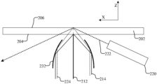
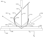
第1の角度で基板に向けられ、前記基板の第1の表面上の第1の場所に集束される第1の波長の光を生成し、前記基板の第1の表面に対して斜角である第2の角度で前記基板に向けられた第2の波長の光を生成する少なくとも1つの照明器と、
前記第2の角度を前記第1の角度とは独立に調整して、前記第2の波長の前記光を、前記第1の表面とは異なる前記基板の第2の表面上の指定された場所に集束させる調整システムと、
前記少なくとも1つの照明器からの前記光に応答して前記基板からの後方散乱光を集める検出光学系と、
第1のスペクトルの前記後方散乱光を受光し、前記第1の表面を表す第1の画像を生成し、第2のスペクトルの前記後方散乱光を受光して前記基板の第2の表面又は前記第2の表面近くを表す第2の画像を生成する少なくとも1つの検出器と、を備える、検査システム。 - 前記基板が、前記第1の波長の前記光に対して不透明であり、前記第2の波長の前記光に対して少なくとも部分的に透明である、請求項1に記載の検査システム。
- 前記検出光学系が、
前記第1の表面からの前記後方散乱光、及び前記第2の表面又は前記第2の表面近くからの前記後方散乱光を集める楕円ミラーであって、前記楕円ミラーが、中を通って前記第2の波長の前記光が前記第2の角度で前記基板に向けられる第1の開口と、中を通って、前記基板によって反射された前記第2の波長の光が前記楕円ミラーを出る第2の開口と、を備えるか、又は前記第2の波長の前記光が、前記楕円ミラーと前記基板の前記第1の表面との間で前記第2の角度で前記基板に向けられる、楕円ミラーと、
前記楕円ミラーによって集められた前記後方散乱光を前記少なくとも1つの検出器に向かって向ける少なくとも1つの折り返しミラーであって、前記少なくとも1つの折り返しミラーが、中を通って前記第1の波長の前記光が前記第1の角度で前記基板に向けられる開口を備える、少なくとも1つの折り返しミラーと、を備える、請求項1に記載の検査システム。 - 前記第1の角度が、前記第1の表面に対して垂直な又は垂直に近い角度であり、前記第2のスペクトルの前記後方散乱光が、前記第2の角度で前記基板に向けられた前記第2の波長の前記光によって生み出される、請求項1に記載の検査システム。
- 前記第1のスペクトルが可視波長を含み、前記第2のスペクトルが赤外波長を含み、前記第1の波長が可視波長であり、前記第2の波長が赤外波長である、請求項1に記載の検査システム。
- 前記少なくとも1つの検出器が、
前記第1のスペクトルの前記後方散乱光を受光する第1の検出器と、
前記第2のスペクトルの前記後方散乱光を受光する第2の検出器と、
前記後方散乱光を受光し、前記第1のスペクトルの前記後方散乱光を前記第1の検出器に向け、前記第2のスペクトルの前記後方散乱光を前記第2の検出器に向ける色フィルタと、を備える、請求項1に記載の検査システム。 - 前記調整システムが、前記第2の角度を調整して、前記第1の場所と共有される前記基板のz軸上にある、前記第2の表面上の前記指定された場所に前記第2の波長の前記光を集束させる、請求項1に記載の検査システム。
- 前記調整システムが、前記第2の角度を調整するためにミラーに結合されたアクチュエータを含む、請求項1に記載の検査システム。
- 前記第1の画像と前記第2の画像との比較に基づいて、前記第1の表面上の欠陥の残留信号について補正された前記基板の前記第2の表面の上又は近くの欠陥を表す第3の画像を生成するプロセッサ、を更に備える、請求項1に記載の検査システム。
- 第1の角度で基板に向けられ、前記基板の第1の表面上の第1の場所に集束される第1の波長の光を生成することと、
前記基板の第1の表面に対して斜角である第2の角度で前記基板に向けられた第2の波長の光を生成することと、
前記第2の波長の前記光を、前記第1の表面とは異なる前記基板の第2の表面上の指定された場所に集束させるように前記第2の角度を前記第1の角度とは独立に調整することと、
前記第1の波長及び前記第2の波長の前記光に応答して、前記基板からの後方散乱光を集めることと、
第1のスペクトルの前記後方散乱光に基づいて、前記第1の表面を表す第1の画像を生成することと、
第2のスペクトルの前記後方散乱光に基づいて、前記基板の第2の表面又は前記第2の表面近くを表す第2の画像を生成することと、を含む、方法。 - 前記基板が、前記第1の波長の前記光に対して不透明であり、前記第2の波長の前記光に対して少なくとも部分的に透明である、請求項10に記載の方法。
- 前記基板からの前記後方散乱光を集めることが、
前記第1の表面からの前記後方散乱光、及び前記第2の表面又は前記第2の表面近くからの前記後方散乱光を、楕円ミラーを用いて受光することであって、前記楕円ミラーが、中を通って前記第2の波長の前記光が前記第2の角度で前記基板に向けられる第1の開口と、中を通って、前記基板によって反射された前記第2の波長の光が前記楕円ミラーを出る第2の開口と、を備えるか、又は前記第2の波長の前記光が、前記楕円ミラーと前記基板の前記第1の表面との間で前記第2の角度で前記基板に向けられることと、
中を通って前記第1の波長の前記光が前記第1の角度で前記基板に向けられる開口を備える少なくとも1つの折り返しミラーを用いて、前記楕円ミラーによって集められた前記後方散乱光を少なくとも1つの検出器に向かって向けることと、を含む、請求項10に記載の方法。 - 前記第1の角度が、前記第1の表面に対して垂直な又は垂直に近い角度であり、前記第1の波長が可視波長であり、前記第2の波長が赤外波長であり、前記第2のスペクトルの前記後方散乱光が、前記第2の角度で前記基板に向けられた前記第2の波長の前記光によって生み出される、請求項10に記載の方法。
- 前記第2の角度を調整することが、前記第1の場所と共有される前記基板のz軸上にある、前記第2の表面上の前記指定された場所に前記第2の波長の前記光を集束させるように前記第2の角度を調整することを含む、請求項10に記載の方法。
- 前記第1の画像と前記第2の画像との比較に基づいて、前記第1の表面上の欠陥の残留信号について補正された前記基板の前記第2の表面の上又は近くの欠陥を表す第3の画像を生成することを更に含む、請求項10に記載の方法。
Applications Claiming Priority (4)
| Application Number | Priority Date | Filing Date | Title |
|---|---|---|---|
| US202163280949P | 2021-11-18 | 2021-11-18 | |
| US63/280,949 | 2021-11-18 | ||
| US17/980,468 US12339235B2 (en) | 2021-11-18 | 2022-11-03 | Simultaneous back and/or front and/or bulk defect detection |
| US17/980,468 | 2022-11-03 |
Publications (2)
| Publication Number | Publication Date |
|---|---|
| JP2023075070A JP2023075070A (ja) | 2023-05-30 |
| JP7581301B2 true JP7581301B2 (ja) | 2024-11-12 |
Family
ID=86324410
Family Applications (1)
| Application Number | Title | Priority Date | Filing Date |
|---|---|---|---|
| JP2022184761A Active JP7581301B2 (ja) | 2021-11-18 | 2022-11-18 | 後面及び/若しくは前面、並びに/又はバルクの欠陥の同時検出 |
Country Status (3)
| Country | Link |
|---|---|
| US (1) | US12339235B2 (ja) |
| JP (1) | JP7581301B2 (ja) |
| KR (1) | KR102864462B1 (ja) |
Families Citing this family (2)
| Publication number | Priority date | Publication date | Assignee | Title |
|---|---|---|---|---|
| JP7625626B2 (ja) * | 2023-02-21 | 2025-02-03 | レーザーテック株式会社 | 光学装置及びフォーカス補正方法 |
| HUP2400260A1 (hu) * | 2024-05-08 | 2025-11-28 | Semilab Semiconductor Physics Laboratory Co Ltd | Roncsolásmentes eljárás és eszköz tömbi hibák detektálására és mélységi eloszlásának meghatározására félvezetõ szeletekben |
Citations (6)
| Publication number | Priority date | Publication date | Assignee | Title |
|---|---|---|---|---|
| JP2001516874A (ja) | 1997-09-19 | 2001-10-02 | ケーエルエー−テンカー コーポレイション | 改良形試料検査システム |
| US20040012775A1 (en) | 2000-11-15 | 2004-01-22 | Kinney Patrick D. | Optical method and apparatus for inspecting large area planar objects |
| JP2008032433A (ja) | 2006-07-26 | 2008-02-14 | Olympus Corp | 基板検査装置 |
| JP2009145141A (ja) | 2007-12-12 | 2009-07-02 | Horiba Ltd | 欠陥検査装置及び欠陥検査プログラム |
| US20150253256A1 (en) | 2012-09-28 | 2015-09-10 | Rudolph Technologies, Inc. | Inspection of substrates using calibration and imaging |
| CN107976422A (zh) | 2016-10-21 | 2018-05-01 | 上海微电子装备(集团)股份有限公司 | 用于平板双面异物检测的装置和光刻机 |
Family Cites Families (12)
| Publication number | Priority date | Publication date | Assignee | Title |
|---|---|---|---|---|
| EP0112399B1 (de) * | 1982-12-20 | 1987-03-11 | Ibm Deutschland Gmbh | Interferometrisches Messverfahren für Oberflächen |
| KR960013736B1 (ko) | 1992-10-31 | 1996-10-10 | 대우전자 주식회사 | 투사형 화상표시장치 |
| KR970002517B1 (ko) * | 1994-10-31 | 1997-03-05 | 대우자동차 주식회사 | 자동차용 도어글래스 승강스위치어셈블리의 시험장치 |
| US6376329B1 (en) * | 1997-08-04 | 2002-04-23 | Nikon Corporation | Semiconductor wafer alignment using backside illumination |
| US6891627B1 (en) | 2000-09-20 | 2005-05-10 | Kla-Tencor Technologies Corp. | Methods and systems for determining a critical dimension and overlay of a specimen |
| US20040207836A1 (en) | 2002-09-27 | 2004-10-21 | Rajeshwar Chhibber | High dynamic range optical inspection system and method |
| JP2008218799A (ja) * | 2007-03-06 | 2008-09-18 | Topcon Corp | 表面検査方法及び装置 |
| CN102016554B (zh) | 2008-04-04 | 2013-01-30 | 南达技术公司 | 光学检验系统及方法 |
| US8823935B1 (en) * | 2008-09-10 | 2014-09-02 | Kla-Tencor Corporation | Detecting and classifying surface defects with multiple radiation collectors |
| US7907269B2 (en) | 2009-07-23 | 2011-03-15 | Kla-Tencor Corporation | Scattered light separation |
| JP5773939B2 (ja) | 2012-04-27 | 2015-09-02 | 株式会社日立ハイテクノロジーズ | 欠陥検査装置および欠陥検査方法 |
| US9354177B2 (en) | 2013-06-26 | 2016-05-31 | Kla-Tencor Corporation | System and method for defect detection and photoluminescence measurement of a sample |
-
2022
- 2022-11-03 US US17/980,468 patent/US12339235B2/en active Active
- 2022-11-18 KR KR1020220155184A patent/KR102864462B1/ko active Active
- 2022-11-18 JP JP2022184761A patent/JP7581301B2/ja active Active
Patent Citations (6)
| Publication number | Priority date | Publication date | Assignee | Title |
|---|---|---|---|---|
| JP2001516874A (ja) | 1997-09-19 | 2001-10-02 | ケーエルエー−テンカー コーポレイション | 改良形試料検査システム |
| US20040012775A1 (en) | 2000-11-15 | 2004-01-22 | Kinney Patrick D. | Optical method and apparatus for inspecting large area planar objects |
| JP2008032433A (ja) | 2006-07-26 | 2008-02-14 | Olympus Corp | 基板検査装置 |
| JP2009145141A (ja) | 2007-12-12 | 2009-07-02 | Horiba Ltd | 欠陥検査装置及び欠陥検査プログラム |
| US20150253256A1 (en) | 2012-09-28 | 2015-09-10 | Rudolph Technologies, Inc. | Inspection of substrates using calibration and imaging |
| CN107976422A (zh) | 2016-10-21 | 2018-05-01 | 上海微电子装备(集团)股份有限公司 | 用于平板双面异物检测的装置和光刻机 |
Also Published As
| Publication number | Publication date |
|---|---|
| US20230152241A1 (en) | 2023-05-18 |
| US12339235B2 (en) | 2025-06-24 |
| KR20230073133A (ko) | 2023-05-25 |
| JP2023075070A (ja) | 2023-05-30 |
| KR102864462B1 (ko) | 2025-09-26 |
Similar Documents
| Publication | Publication Date | Title |
|---|---|---|
| US11366069B2 (en) | Simultaneous multi-directional laser wafer inspection | |
| JP6755323B2 (ja) | 偏光形ウエハ検査のための方法及び装置 | |
| US10126251B2 (en) | Inspection systems and techniques with enhanced detection | |
| JP5469839B2 (ja) | 物体表面の欠陥検査装置および方法 | |
| JP5110977B2 (ja) | 欠陥観察装置及びその方法 | |
| EP1636572B1 (en) | Systems for inspection of patterned or unpatterned wafers and other specimen | |
| TWI625519B (zh) | 表面檢驗方法及系統 | |
| TWI639822B (zh) | 用於同步暗場及相位對比檢測之系統及方法 | |
| JP7581301B2 (ja) | 後面及び/若しくは前面、並びに/又はバルクの欠陥の同時検出 | |
| JPH01187437A (ja) | 欠陥検査装置及び欠陥検査方法 | |
| US7773212B1 (en) | Contemporaneous surface and edge inspection | |
| US11356594B1 (en) | Tilted slit confocal system configured for automated focus detection and tracking | |
| KR102687194B1 (ko) | 표면 변형들의 이미지 기반 계측 | |
| WO2019245785A1 (en) | Embedded particle depth binning based on multiple scattering signals | |
| CN115427754B (zh) | 高灵敏度的基于影像的反射测量 | |
| TWI840592B (zh) | 用於缺陷偵測之系統及方法 | |
| CN115096208A (zh) | 一种宽光谱椭偏测量设备 | |
| WO2026088415A1 (ja) | 欠陥検査装置および欠陥検査方法 | |
| WO2025013238A1 (ja) | 欠陥検査装置及び欠陥検査方法 |
Legal Events
| Date | Code | Title | Description |
|---|---|---|---|
| A521 | Request for written amendment filed |
Free format text: JAPANESE INTERMEDIATE CODE: A523 Effective date: 20230320 |
|
| A621 | Written request for application examination |
Free format text: JAPANESE INTERMEDIATE CODE: A621 Effective date: 20230320 |
|
| A131 | Notification of reasons for refusal |
Free format text: JAPANESE INTERMEDIATE CODE: A131 Effective date: 20231010 |
|
| A601 | Written request for extension of time |
Free format text: JAPANESE INTERMEDIATE CODE: A601 Effective date: 20240109 |
|
| A601 | Written request for extension of time |
Free format text: JAPANESE INTERMEDIATE CODE: A601 Effective date: 20240311 |
|
| A521 | Request for written amendment filed |
Free format text: JAPANESE INTERMEDIATE CODE: A523 Effective date: 20240410 |
|
| A131 | Notification of reasons for refusal |
Free format text: JAPANESE INTERMEDIATE CODE: A131 Effective date: 20240422 |
|
| A601 | Written request for extension of time |
Free format text: JAPANESE INTERMEDIATE CODE: A601 Effective date: 20240722 |
|
| A521 | Request for written amendment filed |
Free format text: JAPANESE INTERMEDIATE CODE: A523 Effective date: 20240924 |
|
| TRDD | Decision of grant or rejection written | ||
| A01 | Written decision to grant a patent or to grant a registration (utility model) |
Free format text: JAPANESE INTERMEDIATE CODE: A01 Effective date: 20240930 |
|
| A61 | First payment of annual fees (during grant procedure) |
Free format text: JAPANESE INTERMEDIATE CODE: A61 Effective date: 20241030 |
|
| R150 | Certificate of patent or registration of utility model |
Ref document number: 7581301 Country of ref document: JP Free format text: JAPANESE INTERMEDIATE CODE: R150 |