JP7500552B2 - Semiconductor Device - Google Patents
Semiconductor Device Download PDFInfo
- Publication number
- JP7500552B2 JP7500552B2 JP2021518219A JP2021518219A JP7500552B2 JP 7500552 B2 JP7500552 B2 JP 7500552B2 JP 2021518219 A JP2021518219 A JP 2021518219A JP 2021518219 A JP2021518219 A JP 2021518219A JP 7500552 B2 JP7500552 B2 JP 7500552B2
- Authority
- JP
- Japan
- Prior art keywords
- insulator
- conductor
- circuit
- oxide
- transistor
- Prior art date
- Legal status (The legal status is an assumption and is not a legal conclusion. Google has not performed a legal analysis and makes no representation as to the accuracy of the status listed.)
- Active
Links
Images


Classifications
-
- H—ELECTRICITY
- H04—ELECTRIC COMMUNICATION TECHNIQUE
- H04R—LOUDSPEAKERS, MICROPHONES, GRAMOPHONE PICK-UPS OR LIKE ACOUSTIC ELECTROMECHANICAL TRANSDUCERS; ELECTRIC HEARING AIDS; PUBLIC ADDRESS SYSTEMS
- H04R3/00—Circuits for transducers
-
- H—ELECTRICITY
- H03—ELECTRONIC CIRCUITRY
- H03D—DEMODULATION OR TRANSFERENCE OF MODULATION FROM ONE CARRIER TO ANOTHER
- H03D7/00—Transference of modulation from one carrier to another, e.g. frequency-changing
- H03D7/12—Transference of modulation from one carrier to another, e.g. frequency-changing by means of semiconductor devices having more than two electrodes
-
- H—ELECTRICITY
- H03—ELECTRONIC CIRCUITRY
- H03D—DEMODULATION OR TRANSFERENCE OF MODULATION FROM ONE CARRIER TO ANOTHER
- H03D7/00—Transference of modulation from one carrier to another, e.g. frequency-changing
- H03D7/14—Balanced arrangements
- H03D7/1425—Balanced arrangements with transistors
- H03D7/1441—Balanced arrangements with transistors using field-effect transistors
-
- H—ELECTRICITY
- H03—ELECTRONIC CIRCUITRY
- H03D—DEMODULATION OR TRANSFERENCE OF MODULATION FROM ONE CARRIER TO ANOTHER
- H03D7/00—Transference of modulation from one carrier to another, e.g. frequency-changing
- H03D7/14—Balanced arrangements
- H03D7/1425—Balanced arrangements with transistors
- H03D7/1458—Double balanced arrangements, i.e. where both input signals are differential
-
- H—ELECTRICITY
- H10—SEMICONDUCTOR DEVICES; ELECTRIC SOLID-STATE DEVICES NOT OTHERWISE PROVIDED FOR
- H10B—ELECTRONIC MEMORY DEVICES
- H10B12/00—Dynamic random access memory [DRAM] devices
-
- H—ELECTRICITY
- H10—SEMICONDUCTOR DEVICES; ELECTRIC SOLID-STATE DEVICES NOT OTHERWISE PROVIDED FOR
- H10D—INORGANIC ELECTRIC SEMICONDUCTOR DEVICES
- H10D30/00—Field-effect transistors [FET]
- H10D30/60—Insulated-gate field-effect transistors [IGFET]
- H10D30/67—Thin-film transistors [TFT]
- H10D30/6729—Thin-film transistors [TFT] characterised by the electrodes
- H10D30/673—Thin-film transistors [TFT] characterised by the electrodes characterised by the shapes, relative sizes or dispositions of the gate electrodes
- H10D30/6733—Multi-gate TFTs
- H10D30/6734—Multi-gate TFTs having gate electrodes arranged on both top and bottom sides of the channel, e.g. dual-gate TFTs
-
- H—ELECTRICITY
- H10—SEMICONDUCTOR DEVICES; ELECTRIC SOLID-STATE DEVICES NOT OTHERWISE PROVIDED FOR
- H10D—INORGANIC ELECTRIC SEMICONDUCTOR DEVICES
- H10D30/00—Field-effect transistors [FET]
- H10D30/60—Insulated-gate field-effect transistors [IGFET]
- H10D30/67—Thin-film transistors [TFT]
- H10D30/674—Thin-film transistors [TFT] characterised by the active materials
- H10D30/6755—Oxide semiconductors, e.g. zinc oxide, copper aluminium oxide or cadmium stannate
-
- H—ELECTRICITY
- H10—SEMICONDUCTOR DEVICES; ELECTRIC SOLID-STATE DEVICES NOT OTHERWISE PROVIDED FOR
- H10D—INORGANIC ELECTRIC SEMICONDUCTOR DEVICES
- H10D84/00—Integrated devices formed in or on semiconductor substrates that comprise only semiconducting layers, e.g. on Si wafers or on GaAs-on-Si wafers
- H10D84/01—Manufacture or treatment
- H10D84/02—Manufacture or treatment characterised by using material-based technologies
- H10D84/08—Manufacture or treatment characterised by using material-based technologies using combinations of technologies, e.g. using both Si and SiC technologies or using both Si and Group III-V technologies
-
- H—ELECTRICITY
- H10—SEMICONDUCTOR DEVICES; ELECTRIC SOLID-STATE DEVICES NOT OTHERWISE PROVIDED FOR
- H10D—INORGANIC ELECTRIC SEMICONDUCTOR DEVICES
- H10D84/00—Integrated devices formed in or on semiconductor substrates that comprise only semiconducting layers, e.g. on Si wafers or on GaAs-on-Si wafers
- H10D84/80—Integrated devices formed in or on semiconductor substrates that comprise only semiconducting layers, e.g. on Si wafers or on GaAs-on-Si wafers characterised by the integration of at least one component covered by groups H10D12/00 or H10D30/00, e.g. integration of IGFETs
- H10D84/82—Integrated devices formed in or on semiconductor substrates that comprise only semiconducting layers, e.g. on Si wafers or on GaAs-on-Si wafers characterised by the integration of at least one component covered by groups H10D12/00 or H10D30/00, e.g. integration of IGFETs of only field-effect components
- H10D84/83—Integrated devices formed in or on semiconductor substrates that comprise only semiconducting layers, e.g. on Si wafers or on GaAs-on-Si wafers characterised by the integration of at least one component covered by groups H10D12/00 or H10D30/00, e.g. integration of IGFETs of only field-effect components of only insulated-gate FETs [IGFET]
-
- H—ELECTRICITY
- H10—SEMICONDUCTOR DEVICES; ELECTRIC SOLID-STATE DEVICES NOT OTHERWISE PROVIDED FOR
- H10D—INORGANIC ELECTRIC SEMICONDUCTOR DEVICES
- H10D86/00—Integrated devices formed in or on insulating or conducting substrates, e.g. formed in silicon-on-insulator [SOI] substrates or on stainless steel or glass substrates
- H10D86/40—Integrated devices formed in or on insulating or conducting substrates, e.g. formed in silicon-on-insulator [SOI] substrates or on stainless steel or glass substrates characterised by multiple TFTs
- H10D86/421—Integrated devices formed in or on insulating or conducting substrates, e.g. formed in silicon-on-insulator [SOI] substrates or on stainless steel or glass substrates characterised by multiple TFTs having a particular composition, shape or crystalline structure of the active layer
- H10D86/423—Integrated devices formed in or on insulating or conducting substrates, e.g. formed in silicon-on-insulator [SOI] substrates or on stainless steel or glass substrates characterised by multiple TFTs having a particular composition, shape or crystalline structure of the active layer comprising semiconductor materials not belonging to the Group IV, e.g. InGaZnO
-
- H—ELECTRICITY
- H10—SEMICONDUCTOR DEVICES; ELECTRIC SOLID-STATE DEVICES NOT OTHERWISE PROVIDED FOR
- H10D—INORGANIC ELECTRIC SEMICONDUCTOR DEVICES
- H10D86/00—Integrated devices formed in or on insulating or conducting substrates, e.g. formed in silicon-on-insulator [SOI] substrates or on stainless steel or glass substrates
- H10D86/40—Integrated devices formed in or on insulating or conducting substrates, e.g. formed in silicon-on-insulator [SOI] substrates or on stainless steel or glass substrates characterised by multiple TFTs
- H10D86/481—Integrated devices formed in or on insulating or conducting substrates, e.g. formed in silicon-on-insulator [SOI] substrates or on stainless steel or glass substrates characterised by multiple TFTs integrated with passive devices, e.g. auxiliary capacitors
-
- H—ELECTRICITY
- H10—SEMICONDUCTOR DEVICES; ELECTRIC SOLID-STATE DEVICES NOT OTHERWISE PROVIDED FOR
- H10D—INORGANIC ELECTRIC SEMICONDUCTOR DEVICES
- H10D86/00—Integrated devices formed in or on insulating or conducting substrates, e.g. formed in silicon-on-insulator [SOI] substrates or on stainless steel or glass substrates
- H10D86/40—Integrated devices formed in or on insulating or conducting substrates, e.g. formed in silicon-on-insulator [SOI] substrates or on stainless steel or glass substrates characterised by multiple TFTs
- H10D86/60—Integrated devices formed in or on insulating or conducting substrates, e.g. formed in silicon-on-insulator [SOI] substrates or on stainless steel or glass substrates characterised by multiple TFTs wherein the TFTs are in active matrices
-
- H—ELECTRICITY
- H10—SEMICONDUCTOR DEVICES; ELECTRIC SOLID-STATE DEVICES NOT OTHERWISE PROVIDED FOR
- H10D—INORGANIC ELECTRIC SEMICONDUCTOR DEVICES
- H10D87/00—Integrated devices comprising both bulk components and either SOI or SOS components on the same substrate
-
- H—ELECTRICITY
- H10—SEMICONDUCTOR DEVICES; ELECTRIC SOLID-STATE DEVICES NOT OTHERWISE PROVIDED FOR
- H10D—INORGANIC ELECTRIC SEMICONDUCTOR DEVICES
- H10D88/00—Three-dimensional [3D] integrated devices
-
- H—ELECTRICITY
- H04—ELECTRIC COMMUNICATION TECHNIQUE
- H04R—LOUDSPEAKERS, MICROPHONES, GRAMOPHONE PICK-UPS OR LIKE ACOUSTIC ELECTROMECHANICAL TRANSDUCERS; ELECTRIC HEARING AIDS; PUBLIC ADDRESS SYSTEMS
- H04R2420/00—Details of connection covered by H04R, not provided for in its groups
- H04R2420/01—Input selection or mixing for amplifiers or loudspeakers
-
- H—ELECTRICITY
- H04—ELECTRIC COMMUNICATION TECHNIQUE
- H04R—LOUDSPEAKERS, MICROPHONES, GRAMOPHONE PICK-UPS OR LIKE ACOUSTIC ELECTROMECHANICAL TRANSDUCERS; ELECTRIC HEARING AIDS; PUBLIC ADDRESS SYSTEMS
- H04R2430/00—Signal processing covered by H04R, not provided for in its groups
- H04R2430/01—Aspects of volume control, not necessarily automatic, in sound systems
-
- H—ELECTRICITY
- H04—ELECTRIC COMMUNICATION TECHNIQUE
- H04R—LOUDSPEAKERS, MICROPHONES, GRAMOPHONE PICK-UPS OR LIKE ACOUSTIC ELECTROMECHANICAL TRANSDUCERS; ELECTRIC HEARING AIDS; PUBLIC ADDRESS SYSTEMS
- H04R2499/00—Aspects covered by H04R or H04S not otherwise provided for in their subgroups
- H04R2499/10—General applications
- H04R2499/13—Acoustic transducers and sound field adaptation in vehicles
-
- H—ELECTRICITY
- H04—ELECTRIC COMMUNICATION TECHNIQUE
- H04R—LOUDSPEAKERS, MICROPHONES, GRAMOPHONE PICK-UPS OR LIKE ACOUSTIC ELECTROMECHANICAL TRANSDUCERS; ELECTRIC HEARING AIDS; PUBLIC ADDRESS SYSTEMS
- H04R3/00—Circuits for transducers
- H04R3/12—Circuits for transducers for distributing signals to two or more loudspeakers
-
- H—ELECTRICITY
- H04—ELECTRIC COMMUNICATION TECHNIQUE
- H04R—LOUDSPEAKERS, MICROPHONES, GRAMOPHONE PICK-UPS OR LIKE ACOUSTIC ELECTROMECHANICAL TRANSDUCERS; ELECTRIC HEARING AIDS; PUBLIC ADDRESS SYSTEMS
- H04R5/00—Stereophonic arrangements
- H04R5/02—Spatial or constructional arrangements of loudspeakers
- H04R5/023—Spatial or constructional arrangements of loudspeakers in a chair, pillow
-
- H—ELECTRICITY
- H04—ELECTRIC COMMUNICATION TECHNIQUE
- H04R—LOUDSPEAKERS, MICROPHONES, GRAMOPHONE PICK-UPS OR LIKE ACOUSTIC ELECTROMECHANICAL TRANSDUCERS; ELECTRIC HEARING AIDS; PUBLIC ADDRESS SYSTEMS
- H04R5/00—Stereophonic arrangements
- H04R5/04—Circuit arrangements, e.g. for selective connection of amplifier inputs/outputs to loudspeakers, for loudspeaker detection, or for adaptation of settings to personal preferences or hearing impairments
-
- H—ELECTRICITY
- H10—SEMICONDUCTOR DEVICES; ELECTRIC SOLID-STATE DEVICES NOT OTHERWISE PROVIDED FOR
- H10B—ELECTRONIC MEMORY DEVICES
- H10B41/00—Electrically erasable-and-programmable ROM [EEPROM] devices comprising floating gates
- H10B41/70—Electrically erasable-and-programmable ROM [EEPROM] devices comprising floating gates the floating gate being an electrode shared by two or more components
Landscapes
- Engineering & Computer Science (AREA)
- Power Engineering (AREA)
- Physics & Mathematics (AREA)
- Acoustics & Sound (AREA)
- Signal Processing (AREA)
- Thin Film Transistor (AREA)
- Circuit For Audible Band Transducer (AREA)
- Metal-Oxide And Bipolar Metal-Oxide Semiconductor Integrated Circuits (AREA)
- Semiconductor Integrated Circuits (AREA)
Description
本発明の一態様は、半導体装置に関する。One embodiment of the present invention relates to a semiconductor device.
なお、本明細書等において半導体装置とは、半導体特性を利用することで機能しうる装置全般を指す。表示装置(液晶表示装置、発光表示装置など)、投影装置、照明装置、電気光学装置、蓄電装置、記憶装置、半導体回路、撮像装置、およびセンサ装置などは、半導体装置を有すると言える場合がある。In this specification and the like, the term "semiconductor device" refers to any device that can function by utilizing semiconductor characteristics. Display devices (such as liquid crystal display devices and light-emitting display devices), projection devices, lighting devices, electro-optical devices, power storage devices, memory devices, semiconductor circuits, imaging devices, sensor devices, and the like may be said to include semiconductor devices.
オーディオコーデックは、様々なアプリケーションにおいてアナログ音声データのデジタルデータへのエンコードおよび、デジタル音声データのアナログデータへのデコードに用いられる。オーディオコーデックにおけるミキサー回路は、複数チャンネルから入力される音声信号をそれぞれ増幅し足し合わせる機能を持ち、そのゲイン(増幅率)を制御する回路を含む。Audio codecs are used in various applications to encode analog audio data into digital data and decode digital audio data into analog data. The mixer circuit in an audio codec has the function of amplifying and adding audio signals input from multiple channels, and includes a circuit that controls the gain (amplification rate).
第1の信号と第2の信号を乗算する乗算器(乗算回路ともいう)は、信号同士のミキシングを行うためのミキサー回路に利用される。例えば特許文献1では、ミキシングを行うための、ギルバート回路(ギルバートセルともいう)が開示されている。A multiplier (also called a multiplication circuit) that multiplies a first signal and a second signal is used in a mixer circuit for mixing signals. For example,
一つのチャンネルに対して一つのゲイン制御回路をオーディオコーデックのミキサー回路に搭載する必要がある。ゲイン制御回路は、エフェクターの信号をアナログ電圧に変換するための、アナログデジタル変換回路および、その制御回路で構成される。アナログデジタル変換回路および、その制御回路において、回路面積および消費電力が大きいと、チャンネル数が多くなるほど、ゲイン制御回路の回路面積や消費電力が大きくなってしまう虞がある。The mixer circuit of the audio codec needs to be equipped with one gain control circuit for each channel. The gain control circuit is composed of an analog-to-digital conversion circuit and its control circuit for converting the signal from the effector into an analog voltage. If the circuit area and power consumption of the analog-to-digital conversion circuit and its control circuit are large, the circuit area and power consumption of the gain control circuit may increase as the number of channels increases.
本発明の一態様は、回路面積の増加を抑制することができる、新規な構成の半導体装置を提供することを課題の一とする。または、消費電力の増加を抑制することができる、新規な構成の半導体装置を提供することを課題の一とする。または、本発明の一態様は、新規な半導体装置等を提供することを課題の一つとする。An object of one embodiment of the present invention is to provide a semiconductor device having a novel structure that can suppress an increase in a circuit area.Another object of one embodiment of the present invention is to provide a semiconductor device having a novel structure that can suppress an increase in power consumption.Another object of one embodiment of the present invention is to provide a novel semiconductor device or the like.
なお、これらの課題の記載は、他の課題の存在を妨げるものではない。なお、本発明の一態様は、これらの課題の全てを解決する必要はないものとする。なお、これら以外の課題は、明細書、図面、請求項などの記載から、自ずと明らかとなるものであり、明細書、図面、請求項などの記載から、これら以外の課題を抽出することが可能である。Note that the description of these problems does not preclude the existence of other problems. Note that one embodiment of the present invention does not necessarily solve all of these problems. Note that problems other than these will become apparent from the description of the specification, drawings, claims, etc., and it is possible to extract problems other than these from the description of the specification, drawings, claims, etc.
本発明の一態様は、デジタルアナログ変換回路と、デジタルアナログ変換回路を制御するための制御回路と、電源制御スイッチと、複数のギルバート回路と、を有するミキサー回路を有し、複数のギルバート回路はそれぞれ、デジタルアナログ変換回路が出力するアナログ電位を保持するためのアナログ電位保持回路を有し、制御回路は、アナログ電位保持回路およびデジタルアナログ変換回路を制御するための信号を出力する機能を有し、電源制御スイッチは、アナログ電位保持回路が保持するアナログ電位を更新しない期間において、制御回路への電源電圧の供給を停止する機能を有し、アナログ電位保持回路は、第1トランジスタを有し、第1トランジスタは、チャネル形成領域に酸化物半導体を有する半導体層を有する、半導体装置である。One embodiment of the present invention is a semiconductor device that includes a mixer circuit having a digital-to-analog conversion circuit, a control circuit for controlling the digital-to-analog conversion circuit, a power supply control switch, and a plurality of Gilbert circuits, each of which has an analog potential holding circuit for holding an analog potential output by the digital-to-analog conversion circuit, the control circuit having a function of outputting a signal for controlling the analog potential holding circuit and the digital-to-analog conversion circuit, the power supply control switch having a function of stopping supply of a power supply voltage to the control circuit during a period in which an analog potential held by the analog potential holding circuit is not updated, and the analog potential holding circuit having a first transistor, the first transistor having a semiconductor layer having an oxide semiconductor in a channel formation region.
本発明の一態様において、ギルバート回路は、第2トランジスタを有し、第2トランジスタは、チャネル形成領域にシリコンを有する半導体層を有する半導体装置が好ましい。In one embodiment of the present invention, the Gilbert circuit preferably includes a second transistor, and the second transistor is preferably a semiconductor device including a semiconductor layer having silicon in a channel formation region.
本発明の一態様において、第1トランジスタは、第2トランジスタが設けられる層に重ねて設けられる、半導体装置が好ましい。In one aspect of the present invention, the semiconductor device is preferably such that the first transistor is provided so as to overlap a layer in which the second transistor is provided.
本発明の一態様において、加算回路と、アンプ回路と、を有し、加算回路は、複数のギルバート回路が出力する信号を足し合わせる機能を有し、アンプ回路は、加算回路から出力される信号を増幅して出力する機能を有する、半導体装置が好ましい。In one embodiment of the present invention, a semiconductor device is preferably provided that includes an adder circuit and an amplifier circuit, in which the adder circuit has a function of adding together signals output from a plurality of Gilbert circuits, and the amplifier circuit has a function of amplifying and outputting the signal output from the adder circuit.
本発明の一態様により、回路面積の増加を抑制することができる、新規な構成の半導体装置を提供することができる。または、消費電力の増加を抑制することができる、新規な構成の半導体装置を提供することができる。または、本発明の一態様は、新規な半導体装置等を提供することができる。According to one embodiment of the present invention, a semiconductor device having a novel structure that can suppress an increase in a circuit area can be provided. Alternatively, a semiconductor device having a novel structure that can suppress an increase in power consumption can be provided. Alternatively, one embodiment of the present invention can provide a novel semiconductor device or the like.
なお、これらの効果の記載は、他の効果の存在を妨げるものではない。なお、本発明の一態様は、これらの効果の全てを有する必要はない。なお、これら以外の効果は、明細書、図面、請求項などの記載から、自ずと明らかとなるものであり、明細書、図面、請求項などの記載から、これら以外の効果を抽出することが可能である。Note that the description of these effects does not preclude the existence of other effects. Note that one embodiment of the present invention does not need to have all of these effects. Note that effects other than these will become apparent from the description in the specification, drawings, claims, etc., and it is possible to extract effects other than these from the description in the specification, drawings, claims, etc.
図1は、半導体装置の構成を説明するためのブロック図である。
図2は、半導体装置の構成を説明するためのブロック図である。
図3A及び図3Bは、半導体装置の構成を説明するためのブロック図および回路図である。
図4A及び図4Bは、半導体装置の構成を説明するためのブロック図および回路図である。
図5は、半導体装置の構成を説明するための回路図である。
図6は、半導体装置の構成を説明するための回路図である。
図7は、半導体装置の構成を説明するタイミングチャートである。
図8は、半導体装置の構成例を示す断面図である。
図9は、半導体装置の構成例を示す断面図である。
図10A乃至図10Cは、トランジスタの構造例を示す断面図である。
図11A乃至図11Eは、半導体ウエハおよび電子部品の構成を説明する図である。
図12A乃至図12Cは、電子機器の構成例を示す図である。
図13は、THD+N特性を示すグラフである。
図14は、半導体装置における信号の保持特性を説明する図である。FIG. 1 is a block diagram for explaining the configuration of a semiconductor device.
FIG. 2 is a block diagram for explaining the configuration of the semiconductor device.
3A and 3B are a block diagram and a circuit diagram for explaining the configuration of the semiconductor device.
4A and 4B are a block diagram and a circuit diagram for explaining the configuration of a semiconductor device.
FIG. 5 is a circuit diagram for explaining the configuration of the semiconductor device.
FIG. 6 is a circuit diagram for explaining the configuration of the semiconductor device.
FIG. 7 is a timing chart illustrating the configuration of the semiconductor device.
FIG. 8 is a cross-sectional view showing a configuration example of a semiconductor device.
FIG. 9 is a cross-sectional view showing a configuration example of a semiconductor device.
10A to 10C are cross-sectional views showing examples of the structure of a transistor.
11A to 11E are diagrams for explaining the configurations of a semiconductor wafer and electronic components.
12A to 12C are diagrams illustrating configuration examples of electronic devices.
FIG. 13 is a graph showing the THD+N characteristics.
FIG. 14 is a diagram illustrating the signal retention characteristics in a semiconductor device.
以下に、本発明の実施の形態を説明する。ただし、本発明の一形態は、以下の説明に限定されず、本発明の主旨およびその範囲から逸脱することなくその形態および詳細を様々に変更し得ることは、当業者であれば容易に理解される。したがって、本発明の一形態は、以下に示す実施の形態の記載内容に限定して解釈されるものではない。The following describes an embodiment of the present invention. However, one embodiment of the present invention is not limited to the following description, and it will be easily understood by those skilled in the art that the embodiment and details can be modified in various ways without departing from the spirit and scope of the present invention. Therefore, one embodiment of the present invention should not be interpreted as being limited to the description of the embodiment shown below.
なお本明細書等において、「第1」、「第2」、「第3」という序数詞は、構成要素の混同を避けるために付したものである。従って、構成要素の数を限定するものではない。また、構成要素の順序を限定するものではない。また例えば、本明細書等の実施の形態の一において「第1」に言及された構成要素が、他の実施の形態、あるいは特許請求の範囲において「第2」に言及された構成要素とすることもありうる。また例えば、本明細書等の実施の形態の一において「第1」に言及された構成要素を、他の実施の形態、あるいは特許請求の範囲において省略することもありうる。In this specification, the ordinal numbers "first," "second," and "third" are used to avoid confusion between components. Therefore, they do not limit the number of components. Furthermore, they do not limit the order of the components. For example, a component referred to as "first" in one embodiment of this specification may be a component referred to as "second" in another embodiment or in the claims. For example, a component referred to as "first" in one embodiment of this specification may be omitted in another embodiment or in the claims.
図面において、同一の要素または同様な機能を有する要素、同一の材質の要素、あるいは同時に形成される要素等には同一の符号を付す場合があり、その繰り返しの説明は省略する場合がある。In the drawings, the same elements or elements having similar functions, elements made of the same material, or elements formed at the same time may be given the same reference numerals, and repeated description thereof may be omitted.
本明細書において、例えば、電源電位VDDを、電位VDD、VDD等と省略して記載する場合がある。これは、他の構成要素(例えば、信号、電圧、回路、素子、電極、配線等)についても同様である。In this specification, for example, the power supply potential VDD may be abbreviated to potential VDD, VDD, etc. This also applies to other components (for example, signals, voltages, circuits, elements, electrodes, wiring, etc.).
また、複数の要素に同じ符号を用いる場合、特に、それらを区別する必要があるときには、符号に“_1”、”_2”、”[n]”、”[m,n]”等の識別用の符号を付記して記載する場合がある。例えば、2番目の配線GLを配線GL[2]と記載する。Furthermore, when the same reference symbol is used for multiple elements, particularly when it is necessary to distinguish between them, an identification symbol such as “_1”, “_2”, "[n]”, "[m, n]”, etc. may be added to the reference symbol. For example, the second wiring GL is described as wiring GL[2].
(実施の形態1)
本発明の一態様の半導体装置の構成および動作について、図1乃至図7を用いて説明する。本発明の一態様の半導体装置は、アナログ音声データのデジタルデータへのエンコードおよび、デジタル音声データのアナログデータへのデコードに用いられるオーディオコーデックとしての機能を有する。特に本発明の一態様の半導体装置は、オーディオコーデックとして機能する機能ブロックにおいて、複数チャンネルから入力される音声信号をそれぞれ増幅し足し合わせ、そのゲイン(増幅率)を制御するミキサー回路としての機能を有する。(Embodiment 1)
The structure and operation of a semiconductor device according to one embodiment of the present invention will be described with reference to Fig. 1 to Fig. 7. The semiconductor device according to one embodiment of the present invention has a function as an audio codec used for encoding analog audio data into digital data and decoding the digital audio data into analog data. In particular, the semiconductor device according to one embodiment of the present invention has a function as a mixer circuit that amplifies and adds audio signals input from multiple channels and controls the gain (amplification factor) in a functional block that functions as an audio codec.
図1は本発明の一態様の半導体装置を説明するためのブロック図である。図1には、一例として、マイクロホン11_1、11_2、アンプ回路12_1、12_2、ミキサー回路13、アナログデジタル変換回路14、デジタルエフェクター15、デジタルインターフェース16、外部制御回路17、デジタルアナログ変換回路18、ミキサー回路19、アンプ回路20_1、20_2およびスピーカー21_1、21_2を図示している。1 is a block diagram illustrating a semiconductor device according to one embodiment of the present invention, which illustrates, as an example, microphones 11_1 and 11_2, amplifier circuits 12_1 and 12_2, a
図1において、アンプ回路12_1、12_2、ミキサー回路13、アナログデジタル変換回路14、デジタルエフェクター15、デジタルインターフェース16、デジタルアナログ変換回路18、ミキサー回路19、アンプ回路20_1、20_2をオーディオコーデック10として図示している。オーディオコーデック10は、半導体装置として機能するミキサー回路19を含む。1, amplifier circuits 12_1 and 12_2, a
図1に図示するマイクロホン11_1、11_2は、一例として2つを図示しているが、3つ以上備える構成でもよい。アンプ回路12_1、12_2は、マイクロホン11_1、11_2に応じた数を設ける構成とすればよい。1 shows two microphones 11_1 and 11_2 as an example, but may have three or more microphones 11_1 and 11_2. The amplifier circuits 12_1 and 12_2 may be provided in numbers corresponding to the microphones 11_1 and 11_2.
ミキサー回路13は、アンプ回路12_1、12_2を介してマイクロホン11_1、11_2より出力されるアナログ音声データを合成するための回路である。アナログデジタル変換回路14は、合成されたアナログ音声データをデジタル音声データに変換するための回路である。The
デジタルエフェクター15は、デジタルインターフェース16を介して、外部制御回路17で設定された制御に応じて、アナログデジタル変換回路14から出力されるデジタル音声データを加工するための回路である。The
デジタルアナログ変換回路18は、デジタルエフェクター15で加工されたデジタル音声データをアナログ音声データに加工するための回路である。なおデジタルエフェクター15において、デジタル音声データが複数出力される場合、デジタルアナログ変換回路18を複数設ける構成とすればよい。The digital-to-
ミキサー回路19は、デジタルアナログ変換回路18を介してデジタルエフェクター15より出力されるアナログ音声データを合成するための回路である。ミキサー回路19は、複数のアナログ音声データと、外部から制御されるデータとの乗算、および乗算された信号同士の加算を行うことでアナログ音声データの合成を行う機能を有する。ミキサー回路19は、後段に設けられるスピーカー21_1、21_2の数に応じて、合成されたアナログ音声データを出力する。図1に図示するミキサー回路19は、一例として2つの信号を出力する構成を図示しているが、3つ以上とする構成でもよい。アンプ回路20_1、20_2は、スピーカー21_1、21_2の数を設ける構成とすればよい。The
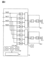
次いで図2には、半導体装置として機能する図1で図示したミキサー回路19のブロック図を示す。なお図2では、説明のため、アンプ回路20_1、20_2およびスピーカー21_1、21_2のブロック図を合わせて図示している。Fig. 2 shows a block diagram of the
図2では、ミキサー回路19の一例として、乗算回路30(一例として、乗算回路30_0乃至30_7を図示)、加算回路31(一例として加算回路31_1、31_2を図示)、信号生成部32および電源制御スイッチ33を有する構成を図示している。信号生成部32は、インターフェース34、制御回路35およびデジタルアナログ変換回路36を有する。2 illustrates, as an example of the
アンプ回路20_1、20_2は、比較回路51_1、比較回路51_2、スピーカー駆動回路52_1およびスピーカー駆動回路52_2を有する。比較回路51_1、比較回路51_2には、ミキサー回路19から出力される信号と、三角波生成回路53から出力される三角波と、が入力される。スピーカー駆動回路52_1およびスピーカー駆動回路52_2は、ミキサー回路19から出力される信号と三角波との比較結果に応じて、スピーカー21_1、21_2を制御するための信号を出力する機能を有する。The amplifier circuits 20_1 and 20_2 each have a comparison circuit 51_1, a comparison circuit 51_2, a speaker driving circuit 52_1, and a speaker driving circuit 52_2. The comparison circuit 51_1 and the comparison circuit 51_2 receive a signal output from the
乗算回路30は、入力される信号数に応じて乗算回路30_0乃至30_7のように複数設けられる。例えば、図1で説明したデジタルアナログ変換回路18を介してデジタルエフェクター15より出力されるアナログ音声データを信号WINとすると、図2では信号WINとして信号WIN[0]乃至WIN[3]が入力される。 A plurality of
また乗算回路30_0乃至30_7には、信号生成部32から信号CTRおよび信号WWが入力される。信号CTRは、乗算回路30_0乃至30_7が有するアナログ電位保持回路が有するトランジスタのオンまたはオフを制御するための信号である。信号WWは、乗算回路30_0乃至30_7が有するアナログ電位保持回路で保持する電位を与えるための信号である。 The multiplication circuits 30_0 to 30_7 also receive a signal CTR and a signal W_W from the signal generating unit 32. The signal CTR is a signal for controlling the on/off state of a transistor included in an analog potential holding circuit included in the multiplication circuits 30_0 to 30_7. The signal W_W is a signal for providing a potential to be held in the analog potential holding circuit included in the multiplication circuits 30_0 to 30_7.
信号生成部32が有するインターフェース34は、外部からデジタル信号を入力するためのインターフェースとして機能する。インターフェース34は、一例として、I2C(Inter Integrated Circuit)インターフェースを用いればよい。 The
制御回路35は、インターフェース34で受信する信号に応じて、デジタルアナログ変換回路36を制御するための信号、および信号CTRを生成する機能を有する。The
デジタルアナログ変換回路36は、制御回路35から出力されるデジタル信号に応じて、アナログ電位を出力するための信号である信号WWを生成するための回路である。デジタルアナログ変換回路36としては、一例として、ビットに応じた重みづけを行うキャパシタの充放電を行うことで、デジタル-アナログ変換を行う回路構成とすればよい。 The digital-
電源制御スイッチ33は、乗算回路30_0乃至30_7が有するアナログ電位保持回路の制御に応じて、信号生成部32が有する各回路への電源電圧の供給を制御する機能を有する回路である。例えば、前述のアナログ電位保持回路に信号WWを保持させた状態として、インターフェース34および制御回路35への電源電圧の供給を停止して、ミキサー回路19における消費電力の低減を図ることができる。 The power
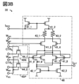
図3A、図3Bは、図2に図示する乗算回路30_0乃至30_7に適用可能な乗算回路30の構成例を説明するためのブロック図および回路図である。3A and 3B are a block diagram and a circuit diagram for explaining a configuration example of the
図3Aには、乗算回路として機能する回路のブロック図を図示している。図3Aに図示する乗算回路30は、差動信号で動作するギルバート回路として機能する回路に加え、信号WWのアナログ電位を信号CTRの制御に応じて保持することができるアナログ電位保持回路45N、45Pを有する。なおギルバート回路とは、2つの入力信号の乗算を行うことができる回路である。 Fig. 3A shows a block diagram of a circuit that functions as a multiplication circuit. The
図3Aに図示する乗算回路30のブロックに与えられる信号WWPおよび信号WWNは、信号WWに相当し、差動対となるトランジスタに与えられる信号である。信号WINPおよび信号WINNは、信号WINに相当し、差動対となるトランジスタに与えられる信号である。信号CTRNおよび信号CTRPは、信号CTRの信号に相当し、同じ論理の信号である。バイアス電流IBIASは、定電流を流すためのトランジスタに与える電流である。バックゲート電圧VBGは、アナログ電位保持回路45N、45Pが有するトランジスタのバックゲートに与える電圧である。信号IOUTは、信号WWと信号WINとの積に応じた電流である。 Signals W WP and W WN given to the block of the
図3Bは、図3Aに図示する乗算回路30のブロック図に適用可能な回路図である。乗算回路30は、トランジスタ41_1、トランジスタ41_2、トランジスタ41_3、トランジスタ41_4、トランジスタ41_5、トランジスタ41_6、トランジスタ41_7、トランジスタ41_8、トランジスタ42_1、トランジスタ42_2、抵抗43_1、および抵抗43_2で構成されるギルバート回路46と、ギルバート回路が有するトランジスタのゲートに接続されたトランジスタ44_1、およびトランジスタ44_2を有するアナログ電位保持回路45N、45Pを有する。なお図3Bに図示する各トランジスタのゲートには、図3Aで説明した各信号および電圧が与えられる。Fig. 3B is a circuit diagram applicable to the block diagram of the
図3Bにおいて、トランジスタ41_1、トランジスタ41_2、トランジスタ41_3、トランジスタ41_4、トランジスタ41_5、トランジスタ41_6、トランジスタ41_7、トランジスタ41_8は、チャネル形成領域がシリコンを有するトランジスタ(Siトランジスタ)で、pチャネル型のSiトランジスタである。トランジスタ42_1、トランジスタ42_2は、nチャネル型のSiトランジスタである。Siトランジスタは、CMOSテクノロジーで作製することができる。3B, transistors 41_1, 41_2, 41_3, 41_4, 41_5, 41_6, 41_7, and 41_8 are p-channel Si transistors having silicon in their channel formation regions (Si transistors). Transistors 42_1 and 42_2 are n-channel Si transistors. Si transistors can be manufactured by CMOS technology.
トランジスタ44_1、およびトランジスタ44_2は、チャネル形成領域が酸化物半導体を有するトランジスタ(以下、OSトランジスタという)で構成されることが好ましい。本発明の一態様の構成では、OSトランジスタをアナログ電位保持回路45N、45Pが有するトランジスタに用いる構成とすることで、オフ時にソースとドレイン間を流れるリーク電流(以下、オフ電流)が極めて低いことを利用して、信号WWのアナログ電位を信号CTRの制御に応じてアナログ電位保持回路45N、45Pに保持させることができる。 The transistors 44_1 and 44_2 are preferably transistors whose channel formation regions include an oxide semiconductor (hereinafter referred to as OS transistors). In one embodiment of the present invention, by using OS transistors as transistors included in the analog
信号WWによるアナログ電位の更新の頻度を低減することができ、信号WWを出力する信号生成部32の間欠的な動作を行わせることができる。電源制御スイッチ33は、アナログ電位保持回路が保持するアナログ電位を更新しない期間において信号生成部32の制御回路35への電源電圧の供給を停止する機能を有する。そのため、電源制御スイッチ33による信号生成部32の電源電圧の供給の停止による、ミキサー回路19の低消費電力化を図ることができる。 This reduces the frequency of updating the analog potential by the signal W W , and enables intermittent operation of the signal generating unit 32 that outputs the signal W W. The power
加えてOSトランジスタを用いたアナログ電位保持回路45N、45Pでは、電荷を充電又は放電することによってアナログ電圧の書き換えおよび読み出しが可能となるため、実質的に無制限回のアナログ電圧の取得および読み出しが可能である。OSトランジスタを用いたアナログ電位保持回路45N、45Pは、磁気メモリあるいは抵抗変化型メモリなどのように原子レベルでの構造変化を伴わないため、書き換え耐性に優れている。またOSトランジスタを用いたアナログ電位保持回路45N、45Pは、フラッシュメモリのように繰り返し書き換え動作でも電子捕獲中心の増加による不安定性が認められない。In addition, the analog
またOSトランジスタを用いたアナログ電位保持回路45N、45Pは、Siトランジスタを用いた回路上などに自由に配置可能であるため、複数のアナログ電位保持回路45N、45Pを備える構成した場合であっても、Siトランジスタで構成されるギルバート回路46上に集積化を容易に行うことができる。またOSトランジスタは、Siトランジスタと同様の製造装置を用いて作製することが可能であるため、低コストで作製可能である。Furthermore, since the analog
またOSトランジスタは、ゲート電極、ソース電極およびドレイン電極に加えて、バックゲート電極を含むと、4端子の半導体素子とすることができる。ゲート電極またはバックゲート電極に与える電圧に応じて、ソースとドレインとの間を流れる信号の入出力が独立制御可能な電気回路網で構成することができる。そのため、LSIと同一思考で回路設計を行うことができる。加えてOSトランジスタは、高温環境下において、Siトランジスタよりも優れた電気特性を有する。具体的には、125℃以上150℃以下といった高温下においてもオン電流とオフ電流の比が大きいため、良好なスイッチング動作を行うことができる。Furthermore, if an OS transistor includes a back gate electrode in addition to a gate electrode, a source electrode, and a drain electrode, it can be a four-terminal semiconductor element. It can be configured as an electric circuit network that can independently control the input and output of signals flowing between the source and drain according to the voltage applied to the gate electrode or the back gate electrode. Therefore, the circuit can be designed with the same concept as that of an LSI. In addition, an OS transistor has better electric characteristics than a Si transistor in a high-temperature environment. Specifically, since the ratio of the on current to the off current is large even at a high temperature of 125° C. or higher and 150° C. or lower, it can perform a good switching operation.
図4A、図4Bでは、図3A、図3Bで説明したアナログ電位保持回路45N、45Pに適用可能なアナログ電位保持回路45の動作を説明するためのブロック図および回路図を示す。なおアナログ電位保持回路45N、45Pは、差動信号として与えるアナログ電位を保持する回路であり、同じ回路構成を有する。そのため、アナログ電位保持回路45N、45Pの回路構成を説明する場合、アナログ電位保持回路45という場合がある。4A and 4B show a block diagram and a circuit diagram for explaining the operation of an analog
図4Aでは、上記図2、図3A、図3Bで説明した制御回路35、デジタルアナログ変換回路36、の他、乗算回路30として乗算回路30_0-30_7、アナログ電位保持回路45としてアナログ電位保持回路45_0-45_15を図示している。アナログ電位保持回路45_0-45_15は、例えば、アナログ電位保持回路45_0、45_1が、図3A、図3Bで説明したアナログ電位保持回路45N、45Pに対応する。また図4Aでは、上記図2、図3A、図3Bで説明した信号WWとして、信号WW[0]-信号WW[15]、信号CTRとして信号CTR[0]-CTR[15]、制御回路35からデジタルアナログ変換回路36に出力されるデジタルデータとして信号DATAを図示している。なお信号WW[0]-信号WW[15]の一対の信号は、図3A、図3Bで説明した信号WWPおよび信号WWNに対応する。また、信号CTR[0]-CTR[15]の一対の信号は、図3A、図3Bで説明した信号CTRNおよび信号CTRPに対応する。 4A illustrates the
図4Aに図示するように制御回路35は、信号DATAをデジタルアナログ変換回路36に出力する。デジタルアナログ変換回路36は、信号DATAに応じて、アナログ値の信号WW[0]-信号WW[15]を乗算回路30_0-30_7が有するアナログ電位保持回路45_0-45_15のそれぞれに出力する。また、制御回路35は、アナログ電位保持回路45_0-45_15が有するトランジスタのそれぞれにオンまたはオフを制御するための信号CTR[0]-CTR[15]を出力する。 4A, the
図4Bは、図4Aのアナログ電位保持回路45_0-45_15に適用可能な、アナログ電位保持回路45の回路構成を図示している。なお図4Bでは、説明のため、図4Aで説明した信号WW[0]-信号WW[15]を信号WW、信号CTR[0]-CTR[15]を信号CTRとして説明する。 Fig. 4B illustrates a circuit configuration of an analog
アナログ電位保持回路45は、OSトランジスタであるトランジスタ44を有する。トランジスタ44のソースまたはドレインの一方から信号WWが与えられる。信号WWに基づく電位は、トランジスタ44のソースまたはドレインの他方と、トランジスタ41のゲートと、が接続されたノードFNに保持される。トランジスタ41は、ギルバート回路46が有するSiトランジスタに相当する。ノードFNは、電荷を保持するためのキャパシタ47を有することが好ましい。トランジスタ44のゲートには、トランジスタ44のオンまたはオフを制御するための信号CTRが与えられる。トランジスタ44のバックゲートには、トランジスタ44のしきい値電圧を制御するためのバックゲート電圧VBGが印加される。 The analog
図5は、上記図2で説明した加算回路31の構成例を説明するための回路図である。図5では、加算回路31に入力される信号IOUTとして、信号IOUT_0-IOUT_3、オペアンプ61、抵抗62、加算回路31から出力される信号VOUTを図示している。VCOMは、基準電位である。一例として、図5に示す加算回路の構成とすることで電流を足し合わせた値に応じた電圧値の信号VOUTが得られる。 Fig. 5 is a circuit diagram for explaining a configuration example of the
図6は、上記図2で説明したデジタルアナログ変換回路36の構成例を説明するための回路図である。図6では、スイッチ71_1、71_2、キャパシタ72_1-72_10、切替スイッチ73_1-73_8およびオペアンプ74を図示している。なお図6では一例として8ビットの分解能を有するデジタルアナログ変換回路36を示す。キャパシタ72_1-72_10の容量比は、1:1:2:4:8:(8/7):1:2:4:8とする。8ビットのデジタル信号である信号DATAは、切替スイッチ73_1-73_8の切り替えを制御する信号となる。スイッチ71_1、71_2は、信号SRESによってオンまたはオフが制御される。切替スイッチ73_1-73_8は、電位VDDを与える配線と、電位VSS(<VDD)を与える配線と、の接続を切り替える。例えば、信号DATAがLレベルで電位VSSを与える配線に接続し、Hレベルで電位VDDを与える配線に切り替える構成とする。オペアンプ74は、アナログ値の信号AOUT(=信号WW)を出力することができる。 FIG. 6 is a circuit diagram for explaining a configuration example of the digital-
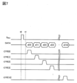
図7は、図5Bおよび図6で説明した回路における各信号の動作を説明するためのタイミングチャートを示す。図7では、信号DATAとして信号d[0]-d[15]を図示している。Fig. 7 is a timing chart for explaining the operation of each signal in the circuits explained in Fig. 5B and Fig. 6. In Fig. 7, signals d[0]-d[15] are illustrated as the signal DATA.
図7に図示するタイミングチャートでは、時刻t0でデジタルアナログ変換回路36の初期化を行う。初期化は、信号SRESをHレベルとしてスイッチ71_1、71_2をオンにすることで行われる。 7, the digital-
次いで時刻t1では、信号DATAとして信号d[0]をデジタルアナログ変換回路36に与える。デジタルアナログ変換回路36は、信号d[0]に応じたアナログ値の信号AOUT(=信号WW)を出力する。信号AOUTは、信号CTR[0]をHレベルとすることで、乗算回路30_0が有するアナログ電位保持回路45_0に書き込むことができる。その後、信号CTR[0]をLレベルとすることで、アナログ電位保持回路45_0には信号AOUTに応じた電位を保持し続けることができる。 Next, at time t1, the signal d[0] is provided to the digital-
以降、信号DATAとして信号d[1]-d[15]をデジタルアナログ変換回路36に与え、信号DATAに応じたアナログ値の信号AOUTをアナログ電位保持回路45に順次書き込むことができる。そのため、複数のチャンネルのゲインを1個のデジタルアナログ変換回路36で制御することができる。Thereafter, signals d[1]-d[15] are provided as signal DATA to the digital-
以上説明した本発明の一態様の半導体装置は、回路面積の増加を抑制することができる。または、消費電力の増加を抑制することができる。The above-described semiconductor device according to one embodiment of the present invention can suppress an increase in the circuit area or an increase in power consumption.
(実施の形態2)
本実施の形態では、上記実施の形態で説明した半導体装置の構成に適用可能なトランジスタの構成、具体的には異なる電気特性を有するトランジスタを積層して設ける構成について説明する。特に本実施の形態では、半導体装置を構成するミキサー回路が有する各トランジスタの構成について説明する。当該構成とすることで、半導体装置の設計自由度を高めることができる。また、異なる電気特性を有するトランジスタを積層して設けることで、半導体装置の集積度を高めることができる。(Embodiment 2)
In this embodiment, a transistor configuration applicable to the configuration of the semiconductor device described in the above embodiment, specifically, a configuration in which transistors having different electrical characteristics are stacked, will be described. In particular, in this embodiment, the configuration of each transistor included in a mixer circuit constituting the semiconductor device will be described. By using this configuration, it is possible to increase the degree of freedom in designing the semiconductor device. In addition, by stacking transistors having different electrical characteristics, it is possible to increase the integration degree of the semiconductor device.
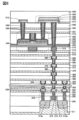
図8に示す半導体装置は、トランジスタ300と、トランジスタ500と、容量素子600と、を有している。図10Aはトランジスタ500のチャネル長方向の断面図であり、図10Bはトランジスタ500のチャネル幅方向の断面図であり、図10Cはトランジスタ300のチャネル幅方向の断面図である。8 includes a
トランジスタ500は、チャネル形成領域に金属酸化物を有するトランジスタ(OSトランジスタ)である。トランジスタ500は、オフ電流が小さいため、これを半導体装置が有するOSトランジスタに用いることにより、長期にわたり書き込んだデータ電圧あるいは電荷を保持することが可能である。つまり、リフレッシュ動作の頻度が少ない、あるいは、リフレッシュ動作を必要としないため、半導体装置の消費電力を低減することができる。The
本実施の形態で説明する半導体装置は、図8に示すようにトランジスタ300、トランジスタ500、容量素子600を有する。トランジスタ500はトランジスタ300の上方に設けられ、容量素子600はトランジスタ300、及びトランジスタ500の上方に設けられている。8, the semiconductor device described in this embodiment includes a
トランジスタ300は、基板311上に設けられ、導電体316、絶縁体315、基板311の一部からなる半導体領域313、ソース領域又はドレイン領域として機能する低抵抗領域314a、及び低抵抗領域314bを有する。なお、トランジスタ300は、例えば、上記実施の形態におけるギルバート回路46が有するトランジスタ等に適用することができる。The
トランジスタ300は、図10Cに示すように、半導体領域313の上面及びチャネル幅方向の側面が絶縁体315を介して導電体316に覆われている。このように、トランジスタ300をFin型とすることにより、実効上のチャネル幅が増大することによりトランジスタ300のオン特性を向上させることができる。また、ゲート電極の電界の寄与を高くすることができるため、トランジスタ300のオフ特性を向上させることができる。10C , the upper surface and the side surface in the channel width direction of the
なお、トランジスタ300は、pチャネル型、あるいはnチャネル型のいずれでもよい。The
半導体領域313のチャネルが形成される領域、その近傍の領域、ソース領域、又はドレイン領域となる低抵抗領域314a、及び低抵抗領域314bなどにおいて、シリコン系半導体などの半導体を含むことが好ましく、単結晶シリコンを含むことが好ましい。又は、Ge(ゲルマニウム)、SiGe(シリコンゲルマニウム)、GaAs(ガリウムヒ素)、GaAlAs(ガリウムアルミニウムヒ素)などを有する材料で形成してもよい。結晶格子に応力を与え、格子間隔を変化させることで有効質量を制御したシリコンを用いた構成としてもよい。又はGaAsとGaAlAs等を用いることで、トランジスタ300をHEMT(High Electron Mobility Transistor)としてもよい。The region where the channel of the
低抵抗領域314a、及び低抵抗領域314bは、半導体領域313に適用される半導体材料に加え、ヒ素、リンなどのn型の導電性を付与する元素、又はホウ素などのp型の導電性を付与する元素を含む。The
ゲート電極として機能する導電体316は、ヒ素、リンなどのn型の導電性を付与する元素、もしくはホウ素などのp型の導電性を付与する元素を含むシリコンなどの半導体材料、金属材料、合金材料、又は金属酸化物材料などの導電性材料を用いることができる。The
なお、導電体の材料によって仕事関数が決まるため、当該導電体の材料を選択することで、トランジスタのしきい値電圧を調整することができる。具体的には、導電体に窒化チタンや窒化タンタルなどの材料を用いることが好ましい。さらに導電性と埋め込み性を両立するために導電体にタングステンやアルミニウムなどの金属材料を積層として用いることが好ましく、特にタングステンを用いることが耐熱性の点で好ましい。Since the work function is determined by the material of the conductor, the threshold voltage of the transistor can be adjusted by selecting the material of the conductor. Specifically, it is preferable to use a material such as titanium nitride or tantalum nitride for the conductor. Furthermore, in order to achieve both electrical conductivity and embeddability, it is preferable to use a metal material such as tungsten or aluminum as the conductor in a laminated state, and in particular, it is preferable to use tungsten in terms of heat resistance.
なお、図8に示すトランジスタ300は一例であり、その構造に限定されず、回路構成や駆動方法に応じて適切なトランジスタを用いればよい。例えば、半導体装置をOSトランジスタのみの単極性回路(nチャネル型トランジスタのみ、など同極性のトランジスタで構成される回路を意味する)とする場合、図9に示すとおり、トランジスタ300の構成を、酸化物半導体を用いているトランジスタ500と同様の構成にすればよい。なお、トランジスタ500の詳細については後述する。8 is an example, and is not limited to the structure, and an appropriate transistor may be used depending on the circuit configuration and driving method. For example, when the semiconductor device is a unipolar circuit including only OS transistors (meaning a circuit including transistors of the same polarity, such as only n-channel transistors), the structure of the
トランジスタ300を覆って、絶縁体320、絶縁体322、絶縁体324、及び絶縁体326が順に積層して設けられている。An
絶縁体320、絶縁体322、絶縁体324、及び絶縁体326として、例えば、酸化シリコン、酸化窒化シリコン、窒化酸化シリコン、窒化シリコン、酸化アルミニウム、酸化窒化アルミニウム、窒化酸化アルミニウム、窒化アルミニウムなどを用いればよい。As the
なお、本明細書中において、酸化窒化シリコンとは、その組成として窒素よりも酸素の含有量が多い材料を指し、窒化酸化シリコンとは、その組成として、酸素よりも窒素の含有量が多い材料を示す。また、本明細書中において、酸化窒化アルミニウムとは、その組成として窒素よりも酸素の含有量が多い材料を指し、窒化酸化アルミニウムとは、その組成として、酸素よりも窒素の含有量が多い材料を示す。In this specification, silicon oxynitride refers to a material that contains more oxygen than nitrogen, silicon nitride oxide refers to a material that contains more nitrogen than oxygen, aluminum oxynitride refers to a material that contains more oxygen than nitrogen, and aluminum nitride oxide refers to a material that contains more nitrogen than oxygen.
絶縁体322は、その下方に設けられるトランジスタ300などによって生じる段差を平坦化する平坦化膜としての機能を有していてもよい。例えば、絶縁体322の上面は、平坦性を高めるために化学機械研磨(CMP)法等を用いた平坦化処理により平坦化されていてもよい。The
また、絶縁体324には、基板311、又はトランジスタ300などから、トランジスタ500が設けられる領域に、水素や不純物が拡散しないようなバリア性を有する膜を用いることが好ましい。The
水素に対するバリア性を有する膜の一例として、例えば、CVD法で形成した窒化シリコンを用いることができる。ここで、トランジスタ500等の酸化物半導体を有する半導体素子に、水素が拡散することで、当該半導体素子の特性が低下する場合がある。したがって、トランジスタ500と、トランジスタ300との間に、水素の拡散を抑制する膜を用いることが好ましい。水素の拡散を抑制する膜とは、具体的には、水素の脱離量が少ない膜とする。As an example of a film having a barrier property against hydrogen, for example, silicon nitride formed by a CVD method can be used. Here, when hydrogen diffuses into a semiconductor element having an oxide semiconductor such as the
水素の脱離量は、例えば、昇温脱離ガス分析法(TDS)などを用いて分析することができる。例えば、絶縁体324の水素の脱離量は、TDS分析において、膜の表面温度が50℃から500℃の範囲において、水素原子に換算した脱離量が、絶縁体324の面積当たりに換算して、10×1015atoms/cm2以下、好ましくは5×1015atoms/cm2以下であればよい。 The amount of desorption of hydrogen can be analyzed, for example, by using thermal desorption spectroscopy (TDS) etc. For example, the amount of desorption of hydrogen from the
なお、絶縁体326は、絶縁体324よりも誘電率が低いことが好ましい。例えば、絶縁体326の比誘電率は4未満が好ましく、3未満がより好ましい。また例えば、絶縁体326の比誘電率は、絶縁体324の比誘電率の0.7倍以下が好ましく、0.6倍以下がより好ましい。誘電率が低い材料を層間膜とすることで、配線間に生じる寄生容量を低減することができる。Note that the
また、絶縁体320、絶縁体322、絶縁体324、及び絶縁体326には容量素子600、又はトランジスタ500と接続する導電体328、及び導電体330等が埋め込まれている。なお、導電体328、及び導電体330は、プラグ又は配線としての機能を有する。また、プラグ又は配線としての機能を有する導電体は、複数の構造をまとめて同一の符号を付与する場合がある。また、本明細書等において、配線と、配線と接続するプラグとが一体物であってもよい。すなわち、導電体の一部が配線として機能する場合、及び導電体の一部がプラグとして機能する場合もある。
各プラグ、及び配線(導電体328、導電体330等)の材料としては、金属材料、合金材料、金属窒化物材料、又は金属酸化物材料などの導電性材料を、単層又は積層して用いることができる。耐熱性と導電性を両立するタングステンやモリブデンなどの高融点材料を用いることが好ましく、特にタングステンを用いることが好ましい。又は、アルミニウムや銅などの低抵抗導電性材料で形成することが好ましい。低抵抗導電性材料を用いることで配線抵抗を低くすることができる。As the material for each plug and wiring (
絶縁体326、及び導電体330上に、配線層を設けてもよい。例えば、図8において、絶縁体350、絶縁体352、及び絶縁体354が順に積層して設けられている。また、絶縁体350、絶縁体352、及び絶縁体354には、導電体356が形成されている。導電体356は、トランジスタ300と接続するプラグ、又は配線としての機能を有する。なお導電体356は、導電体328、及び導電体330と同様の材料を用いて設けることができる。A wiring layer may be provided over the
なお、例えば、絶縁体350は、絶縁体324と同様に、水素に対するバリア性を有する絶縁体を用いることが好ましい。また、導電体356は、水素に対するバリア性を有する導電体を含むことが好ましい。特に、水素に対するバリア性を有する絶縁体350が有する開口部に、水素に対するバリア性を有する導電体が形成される。当該構成により、トランジスタ300とトランジスタ500とは、バリア層により分離することができ、トランジスタ300からトランジスタ500への水素の拡散を抑制することができる。Note that, for example, the
なお、水素に対するバリア性を有する導電体としては、例えば、窒化タンタル等を用いるとよい。また、窒化タンタルと導電性が高いタングステンを積層することで、配線としての導電性を保持したまま、トランジスタ300からの水素の拡散を抑制することができる。この場合、水素に対するバリア性を有する窒化タンタル層が、水素に対するバリア性を有する絶縁体350と接する構造であることが好ましい。Note that, for example, tantalum nitride or the like may be used as the conductor having a barrier property against hydrogen. By stacking tantalum nitride and tungsten having high conductivity, diffusion of hydrogen from the
絶縁体354、及び導電体356上に、配線層を設けてもよい。例えば、図8において、絶縁体360、絶縁体362、及び絶縁体364が順に積層して設けられている。また、絶縁体360、絶縁体362、及び絶縁体364には、導電体366が形成されている。導電体366は、プラグ又は配線としての機能を有する。なお導電体366は、導電体328、及び導電体330と同様の材料を用いて設けることができる。A wiring layer may be provided over the
なお、例えば、絶縁体360は、絶縁体324と同様に、水素に対するバリア性を有する絶縁体を用いることが好ましい。また、導電体366は、水素に対するバリア性を有する導電体を含むことが好ましい。特に、水素に対するバリア性を有する絶縁体360が有する開口部に、水素に対するバリア性を有する導電体が形成される。当該構成により、トランジスタ300とトランジスタ500とは、バリア層により分離することができ、トランジスタ300からトランジスタ500への水素の拡散を抑制することができる。Note that, for example, the
絶縁体364、及び導電体366上に、配線層を設けてもよい。例えば、図8において、絶縁体370、絶縁体372、及び絶縁体374が順に積層して設けられている。また、絶縁体370、絶縁体372、及び絶縁体374には、導電体376が形成されている。導電体376は、プラグ又は配線としての機能を有する。なお導電体376は、導電体328、及び導電体330と同様の材料を用いて設けることができる。A wiring layer may be provided over the
なお、例えば、絶縁体370は、絶縁体324と同様に、水素に対するバリア性を有する絶縁体を用いることが好ましい。また、導電体376は、水素に対するバリア性を有する導電体を含むことが好ましい。特に、水素に対するバリア性を有する絶縁体370が有する開口部に、水素に対するバリア性を有する導電体が形成される。当該構成により、トランジスタ300とトランジスタ500とは、バリア層により分離することができ、トランジスタ300からトランジスタ500への水素の拡散を抑制することができる。Note that, for example, the
絶縁体374、及び導電体376上に、配線層を設けてもよい。例えば、図8において、絶縁体380、絶縁体382、及び絶縁体384が順に積層して設けられている。また、絶縁体380、絶縁体382、及び絶縁体384には、導電体386が形成されている。導電体386は、プラグ又は配線としての機能を有する。なお導電体386は、導電体328、及び導電体330と同様の材料を用いて設けることができる。A wiring layer may be provided over the
なお、例えば、絶縁体380は、絶縁体324と同様に、水素に対するバリア性を有する絶縁体を用いることが好ましい。また、導電体386は、水素に対するバリア性を有する導電体を含むことが好ましい。特に、水素に対するバリア性を有する絶縁体380が有する開口部に、水素に対するバリア性を有する導電体が形成される。当該構成により、トランジスタ300とトランジスタ500とは、バリア層により分離することができ、トランジスタ300からトランジスタ500への水素の拡散を抑制することができる。Note that, for example, the
上記において、導電体356を含む配線層、導電体366を含む配線層、導電体376を含む配線層、及び導電体386を含む配線層、について説明したが、本実施の形態に係る半導体装置はこれに限られるものではない。導電体356を含む配線層と同様の配線層を3層以下にしてもよいし、導電体356を含む配線層と同様の配線層を5層以上にしてもよい。In the above, a wiring layer including the
絶縁体384上には絶縁体510、絶縁体512、絶縁体514、及び絶縁体516が、順に積層して設けられている。絶縁体510、絶縁体512、絶縁体514、及び絶縁体516のいずれかは、酸素や水素に対してバリア性のある物質を用いることが好ましい。An
例えば、絶縁体510、及び絶縁体514には、例えば、基板311、又はトランジスタ300を設ける領域などから、トランジスタ500を設ける領域に、水素や不純物が拡散しないようなバリア性を有する膜を用いることが好ましい。したがって、絶縁体324と同様の材料を用いることができる。For example, the
水素に対するバリア性を有する膜の一例として、CVD法で形成した窒化シリコンを用いることができる。ここで、トランジスタ500等の酸化物半導体を有する半導体素子に、水素が拡散することで、当該半導体素子の特性が低下する場合がある。したがって、トランジスタ500と、トランジスタ300との間に、水素の拡散を抑制する膜を用いることが好ましい。水素の拡散を抑制する膜とは、具体的には、水素の脱離量が少ない膜とする。As an example of a film having a barrier property against hydrogen, silicon nitride formed by a CVD method can be used. Here, when hydrogen diffuses into a semiconductor element having an oxide semiconductor such as the
また、水素に対するバリア性を有する膜として、例えば、絶縁体510、及び絶縁体514には、酸化アルミニウム、酸化ハフニウム、酸化タンタルなどの金属酸化物を用いることが好ましい。As a film having a barrier property against hydrogen, for example, the
特に、酸化アルミニウムは、酸素、及びトランジスタの電気特性の変動要因となる水素、水分などの不純物、の両方に対して膜を透過させない遮断効果が高い。したがって、酸化アルミニウムは、トランジスタの作製工程中及び作製後において、水素、水分などの不純物のトランジスタ500への混入を防止することができる。また、トランジスタ500を構成する酸化物からの酸素の放出を抑制することができる。そのため、トランジスタ500に対する保護膜として用いることに適している。In particular, aluminum oxide has a high blocking effect of preventing the film from permeating both oxygen and impurities such as hydrogen and moisture, which are factors that cause fluctuations in the electrical characteristics of a transistor. Therefore, aluminum oxide can prevent impurities such as hydrogen and moisture from entering the
また、例えば、絶縁体512、及び絶縁体516には、絶縁体320と同様の材料を用いることができる。また、これらの絶縁体に、比較的誘電率が低い材料を適用することで、配線間に生じる寄生容量を低減することができる。例えば、絶縁体512、及び絶縁体516として、酸化シリコン膜や酸化窒化シリコン膜などを用いることができる。For example, the
また、絶縁体510、絶縁体512、絶縁体514、及び絶縁体516には、導電体518、及びトランジスタ500を構成する導電体(例えば、導電体503)等が埋め込まれている。なお、導電体518は、容量素子600、又はトランジスタ300と接続するプラグ、又は配線としての機能を有する。導電体518は、導電体328、及び導電体330と同様の材料を用いて設けることができる。A
特に、絶縁体510、及び絶縁体514と接する領域の導電体518は、酸素、水素、及び水に対するバリア性を有する導電体であることが好ましい。当該構成により、トランジスタ300とトランジスタ500とは、酸素、水素、及び水に対するバリア性を有する層で、分離することができ、トランジスタ300からトランジスタ500への水素の拡散を抑制することができる。In particular, the
絶縁体516の上方には、トランジスタ500が設けられている。Above the
図10A、図10Bに示すように、トランジスタ500は、絶縁体514及び絶縁体516に埋め込まれるように配置された導電体503と、絶縁体516及び導電体503の上に配置された絶縁体520と、絶縁体520の上に配置された絶縁体522と、絶縁体522の上に配置された絶縁体524と、絶縁体524の上に配置された酸化物530aと、酸化物530aの上に配置された酸化物530bと、酸化物530b上に互いに離れて配置された導電体542a及び導電体542bと、導電体542a及び導電体542b上に配置され、導電体542aと導電体542bの間に重畳して開口が形成された絶縁体580と、開口の底面及び側面に配置された酸化物530cと、酸化物530cの形成面に配置された絶縁体550と、絶縁体550の形成面に配置された導電体560と、を有する。As shown in Figures 10A and 10B, the
また、図10A、図10Bに示すように、酸化物530a、酸化物530b、導電体542a、及び導電体542bと、絶縁体580との間に絶縁体544が配置されることが好ましい。また、図10A、図10Bに示すように、導電体560は、絶縁体550の内側に設けられた導電体560aと、導電体560aの内側に埋め込まれるように設けられた導電体560bと、を有することが好ましい。また、図10A、図10Bに示すように、絶縁体580、導電体560、絶縁体550及び酸化物530cの上に絶縁体574が配置されることが好ましい。10A and 10B, it is preferable that an
なお、以下において、酸化物530a、酸化物530b、及び酸化物530cをまとめて酸化物530という場合がある。In the following,
なお、トランジスタ500では、チャネルが形成される領域と、その近傍において、酸化物530a、酸化物530b、及び酸化物530cの3層を積層する構成について示しているが、本発明はこれに限られるものではない。例えば、酸化物530bの単層、酸化物530bと酸化物530aの2層構造、酸化物530bと酸化物530cの2層構造、又は4層以上の積層構造を設ける構成にしてもよい。また、トランジスタ500では、導電体560を2層の積層構造として示しているが、本発明はこれに限られるものではない。例えば、導電体560が、単層構造であってもよいし、3層以上の積層構造であってもよい。また、図8、図10Aに示すトランジスタ500は一例であり、その構造に限定されず、回路構成や駆動方法に応じて適切なトランジスタを用いればよい。In the
ここで、導電体560は、トランジスタのゲート電極として機能し、導電体542a及び導電体542bは、それぞれソース電極又はドレイン電極として機能する。上記のように、導電体560は、絶縁体580の開口、及び導電体542aと導電体542bに挟まれた領域に埋め込まれるように形成される。導電体560、導電体542a及び導電体542bの配置は、絶縁体580の開口に対して、自己整合的に選択される。つまり、トランジスタ500において、ゲート電極を、ソース電極とドレイン電極の間に、自己整合的に配置させることができる。よって、導電体560を位置合わせのマージンを設けることなく形成することができるので、トランジスタ500の占有面積の縮小を図ることができる。これにより、半導体装置の微細化、高集積化を図ることができる。Here, the
さらに、導電体560が、導電体542aと導電体542bの間の領域に自己整合的に形成されるので、導電体560は、導電体542a又は導電体542bと重畳する領域を有さない。これにより、導電体560と導電体542a及び導電体542bとの間に形成される寄生容量を低減することができる。よって、トランジスタ500のスイッチング速度を向上させ、高い周波数特性を有せしめることができる。Furthermore, since the
導電体560は、第1のゲート(トップゲートともいう)電極として機能する場合がある。また、導電体503は、第2のゲート(ボトムゲートともいう)電極として機能する場合がある。その場合、導電体503に印加する電位を、導電体560に印加する電位と、連動させず、独立して変化させることで、トランジスタ500のしきい値電圧を制御することができる。特に、導電体503に負の電位を印加することにより、トランジスタ500のしきい値電圧を0Vより大きくし、オフ電流を低減することが可能となる。したがって、導電体503に負の電位を印加したほうが、印加しない場合よりも、導電体560に印加する電位が0Vのときのドレイン電流を小さくすることができる。The
導電体503は、酸化物530、及び導電体560と、重なるように配置する。これにより、導電体560、及び導電体503に電位を印加した場合、導電体560から生じる電界と、導電体503から生じる電界と、がつながり、酸化物530に形成されるチャネル形成領域を覆うことができる。本明細書等において、第1のゲート電極、及び第2のゲート電極の電界によって、チャネル形成領域を電気的に取り囲むトランジスタの構造を、surrounded channel(S-channel)構造とよぶ。The
また、導電体503は、導電体518と同様の構成であり、絶縁体514及び絶縁体516の開口の内壁に接して導電体503aが形成され、さらに内側に導電体503bが形成されている。なお、トランジスタ500では、導電体503a及び導電体503bを積層する構成について示しているが、本発明はこれに限られるものではない。例えば、導電体503は、単層、又は3層以上の積層構造として設ける構成にしてもよい。The
ここで、導電体503aは、水素原子、水素分子、水分子、銅原子などの不純物の拡散を抑制する機能を有する(上記不純物が透過しにくい)導電性材料を用いることが好ましい。又は、酸素(例えば、酸素原子、酸素分子などの少なくとも一)の拡散を抑制する機能を有する(上記酸素が透過しにくい)導電性材料を用いることが好ましい。なお、本明細書において、不純物、又は酸素の拡散を抑制する機能とは、上記不純物、又は上記酸素のいずれか一又は、すべての拡散を抑制する機能とする。Here, the
例えば、導電体503aが酸素の拡散を抑制する機能を持つことにより、導電体503bが酸化して導電率が低下することを抑制することができる。For example, the
また、導電体503が配線の機能を兼ねる場合、導電体503bは、タングステン、銅、又はアルミニウムを主成分とする、導電性が高い導電性材料を用いることが好ましい。なお、導電体503bを単層で図示したが、積層構造としてもよく、例えば、チタンまたは窒化チタンと上記導電性材料との積層としてもよい。In addition, when the
絶縁体520、絶縁体522、および絶縁体524は、第2のゲート絶縁膜としての機能を有する。The
ここで、酸化物530と接する絶縁体524は、化学量論的組成を満たす酸素よりも多くの酸素を含む絶縁体を用いることが好ましい。つまり、絶縁体524には、過剰酸素領域が形成されていることが好ましい。このような過剰酸素を含む絶縁体を酸化物530に接して設けることにより、酸化物530中の酸素欠損を低減し、トランジスタ500の信頼性を向上させることができる。Here, the
過剰酸素領域を有する絶縁体として、具体的には、加熱により一部の酸素が脱離する酸化物材料を用いることが好ましい。加熱により酸素を脱離する酸化物とは、TDS(Thermal Desorption Spectroscopy)分析にて、酸素原子に換算しての酸素の脱離量が1.0×10¹⁸atoms/cm3以上、好ましくは1.0×1019atoms/cm3以上、さらに好ましくは2.0×1019atoms/cm3以上、又は3.0×1020atoms/cm3以上である酸化物膜である。なお、上記TDS分析時における膜の表面温度としては100℃以上700℃以下、又は100℃以上400℃以下の範囲が好ましい。 Specifically, it is preferable to use an oxide material from which part of oxygen is released by heating as an insulator having an excess oxygen region. The oxide from which oxygen is released by heating is an oxide film from which the amount of oxygen released, calculated as oxygen atoms, is 1.0×10 18 atoms/cm 3 or more, preferably 1.0×10 19 atoms/cm 3 or more, more preferably 2.0×10 19 atoms/cm 3 or more, or 3.0×10 20 atoms/cm 3 or more, in TDS (Thermal Desorption Spectroscopy) analysis. The surface temperature of the film during the TDS analysis is preferably in the range of 100° C. to 700° C., or 100° C. to 400° C.
また、絶縁体524が、過剰酸素領域を有する場合、絶縁体522は、酸素(例えば、酸素原子、酸素分子など)の拡散を抑制する機能を有する(上記酸素が透過しにくい)ことが好ましい。Furthermore, when the
絶縁体522が、酸素や不純物の拡散を抑制する機能を有することで、酸化物530が有する酸素は、絶縁体520側へ拡散することがなく、好ましい。また、導電体503が、絶縁体524や、酸化物530が有する酸素と反応することを抑制することができる。The
絶縁体522は、例えば、酸化アルミニウム、酸化ハフニウム、アルミニウム及びハフニウムを含む酸化物(ハフニウムアルミネート)、酸化タンタル、酸化ジルコニウム、チタン酸ジルコン酸鉛(PZT)、チタン酸ストロンチウム(SrTiO3)、又は(Ba,Sr)TiO3(BST)などのいわゆるhigh-k材料を含む絶縁体を単層又は積層で用いることが好ましい。トランジスタの微細化、及び高集積化が進むと、ゲート絶縁膜の薄膜化により、リーク電流などの問題が生じる場合がある。ゲート絶縁膜として機能する絶縁体にhigh-k材料を用いることで、物理膜厚を保ちながら、トランジスタ動作時のゲート電位の低減が可能となる。 The
特に、不純物、及び酸素などの拡散を抑制する機能を有する(上記酸素が透過しにくい)絶縁性材料であるアルミニウム、ハフニウムの一方又は双方の酸化物を含む絶縁体を用いるとよい。アルミニウム、ハフニウムの一方又は双方の酸化物を含む絶縁体として、酸化アルミニウム、酸化ハフニウム、アルミニウム及びハフニウムを含む酸化物(ハフニウムアルミネート)などを用いることが好ましい。このような材料を用いて絶縁体522を形成した場合、絶縁体522は、酸化物530からの酸素の放出や、トランジスタ500の周辺部から酸化物530への水素等の不純物の混入を抑制する層として機能する。In particular, it is preferable to use an insulator containing an oxide of one or both of aluminum and hafnium, which are insulating materials having a function of suppressing the diffusion of impurities and oxygen (the oxygen is unlikely to permeate through them). As an insulator containing an oxide of one or both of aluminum and hafnium, it is preferable to use aluminum oxide, hafnium oxide, an oxide containing aluminum and hafnium (hafnium aluminate), or the like. When the
又は、これらの絶縁体に、例えば、酸化アルミニウム、酸化ビスマス、酸化ゲルマニウム、酸化ニオブ、酸化シリコン、酸化チタン、酸化タングステン、酸化イットリウム、酸化ジルコニウムを添加してもよい。又はこれらの絶縁体を窒化処理してもよい。上記の絶縁体に酸化シリコン、酸化窒化シリコン又は窒化シリコンを積層して用いてもよい。Alternatively, for example, aluminum oxide, bismuth oxide, germanium oxide, niobium oxide, silicon oxide, titanium oxide, tungsten oxide, yttrium oxide, or zirconium oxide may be added to these insulators. Alternatively, these insulators may be nitrided. Silicon oxide, silicon oxynitride, or silicon nitride may be stacked on the above insulators.
また、絶縁体520は、熱的に安定していることが好ましい。例えば、酸化シリコン及び酸化窒化シリコンは、熱的に安定であるため、好適である。また、high-k材料の絶縁体を酸化シリコン、または酸化窒化シリコンと組み合わせることで、熱的に安定かつ比誘電率の高い積層構造の絶縁体520を得ることができる。Moreover, it is preferable that the
なお、図10A、図10Bのトランジスタ500では、3層の積層構造からなる第2のゲート絶縁膜として、絶縁体520、絶縁体522、及び絶縁体524が図示されているが、第2のゲート絶縁膜は、単層、2層、又は4層以上の積層構造を有していてもよい。その場合、同じ材料からなる積層構造に限定されず、異なる材料からなる積層構造でもよい。10A and 10B, the
トランジスタ500は、チャネル形成領域を含む酸化物530に、酸化物半導体として機能する金属酸化物を用いることが好ましい。例えば、酸化物530として、In-M-Zn酸化物(元素Mは、アルミニウム、ガリウム、イットリウム、銅、バナジウム、ベリリウム、ホウ素、チタン、鉄、ニッケル、ゲルマニウム、ジルコニウム、モリブデン、ランタン、セリウム、ネオジム、ハフニウム、タンタル、タングステン、又はマグネシウムなどから選ばれた一種、又は複数種)等の金属酸化物を用いるとよい。また、酸化物530として、In-Ga酸化物、In-Zn酸化物を用いてもよい。In the
酸化物530においてチャネル形成領域として機能する金属酸化物は、バンドギャップが2eV以上、好ましくは2.5eV以上のものを用いることが好ましい。このように、バンドギャップの大きい金属酸化物を用いることで、トランジスタのオフ電流を低減することができる。A metal oxide that functions as a channel formation region in the
酸化物530は、酸化物530b下に酸化物530aを有することで、酸化物530aよりも下方に形成された構造物から、酸化物530bへの不純物の拡散を抑制することができる。また、酸化物530b上に酸化物530cを有することで、酸化物530cよりも上方に形成された構造物から、酸化物530bへの不純物の拡散を抑制することができる。The
なお、酸化物530は、各金属原子の原子数比が異なる複数の酸化物層の積層構造を有することが好ましい。具体的には、酸化物530aに用いる金属酸化物において、構成元素中の元素Mの原子数比が、酸化物530bに用いる金属酸化物における、構成元素中の元素Mの原子数比より、大きいことが好ましい。また、酸化物530aに用いる金属酸化物において、Inに対する元素Mの原子数比が、酸化物530bに用いる金属酸化物における、Inに対する元素Mの原子数比より大きいことが好ましい。また、酸化物530bに用いる金属酸化物において、元素Mに対するInの原子数比が、酸化物530aに用いる金属酸化物における、元素Mに対するInの原子数比より大きいことが好ましい。また、酸化物530cは、酸化物530a又は酸化物530bに用いることができる金属酸化物を、用いることができる。The
また、酸化物530a及び酸化物530cの伝導帯下端のエネルギーが、酸化物530bの伝導帯下端のエネルギーより高くなることが好ましい。また、言い換えると、酸化物530a及び酸化物530cの電子親和力が、酸化物530bの電子親和力より小さいことが好ましい。In addition, it is preferable that the energy of the conduction band minimum of the
ここで、酸化物530a、酸化物530b、及び酸化物530cの接合部において、伝導帯下端のエネルギー準位はなだらかに変化する。換言すると、酸化物530a、酸化物530b、及び酸化物530cの接合部における伝導帯下端のエネルギー準位は、連続的に変化又は連続接合するともいうことができる。このようにするためには、酸化物530aと酸化物530bとの界面、及び酸化物530bと酸化物530cとの界面において形成される混合層の欠陥準位密度を低くするとよい。Here, the energy level of the conduction band minimum changes gradually at the junction between the
具体的には、酸化物530aと酸化物530b、酸化物530bと酸化物530cが、酸素以外に共通の元素を有する(主成分とする)ことで、欠陥準位密度が低い混合層を形成することができる。例えば、酸化物530bがIn-Ga-Zn酸化物の場合、酸化物530a及び酸化物530cとして、In-Ga-Zn酸化物、Ga-Zn酸化物、酸化ガリウムなどを用いるとよい。Specifically, the
このとき、キャリアの主たる経路は酸化物530bとなる。酸化物530a、酸化物530cを上述の構成とすることで、酸化物530aと酸化物530bとの界面、及び酸化物530bと酸化物530cとの界面における欠陥準位密度を低くすることができる。そのため、界面散乱によるキャリア伝導への影響が小さくなり、トランジスタ500は高いオン電流を得られる。At this time, the main carrier path is the
酸化物530b上には、ソース電極、及びドレイン電極として機能する導電体542a、及び導電体542bが設けられる。導電体542a、及び導電体542bとしては、アルミニウム、クロム、銅、銀、金、白金、タンタル、ニッケル、チタン、モリブデン、タングステン、ハフニウム、バナジウム、ニオブ、マンガン、マグネシウム、ジルコニウム、ベリリウム、インジウム、ルテニウム、イリジウム、ストロンチウム、ランタンから選ばれた金属元素、又は上述した金属元素を成分とする合金か、上述した金属元素を組み合わせた合金等を用いることが好ましい。例えば、窒化タンタル、窒化チタン、タングステン、チタンとアルミニウムを含む窒化物、タンタルとアルミニウムを含む窒化物、酸化ルテニウム、窒化ルテニウム、ストロンチウムとルテニウムを含む酸化物、ランタンとニッケルを含む酸化物などを用いることが好ましい。また、窒化タンタル、窒化チタン、チタンとアルミニウムを含む窒化物、タンタルとアルミニウムを含む窒化物、酸化ルテニウム、窒化ルテニウム、ストロンチウムとルテニウムを含む酸化物、ランタンとニッケルを含む酸化物は、酸化しにくい導電性材料、又は、酸素を吸収しても導電性を維持する材料であるため、好ましい。更に、窒化タンタルなどの金属窒化物膜は、水素又は酸素に対するバリア性があるため好ましい。
また、図10では、導電体542a、及び導電体542bを単層構造として示したが、2層以上の積層構造としてもよい。例えば、窒化タンタル膜とタングステン膜を積層するとよい。また、チタン膜とアルミニウム膜を積層してもよい。また、タングステン膜上にアルミニウム膜を積層する二層構造、銅-マグネシウム-アルミニウム合金膜上に銅膜を積層する二層構造、チタン膜上に銅膜を積層する二層構造、タングステン膜上に銅膜を積層する二層構造としてもよい。10, the
また、チタン膜又は窒化チタン膜と、そのチタン膜又は窒化チタン膜上に重ねてアルミニウム膜又は銅膜を積層し、さらにその上にチタン膜又は窒化チタン膜を形成する三層構造、モリブデン膜又は窒化モリブデン膜と、そのモリブデン膜又は窒化モリブデン膜上に重ねてアルミニウム膜又は銅膜を積層し、さらにその上にモリブデン膜又は窒化モリブデン膜を形成する三層構造等がある。なお、酸化インジウム、酸化錫又は酸化亜鉛を含む透明導電材料を用いてもよい。In addition, there are three-layer structures in which a titanium film or titanium nitride film is laminated on the titanium film or titanium nitride film, an aluminum film or copper film is laminated on the titanium film or titanium nitride film, and a titanium film or titanium nitride film is further formed thereon, and a three-layer structure in which a molybdenum film or molybdenum nitride film is laminated on the molybdenum film or molybdenum nitride film, an aluminum film or copper film is laminated on the molybdenum film or molybdenum nitride film, and a molybdenum film or molybdenum nitride film is further formed thereon, etc. Note that a transparent conductive material containing indium oxide, tin oxide, or zinc oxide may be used.
また、図10Aに示すように、酸化物530の、導電体542a(導電体542b)との界面とその近傍には、低抵抗領域として、領域543a、及び領域543bが形成される場合がある。このとき、領域543aはソース領域又はドレイン領域の一方として機能し、領域543bはソース領域又はドレイン領域の他方として機能する。また、領域543aと領域543bに挟まれる領域にチャネル形成領域が形成される。10A ,
酸化物530と接するように上記導電体542a(導電体542b)を設けることで、領域543a(領域543b)の酸素濃度が低減する場合がある。また、領域543a(領域543b)に導電体542a(導電体542b)に含まれる金属と、酸化物530の成分とを含む金属化合物層が形成される場合がある。このような場合、領域543a(領域543b)のキャリア密度が増加し、領域543a(領域543b)は、低抵抗領域となる。By providing the
絶縁体544は、導電体542a、及び導電体542bを覆うように設けられ、導電体542a、及び導電体542bの酸化を抑制する。このとき、絶縁体544は、酸化物530の側面を覆い、絶縁体524と接するように設けられてもよい。The
絶縁体544として、ハフニウム、アルミニウム、ガリウム、イットリウム、ジルコニウム、タングステン、チタン、タンタル、ニッケル、ゲルマニウム、ネオジム、ランタン又は、マグネシウムなどから選ばれた一種、又は二種以上が含まれた金属酸化物を用いることができる。また、絶縁体544として、窒化酸化シリコン又は窒化シリコンなども用いることができる。The
特に、絶縁体544として、アルミニウム、又はハフニウムの一方又は双方の酸化物を含む絶縁体である、酸化アルミニウム、酸化ハフニウム、アルミニウム、及びハフニウムを含む酸化物(ハフニウムアルミネート)などを用いることが好ましい。特に、ハフニウムアルミネートは、酸化ハフニウム膜よりも、耐熱性が高い。そのため、後の工程での熱処理において、結晶化しにくいため好ましい。なお、導電体542a、及び導電体542bが耐酸化性を有する材料、又は、酸素を吸収しても著しく導電性が低下しない場合、絶縁体544は、必須の構成ではない。求めるトランジスタ特性により、適宜設計すればよい。In particular, it is preferable to use, as the
絶縁体544を有することで、絶縁体580に含まれる水、及び水素などの不純物が酸化物530c、絶縁体550を介して、酸化物530bに拡散することを抑制することができる。The
絶縁体550は、第1のゲート絶縁膜として機能する。絶縁体550は、酸化物530cの内側(上面、及び側面)に接して配置することが好ましい。絶縁体550は、上述した絶縁体524と同様に、過剰に酸素を含み、かつ加熱により酸素が放出される絶縁体を用いて形成することが好ましい。The
具体的には、過剰酸素を有する酸化シリコン、酸化窒化シリコン、窒化酸化シリコン、窒化シリコン、フッ素を添加した酸化シリコン、炭素を添加した酸化シリコン、炭素、及び窒素を添加した酸化シリコン、空孔を有する酸化シリコンを用いることができる。特に、酸化シリコン、及び酸化窒化シリコンは熱に対し安定であるため好ましい。Specifically, silicon oxide having excess oxygen, silicon oxynitride, silicon nitride oxide, silicon nitride, silicon oxide to which fluorine is added, silicon oxide to which carbon is added, silicon oxide to which carbon and nitrogen are added, and silicon oxide having vacancies can be used. In particular, silicon oxide and silicon oxynitride are preferable because they are stable against heat.
加熱により酸素が放出される絶縁体を、絶縁体550として、酸化物530cの上面に接して設けることにより、絶縁体550から、酸化物530cを通じて、酸化物530bのチャネル形成領域に効果的に酸素を供給することができる。また、絶縁体524と同様に、絶縁体550中の水又は水素などの不純物濃度が低減されていることが好ましい。絶縁体550の膜厚は、1nm以上20nm以下とするのが好ましい。By providing an insulator that releases oxygen when heated as the
また、絶縁体550が有する過剰酸素を、効率的に酸化物530へ供給するために、絶縁体550と導電体560との間に金属酸化物を設けてもよい。当該金属酸化物は、絶縁体550から導電体560への酸素拡散を抑制することが好ましい。酸素の拡散を抑制する金属酸化物を設けることで、絶縁体550から導電体560への過剰酸素の拡散が抑制される。つまり、酸化物530へ供給する過剰酸素量の減少を抑制することができる。また、過剰酸素による導電体560の酸化を抑制することができる。当該金属酸化物としては、絶縁体544に用いることができる材料を用いればよい。Furthermore, in order to efficiently supply excess oxygen contained in the
なお、絶縁体550は、第2のゲート絶縁膜と同様に、積層構造としてもよい。トランジスタの微細化、及び高集積化が進むと、ゲート絶縁膜の薄膜化により、リーク電流などの問題が生じる場合があるため、ゲート絶縁膜として機能する絶縁体を、high-k材料と、熱的に安定している材料との積層構造とすることで、物理膜厚を保ちながら、トランジスタ動作時のゲート電位の低減が可能となる。また、熱的に安定かつ比誘電率の高い積層構造とすることができる。The
第1のゲート電極として機能する導電体560は、図10A、図10Bでは2層構造として示しているが、単層構造でもよいし、3層以上の積層構造であってもよい。The
導電体560aは、水素原子、水素分子、水分子、窒素原子、窒素分子、酸化窒素分子(N2O、NO、NO2など)、銅原子などの不純物の拡散を抑制する機能を有する導電性材料を用いることが好ましい。又は、酸素(例えば、酸素原子、酸素分子などの少なくとも一)の拡散を抑制する機能を有する導電性材料を用いることが好ましい。導電体560aが酸素の拡散を抑制する機能を持つことにより、絶縁体550に含まれる酸素により、導電体560bが酸化して導電率が低下することを抑制することができる。酸素の拡散を抑制する機能を有する導電性材料としては、例えば、タンタル、窒化タンタル、ルテニウム、又は酸化ルテニウムなどを用いることが好ましい。また、導電体560aとして、酸化物530に適用できる酸化物半導体を用いることができる。その場合、導電体560bをスパッタリング法で成膜することで、導電体560aの電気抵抗値を低下させて導電体にすることができる。これをOC(Oxide Conductor)電極と呼ぶことができる。 The
また、導電体560bは、タングステン、銅、又はアルミニウムを主成分とする導電性材料を用いることが好ましい。また、導電体560bは、配線としても機能するため、導電性が高い導電体を用いることが好ましい。例えば、タングステン、銅、又はアルミニウムを主成分とする導電性材料を用いることができる。また、導電体560bは積層構造としてもよく、例えば、チタンまたは窒化チタンと上記導電性材料との積層構造としてもよい。The
絶縁体580は、絶縁体544を介して、導電体542a、及び導電体542b上に設けられる。絶縁体580は、過剰酸素領域を有することが好ましい。例えば、絶縁体580として、酸化シリコン、酸化窒化シリコン、窒化酸化シリコン、窒化シリコン、フッ素を添加した酸化シリコン、炭素を添加した酸化シリコン、炭素、及び窒素を添加した酸化シリコン、空孔を有する酸化シリコン、又は樹脂などを有することが好ましい。特に、酸化シリコン、及び酸化窒化シリコンは、熱的に安定であるため好ましい。特に、酸化シリコン、空孔を有する酸化シリコンは、後の工程で、容易に過剰酸素領域を形成することができるため好ましい。The
絶縁体580は、過剰酸素領域を有することが好ましい。加熱により酸素が放出される絶縁体580を、酸化物530cと接して設けることで、絶縁体580中の酸素を、酸化物530cを通じて、酸化物530へと効率良く供給することができる。なお、絶縁体580中の水又は水素などの不純物濃度が低減されていることが好ましい。The
絶縁体580の開口は、導電体542aと導電体542bの間の領域に重畳して形成される。これにより、導電体560は、絶縁体580の開口、及び導電体542aと導電体542bに挟まれた領域に、埋め込まれるように形成される。The opening of the
半導体装置を微細化するに当たり、ゲート長を短くすることが求められるが、導電体560の導電性が下がらないようにする必要がある。そのために導電体560の膜厚を大きくすると、導電体560はアスペクト比が高い形状となりうる。本実施の形態では、導電体560を絶縁体580の開口に埋め込むように設けるため、導電体560をアスペクト比の高い形状にしても、工程中に導電体560を倒壊させることなく、形成することができる。In miniaturizing a semiconductor device, it is required to shorten the gate length, but it is necessary to prevent the conductivity of the
絶縁体574は、絶縁体580の上面、導電体560の上面、絶縁体550の上面及び酸化物530cの上面に接して設けられることが好ましい。絶縁体574をスパッタリング法で成膜することで、絶縁体550、及び絶縁体580へ過剰酸素領域を設けることができる。これにより、当該過剰酸素領域から、酸化物530中に酸素を供給することができる。The
例えば、絶縁体574として、ハフニウム、アルミニウム、ガリウム、イットリウム、ジルコニウム、タングステン、チタン、タンタル、ニッケル、ゲルマニウム、又はマグネシウムなどから選ばれた一種、又は二種以上が含まれた金属酸化物を用いることができる。For example, the
特に、酸化アルミニウムはバリア性が高く、0.5nm以上3.0nm以下の薄膜であっても、水素、及び窒素の拡散を抑制することができる。したがって、スパッタリング法で成膜した酸化アルミニウムは、酸素供給源であるとともに、水素などの不純物のバリア膜としての機能も有することができる。In particular, aluminum oxide has high barrier properties and can suppress the diffusion of hydrogen and nitrogen even in a thin film having a thickness of 0.5 nm to 3.0 nm. Therefore, aluminum oxide formed by sputtering can function as an oxygen source and also as a barrier film against impurities such as hydrogen.
また、絶縁体574の上に、層間膜として機能する絶縁体581を設けることが好ましい。絶縁体581は、絶縁体524などと同様に、膜中の水又は水素などの不純物濃度が低減されていることが好ましい。An
また、絶縁体581、絶縁体574、絶縁体580、及び絶縁体544に形成された開口に、導電体540a、及び導電体540bを配置する。導電体540a及び導電体540bは、導電体560を挟んで対向して設ける。導電体540a及び導電体540bは、後述する導電体546、及び導電体548と同様の構成である。Furthermore, the
絶縁体581上には、絶縁体582が設けられている。絶縁体582は、酸素や水素に対してバリア性のある物質を用いることが好ましい。したがって、絶縁体582には、絶縁体514と同様の材料を用いることができる。例えば、絶縁体582には、酸化アルミニウム、酸化ハフニウム、酸化タンタルなどの金属酸化物を用いることが好ましい。An
特に、酸化アルミニウムは、酸素、及びトランジスタの電気特性の変動要因となる水素、水分などの不純物、の両方に対して膜を透過させない遮断効果が高い。したがって、酸化アルミニウムは、トランジスタの作製工程中及び作製後において、水素、水分などの不純物のトランジスタ500への混入を防止することができる。また、トランジスタ500を構成する酸化物からの酸素の放出を抑制することができる。そのため、トランジスタ500に対する保護膜として用いることに適している。In particular, aluminum oxide has a high blocking effect of preventing the film from permeating both oxygen and impurities such as hydrogen and moisture, which are factors that cause fluctuations in the electrical characteristics of a transistor. Therefore, aluminum oxide can prevent impurities such as hydrogen and moisture from entering the
また、絶縁体582上には、絶縁体586が設けられている。絶縁体586は、絶縁体320と同様の材料を用いることができる。また、これらの絶縁体に、比較的誘電率が低い材料を適用することで、配線間に生じる寄生容量を低減することができる。例えば、絶縁体586として、酸化シリコン膜や酸化窒化シリコン膜などを用いることができる。An
また、絶縁体520、絶縁体522、絶縁体524、絶縁体544、絶縁体580、絶縁体574、絶縁体581、絶縁体582、及び絶縁体586には、導電体546、及び導電体548等が埋め込まれている。Furthermore,
導電体546、及び導電体548は、容量素子600、トランジスタ500、又はトランジスタ300と接続するプラグ、又は配線としての機能を有する。導電体546、及び導電体548は、導電体328、及び導電体330と同様の材料を用いて設けることができる。The
続いて、トランジスタ500の上方には、容量素子600が設けられている。容量素子600は、導電体610と、導電体620、絶縁体630とを有する。Next, a
また、導電体546、及び導電体548上に、導電体612を設けてもよい。導電体612は、トランジスタ500と接続するプラグ、又は配線としての機能を有する。導電体610は、容量素子600の電極としての機能を有する。なお、導電体612、及び導電体610は、同時に形成することができる。A
導電体612、及び導電体610には、モリブデン、チタン、タンタル、タングステン、アルミニウム、銅、クロム、ネオジム、スカンジウムから選ばれた元素を含む金属膜、又は上述した元素を成分とする金属窒化物膜(窒化タンタル膜、窒化チタン膜、窒化モリブデン膜、窒化タングステン膜)等を用いることができる。又は、インジウム錫酸化物、酸化タングステンを含むインジウム酸化物、酸化タングステンを含むインジウム亜鉛酸化物、酸化チタンを含むインジウム酸化物、酸化チタンを含むインジウム錫酸化物、インジウム亜鉛酸化物、酸化ケイ素を添加したインジウム錫酸化物などの導電性材料を適用することもできる。A metal film containing an element selected from molybdenum, titanium, tantalum, tungsten, aluminum, copper, chromium, neodymium, and scandium, or a metal nitride film containing the above-mentioned element (tantalum nitride film, titanium nitride film, molybdenum nitride film, tungsten nitride film), or the like can be used for the
図8では、導電体612、及び導電体610は単層構造を示したが、当該構成に限定されず、2層以上の積層構造でもよい。例えば、バリア性を有する導電体と導電性が高い導電体との間に、バリア性を有する導電体、及び導電性が高い導電体に対して密着性が高い導電体を形成してもよい。8, the
絶縁体630を介して、導電体610と重畳するように、導電体620を設ける。なお、導電体620は、金属材料、合金材料、又は金属酸化物材料などの導電性材料を用いることができる。耐熱性と導電性を両立するタングステンやモリブデンなどの高融点材料を用いることが好ましく、特にタングステンを用いることが好ましい。また、導電体などの他の構造と同時に形成する場合は、低抵抗金属材料であるCu(銅)やAl(アルミニウム)等を用いればよい。The
導電体620、及び絶縁体630上には、絶縁体640が設けられている。絶縁体640は、絶縁体320と同様の材料を用いて設けることができる。また、絶縁体640は、その下方の凹凸形状を被覆する平坦化膜として機能してもよい。An
本構造を用いることで、酸化物半導体を有するトランジスタを用いた半導体装置において、微細化又は高集積化を図ることができる。With this structure, miniaturization or high integration can be achieved in a semiconductor device including a transistor including an oxide semiconductor.
(実施の形態3)
本実施の形態では、半導体装置の一例として、ICチップ、電子部品、電子機器等について説明する。(Embodiment 3)
In this embodiment, an IC chip, an electronic component, an electronic device, and the like will be described as examples of the semiconductor device.
<電子部品の作製方法例>
図11Aは、電子部品の作製方法例を示すフローチャートである。電子部品は、半導体パッケージ、またはIC用パッケージともいう。この電子部品は、端子取り出し方向や、端子の形状に応じて、複数の規格や名称が存在する。そこで、本実施の形態では、その一例について説明することにする。以下述べる電子部品は、半導体装置を構成するギルバート回路が有する各トランジスタを備えた電子部品に相当する。<Example of how to manufacture electronic components>
11A is a flow chart showing an example of a method for manufacturing an electronic component. The electronic component is also called a semiconductor package or an IC package. This electronic component has a number of standards and names depending on the terminal extraction direction and terminal shape. In this embodiment, an example of such a method will be described. The electronic component described below corresponds to an electronic component having each transistor included in a Gilbert circuit constituting a semiconductor device.
トランジスタで構成される半導体装置は、組み立て工程(後工程)を経て、プリント基板に脱着可能な部品が複数合わさることで完成する。後工程については、図11Aに示す各工程を経ることで完成させることができる。具体的には、前工程で得られる素子基板が完成(ステップST71)した後、基板の裏面を研削する。この段階で基板を薄膜化して、前工程での基板の反り等を低減し、部品の小型化を図る。次に、基板を複数のチップに分離するダイシング工程を行う(ステップST72)。A semiconductor device made up of transistors is completed by assembling multiple detachable parts onto a printed circuit board through an assembly process (post-process). The post-process can be completed through the steps shown in FIG. 11A. Specifically, after the element substrate obtained in the pre-process is completed (step ST71), the back surface of the substrate is ground. At this stage, the substrate is thinned to reduce warping of the substrate during the pre-process and to miniaturize the components. Next, a dicing process is performed to separate the substrate into multiple chips (step ST72).
図11Bは、ダイシング工程が行われる前の半導体ウエハ7100の上面図である。図11Cは、図11Bの部分拡大図である。半導体ウエハ7100には、複数の回路領域7102が設けられている。回路領域7102には、本発明の形態に係る半導体装置が設けられている。Fig. 11B is a top view of the semiconductor wafer 7100 before the dicing process is performed. Fig. 11C is a partially enlarged view of Fig. 11B. The semiconductor wafer 7100 is provided with a plurality of
複数の回路領域7102は、それぞれが分離領域7104に囲まれている。分離領域7104と重なる位置に分離線(「ダイシングライン」ともいう。)7106が設定される。ダイシング工程ST72では、分離線7106に沿って半導体ウエハ7100切断することで、回路領域7102を含むチップ7110を半導体ウエハ7100から切り出す。図11Dにチップ7110の拡大図を示す。Each of the
分離領域7104に導電層や半導体層を設けてもよい。分離領域7104に導電層や半導体層を設けることで、ダイシング工程時に生じうるESDを緩和し、ダイシング工程に起因する歩留まりの低下を防ぐことができる。また、一般にダイシング工程は、基板の冷却、削りくずの除去、帯電防止などを目的として、炭酸ガスなどを溶解させて比抵抗を下げた純水を切削部に供給しながら行なう。分離領域7104に導電層や半導体層を設けることで、当該純水の使用量を削減することができる。よって、半導体装置の生産コストを低減することができる。また、半導体装置の生産性を高めることができる。A conductive layer or a semiconductor layer may be provided in the
ステップST72を行った後、分離したチップを個々にピックアップしてリードフレーム上に搭載し接合する、ダイボンディング工程を行う(ステップST73)。ダイボンディング工程におけるチップとリードフレームとの接着方法は製品に適した方法を選択すればよい。例えば、接着は樹脂やテープによって行えばよい。ダイボンディング工程は、インターポーザ上にチップを搭載し接合してもよい。ワイヤーボンディング工程で、リードフレームのリードとチップ上の電極とを金属の細線(ワイヤー)で電気的に接続する(ステップST74)。金属の細線には、銀線や金線を用いることができる。ワイヤーボンディングは、ボールボンディングとウェッジボンディングの何れでもよい。After step ST72, the separated chips are individually picked up and mounted on a lead frame for bonding in a die bonding process (step ST73). The method for bonding the chip and the lead frame in the die bonding process may be selected according to the product. For example, the bonding may be performed using resin or tape. The die bonding process may also be performed by mounting and bonding the chip on an interposer. In the wire bonding process, the leads of the lead frame and the electrodes on the chip are electrically connected with thin metal wires (step ST74). Silver wires or gold wires may be used for the thin metal wires. The wire bonding may be either ball bonding or wedge bonding.
ワイヤーボンディングされたチップは、エポキシ樹脂等で封止される、モールド工程が施される(ステップST75)。モールド工程を行うことで電子部品の内部が樹脂で充填され、機械的な外力による内蔵される回路部やワイヤーに対するダメージを低減することができ、また水分や埃による特性の劣化を低減することができる。リードフレームのリードをメッキ処理する。そしてリードを切断及び成形加工する(ステップST76)。めっき処理によりリードの錆を防止し、後にプリント基板に実装する際のはんだ付けをより確実に行うことができる。パッケージの表面に印字処理(マーキング)を施す(ステップST77)。検査工程(ステップST78)を経て、電子部品が完成する(ステップST79)。The wire-bonded chip is subjected to a molding process in which it is sealed with epoxy resin or the like (step ST75). The molding process fills the inside of the electronic component with resin, reducing damage to the built-in circuitry and wires caused by mechanical external forces, and also reducing deterioration of characteristics caused by moisture and dust. The leads of the lead frame are plated. The leads are then cut and shaped (step ST76). The plating process prevents the leads from rusting, and allows for more reliable soldering when later mounting the chip on a printed circuit board. The surface of the package is printed (marked) (step ST77). After an inspection process (step ST78), the electronic component is completed (step ST79).
完成した電子部品の斜視模式図を図11Eに示す。図11Eでは、電子部品の一例として、QFP(Quad Flat Package)の斜視模式図を示している。図11Eに示すように、電子部品7000は、リード7001及びチップ7110を有する。A perspective schematic diagram of the completed electronic component is shown in Fig. 11E. Fig. 11E shows a perspective schematic diagram of a QFP (Quad Flat Package) as an example of the electronic component. As shown in Fig. 11E, an
電子部品7000は、例えばプリント基板7002に実装される。このような電子部品7000が複数組み合わされて、それぞれがプリント基板7002上で電気的に接続されることで電子機器に搭載することができる。完成した回路基板7004は、電子機器等の内部に設けられる。The
電子部品7000は、デジタル信号処理、ソフトウェア無線、アビオニクス(通信機器、航法システム、自動操縦装置、飛行管理システム等の航空に関する電子機器)、ASICのプロトタイピング、医療用画像処理、音声認識、暗号、バイオインフォマティクス(生物情報科学)、機械装置のエミュレータ、および電波天文学における電波望遠鏡等、幅広い分野の電子機器の電子部品(ICチップ)に適用することが可能である。このような電子機器としては、カメラ(ビデオカメラ、デジタルスチルカメラ等)、表示装置、パーソナルコンピュータ(PC)、携帯電話、携帯型を含むゲーム機、携帯型情報端末(スマートフォン、タブレット型情報端末など)、電子書籍端末、ウエアラブル型情報端末(時計型、ヘッドマウント型、ゴーグル型、眼鏡型、腕章型、ブレスレット型、ネックレス型等)、ナビゲーションシステム、音響再生装置(カーオーディオ、デジタルオーディオプレイヤー等)、複写機、ファクシミリ、プリンタ、プリンタ複合機、現金自動預け入れ払い機(ATM)、自動販売機、家庭用電化製品などが挙げられる。The
<電子機器への適用例>
次いで、テレビジョン装置(テレビ、又はテレビジョン受信機ともいう)、移動体、構造体などの電子機器あるいは筐体に、上述の電子部品を適用する場合について説明する。<Applications to electronic devices>
Next, a case where the above-mentioned electronic component is applied to electronic equipment or housings such as a television device (also called a television or a television receiver), a moving object, or a structure will be described.
図12Aには、テレビジョン装置910を図示しており、筐体921、表示部922、スタンド923などで構成されている。筐体921には、上述の電子部品7000が設けられている。12A shows a
図12Bは、移動体の一例である自動車920の内部の構成について図示しており、車体内部の構成として、ピラー931と、ダッシュボード932と、ハンドル933等を図示している。ピラー931、ダッシュボード932、ハンドル933には、上述の電子部品7000を設けることができる。12B illustrates the internal configuration of an automobile 920, which is an example of a moving body, and illustrates, as the internal configuration of the vehicle body, a
図12Cは、開閉ドア941および支柱942などの構造体を図示したものである。開閉ドア941および支柱942には、上述の電子部品7000が設けられている。12C illustrates structures such as the opening and closing
以上のように本実施の形態に示す電子機器には、上述の電子部品7000を設ける構成としている。そのため、ユーザ等の発する音を音源として特定し、特定した音源の位置に基づいたアプリケーションの起動などを行うことが可能となる。As described above, the electronic device described in this embodiment is configured to include the above-described
本実施例では、上記実施の形態1で説明したアナログ電位保持回路を有するギルバート回路について、実際に作製した回路における信号の保持特性について説明する。In this embodiment, a signal holding characteristic in an actually manufactured Gilbert circuit having the analog potential holding circuit described in the
ギルバート回路を構成するトランジスタは、Siトランジスタをチャネル長0.11μmのCMOSテクノロジーで、OSトランジスタをチャネル長60nmのCAAC-IGZOテクノロジーで試作した。このチップをワイヤーボンディングして、半導体装置を作製した。入力される信号Vinp,Vinnおよびゲインを決定する信号Vwp,Vwnは外部より供給する構成とした。信号Ioutは、抵抗を介して電圧に変換され、アンプによって増幅された信号Voutが外部に出力される構成とした。半導体装置の電源電圧は、3.3Vとした。ギルバート回路の出力の線形性を保つため信号Vinp,Vinn,Vwp,Vwnのピークトゥピーク値は0.4Vとした。The transistors constituting the Gilbert circuit were fabricated by prototype: Si transistors with a channel length of 0.11 μm using CMOS technology, and OS transistors with a channel length of 60 nm using CAAC-IGZO technology. This chip was wire-bonded to fabricate a semiconductor device. The input signals Vinp and Vinn and the signals Vwp and Vwn that determine the gain were configured to be supplied from the outside. The signal Iout was converted to a voltage via a resistor, and the signal Vout amplified by the amplifier was output to the outside. The power supply voltage of the semiconductor device was set to 3.3 V. In order to maintain the linearity of the output of the Gilbert circuit, the peak-to-peak values of the signals Vinp, Vinn, Vwp, and Vwn were set to 0.4 V.
OSトランジスタをオフにしてアナログ電位を保持する場合、信号Vwp,Vwnはフローティングノードに保持される。この状態でギルバート回路を動作させたときに信号Vwp,Vwnが変動してしまうことが懸念される。これを検証するため、このギルバート回路のTHD+N(Total Harmonic Distortion + Noise)特性(全高調波歪み率+雑音特性)を調べた。この測定では信号Vinp,Vinnに1kHzのsin波を入力し、信号Vwp,Vwnに固定電圧を入力し、OSトランジスタをオンにしたままの場合と、OSトランジスタをオフにして信号Vwnをアナログ電位保持回路のキャパシタに保持した場合の信号Voutの波形を測定した。図13は、信号Voutの波形図である。THD+N特性は、OSトランジスタ(OSFET)がオンの状態のとき12%、OSトランジスタをオフにして信号Vwnを保持したとき14%であり、それぞれのTHD+N特性は同等程度であった。よって、アナログ電位保持回路で電圧を保持している場合においても、信号Vwnは一定に保たれていた。When the OS transistor is turned off to hold the analog potential, the signals Vwp and Vwn are held at the floating node. There is a concern that the signals Vwp and Vwn may fluctuate when the Gilbert circuit is operated in this state. In order to verify this, the THD+N (Total Harmonic Distortion + Noise) characteristics (total harmonic distortion rate + noise characteristics) of this Gilbert circuit were examined. In this measurement, a 1 kHz sine wave was input to the signals Vinp and Vinn, a fixed voltage was input to the signals Vwp and Vwn, and the waveform of the signal Vout was measured when the OS transistor was kept on and when the OS transistor was turned off and the signal Vwn was held in the capacitor of the analog potential holding circuit. FIG. 13 is a waveform diagram of the signal Vout. The THD+N characteristics were 12% when the OS transistor (OSFET) was on, and 14% when the OS transistor was turned off and the signal Vwn was held, and the respective THD+N characteristics were approximately the same. Therefore, even when the voltage is held by the analog potential holding circuit, the signal Vwn is kept constant.
OSトランジスタを用いたアナログ電位保持回路における信号Vwp,Vwnの保持時間を測定した。信号Vinp,Vinnに1kHzのsin波を入力し、信号Vwp,Vwnに固定電圧を入力し、OSトランジスタであるCAAC-IGZO FETをオフにして信号Vwnをアナログ電位保持回路のキャパシタに保持した。そのときの信号Voutのピークトゥピーク値を初期値とし、その時間変化を測定した。OSトランジスタのバックゲート電圧VBGは、4,4.5,5,5.5Vとしてそれぞれ測定した。図14は、信号Voutのピークトゥピークの初期値からの減衰量ΔVpp(信号振幅変化)と時間(保持時間)の関係である。バックゲート電圧VBGが小さいほど減衰量ΔVppの変化は小さく、電圧VBGが4Vのとき、0.2秒後の減衰量ΔVppは0.012Vだった。電圧VBGをさらに小さくすれば、長時間の保持が見込めることがわかった。The retention time of the signals Vwp and Vwn in an analog potential holding circuit using an OS transistor was measured. A 1 kHz sine wave was input to the signals Vinp and Vinn, a fixed voltage was input to the signals Vwp and Vwn, and the signal Vwn was held in the capacitor of the analog potential holding circuit by turning off the CAAC-IGZO FET, which is an OS transistor. The peak-to-peak value of the signal Vout at that time was set as an initial value, and its change over time was measured. The backgate voltages VBG of the OS transistor were measured at 4, 4.5, 5, and 5.5 V. FIG. 14 shows the relationship between the attenuation ΔVpp (signal amplitude change) from the initial peak-to-peak value of the signal Vout and time (retention time). The smaller the backgate voltage VBG, the smaller the change in the attenuation ΔVpp, and when the voltage VBG was 4 V, the attenuation ΔVpp after 0.2 seconds was 0.012 V. It was found that if the voltage VBG is further reduced, a long retention time can be expected.
(本明細書等の記載に関する付記)
以上の実施の形態、および実施の形態における各構成の説明について、以下に付記する。(Additional notes regarding the present specification, etc.)
The above embodiment and each configuration in the embodiment will be described below with additional notes.
各実施の形態に示す構成は、他の実施の形態あるいは実施例に示す構成と適宜組み合わせて、本発明の一態様とすることができる。また、1つの実施の形態の中に、複数の構成例が示される場合は、構成例を適宜組み合わせることが可能である。The configurations shown in each embodiment can be combined with the configurations shown in other embodiments or examples to form one aspect of the present invention. In addition, when multiple configuration examples are shown in one embodiment, the configuration examples can be combined as appropriate.
なお、ある一つの実施の形態の中で述べる内容(一部の内容でもよい)は、その実施の形態で述べる別の内容(一部の内容でもよい)、および/または、一つ若しくは複数の別の実施の形態で述べる内容(一部の内容でもよい)に対して、適用、組み合わせ、または置き換えなどを行うことが出来る。In addition, the content (or a part of the content) described in one embodiment can be applied to, combined with, or replaced with another content (or a part of the content) described in that embodiment and/or the content (or a part of the content) described in one or more other embodiments.
なお、実施の形態の中で述べる内容とは、各々の実施の形態において、様々な図を用いて述べる内容、または明細書に記載される文章を用いて述べる内容のことである。The contents described in the embodiments refer to contents described in each embodiment using various figures or contents described using text in the specification.
なお、ある一つの実施の形態において述べる図(一部でもよい)は、その図の別の部分、その実施の形態において述べる別の図(一部でもよい)、および/または、一つ若しくは複数の別の実施の形態において述べる図(一部でもよい)に対して、組み合わせることにより、さらに多くの図を構成させることが出来る。In addition, a figure (or a portion thereof) described in one embodiment can be combined with another portion of that figure, with another figure (or a portion thereof) described in that embodiment, and/or with a figure (or a portion thereof) described in one or more other embodiments to form even more figures.
また本明細書等において、ブロック図では、構成要素を機能毎に分類し、互いに独立したブロックとして示している。しかしながら実際の回路等においては、構成要素を機能毎に切り分けることが難しく、一つの回路に複数の機能が係わる場合や、複数の回路にわたって一つの機能が関わる場合があり得る。そのため、ブロック図のブロックは、明細書で説明した構成要素に限定されず、状況に応じて適切に言い換えることができる。In addition, in the present specification and the like, in the block diagrams, the components are classified by function and shown as mutually independent blocks. However, in actual circuits and the like, it is difficult to separate the components by function, and there may be cases where one circuit is involved in multiple functions, or where one function is involved across multiple circuits. Therefore, the blocks in the block diagrams are not limited to the components described in the specification, and may be rephrased appropriately according to the situation.
また、図面において、大きさ、層の厚さ、または領域は、説明の便宜上任意の大きさに示したものである。よって、必ずしもそのスケールに限定されない。なお図面は明確性を期すために模式的に示したものであり、図面に示す形状または値などに限定されない。例えば、ノイズによる信号、電圧、若しくは電流のばらつき、または、タイミングのずれによる信号、電圧、若しくは電流のばらつきなどを含むことが可能である。In addition, in the drawings, the size, layer thickness, or area is shown at an arbitrary size for convenience of explanation. Therefore, it is not necessarily limited to the scale. Note that the drawings are shown typically for clarity, and are not limited to the shapes or values shown in the drawings. For example, it is possible to include a signal, voltage, or current variation due to noise, or a signal, voltage, or current variation due to a timing shift.
また、図面等において図示する構成要素の位置関係は、相対的である。従って、図面を参照して構成要素を説明する場合、位置関係を示す「上に」、「下に」等の語句は便宜的に用いられる場合がある。構成要素の位置関係は、本明細書の記載内容に限定されず、状況に応じて適切に言い換えることができる。In addition, the positional relationship of components shown in the drawings is relative. Therefore, when describing components with reference to the drawings, terms such as "above" and "below" that indicate the positional relationship may be used for convenience. The positional relationship of components is not limited to the contents described in this specification, and can be rephrased appropriately depending on the situation.
本明細書等において、トランジスタの接続関係を説明する際、「ソースまたはドレインの一方」(または第1電極、または第1端子)、ソースとドレインとの他方を「ソースまたはドレインの他方」(または第2電極、または第2端子)という表記を用いる。これは、トランジスタのソースとドレインは、トランジスタの構造または動作条件等によって変わるためである。なおトランジスタのソースとドレインの呼称については、ソース(ドレイン)端子や、ソース(ドレイン)電極等、状況に応じて適切に言い換えることができる。In this specification and the like, when describing the connection relationship of a transistor, the term "one of the source or drain" (or first electrode or first terminal) is used, and the other of the source and drain is used as the "other of the source or drain" (or second electrode or second terminal). This is because the source and drain of a transistor vary depending on the structure or operating conditions of the transistor. Note that the source and drain of a transistor can be appropriately referred to as source (drain) terminal, source (drain) electrode, or the like depending on the situation.
また、本明細書等において「電極」や「配線」の用語は、これらの構成要素を機能的に限定するものではない。例えば、「電極」は「配線」の一部として用いられることがあり、その逆もまた同様である。さらに、「電極」や「配線」の用語は、複数の「電極」や「配線」が一体となって形成されている場合なども含む。In addition, the terms "electrode" and "wiring" used in this specification and the like do not limit the functionality of these components. For example, an "electrode" may be used as part of a "wiring", and vice versa. Furthermore, the terms "electrode" and "wiring" include cases where multiple "electrodes" or "wirings" are formed integrally.
また、本明細書等において、電圧と電位は、適宜言い換えることができる。電圧は、基準となる電位からの電位差のことであり、例えば基準となる電位をグラウンド電圧(接地電圧)とすると、電圧を電位に言い換えることができる。グラウンド電位は必ずしも0Vを意味するとは限らない。なお電位は相対的なものであり、基準となる電位によっては、配線等に与える電位を変化させる場合がある。In addition, in this specification and the like, the terms voltage and potential can be appropriately interchanged. Voltage refers to a potential difference from a reference potential, and if the reference potential is a ground voltage (earth voltage), for example, voltage can be interchanged with potential. Ground potential does not necessarily mean 0 V. Note that potential is relative, and the potential applied to wiring, etc. may be changed depending on the reference potential.
また本明細書等において、ノードは、回路構成やデバイス構造等に応じて、端子、配線、電極、導電層、導電体、不純物領域等と言い換えることが可能である。また、端子、配線等をノードと言い換えることが可能である。In this specification and the like, a node can be referred to as a terminal, a wiring, an electrode, a conductive layer, a conductor, an impurity region, etc. depending on a circuit configuration, a device structure, etc. Also, a terminal, a wiring, etc. can be referred to as a node.
本明細書等において、AとBとが接続されている、とは、AとBとが電気的に接続されているものをいう。ここで、AとBとが電気的に接続されているとは、AとBとの間で対象物(スイッチ、トランジスタ素子、またはダイオード等の素子、あるいは当該素子および配線を含む回路等を指す)が存在する場合にAとBとの電気信号の伝達が可能である接続をいう。なおAとBとが電気的に接続されている場合には、AとBとが直接接続されている場合を含む。ここで、AとBとが直接接続されているとは、上記対象物を介することなく、AとBとの間で配線(または電極)等を介してAとBとの電気信号の伝達が可能である接続をいう。換言すれば、直接接続とは、等価回路で表した際に同じ回路図として見なせる接続をいう。In this specification, A and B are connected means that A and B are electrically connected. Here, A and B are electrically connected means a connection in which an electrical signal between A and B can be transmitted when an object (such as a switch, transistor element, or diode, or a circuit including the element and wiring) exists between A and B. Note that when A and B are electrically connected, this includes a case in which A and B are directly connected. Here, A and B are directly connected means a connection in which an electrical signal between A and B can be transmitted through wiring (or electrodes) between A and B without passing through the object. In other words, a direct connection means a connection that can be regarded as the same circuit diagram when expressed as an equivalent circuit.
本明細書等において、スイッチとは、導通状態(オン状態)、または、非導通状態(オフ状態)になり、電流を流すか流さないかを制御する機能を有するものをいう。または、スイッチとは、電流を流す経路を選択して切り替える機能を有するものをいう。In this specification and the like, a switch refers to a device that has a function of controlling whether a current flows or not by being in a conductive state (on state) or a non-conductive state (off state), or a device that has a function of selecting and switching a path through which a current flows.
本明細書等において、チャネル長とは、例えば、トランジスタの上面図において、半導体(またはトランジスタがオン状態のときに半導体の中で電流の流れる部分)とゲートとが重なる領域、またはチャネルが形成される領域における、ソースとドレインとの間の距離をいう。In this specification, the channel length refers to, for example, in a top view of a transistor, a region where a semiconductor (or a portion in the semiconductor through which current flows when the transistor is on) and a gate overlap, or a distance between the source and drain in a region where a channel is formed.
本明細書等において、チャネル幅とは、例えば、半導体(またはトランジスタがオン状態のときに半導体の中で電流の流れる部分)とゲート電極とが重なる領域、またはチャネルが形成される領域における、ソースとドレインとが向かい合っている部分の長さをいう。In this specification, the channel width refers to, for example, the length of a region where a semiconductor (or a portion in the semiconductor through which current flows when the transistor is on) and a gate electrode overlap, or a portion where a channel is formed, where a source and a drain face each other.
なお本明細書等において、「膜」、「層」などの語句は、場合によっては、または、状況に応じて、互いに入れ替えることが可能である。例えば、「導電層」という用語を、「導電膜」という用語に変更することが可能な場合がある。または、例えば、「絶縁膜」という用語を、「絶縁層」という用語に変更することが可能な場合がある。In this specification and the like, the terms "film" and "layer" can be interchanged depending on the circumstances. For example, the term "conductive layer" can be changed to the term "conductive film". Or, for example, the term "insulating film" can be changed to the term "insulating layer".
t0:時刻、t1:時刻、10:オーディオコーデック、11_1:マイクロホン、11_2:マイクロホン、12_1:アンプ回路、12_2:アンプ回路、13:ミキサー回路、14:アナログデジタル変換回路、15:デジタルエフェクター、16:デジタルインターフェース、17:外部制御回路、18:デジタルアナログ変換回路、19:ミキサー回路、20_1:アンプ回路、20_2:アンプ回路、21_1:スピーカー、21_2:スピーカー、30:乗算回路、30_0:乗算回路、30_0-30_7:乗算回路、30_7:乗算回路、31:加算回路、31_1:加算回路、31_2:加算回路、32:信号生成部、33:電源制御スイッチ、34:インターフェース、35:制御回路、36:デジタルアナログ変換回路、41:トランジスタ、41_1:トランジスタ、41_2:トランジスタ、41_3:トランジスタ、41_4:トランジスタ、41_5:トランジスタ、41_6:トランジスタ、41_7:トランジスタ、41_8:トランジスタ、42_1:トランジスタ、42_2:トランジスタ、43_1:抵抗、44:トランジスタ、44_1:トランジスタ、44_2:トランジスタ、45:アナログ電位保持回路、45_0:アナログ電位保持回路、45_0-45_15:アナログ電位保持回路、45_1:アナログ電位保持回路、45N:アナログ電位保持回路、45P:アナログ電位保持回路、46:ギルバート回路、47:キャパシタ、51_1:比較回路、51_2:比較回路、52_1:スピーカー駆動回路、52_2:スピーカー駆動回路、53:三角波生成回路、61:オペアンプ、62:抵抗、71_1:スイッチ、71_2:スイッチ、72_1-72_10:キャパシタ、73_1-73_8:切替スイッチ、74:オペアンプ、300:トランジスタ、311:基板、313:半導体領域、314a:低抵抗領域、314b:低抵抗領域、315:絶縁体、316:導電体、320:絶縁体、322:絶縁体、324:絶縁体、326:絶縁体、328:導電体、330:導電体、350:絶縁体、352:絶縁体、354:絶縁体、356:導電体、360:絶縁体、362:絶縁体、364:絶縁体、366:導電体、370:絶縁体、372:絶縁体、374:絶縁体、376:導電体、380:絶縁体、382:絶縁体、384:絶縁体、386:導電体、500:トランジスタ、503:導電体、503a:導電体、503b:導電体、510:絶縁体、512:絶縁体、514:絶縁体、516:絶縁体、518:導電体、520:絶縁体、522:絶縁体、524:絶縁体、526:絶縁体、530:酸化物、530a:酸化物、530b:酸化物、530c:酸化物540a:導電体、540b:導電体、542a:導電体、542b:導電体、543a:領域、543b:領域、544:絶縁体、546:導電体、548:導電体、550:絶縁体、560:導電体、560a:導電体、560b:導電体、574:絶縁体、580:絶縁体、581:絶縁体、582:絶縁体、586:絶縁体、600:容量素子、610:導電体、612:導電体、620:導電体、630:絶縁体、640:絶縁体、910:テレビジョン装置、920:自動車、921:筐体、922:表示部、923:スタンド、931:ピラー、932:ダッシュボード、933:ハンドル、941:開閉ドア、942:支柱、7000:電子部品、7001:リード、7002:プリント基板、7004:回路基板、7100:半導体ウエハ、7102:回路領域、7104:分離領域、7106:分離線、7110:チップt0: time, t1: time, 10: audio codec, 11_1: microphone, 11_2: microphone, 12_1: amplifier circuit, 12_2: amplifier circuit, 13: mixer circuit, 14: analog-to-digital conversion circuit, 15: digital effector, 16: digital interface, 17: external control circuit, 18: digital-to-analog conversion circuit, 19: mixer circuit, 20_1: amplifier circuit, 20_2: amplifier circuit, 21_1: speaker, 21_2: speaker, 30: multiplication circuit, 30_0: multiplication circuit, 30_0-30_7: multiplication circuit, 30_7: multiplication circuit, 31: addition circuit, 31_1: addition circuit, 31_2: addition circuit, 32: signal generation unit, 33: power supply control switch, 34: interface, 35: control circuit, 36: digital-to-analog conversion circuit, 41: transistor, 41_1: transistor, 41_2: transistor, 41_3: transistor, 41_4: transistor, 41_5: transistor, 41_6: transistor, 41_7: transistor, 41_8: transistor, 42_1: transistor, 42_2: transistor, 43_1: resistor, 44: transistor, 44_1: transistor, 44_2: transistor, 45: analog potential holding circuit, 45_0: analog potential holding circuit, 45_0-45_15: analog potential holding circuits, 45_1: analog potential holding circuit, 45N: analog potential holding circuit, 45P: analog potential holding circuit, 46: Gilbert circuit, 47: capacitor, 51_1: comparison circuit, 51_2: comparison circuit, 52_1: speaker driving circuit, 52_2: speaker driving circuit, 53: triangular wave generating circuit, 61: operational amplifier, 62: resistor, 71_1: switch, 71_2: switch, 72_1-72_10: capacitor, 73_1-73_8: changeover switch, 74: operational amplifier , 300: transistor, 311: substrate, 313: semiconductor region, 314a: low resistance region, 314b: low resistance region, 315: insulator, 316: conductor, 320: insulator, 322: insulator, 324: insulator, 326: insulator, 328: conductor, 330: conductor, 350: insulator, 352: insulator, 354: insulator, 356: conductor, 360: insulator, 362: insulator, 364: insulator, 366: conductor, 370: insulator, 372: Insulator, 374: insulator, 376: conductor, 380: insulator, 382: insulator, 384: insulator, 386: conductor, 500: transistor, 503: conductor, 503a: conductor, 503b: conductor, 510: insulator, 512: insulator, 514: insulator, 516: insulator, 518: conductor, 520: insulator, 522: insulator, 524: insulator, 526: insulator, 530: oxide, 530a: oxide, 530b: oxide, 530c : oxide 540a: conductor, 540b: conductor, 542a: conductor, 542b: conductor, 543a: region, 543b: region, 544: insulator, 546: conductor, 548: conductor, 550: insulator, 560: conductor, 560a: conductor, 560b: conductor, 574: insulator, 580: insulator, 581: insulator, 582: insulator, 586: insulator, 600: capacitor, 610: conductor, 612: conductor, 620: conductor, 630: Insulator, 640: insulator, 910: television device, 920: automobile, 921: housing, 922: display unit, 923: stand, 931: pillar, 932: dashboard, 933: handle, 941: opening and closing door, 942: support, 7000: electronic component, 7001: lead, 7002: printed circuit board, 7004: circuit board, 7100: semiconductor wafer, 7102: circuit area, 7104: separation area, 7106: separation line, 7110: chip
Claims (4)
前記デジタルアナログ変換回路を制御するための制御回路と、
電源制御スイッチと、
複数のギルバート回路と、を有するミキサー回路を有し、
複数の前記ギルバート回路はそれぞれ、前記デジタルアナログ変換回路が出力するアナログ電位を保持するためのアナログ電位保持回路を有し、
前記制御回路は、前記アナログ電位保持回路および前記デジタルアナログ変換回路を制御するための信号を出力する機能を有し、
前記電源制御スイッチは、前記アナログ電位保持回路が保持するアナログ電位を更新しない期間において、前記制御回路への電源電圧の供給を停止する機能を有し、
前記アナログ電位保持回路は、第1トランジスタを有し、
前記第1トランジスタは、チャネル形成領域に酸化物半導体を有する半導体層を有する、半導体装置。 A digital-to-analog conversion circuit;
a control circuit for controlling the digital-to-analog conversion circuit;
A power control switch;
A mixer circuit having a plurality of Gilbert circuits,
each of the plurality of Gilbert circuits has an analog potential holding circuit for holding an analog potential output from the digital-to-analog conversion circuit;
the control circuit has a function of outputting a signal for controlling the analog potential holding circuit and the digital-to-analog conversion circuit;
the power supply control switch has a function of stopping the supply of a power supply voltage to the control circuit during a period in which the analog potential held by the analog potential holding circuit is not updated;
the analog potential holding circuit includes a first transistor,
The first transistor includes a semiconductor layer having an oxide semiconductor in a channel formation region.
前記ギルバート回路は、第2トランジスタを有し、
前記第2トランジスタは、チャネル形成領域にシリコンを有する半導体層を有する半導体装置。 In claim 1,
the Gilbert circuit includes a second transistor;
The second transistor is a semiconductor device having a semiconductor layer having silicon in a channel formation region.
前記第1トランジスタは、前記第2トランジスタが設けられる層に重ねて設けられる、半導体装置。 In claim 2,
The first transistor is provided on a layer in which the second transistor is provided.
加算回路と、アンプ回路と、を有し、
前記加算回路は、複数の前記ギルバート回路が出力する信号を足し合わせる機能を有し、
前記アンプ回路は、前記加算回路から出力される信号を増幅して出力する機能を有する、半導体装置。 In any one of claims 1 to 3,
An adder circuit and an amplifier circuit,
the adder circuit has a function of adding together signals output from a plurality of the Gilbert circuits,
The amplifier circuit has a function of amplifying and outputting the signal output from the adder circuit.
Applications Claiming Priority (3)
| Application Number | Priority Date | Filing Date | Title |
|---|---|---|---|
| JP2019087999 | 2019-05-08 | ||
| JP2019087999 | 2019-05-08 | ||
| PCT/IB2020/053904 WO2020225640A1 (en) | 2019-05-08 | 2020-04-27 | Semiconductor device |
Publications (2)
| Publication Number | Publication Date |
|---|---|
| JPWO2020225640A1 JPWO2020225640A1 (en) | 2020-11-12 |
| JP7500552B2 true JP7500552B2 (en) | 2024-06-17 |
Family
ID=73051037
Family Applications (1)
| Application Number | Title | Priority Date | Filing Date |
|---|---|---|---|
| JP2021518219A Active JP7500552B2 (en) | 2019-05-08 | 2020-04-27 | Semiconductor Device |
Country Status (3)
| Country | Link |
|---|---|
| US (1) | US11888446B2 (en) |
| JP (1) | JP7500552B2 (en) |
| WO (1) | WO2020225640A1 (en) |
Families Citing this family (2)
| Publication number | Priority date | Publication date | Assignee | Title |
|---|---|---|---|---|
| KR20230011276A (en) | 2020-05-15 | 2023-01-20 | 가부시키가이샤 한도오따이 에네루기 켄큐쇼 | semiconductor device |
| KR20230047392A (en) | 2020-08-03 | 2023-04-07 | 가부시키가이샤 한도오따이 에네루기 켄큐쇼 | Semiconductor devices and electronic devices |
Family Cites Families (7)
| Publication number | Priority date | Publication date | Assignee | Title |
|---|---|---|---|---|
| JP4626107B2 (en) * | 2001-08-08 | 2011-02-02 | ソニー株式会社 | Data transmission device, mixer circuit, and mobile phone terminal device |
| GB0717042D0 (en) | 2007-09-03 | 2007-10-10 | Toumaz Technology Ltd | Multiplier, mixer, modulator, receiver and transmitter |
| JP4750156B2 (en) * | 2008-07-22 | 2011-08-17 | 日本電信電話株式会社 | Mixer circuit |
| US20120275279A1 (en) * | 2011-04-28 | 2012-11-01 | Lsi Corporation | Systems and Methods for Laser Write Control |
| KR20210134066A (en) | 2016-08-03 | 2021-11-08 | 가부시키가이샤 한도오따이 에네루기 켄큐쇼 | Imaging device, imaging module, electronic device, and imaging system |
| WO2019207404A1 (en) | 2018-04-26 | 2019-10-31 | 株式会社半導体エネルギー研究所 | Semiconductor device |
| US20200388319A1 (en) | 2019-06-07 | 2020-12-10 | Semiconductor Energy Laboratory Co., Ltd. | Semiconductor device, electronic component, and electronic device |
-
2020
- 2020-04-27 JP JP2021518219A patent/JP7500552B2/en active Active
- 2020-04-27 US US17/607,943 patent/US11888446B2/en active Active
- 2020-04-27 WO PCT/IB2020/053904 patent/WO2020225640A1/en not_active Ceased
Also Published As
| Publication number | Publication date |
|---|---|
| US11888446B2 (en) | 2024-01-30 |
| WO2020225640A1 (en) | 2020-11-12 |
| JPWO2020225640A1 (en) | 2020-11-12 |
| US20220286090A1 (en) | 2022-09-08 |
Similar Documents
| Publication | Publication Date | Title |
|---|---|---|
| US11195088B2 (en) | Data processing device using neural network, electronic component, and electronic device | |
| TWI756289B (en) | Semiconductor device, electronic component, electronic device, and method for driving semiconductor device | |
| CN112602334B (en) | Semiconductor device with a plurality of semiconductor chips | |
| CN112041776B (en) | Semiconductor device, electronic component, and electronic apparatus | |
| JP7500552B2 (en) | Semiconductor Device | |
| JP2023160913A (en) | Semiconductor device | |
| JP7092592B2 (en) | Semiconductor devices, semiconductor wafers, and electronic devices | |
| CN112840669B (en) | Sound source separation devices, semiconductor devices and electronic equipment | |
| JP2025100591A (en) | Semiconductor Device | |
| CN112805592B (en) | Driver Alert System | |
| JP7676318B2 (en) | Semiconductor device and driving method thereof | |
| JP7083727B2 (en) | Semiconductor equipment | |
| CN112868182B (en) | Semiconductor device with a semiconductor device having a plurality of semiconductor chips | |
| JP7693550B2 (en) | Imaging device | |
| JP2018180975A (en) | Semiconductor device | |
| JP2019201369A (en) | Semiconductor device and electronic component including the semiconductor device, and electronic apparatus including the electronic component | |
| WO2020136470A1 (en) | Semiconductor device |
Legal Events
| Date | Code | Title | Description |
|---|---|---|---|
| A621 | Written request for application examination |
Free format text: JAPANESE INTERMEDIATE CODE: A621 Effective date: 20230410 |
|
| TRDD | Decision of grant or rejection written | ||
| A01 | Written decision to grant a patent or to grant a registration (utility model) |
Free format text: JAPANESE INTERMEDIATE CODE: A01 Effective date: 20240514 |
|
| A61 | First payment of annual fees (during grant procedure) |
Free format text: JAPANESE INTERMEDIATE CODE: A61 Effective date: 20240605 |
|
| R150 | Certificate of patent or registration of utility model |
Ref document number: 7500552 Country of ref document: JP Free format text: JAPANESE INTERMEDIATE CODE: R150 |