JP7479203B2 - Light-emitting device, display device, photoelectric conversion device, electronic device, lighting device, mobile object, and wearable device - Google Patents
Light-emitting device, display device, photoelectric conversion device, electronic device, lighting device, mobile object, and wearable device Download PDFInfo
- Publication number
- JP7479203B2 JP7479203B2 JP2020097831A JP2020097831A JP7479203B2 JP 7479203 B2 JP7479203 B2 JP 7479203B2 JP 2020097831 A JP2020097831 A JP 2020097831A JP 2020097831 A JP2020097831 A JP 2020097831A JP 7479203 B2 JP7479203 B2 JP 7479203B2
- Authority
- JP
- Japan
- Prior art keywords
- transistor
- light
- region
- pixel
- transistors
- Prior art date
- Legal status (The legal status is an assumption and is not a legal conclusion. Google has not performed a legal analysis and makes no representation as to the accuracy of the status listed.)
- Active
Links
- 238000006243 chemical reaction Methods 0.000 title claims description 18
- 239000000758 substrate Substances 0.000 claims description 29
- 238000009792 diffusion process Methods 0.000 claims description 23
- 238000003384 imaging method Methods 0.000 claims description 18
- 230000003287 optical effect Effects 0.000 claims description 9
- 238000004891 communication Methods 0.000 claims description 5
- 238000005286 illumination Methods 0.000 claims description 4
- 239000012788 optical film Substances 0.000 claims description 4
- 238000005401 electroluminescence Methods 0.000 description 45
- 239000010410 layer Substances 0.000 description 42
- 238000010586 diagram Methods 0.000 description 31
- 239000004065 semiconductor Substances 0.000 description 12
- 210000005252 bulbus oculi Anatomy 0.000 description 10
- 239000000463 material Substances 0.000 description 9
- 239000012212 insulator Substances 0.000 description 8
- 238000002955 isolation Methods 0.000 description 7
- 238000001514 detection method Methods 0.000 description 5
- 239000011521 glass Substances 0.000 description 5
- 238000000034 method Methods 0.000 description 5
- 239000004984 smart glass Substances 0.000 description 5
- XUIMIQQOPSSXEZ-UHFFFAOYSA-N Silicon Chemical compound [Si] XUIMIQQOPSSXEZ-UHFFFAOYSA-N 0.000 description 4
- 229910052751 metal Inorganic materials 0.000 description 4
- 239000002184 metal Substances 0.000 description 4
- 229910052710 silicon Inorganic materials 0.000 description 4
- 239000010703 silicon Substances 0.000 description 4
- 230000017525 heat dissipation Effects 0.000 description 3
- 239000004973 liquid crystal related substance Substances 0.000 description 3
- 230000004048 modification Effects 0.000 description 3
- 238000012986 modification Methods 0.000 description 3
- 239000004417 polycarbonate Substances 0.000 description 3
- 230000001681 protective effect Effects 0.000 description 3
- 238000000926 separation method Methods 0.000 description 3
- RYGMFSIKBFXOCR-UHFFFAOYSA-N Copper Chemical compound [Cu] RYGMFSIKBFXOCR-UHFFFAOYSA-N 0.000 description 2
- VYPSYNLAJGMNEJ-UHFFFAOYSA-N Silicium dioxide Chemical compound O=[Si]=O VYPSYNLAJGMNEJ-UHFFFAOYSA-N 0.000 description 2
- 229910045601 alloy Inorganic materials 0.000 description 2
- 239000000956 alloy Substances 0.000 description 2
- 238000005452 bending Methods 0.000 description 2
- 150000001875 compounds Chemical class 0.000 description 2
- 229910052802 copper Inorganic materials 0.000 description 2
- 239000010949 copper Substances 0.000 description 2
- 238000005516 engineering process Methods 0.000 description 2
- 230000007613 environmental effect Effects 0.000 description 2
- 239000010408 film Substances 0.000 description 2
- 230000010365 information processing Effects 0.000 description 2
- 150000002739 metals Chemical class 0.000 description 2
- 229920000515 polycarbonate Polymers 0.000 description 2
- 230000011514 reflex Effects 0.000 description 2
- 230000004044 response Effects 0.000 description 2
- 229910052814 silicon oxide Inorganic materials 0.000 description 2
- VYZAMTAEIAYCRO-UHFFFAOYSA-N Chromium Chemical compound [Cr] VYZAMTAEIAYCRO-UHFFFAOYSA-N 0.000 description 1
- ZOKXTWBITQBERF-UHFFFAOYSA-N Molybdenum Chemical compound [Mo] ZOKXTWBITQBERF-UHFFFAOYSA-N 0.000 description 1
- 229910052779 Neodymium Inorganic materials 0.000 description 1
- 229910052581 Si3N4 Inorganic materials 0.000 description 1
- RTAQQCXQSZGOHL-UHFFFAOYSA-N Titanium Chemical compound [Ti] RTAQQCXQSZGOHL-UHFFFAOYSA-N 0.000 description 1
- 150000008360 acrylonitriles Chemical class 0.000 description 1
- 229910052782 aluminium Inorganic materials 0.000 description 1
- XAGFODPZIPBFFR-UHFFFAOYSA-N aluminium Chemical compound [Al] XAGFODPZIPBFFR-UHFFFAOYSA-N 0.000 description 1
- 230000015556 catabolic process Effects 0.000 description 1
- 230000008859 change Effects 0.000 description 1
- 229910052804 chromium Inorganic materials 0.000 description 1
- 239000011651 chromium Substances 0.000 description 1
- 229910017052 cobalt Inorganic materials 0.000 description 1
- 239000010941 cobalt Substances 0.000 description 1
- GUTLYIVDDKVIGB-UHFFFAOYSA-N cobalt atom Chemical compound [Co] GUTLYIVDDKVIGB-UHFFFAOYSA-N 0.000 description 1
- 239000003086 colorant Substances 0.000 description 1
- 239000000470 constituent Substances 0.000 description 1
- 210000004087 cornea Anatomy 0.000 description 1
- 239000013078 crystal Substances 0.000 description 1
- 238000006731 degradation reaction Methods 0.000 description 1
- 230000000694 effects Effects 0.000 description 1
- 230000005674 electromagnetic induction Effects 0.000 description 1
- 230000005669 field effect Effects 0.000 description 1
- DNXDYHALMANNEJ-UHFFFAOYSA-N furan-2,3-dicarboxylic acid Chemical class OC(=O)C=1C=COC=1C(O)=O DNXDYHALMANNEJ-UHFFFAOYSA-N 0.000 description 1
- PCHJSUWPFVWCPO-UHFFFAOYSA-N gold Chemical compound [Au] PCHJSUWPFVWCPO-UHFFFAOYSA-N 0.000 description 1
- 229910052737 gold Inorganic materials 0.000 description 1
- 239000010931 gold Substances 0.000 description 1
- 239000012535 impurity Substances 0.000 description 1
- 238000003475 lamination Methods 0.000 description 1
- 239000007788 liquid Substances 0.000 description 1
- 229910052750 molybdenum Inorganic materials 0.000 description 1
- 239000011733 molybdenum Substances 0.000 description 1
- QEFYFXOXNSNQGX-UHFFFAOYSA-N neodymium atom Chemical compound [Nd] QEFYFXOXNSNQGX-UHFFFAOYSA-N 0.000 description 1
- 239000012044 organic layer Substances 0.000 description 1
- 230000003647 oxidation Effects 0.000 description 1
- 238000007254 oxidation reaction Methods 0.000 description 1
- 229910021420 polycrystalline silicon Inorganic materials 0.000 description 1
- 229920005591 polysilicon Polymers 0.000 description 1
- 230000008569 process Effects 0.000 description 1
- 210000001747 pupil Anatomy 0.000 description 1
- 239000002096 quantum dot Substances 0.000 description 1
- 230000009467 reduction Effects 0.000 description 1
- 238000009877 rendering Methods 0.000 description 1
- -1 silicon and copper Chemical class 0.000 description 1
- HQVNEWCFYHHQES-UHFFFAOYSA-N silicon nitride Chemical compound N12[Si]34N5[Si]62N3[Si]51N64 HQVNEWCFYHHQES-UHFFFAOYSA-N 0.000 description 1
- 239000010936 titanium Substances 0.000 description 1
- 229910052719 titanium Inorganic materials 0.000 description 1
- 239000012780 transparent material Substances 0.000 description 1
- WFKWXMTUELFFGS-UHFFFAOYSA-N tungsten Chemical compound [W] WFKWXMTUELFFGS-UHFFFAOYSA-N 0.000 description 1
- 229910052721 tungsten Inorganic materials 0.000 description 1
- 239000010937 tungsten Substances 0.000 description 1
- 230000000007 visual effect Effects 0.000 description 1
Images


Classifications
-
- H—ELECTRICITY
- H10—SEMICONDUCTOR DEVICES; ELECTRIC SOLID-STATE DEVICES NOT OTHERWISE PROVIDED FOR
- H10K—ORGANIC ELECTRIC SOLID-STATE DEVICES
- H10K59/00—Integrated devices, or assemblies of multiple devices, comprising at least one organic light-emitting element covered by group H10K50/00
- H10K59/10—OLED displays
- H10K59/12—Active-matrix OLED [AMOLED] displays
- H10K59/131—Interconnections, e.g. wiring lines or terminals
-
- G—PHYSICS
- G09—EDUCATION; CRYPTOGRAPHY; DISPLAY; ADVERTISING; SEALS
- G09G—ARRANGEMENTS OR CIRCUITS FOR CONTROL OF INDICATING DEVICES USING STATIC MEANS TO PRESENT VARIABLE INFORMATION
- G09G3/00—Control arrangements or circuits, of interest only in connection with visual indicators other than cathode-ray tubes
- G09G3/20—Control arrangements or circuits, of interest only in connection with visual indicators other than cathode-ray tubes for presentation of an assembly of a number of characters, e.g. a page, by composing the assembly by combination of individual elements arranged in a matrix no fixed position being assigned to or needed to be assigned to the individual characters or partial characters
- G09G3/22—Control arrangements or circuits, of interest only in connection with visual indicators other than cathode-ray tubes for presentation of an assembly of a number of characters, e.g. a page, by composing the assembly by combination of individual elements arranged in a matrix no fixed position being assigned to or needed to be assigned to the individual characters or partial characters using controlled light sources
- G09G3/30—Control arrangements or circuits, of interest only in connection with visual indicators other than cathode-ray tubes for presentation of an assembly of a number of characters, e.g. a page, by composing the assembly by combination of individual elements arranged in a matrix no fixed position being assigned to or needed to be assigned to the individual characters or partial characters using controlled light sources using electroluminescent panels
- G09G3/32—Control arrangements or circuits, of interest only in connection with visual indicators other than cathode-ray tubes for presentation of an assembly of a number of characters, e.g. a page, by composing the assembly by combination of individual elements arranged in a matrix no fixed position being assigned to or needed to be assigned to the individual characters or partial characters using controlled light sources using electroluminescent panels semiconductive, e.g. using light-emitting diodes [LED]
- G09G3/3208—Control arrangements or circuits, of interest only in connection with visual indicators other than cathode-ray tubes for presentation of an assembly of a number of characters, e.g. a page, by composing the assembly by combination of individual elements arranged in a matrix no fixed position being assigned to or needed to be assigned to the individual characters or partial characters using controlled light sources using electroluminescent panels semiconductive, e.g. using light-emitting diodes [LED] organic, e.g. using organic light-emitting diodes [OLED]
- G09G3/3225—Control arrangements or circuits, of interest only in connection with visual indicators other than cathode-ray tubes for presentation of an assembly of a number of characters, e.g. a page, by composing the assembly by combination of individual elements arranged in a matrix no fixed position being assigned to or needed to be assigned to the individual characters or partial characters using controlled light sources using electroluminescent panels semiconductive, e.g. using light-emitting diodes [LED] organic, e.g. using organic light-emitting diodes [OLED] using an active matrix
- G09G3/3233—Control arrangements or circuits, of interest only in connection with visual indicators other than cathode-ray tubes for presentation of an assembly of a number of characters, e.g. a page, by composing the assembly by combination of individual elements arranged in a matrix no fixed position being assigned to or needed to be assigned to the individual characters or partial characters using controlled light sources using electroluminescent panels semiconductive, e.g. using light-emitting diodes [LED] organic, e.g. using organic light-emitting diodes [OLED] using an active matrix with pixel circuitry controlling the current through the light-emitting element
-
- G—PHYSICS
- G06—COMPUTING; CALCULATING OR COUNTING
- G06F—ELECTRIC DIGITAL DATA PROCESSING
- G06F1/00—Details not covered by groups G06F3/00 - G06F13/00 and G06F21/00
- G06F1/16—Constructional details or arrangements
- G06F1/1601—Constructional details related to the housing of computer displays, e.g. of CRT monitors, of flat displays
-
- G—PHYSICS
- G06—COMPUTING; CALCULATING OR COUNTING
- G06F—ELECTRIC DIGITAL DATA PROCESSING
- G06F1/00—Details not covered by groups G06F3/00 - G06F13/00 and G06F21/00
- G06F1/16—Constructional details or arrangements
- G06F1/1613—Constructional details or arrangements for portable computers
- G06F1/1626—Constructional details or arrangements for portable computers with a single-body enclosure integrating a flat display, e.g. Personal Digital Assistants [PDAs]
-
- G—PHYSICS
- G06—COMPUTING; CALCULATING OR COUNTING
- G06F—ELECTRIC DIGITAL DATA PROCESSING
- G06F1/00—Details not covered by groups G06F3/00 - G06F13/00 and G06F21/00
- G06F1/16—Constructional details or arrangements
- G06F1/1613—Constructional details or arrangements for portable computers
- G06F1/163—Wearable computers, e.g. on a belt
-
- G—PHYSICS
- G06—COMPUTING; CALCULATING OR COUNTING
- G06F—ELECTRIC DIGITAL DATA PROCESSING
- G06F1/00—Details not covered by groups G06F3/00 - G06F13/00 and G06F21/00
- G06F1/16—Constructional details or arrangements
- G06F1/1613—Constructional details or arrangements for portable computers
- G06F1/1633—Constructional details or arrangements of portable computers not specific to the type of enclosures covered by groups G06F1/1615 - G06F1/1626
- G06F1/1637—Details related to the display arrangement, including those related to the mounting of the display in the housing
-
- G—PHYSICS
- G06—COMPUTING; CALCULATING OR COUNTING
- G06F—ELECTRIC DIGITAL DATA PROCESSING
- G06F3/00—Input arrangements for transferring data to be processed into a form capable of being handled by the computer; Output arrangements for transferring data from processing unit to output unit, e.g. interface arrangements
- G06F3/01—Input arrangements or combined input and output arrangements for interaction between user and computer
- G06F3/011—Arrangements for interaction with the human body, e.g. for user immersion in virtual reality
-
- G—PHYSICS
- G09—EDUCATION; CRYPTOGRAPHY; DISPLAY; ADVERTISING; SEALS
- G09G—ARRANGEMENTS OR CIRCUITS FOR CONTROL OF INDICATING DEVICES USING STATIC MEANS TO PRESENT VARIABLE INFORMATION
- G09G3/00—Control arrangements or circuits, of interest only in connection with visual indicators other than cathode-ray tubes
- G09G3/20—Control arrangements or circuits, of interest only in connection with visual indicators other than cathode-ray tubes for presentation of an assembly of a number of characters, e.g. a page, by composing the assembly by combination of individual elements arranged in a matrix no fixed position being assigned to or needed to be assigned to the individual characters or partial characters
- G09G3/22—Control arrangements or circuits, of interest only in connection with visual indicators other than cathode-ray tubes for presentation of an assembly of a number of characters, e.g. a page, by composing the assembly by combination of individual elements arranged in a matrix no fixed position being assigned to or needed to be assigned to the individual characters or partial characters using controlled light sources
- G09G3/30—Control arrangements or circuits, of interest only in connection with visual indicators other than cathode-ray tubes for presentation of an assembly of a number of characters, e.g. a page, by composing the assembly by combination of individual elements arranged in a matrix no fixed position being assigned to or needed to be assigned to the individual characters or partial characters using controlled light sources using electroluminescent panels
- G09G3/32—Control arrangements or circuits, of interest only in connection with visual indicators other than cathode-ray tubes for presentation of an assembly of a number of characters, e.g. a page, by composing the assembly by combination of individual elements arranged in a matrix no fixed position being assigned to or needed to be assigned to the individual characters or partial characters using controlled light sources using electroluminescent panels semiconductive, e.g. using light-emitting diodes [LED]
- G09G3/3208—Control arrangements or circuits, of interest only in connection with visual indicators other than cathode-ray tubes for presentation of an assembly of a number of characters, e.g. a page, by composing the assembly by combination of individual elements arranged in a matrix no fixed position being assigned to or needed to be assigned to the individual characters or partial characters using controlled light sources using electroluminescent panels semiconductive, e.g. using light-emitting diodes [LED] organic, e.g. using organic light-emitting diodes [OLED]
- G09G3/3225—Control arrangements or circuits, of interest only in connection with visual indicators other than cathode-ray tubes for presentation of an assembly of a number of characters, e.g. a page, by composing the assembly by combination of individual elements arranged in a matrix no fixed position being assigned to or needed to be assigned to the individual characters or partial characters using controlled light sources using electroluminescent panels semiconductive, e.g. using light-emitting diodes [LED] organic, e.g. using organic light-emitting diodes [OLED] using an active matrix
-
- G—PHYSICS
- G09—EDUCATION; CRYPTOGRAPHY; DISPLAY; ADVERTISING; SEALS
- G09G—ARRANGEMENTS OR CIRCUITS FOR CONTROL OF INDICATING DEVICES USING STATIC MEANS TO PRESENT VARIABLE INFORMATION
- G09G2300/00—Aspects of the constitution of display devices
- G09G2300/04—Structural and physical details of display devices
- G09G2300/0421—Structural details of the set of electrodes
- G09G2300/0426—Layout of electrodes and connections
-
- G—PHYSICS
- G09—EDUCATION; CRYPTOGRAPHY; DISPLAY; ADVERTISING; SEALS
- G09G—ARRANGEMENTS OR CIRCUITS FOR CONTROL OF INDICATING DEVICES USING STATIC MEANS TO PRESENT VARIABLE INFORMATION
- G09G2300/00—Aspects of the constitution of display devices
- G09G2300/08—Active matrix structure, i.e. with use of active elements, inclusive of non-linear two terminal elements, in the pixels together with light emitting or modulating elements
- G09G2300/0809—Several active elements per pixel in active matrix panels
- G09G2300/0842—Several active elements per pixel in active matrix panels forming a memory circuit, e.g. a dynamic memory with one capacitor
- G09G2300/0852—Several active elements per pixel in active matrix panels forming a memory circuit, e.g. a dynamic memory with one capacitor being a dynamic memory with more than one capacitor
-
- H—ELECTRICITY
- H10—SEMICONDUCTOR DEVICES; ELECTRIC SOLID-STATE DEVICES NOT OTHERWISE PROVIDED FOR
- H10K—ORGANIC ELECTRIC SOLID-STATE DEVICES
- H10K59/00—Integrated devices, or assemblies of multiple devices, comprising at least one organic light-emitting element covered by group H10K50/00
- H10K59/10—OLED displays
- H10K59/12—Active-matrix OLED [AMOLED] displays
- H10K59/123—Connection of the pixel electrodes to the thin film transistors [TFT]
-
- H—ELECTRICITY
- H10—SEMICONDUCTOR DEVICES; ELECTRIC SOLID-STATE DEVICES NOT OTHERWISE PROVIDED FOR
- H10K—ORGANIC ELECTRIC SOLID-STATE DEVICES
- H10K59/00—Integrated devices, or assemblies of multiple devices, comprising at least one organic light-emitting element covered by group H10K50/00
- H10K59/10—OLED displays
- H10K59/12—Active-matrix OLED [AMOLED] displays
- H10K59/129—Chiplets
Landscapes
- Engineering & Computer Science (AREA)
- Theoretical Computer Science (AREA)
- Computer Hardware Design (AREA)
- Physics & Mathematics (AREA)
- General Physics & Mathematics (AREA)
- General Engineering & Computer Science (AREA)
- Human Computer Interaction (AREA)
- Microelectronics & Electronic Packaging (AREA)
- Electroluminescent Light Sources (AREA)
- Devices For Indicating Variable Information By Combining Individual Elements (AREA)
- Semiconductor Integrated Circuits (AREA)
- Metal-Oxide And Bipolar Metal-Oxide Semiconductor Integrated Circuits (AREA)
- Design And Manufacture Of Integrated Circuits (AREA)
- Control Of Indicators Other Than Cathode Ray Tubes (AREA)
Description
本発明は、発光装置、表示装置、光電変換装置、電子機器、照明装置、移動体およびウェアラブルデバイスに関する。 The present invention relates to light-emitting devices, display devices, photoelectric conversion devices, electronic devices, lighting devices, mobile objects, and wearable devices.
素子を流れる電流に応じた輝度で発光する有機EL(エレクトロルミネセンス)素子を発光素子として用いた発光装置が知られている。発光装置において、解像度を向上させるために、有機EL素子を駆動するための駆動回路の微細化や狭ピッチ化が求められている。特許文献1には、画素を高密度化させるために、ゲート電極よりも上層を有効に活用することが示されている。 Light-emitting devices are known that use organic electroluminescence (EL) elements as light-emitting elements, which emit light with a brightness that corresponds to the current flowing through the element. In light-emitting devices, there is a demand for miniaturization and narrower pitch of the drive circuits for driving the organic EL elements in order to improve the resolution. Patent Document 1 shows that the layers above the gate electrode can be effectively utilized to increase the density of pixels.
駆動回路を構成するトランジスタにおいて、画素間のばらつきや有機EL素子に供給する電流量などの観点から、トランジスタの微細化には限度がある。 There are limits to how miniaturized the transistors that make up the drive circuit can be, due to factors such as variations between pixels and the amount of current supplied to the organic EL elements.
本発明は、発光装置において、解像度の向上に有利な技術を提供することを目的とする。 The present invention aims to provide a technology that is advantageous for improving the resolution of light-emitting devices.
上記課題に鑑みて、本発明の実施形態に係る発光装置は、第1方向に平行な複数の列と第1方向に直交する第2方向に平行な複数の行とを構成するように基板に配された複数の画素を有する発光装置であって、複数の画素のそれぞれは、発光素子と、発光素子を駆動するための駆動回路と、を含み、基板は、駆動回路を構成する複数のトランジスタが配されたトランジスタ領域を備え、トランジスタ領域は、複数のトランジスタのそれぞれの活性領域および端子が配置された領域であり、複数の画素は、第1方向に互いに隣り合う第1画素と第2画素とを含み、第1画素のトランジスタ領域を通過する第2方向に平行な仮想線が、第2画素のトランジスタ領域を通過し、複数のトランジスタは、それぞれ1つ以上のトランジスタを含む第1群と第2群とを構成し、複数のトランジスタのうち第1群のトランジスタは、ソース領域、ゲート領域およびドレイン領域が第1方向に平行な第1群仮想線に沿って配され、複数のトランジスタのうち第2群のトランジスタは、ソース領域、ゲート領域およびドレイン領域が第1群仮想線に平行な第2群仮想線に沿って配され、複数の画素のそれぞれにおいて、複数のトランジスタのうち第1群のトランジスタのゲート電極を通過する第2方向に平行な仮想線が、複数のトランジスタのうち第2群のトランジスタのゲート電極を通過しないことを特徴とする。 In view of the above problems, a light emitting device according to an embodiment of the present invention is a light emitting device having a plurality of pixels arranged on a substrate to form a plurality of columns parallel to a first direction and a plurality of rows parallel to a second direction perpendicular to the first direction, each of the plurality of pixels including a light emitting element and a drive circuit for driving the light emitting element, the substrate including a transistor region in which a plurality of transistors constituting the drive circuit are arranged, the transistor region being a region in which active regions and terminals of each of the plurality of transistors are arranged, the plurality of pixels including a first pixel and a second pixel adjacent to each other in the first direction, a virtual line parallel to the second direction passing through the transistor region of the first pixel is a region in which the transistor region of the second pixel is a region in which the active regions and terminals of each of the plurality of transistors are arranged, the plurality of transistors are divided into a first group and a second group each including one or more transistors, the transistors of the first group among the plurality of transistors have source regions, gate regions and drain regions arranged along a first group virtual line parallel to the first direction, and the transistors of the second group among the plurality of transistors have source regions, gate regions and drain regions arranged along a second group virtual line parallel to the first group virtual line, and in each of the plurality of pixels, a virtual line parallel to the second direction passing through the gate electrodes of the transistors of the first group among the plurality of transistors does not pass through the gate electrodes of the transistors of the second group among the plurality of transistors .
本発明によれば、発光装置において、解像度の向上に有利な技術を提供することができる。 The present invention provides a technology that is advantageous for improving the resolution of light-emitting devices.
以下、添付図面を参照して実施形態を詳しく説明する。なお、以下の実施形態は特許請求の範囲に係る発明を限定するものではない。実施形態には複数の特徴が記載されているが、これらの複数の特徴の全てが発明に必須のものとは限らず、また、複数の特徴は任意に組み合わせられてもよい。さらに、添付図面においては、同一若しくは同様の構成に同一の参照番号を付し、重複した説明は省略する。 The following embodiments are described in detail with reference to the attached drawings. Note that the following embodiments do not limit the invention according to the claims. Although the embodiments describe multiple features, not all of these multiple features are necessarily essential to the invention, and multiple features may be combined in any manner. Furthermore, in the attached drawings, the same reference numbers are used for the same or similar configurations, and duplicate explanations are omitted.
本実施形態は、それぞれの画素に配された発光素子が半導体の基板の上に形成されたそれぞれの発光素子に対応する駆動回路によって駆動される発光装置である。発光素子は液晶、有機発光ダイオード(OLED、有機EL)、無機LED、量子ドットなど素子の材料構成・構造は問わないが、駆動回路によって電気的に発光輝度を制御可能である。また、駆動回路と発光素子とは電気的には結合しており、同一の半導体の基板上に形成されているものの、駆動回路と発光素子との間の幾何学的な位置関係には制約はない。駆動回路は、発光素子との対応関係に鑑みて、二次元的に配列されているが、発光素子の配列形態は正方配列、六方最密配列など、配列方法は問わない。また、発光装置が発色する色数は問わない。 In this embodiment, the light-emitting device has light-emitting elements arranged in each pixel driven by drive circuits corresponding to each light-emitting element formed on a semiconductor substrate. The light-emitting elements may be liquid crystal, organic light-emitting diodes (OLEDs, organic EL), inorganic LEDs, quantum dots, or any other material or structure, and the light-emitting luminance can be electrically controlled by the drive circuit. In addition, the drive circuit and the light-emitting elements are electrically connected, and although they are formed on the same semiconductor substrate, there are no restrictions on the geometric positional relationship between the drive circuit and the light-emitting elements. The drive circuits are arranged two-dimensionally in consideration of the corresponding relationship with the light-emitting elements, but the arrangement of the light-emitting elements may be any arrangement, such as a square arrangement or a hexagonal close-packed arrangement. In addition, the number of colors emitted by the light-emitting device is not important.
駆動回路は、1画素あたり複数のトランジスタを含む回路素子で構成されており、半導体の基板に形成されたそれらのトランジスタが配置された領域をトランジスタ領域とする。換言すると、基板は、駆動回路を構成する複数のトランジスタが配されたトランジスタ領域を備える。1つのトランジスタ領域は、1または複数の発光画素を駆動するための複数のトランジスタの活性領域および端子が配置された領域を包含する。ここで端子とは、トランジスタがMOSFETなどの電界効果トランジスタであるならば、ソース領域(ソース端子)、ドレイン領域(ドレイン端子)、および、ゲート領域(ゲート端子)である。通常、MOSFETは、その上層の配線層とビアで接続するが、ここでは、ビアおよび配線層は、トランジスタ領域の構成要素には含まないものとする。また、トランジスタがMOSFETの場合、各トランジスタ領域にウェル端子を施すこともあるが、この場合のウェル端子はトランジスタ領域内のトランジスタの構成要素とする。各トランジスタ領域内部のトランジスタ構成は、すべて一様である必要はなく、隣接する画素間のトランジスタ領域内においてトランジスタの構成が異なっていてもよい。また、例えば、トランジスタの構成は同じであっても、鏡像配置のように配置を異とする場合もありうる。 The driving circuit is composed of circuit elements including multiple transistors per pixel, and the region in which these transistors are arranged on the semiconductor substrate is called the transistor region. In other words, the substrate has a transistor region in which multiple transistors constituting the driving circuit are arranged. One transistor region includes a region in which the active regions and terminals of multiple transistors for driving one or multiple light-emitting pixels are arranged. Here, the terminals are the source region (source terminal), drain region (drain terminal), and gate region (gate terminal) if the transistor is a field effect transistor such as a MOSFET. Normally, a MOSFET is connected to the wiring layer above it with a via, but here, the via and wiring layer are not included as components of the transistor region. In addition, when the transistor is a MOSFET, a well terminal may be provided in each transistor region, and in this case, the well terminal is considered to be a component of the transistor in the transistor region. The transistor configurations inside each transistor region do not need to be uniform, and the transistor configurations may be different in the transistor regions between adjacent pixels. In addition, even if the transistor configurations are the same, the arrangement may be different, such as a mirror image arrangement.
互いに隣接する画素同士で同電位の箇所がある場合、異なる画素の駆動回路であってもトランジスタを構成する端子を共有しうる。この場合、駆動回路間のトランジスタ領域の境界はその共有する端子上に存在しうる。 When adjacent pixels have locations with the same potential, the driving circuits of different pixels may share terminals that make up the transistors. In this case, the boundary between the transistor regions of the driving circuits may exist on the shared terminals.
以下、図面を参照しながら本実施形態の発光装置を説明する。なお、以下に記述される実施形態のすべては、本実施形態の一例を示すものであり、数値、形状、材料、構成要素、構成要素の配置および接続形態などは、本実施形態を限定するものではない。 The light emitting device of this embodiment will be described below with reference to the drawings. Note that all of the embodiments described below are merely examples of this embodiment, and the numerical values, shapes, materials, components, arrangements and connection forms of the components, etc., do not limit this embodiment.
図1は、本実施形態の発光装置101の概略を示すシステム図である。発光装置101は、行方向に平行な複数の列と行方向に直交する列方向に平行な複数の行とを構成するように基板に配された複数の画素102を有する。複数の画素102のそれぞれは、発光素子と、発光素子を駆動するための駆動回路と、を含む。駆動回路への入力として、垂直走査回路104から走査線106を介して制御信号が送られ、信号出力回路105から信号線107を介して発光信号が送られる。発光素子として有機EL素子が駆動回路に電気的に接続され、発光制御される。
Figure 1 is a system diagram showing an outline of a light-emitting
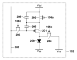
図2は、本実施形態における画素102の駆動回路の回路図を示す。画素102は、発光素子として有機EL素子200を含む。また、画素102は、駆動回路として、駆動トランジスタ201、発光制御トランジスタ202、書込トランジスタ203、リセットトランジスタ204の4つのトランジスタと、2つの静電容量205、206を含む。駆動回路は、電源電位Vdd、Vssに接続されている。これら、駆動回路を構成する4つのトランジスタは、それぞれP型トランジスタであり、制御信号は、3つの走査線106a、106b、106cを介して発光制御トランジスタ202、書込トランジスタ203、リセットトランジスタ204のゲート電極にそれぞれ入力される。
Figure 2 shows a circuit diagram of the driving circuit of the
信号線107は、書込トランジスタ203のソース領域に接続され、書込トランジスタ203がON状態となったときに、信号線107の電圧値が駆動トランジスタ201のゲート電極に入力される。この信号電圧に依存して駆動トランジスタ201のソース領域―ドレイン領域間を流れる電流値が決まり、有機EL素子200の発光輝度が制御される。駆動トランジスタ201のドレイン領域は、有機EL素子200のアノードおよびリセットトランジスタ204のソース領域に電気的に接続されている。リセットトランジスタ204がON状態である場合、有機EL素子200には電流が流れず、発光しない。発光制御トランジスタ202のソース領域は、電源電位Vddに接続され、ドレイン領域は、駆動トランジスタ201のソース領域に電気的に接続され、有機EL素子200の発光または非発光を制御する。有機EL素子200のカソードとリセットトランジスタのドレイン領域は、電源電位Vssに接続され同電位となっている。電源電位Vddは、電源電位Vssを基準として、例えば、+10ボルトであるが、これらの電位の設定は、発光素子である有機EL素子200の光電変換特性によって決定されるものである。
The
図3は、本実施形態における駆動回路を構成する駆動トランジスタ201、発光制御トランジスタ202、書込トランジスタ203、リセットトランジスタ204の基板上での配置を示す平面図である。図3の水平(横)方向をx方向、基板の表面上でx方向に垂直な方向(図3の縦方向)をy方向とする。発光制御トランジスタ202、駆動トランジスタ201およびリセットトランジスタ204は、ソース領域、ゲート領域およびドレイン領域がy方向に平行な直線上に並ぶ。書込トランジスタ203は、他の3つのトランジスタとはソース領域408、ドレイン領域410が絶縁体で分離され、ソース領域408、ゲート領域およびドレイン領域410が、y方向に平行に配置される。図2の回路において、発光制御トランジスタ202のドレイン領域と駆動トランジスタ201のソース領域は同電位であり、図3に示されるように同じ拡散領域413を共有する共有ノードとして配される。同様に、駆動トランジスタ201のドレイン領域とリセットトランジスタ204のソース領域は、同電位となることから、同じ拡散領域415を共有する共有ノードとして配される。書込トランジスタ203のドレイン領域410と駆動トランジスタ201のゲート電極414は、図2の回路図上は同一端子であるため、図3に示されるように配線パターン421を介して導通される。図3は、半導体基板上の平面図であるため、図2の回路図に示される結線は描かれていないが、半導体基板のそれぞれのトランジスタの上には配線層が積層され、配線パターンと貫通ビアによって図2に示される回路が実現される。断面構造については後に図4で示す。
3 is a plan view showing the arrangement on a substrate of the driving
本実施形態における発光装置101は、2次元的に配列された発光素子(有機EL素子200)に対応するように駆動回路が配されている。配置形態は発光素子の配列とは異なってもよいが、駆動回路は、少なくとも発光素子の配置密度と同等またはそれ以上に密に配列する。
In the light-emitting
図3に示される示す破線で囲まれたトランジスタ領域301、302、303、304は、半導体基板に対する正射影において、駆動回路を構成する4つのトランジスタの活性領域(ゲート領域)、ソース領域、ドレイン領域、および、ゲート電極(ゲート端子)が占める領域である。ソース領域、ドレイン領域は、例えば、ウェル層とは逆の導電型の領域として定義されてもよい。また、例えば、ソース領域、ドレイン領域は、トランジスタがオフ状態のときの活性領域とは逆の導電型の領域として定義されてもよい。また、例えば、ソース領域、ドレイン領域は、トランジスタがオフ状態のときの活性領域よりも、不純物濃度が10倍以上の領域として定義されてもよい。活性領域は、ゲート電極の下に形成され、ゲート電極の電位の変化に応じてソース領域とドレイン領域との間で電荷が転送される領域として定義されてもよい。活性領域は、チャネル領域とも呼ばれうる。ゲート電極は、例えば、ゲート電極を構成する導電パターンとして定義されてもよい。また、ゲート電極は、画素のレイアウトに応じて、種々の形状をとりうる。このため、トランジスタ領域は、半導体基板に対する正射影において、駆動回路を構成する複数のトランジスタの活性領域、ソース領域、および、ドレイン領域が占める領域であってもよい。それぞれのトランジスタ領域301~304に配されたトランジスタが、1つの有機EL素子200を駆動する回路を構成する。図3には、4つの画素102(4つの有機EL素子200)に対応する駆動回路を構成する複数のトランジスタが配されたトランジスタ領域が示されている。書込トランジスタ203は、駆動トランジスタ201、発光制御トランジスタ202、リセットトランジスタ204とは絶縁分離部を介して離れているが、書込トランジスタ203を含めて1つのトランジスタ領域301~304を構成する。
The
ここで、複数の画素102のうち、図3のy方向に互いに隣り合う画素102のトランジスタ領域の関係について説明する。換言すると、y方向に互いに隣り合うトランジスタ領域301とトランジスタ領域302との関係である。図3に示されるように、トランジスタ領域302を通過するy方向に平行な仮想線が、トランジスタ領域301を通過する。同義であるが、トランジスタ領域301のトランジスタ領域302の側の端部が、トランジスタ領域302のトランジスタ領域301の側の端部よりもy方向について図3の配置において上に配されている。トランジスタ領域301とトランジスタ領域302とが、x方向において重なる領域を備えることによって、駆動回路を構成する各トランジスタの配置密度を高めることが可能となる。これによって、トランジスタの微細化によらずに、発光装置101の高解像度化が可能となる。
Here, the relationship between the transistor regions of the
本実施形態において、トランジスタ領域301~304のそれぞれに配される複数のトランジスタのうちソース領域、ゲート領域およびドレイン領域がy方向に平行な仮想線VL1(第1群仮想線)に沿って配されたトランジスタを第1群のトランジスタと呼ぶ。具体的には、駆動トランジスタ201、発光制御トランジスタ202、リセットトランジスタ204のことを第1群のトランジスタと呼ぶ。トランジスタ領域301~304のそれぞれに配される複数のトランジスタのうちソース領域、ゲート領域およびドレイン領域が仮想線VL1に平行な仮想線VL2(第2群仮想線)に沿って配されたトランジスタを第2群のトランジスタと呼ぶ。具体的には、書込トランジスタ203のことを第2群のトランジスタと呼ぶ。トランジスタ領域301~304のそれぞれに配される複数のトランジスタは、それぞれ1つ以上のトランジスタを含む第1群と第2群とを構成している。
In this embodiment, among the multiple transistors arranged in each of the
第1群および第2群のトランジスタは、ソース領域、ゲート領域およびドレイン領域がy方向に平行に配され、図3に示されるように、第1群のトランジスタのゲート電極412、414、416を通過するx方向に沿った仮想線が、第2群のトランジスタのゲート電極409を通過しない。図3において、ゲート電極は、斜線で示される領域である。例えば、同じトランジスタ領域302に配される第1群のトランジスタのゲート電極412、414、416を通過するx方向に平行な仮想線が、第2群のトランジスタのゲート電極409を通過しない。また、例えば、トランジスタ領域302に配される第1群のトランジスタのゲート電極412、414、416を通過するx方向に平行な仮想線が、トランジスタ領域301に配される第2群のトランジスタのゲート電極409を通過しない。
The source regions, gate regions, and drain regions of the first and second groups of transistors are arranged parallel to the y direction, and as shown in FIG. 3, an imaginary line along the x direction passing through the
図3に示されるようなトランジスタの形状の場合、それぞれのトランジスタのゲート電極間の距離がトランジスタの配置密度を決める場合がある。ゲート電極同士がx方向において対向しないように、それぞれのトランジスタを配置することによって、図3のx方向の駆動回路の配列密度を、さらに高めることができる。ただし、図3のy方向については、駆動回路が長く伸びる配置になるため、y方向に隣り合うトランジスタ領域(例えばトランジスタ領域302)の下端部が、トランジスタ領域301に配される書込トランジスタ203のソース領域408の位置よりも下側に配し、かつ、トランジスタ領域301とトランジスタ領域302との各ゲート電極が対向しないように配置されることで、y方向にも駆動回路の最密配置を可能にする。図3に示される構成において、トランジスタ領域302に配された発光制御トランジスタ202のソース領域418を通過するx方向に平行な仮想線が、トランジスタ領域301の書込トランジスタ203のゲート電極409を通過する。
In the case of a transistor shape as shown in FIG. 3, the distance between the gate electrodes of each transistor may determine the arrangement density of the transistors. By arranging each transistor so that the gate electrodes do not face each other in the x direction, the arrangement density of the drive circuit in the x direction of FIG. 3 can be further increased. However, in the y direction of FIG. 3, the drive circuit is arranged to extend longer, so that the lower end of the transistor region (e.g., transistor region 302) adjacent in the y direction is arranged below the position of the
本実施形態において、3色の発光素子が配される例を想定しているため、駆動回路が配されるトランジスタ領域301~304のx方向の配置間隔とy方向の配置間隔の比は1:3である。これによって、3色の画素102を1つの「表示画素」としたとき、x方向とy方向との「表示画素」の配列間隔が等しくなる。つまり、1つの有機EL素子200に対応する駆動回路が配されるトランジスタ領域301~304のそれぞれを1つの画素102の領域とすると、複数の画素102のうちy方向に配される画素102のピッチが、複数の画素102のうちx方向に配される画素102のピッチよりも広いと言える。また、ここで、x方向に互いに隣り合う2つの画素102に対応するトランジスタ領域(例えば、トランジスタ領域301およびトランジスタ領域303)に注目する。このとき、図3に示されるように、トランジスタ領域301をx方向に平行移動させた位置に、トランジスタ領域303が配されうる。
In this embodiment, since an example in which three-color light-emitting elements are arranged is assumed, the ratio of the arrangement interval in the x direction to the arrangement interval in the y direction of the
1つの発光素子である有機EL素子200を駆動する、駆動トランジスタ201、発光制御トランジスタ202、書込トランジスタ203、リセットトランジスタ204を含む駆動回路を上述のように配置する。これによって、基板上での駆動回路の各トランジスタの配置密度を高くすることが可能となる。これによって、トランジスタの微細化によらずに、発光素子である有機EL素子200の高密度化が実現可能となり、より高解像度な発光装置101が実現できる。
The drive circuit including the
図3に示したA―A’間における断面が、図4に示されている。図4は、本実施形態における駆動回路(駆動トランジスタ201、発光制御トランジスタ202、書込トランジスタ203、リセットトランジスタ204)、発光素子である有機EL素子200、配線層、および、静電容量205、206の断面構造例である。本実施形態における発光装置101は、半導体の基板401、基板401の上に形成される配線層402、発光素子層403を含み構成されている。基板401は単結晶のP型のシリコン基板407を基礎とし、N型ウェル層406が形成され、その上にトランジスタであるMOSFETが形成される。N型ウェル層406は電源電圧Vddに電気的に接続される。端子を共有しないトランジスタ間は絶縁体分離部405によって絶縁分離される。本実施形態において、絶縁体分離部405は、STI(Shallow Trench Isolation)構造によって実現される。絶縁体分離部405は、LOCOS(Local Oxidation Of Silicon)分離やDeep Trench Isolation (DTI)、N型の拡散層分離などにも置換可能である。本実施形態におけるSTI構造は、酸化シリコンを用いて、基板401の表面から0.3ミクロンから1.0ミクロン程度の深さまで形成される。駆動トランジスタ201、発光制御トランジスタ202、書込トランジスタ203、リセットトランジスタ204は、基板401上に形成された薄い絶縁膜上にポリシリコンのゲート電極414、412、409、416をそれぞれ備える。駆動トランジスタ201、発光制御トランジスタ202、書込トランジスタ203、リセットトランジスタ204のソース領域およびドレイン領域は、P型の拡散層によって形成され、配線層とは貫通ビアによって電気的に接続されている。
The cross section between A-A' shown in FIG. 3 is shown in FIG. 4. FIG. 4 shows an example of the cross-sectional structure of the drive circuit (drive
図2に示される電源Vddの電源電圧は、複数のパターニングされた金属層とそれらの層を電気的に接続する貫通ビアを含む絶縁層で構成される配線層402を介して発光制御トランジスタ202のソース領域411に供給される。配線層402は、配線パターンの他に、静電容量205、206を構成する上部電極パターン442、445および薄膜の絶縁層443、446を含む。これら静電容量205、206を構成する薄膜の絶縁層443、446の厚さは数十ナノメートル程度である。配線層402の金属配線パターン、およびビアには、タングステン、モリブデン、チタン、アルミニウム、ネオジウム、クロム、コバルト、銅、金やこれらの積層、化合物および合金や、シリコンや銅などの金属との化合物および合金が用いられうる。また、配線層402の絶縁層には、酸化シリコンや窒化シリコンが用いられうる。
2 is supplied to the
配線層402の上部には、発光素子層403が形成される。発光素子層403は、有機EL素子200のアノード451、有機発光層452、カソード453、バンク部454を含み構成される。バンク部454は、隣接する画素102(発光素子)間の電気的なクロストークを抑制する働きを有する。発光方向は図4において上部方向であり、カソード453は、発光波長領域で十分な光透過性がある。
A light emitting
走査線106aを介した走査信号は、配線層402内部の配線パターンを介して発光制御トランジスタ202のゲート電極412に入力され、発光制御トランジスタ202を制御する。発光制御トランジスタ202がON状態のとき、駆動トランジスタ201のソース領域(拡散領域413)に電源電位Vddが印可される。
The scanning signal via the scanning line 106a is input to the
走査線106bを介した走査信号は、配線層402内部の配線パターンを介して書込トランジスタ203のゲート電極412に入力され、書込トランジスタ203を制御する。書込トランジスタ203がON状態のとき、駆動トランジスタ201のゲート電極414に信号線107を介した信号電位が印可される。書込トランジスタ203は、駆動トランジスタ201と絶縁体分離部405で絶縁されているため、書込トランジスタ203のドレイン領域410と駆動トランジスタ201のゲート電極414とは、配線層402内の配線パターン421を介して接続している。駆動トランジスタ201のゲート電極414の電位によって、駆動トランジスタ201のドレイン電流、つまり、発光素子である有機EL素子200に流れる電流が制御され、発光輝度が決まる。駆動トランジスタ201のドレイン領域(拡散領域415)は、有機EL素子200のアノード451に配線層402内の配線パターンなどを介して接続されている。
The scanning signal through the
走査線106cを介した走査信号は、配線層402内部の配線パターンを介してリセットトランジスタ204のゲート電極416に入力され、リセットトランジスタ204を制御する。リセットトランジスタ204がON状態のとき、リセットトランジスタ204のソース領域(拡散領域415)に導通しているアノード451が、電源電圧Vssとなる。有機EL素子200のカソード453は、すべての有機EL素子200に共通の電極でありうり、電源電位Vssが供給されている。したがって、リセットトランジスタ204がON状態のとき、有機EL素子200のアノード451とカソード453とが等電位となり、発光が停止し、有機EL素子200はリセットされる。
The scanning signal via the
図5、6は、駆動トランジスタ201、発光制御トランジスタ202、書込トランジスタ203、リセットトランジスタ204を含む駆動回路の図3に示される配置に対する変形例である。図3に示す構成では、トランジスタ領域302において、トランジスタ領域301の側から発光制御トランジスタ202、駆動トランジスタ201、リセットトランジスタ204の順に並んでいる。一方、図5に示す構成において、トランジスタ領域312において、トランジスタ領域311の側からリセットトランジスタ204、駆動トランジスタ201、発光制御トランジスタ202の順に並んでいる。
Figures 5 and 6 show modified examples of the arrangement of the drive circuit including the
ここで、y方向に互いに隣り合う2つの画素102に対応するトランジスタ領域(例えば、トランジスタ領域311およびトランジスタ領域312)に注目する。図5に示される構成において、トランジスタ領域312に配されたリセットトランジスタ204のドレイン領域471を通過するx方向に平行な仮想線が、トランジスタ領域311の書込トランジスタ203のゲート電極462を通過する。また、トランジスタ領域311の書込トランジスタ203のゲート電極462を通過するx方向に平行な仮想線が、トランジスタ領域311に配される第1群のトランジスタ(駆動トランジスタ201、発光制御トランジスタ202、リセットトランジスタ204)のゲート電極465、467、469を通過しない。また、トランジスタ領域311の書込トランジスタ203のゲート電極462を通過するx方向に平行な仮想線が、トランジスタ領域312に配される第1群のトランジスタ(駆動トランジスタ201、発光制御トランジスタ202、リセットトランジスタ204)のゲート電極を通過しない。この構成によって、図3に示さる構成と同様に、発光素子である有機EL素子200を駆動する駆動回路を高密度に配置することが可能となる。これによって、図5に示される構成においても、発光装置101の高解像度化が可能となる。
Here, attention is paid to the transistor regions (for example, the
図5に示したB―B’間における断面が、図6に示される。各層の構成および材料などは、上述の図4に示される断面と同様でありうるが、発光制御トランジスタ202およびリセットトランジスタ204の配列が異なる。それに伴い、配線層402の構成も一部、異なっている。発光素子である有機EL素子200の構造は、図4の構成と同等でありうる。
The cross section between B-B' shown in FIG. 5 is shown in FIG. 6. The configuration and materials of each layer may be similar to those of the cross section shown in FIG. 4 described above, but the arrangement of the light-emitting
走査線106aを介した走査信号は、配線層402内部の配線パターンを介して発光制御トランジスタ202のゲート電極469に入力され、発光制御トランジスタ202を制御する。発光制御トランジスタ202がON状態のとき、駆動トランジスタ201のソース領域468に電源電位Vddが印可される。
The scanning signal via the scanning line 106a is input to the
走査線106bを介した走査信号は、配線層402内部の配線パターンを介して書込トランジスタ203のゲート電極462に入力され、書込トランジスタ203を制御する。書込トランジスタ203がON状態のとき、駆動トランジスタ201のゲート電極467に信号線107を介した信号電位が印可される。書込トランジスタ203は、駆動トランジスタ201と絶縁体分離部405で絶縁されているため、書込トランジスタ203のドレイン領域463と駆動トランジスタ201のゲート電極467とは、配線層402内の配線パターン421を介して接続している。駆動トランジスタ201のゲート電極467の電位によって、駆動トランジスタ201のドレイン電流、つまり、発光素子である有機EL素子200に流れる電流が制御され、発光輝度が決まる。駆動トランジスタ201のドレイン領域(拡散領域466)は、発光素子200のアノード451に配線層402内の配線パターンなどを介して接続されている。
The scanning signal through the
走査線106cを介した走査信号は、配線層402内部の配線パターンを介してリセットトランジスタ204のゲート電極465に入力され、リセットトランジスタ204を制御する。リセットトランジスタ204がON状態のとき、リセットトランジスタ204のソース領域(拡散領域466)に導通しているアノード451が、電源電圧Vssとなる。有機EL素子200のカソード453は、すべての有機EL素子200に共通の電極でありうり、電源電位Vssが供給されている。したがって、リセットトランジスタ204がON状態のとき、有機EL素子200のアノード451とカソード453とが等電位となり、発光が停止し、有機EL素子200はリセットされる。
The scanning signal via the
図5に示される構成において、駆動トランジスタ201、発光制御トランジスタ202、リセットトランジスタ204の位置が、図3に示される構成に対して反転した位置に配されている。しかしこれに限られることはなく、例えば、図5に示される構成において、書込トランジスタ203のソース領域408およびドレイン領域410が、反転していてもよい。図3に示される構成においても、書込トランジスタ203のソース領域408およびドレイン領域410が、反転していてもよい。
In the configuration shown in FIG. 5, the positions of the
図7は、駆動トランジスタ201、発光制御トランジスタ202、書込トランジスタ203、リセットトランジスタ204を含む駆動回路の図3、5に示される配置に対するさらなる変形例である。図7に示される構成は、トランジスタ領域321~324の配置を1行ずつ、交互にミラー対称に配置させたものである。
Figure 7 shows a further modification of the arrangement of the drive circuit including the
図7に示される構成において、N行目のトランジスタ領域321には、トランジスタ領域322の側から発光制御トランジスタ202、駆動トランジスタ201、リセットトランジスタ204の順でトランジスタが配されている。一方、N+1行目のトランジスタ領域322には、トランジスタ領域322の側から発光制御トランジスタ202、駆動トランジスタ201、リセットトランジスタ204の順でトランジスタが配されている。
In the configuration shown in FIG. 7, in the
このとき、y方向に互いに隣り合う2つの画素102のトランジスタ領域(例えば、トランジスタ領域321およびトランジスタ領域322。)において、トランジスタ領域321の発光制御トランジスタ202のソース領域と、トランジスタ領域322の発光制御トランジスタ202のソース領域と、が1つの拡散領域480を共有していてもよい。この場合、トランジスタ領域321とトランジスタ領域322との境界が、拡散領域480上を通過する。したがって、トランジスタ領域321の発光制御トランジスタ202のソース領域およびトランジスタ領域322の発光制御トランジスタ202のソース領域を通過するx方向に平行な仮想線が、トランジスタ領域322の書込トランジスタ203のゲート電極を通過する。
In this case, in the transistor regions (e.g.,
また、同様に、y方向に互いに隣り合う2つの画素102のトランジスタ領域において、リセットトランジスタ204のドレイン領域も同電位の電源電圧Vssに接続されるため、拡散領域を共有していてもよい。この場合、y方向に互いに隣り合う2つの画素102のトランジスタ領域の境界が、リセットトランジスタ204のドレイン領域として機能する共有された拡散領域上を通過する。したがって、y方向に互いに隣り合う2つの画素102のトランジスタ領域321の発光制御トランジスタ202の拡散領域を共有するソース領域を通過するx方向に平行な仮想線が、何れかのトランジスタ領域の書込トランジスタ203のゲート電極を通過する。
Similarly, in the transistor regions of two
図7に示される構成において、図3、5に示されるように駆動回路を画素102ごとに絶縁分離する必要がなくなる。このため、さらなる駆動回路の最密配置が可能になり、発光装置101の高解像度化が可能となる。
In the configuration shown in FIG. 7, it is no longer necessary to insulate and separate the driving circuits for each
図8は、図2に示す画素102の駆動回路の変形例を示す図である。図8に示される構成は、図2に示される構成と比較して、リセットトランジスタ204が配されていない構成となっている。これ以外の構成は、図2に示す構成と同様であってもよい。
Figure 8 is a diagram showing a modified example of the drive circuit of the
具体的には、画素102は、発光素子として有機EL素子600を含む。また、画素102は、駆動回路として、駆動トランジスタ601、発光制御トランジスタ602、書込トランジスタ603の3つのトランジスタと、2つの静電容量605、606を含む。駆動回路は、電源電位Vdd、Vssに接続されている。これら、駆動回路を構成する4つのトランジスタは、それぞれP型トランジスタであり、制御信号は、2つの走査線106a、106bを介して発光制御トランジスタ202、書込トランジスタ203のゲート電極にそれぞれ入力される。
Specifically, the
信号線107は、書込トランジスタ603のドレイン領域に接続され、書込トランジスタ603がON状態となったときに、信号線107の電圧値が駆動トランジスタ601のゲート電極に入力される。この信号電圧に依存して駆動トランジスタ601のソース端子―ドレイン端子間を流れる電流値が決まり、有機EL素子600の発光輝度が制御される。駆動トランジスタ701のドレイン端子は有機EL素子700のアノードに電気的に接続している。電源電位Vddは電源電位Vssを基準として+10ボルトであるが、これらの電位の設定は発光素子である有機EL素子600の光電変換特性によって決定されるものである。
The
図9は、図8に示される駆動回路を構成する駆動トランジスタ601、発光制御トランジスタ602、書込トランジスタ603の基板上での配置を示す平面図である。発光制御トランジスタ602、および、駆動トランジスタ601は、ソース領域、ゲート領域およびドレイン領域がy方向に平行な直線上に並ぶ。書込トランジスタ603は、発光制御トランジスタ602、および、駆動トランジスタ601とはソース領域616、ドレイン領域618が絶縁体で分離され、ソース領域616、ゲート領域およびドレイン領域618がy方向に平行に配置される。図8の回路において、発光制御トランジスタ602のドレイン領域と駆動トランジスタ601のソース領域は同電位であり、図9に示されるように同じ拡散領域613を共有する共有ノードとして配される。書込トランジスタ603のドレイン領域と駆動トランジスタ601のゲート電極は、図8の回路図上は同一端子であるため、図9に示されるように配線パターン619を介して導通される。図9は、半導体基板上の平面図であるため、図8の回路図に示される結線は描かれていないが、半導体基板のそれぞれのトランジスタの上には配線層が積層され、配線パターンと貫通ビアによって図8に示される回路が実現される。
Figure 9 is a plan view showing the arrangement on a substrate of the driving
ここで、y方向に互いに隣り合う2つの画素102に対応するトランジスタ領域(例えば、トランジスタ領域331およびトランジスタ領域332)に注目する。図9に示される構成において、トランジスタ領域332に配された発光制御トランジスタ602のドレイン領域620を通過するx方向に平行な仮想線が、トランジスタ領域331の書込トランジスタ603のゲート電極617を通過する。また、トランジスタ領域311の書込トランジスタ603のゲート電極617を通過するx方向に平行な仮想線が、トランジスタ領域331に配される第1群のトランジスタ(駆動トランジスタ601、発光制御トランジスタ602)のゲート電極612、613を通過しない。また、トランジスタ領域311の書込トランジスタ603のゲート電極617を通過するx方向に平行な仮想線が、トランジスタ領域332に配される第1群のトランジスタ(駆動トランジスタ601、発光制御トランジスタ602)のゲート電極を通過しない。この構成によって、上述の各構成と同様に、発光素子である有機EL素子600を駆動する駆動回路を高密度に配置することが可能となる。これによって、図9に示される構成においても、発光装置101の高解像度化が可能となる。
Here, attention is paid to the transistor regions (for example, the
図10は、駆動トランジスタ601、発光制御トランジスタ602、書込トランジスタ603を含む駆動回路の図9に示される配置に対する変形例である。図9に示す構成では、トランジスタ領域332において、トランジスタ領域331の側から発光制御トランジスタ602、駆動トランジスタ601の順に並んでいる。一方、図10に示す構成において、トランジスタ領域342において、トランジスタ領域341の側から駆動トランジスタ601、発光制御トランジスタ602の順に並んでいる。これ以外の構成は、図9の構成と同様であってもよいため、ここでは説明を省略する。図10に示される構成においても、図9に示される構成と同様の駆動回路の高密度化の効果が得られ、結果として発光装置101の高解像度化が可能となる。
Figure 10 is a modified example of the arrangement of the drive circuit including the
図10に示される構成において、駆動トランジスタ601、発光制御トランジスタ602の位置が、図9に示される構成に対して反転した位置に配されている。しかしこれに限られることはなく、例えば、図10に示される構成において、書込トランジスタ603のソース領域およびドレイン領域が、反転していてもよい。同様に、図9に示される構成においても、書込トランジスタ603のソース領域616およびドレイン領域618が、反転していてもよい。
In the configuration shown in FIG. 10, the positions of the
図11は、駆動トランジスタ601、発光制御トランジスタ602、書込トランジスタ603を含む駆動回路の図9、10に示される配置に対するさらなる変形例である。図11に示される構成は、トランジスタ領域351~354の配置を1行ずつ、交互にミラー対称に配置させたものである。
Figure 11 shows a further modification of the arrangement of the drive circuit including the
図11に示される構成において、N行目のトランジスタ領域351には、トランジスタ領域352の側から発光制御トランジスタ602、駆動トランジスタ601の順でトランジスタが配されている。一方、N+1行目のトランジスタ領域352には、トランジスタ領域352の側から発光制御トランジスタ602、駆動トランジスタ601の順でトランジスタが配されている。
In the configuration shown in FIG. 11, in the
このとき、y方向に互いに隣り合う2つの画素102のトランジスタ領域(例えば、トランジスタ領域351およびトランジスタ領域352。)において、トランジスタ領域351の発光制御トランジスタ602のソース領域と、トランジスタ領域352の発光制御トランジスタ602のソース領域と、が1つの拡散領域621を共有していてもよい。この場合、トランジスタ領域351とトランジスタ領域352との境界が、拡散領域621上を通過する。したがって、トランジスタ領域351の発光制御トランジスタ602のソース領域およびトランジスタ領域352の発光制御トランジスタ602のソース領域を通過するx方向に平行な仮想線が、トランジスタ領域352の書込トランジスタ603のゲート電極を通過する。
At this time, in the transistor regions (e.g.,
図11に示される構成において、図9、10に示されるように駆動回路を画素102ごとに絶縁分離する必要がなくなる。このため、さらなる駆動回路の最密配置が可能になり、発光装置101の高解像度化が可能となる。
In the configuration shown in FIG. 11, it is no longer necessary to insulate and separate the driving circuits for each
図12は、図2、8に示す画素102の駆動回路の変形例を示す図である。図10に示される構成は、図2に示される構成と比較して、発光制御トランジスタ202、リセットトランジスタ204が配されていない構成となっている。また、発光制御トランジスタ202が配されないため、静電容量206も配されていない。これ以外の構成は、図2に示す構成と同様であってもよい。
Figure 12 is a diagram showing a modified example of the drive circuit of the
具体的には、画素102は、発光素子として有機EL素子700を含む。また、画素102は、駆動回路として、駆動トランジスタ701、書込トランジスタ703の2つのトランジスタと、1つの静電容量705を含む。駆動回路は、電源電位Vdd、Vssに接続されている。これら、駆動回路を構成する2つのトランジスタは、それぞれP型トランジスタであり、制御信号は、走査線106bを介して書込トランジスタ703のゲート電極にそれぞれ入力される。
Specifically,
信号線107は、書込トランジスタ703のドレイン領域に接続され、書込トランジスタ703がON状態となったときに、信号線107の電圧値が駆動トランジスタ701のゲート電極に入力される。この信号電圧に依存して駆動トランジスタ701のソース端子―ドレイン端子間を流れる電流値が決まり、有機EL素子700の発光輝度が制御される。駆動トランジスタ701のドレイン端子は有機EL素子700のアノード端子に接続している。電源電位Vddは電源電位Vssを基準として+10ボルトであるが、これらの電位の設定は発光素子である有機EL素子700の光電変換特性によって決定されるものである。
The
図13は、図12の変形例である。上述の各構成において、画素102の駆動回路に用いられるトランジスタとしてP型トランジスタを用いる例を示した。しかしながら、これに限られることはない。図13には、駆動トランジスタ801および書込トランジスタ803が、N型トランジスタによって構成される例が示されている。したがって、静電容量805は駆動トランジスタ801のゲート-ソース間に接続されている。上述の各構成においても、P型トランジスタに代えてN型トラジスタが用いられていてもよい。
Figure 13 is a modified example of Figure 12. In each of the above configurations, an example has been shown in which a P-type transistor is used as the transistor used in the drive circuit of
図14は、図12に示される駆動回路を構成する駆動トランジスタ701、書込トランジスタ703の基板上での配置を示す平面図である。図14は、図12の回路図と対応付けて説明するが、図13の回路図ともトランジスタのP-Nの極性が異なることを除いて、トランジスタの配置は同様でありうる。駆動トランジスタ701は、ソース領域、ゲート領域およびドレイン領域がy方向に平行な直線上に並ぶ。書込トランジスタ603は、駆動トランジスタ601とはソース領域、ドレイン領域が絶縁体で分離され、ソース領域、ゲート領域およびドレイン領域がy方向に平行に配置される。書込トランジスタ603のドレイン領域と駆動トランジスタ601のゲート電極は、図8の回路図上は同一端子であるため、図9に示されるように配線パターンを介して導通される。図9は、半導体基板上の平面図であるため、図8の回路図に示される結線は描かれていないが、半導体基板のそれぞれのトランジスタの上には配線層が積層され、配線パターンと貫通ビアによって図8に示される回路が実現される。
Figure 14 is a plan view showing the arrangement on a substrate of the
ここで、y方向に互いに隣り合う2つの画素102に対応するトランジスタ領域(例えば、トランジスタ領域371およびトランジスタ領域372)に注目する。図14に示される構成において、トランジスタ領域372に配された駆動トランジスタ701のドレイン領域またはソース領域を通過するx方向に平行な仮想線が、トランジスタ領域371の書込トランジスタ703のゲート電極を通過する。また、トランジスタ領域371の書込トランジスタ703のゲート電極を通過するx方向に平行な仮想線が、トランジスタ領域371に配される第1群のトランジスタ(駆動トランジスタ701)のゲート電極を通過しない。また、トランジスタ領域371の書込トランジスタ703のゲート電極を通過するx方向に平行な仮想線が、トランジスタ領域372に配される第1群のトランジスタ(駆動トランジスタ701)のゲート電極を通過しない。この構成によって、上述の各構成と同様に、発光素子である有機EL素子700を駆動する駆動回路を高密度に配置することが可能となる。これによって、図14に示される構成においても、発光装置101の高解像度化が可能となる。
Here, attention is paid to the transistor regions (for example, the
図15は、図14に示される駆動回路を構成する駆動トランジスタ701、書込トランジスタ703の基板上での配置の変形例を示す平面図である。図15に示す構成において、駆動トランジスタ701および書込トランジスタ703がy方向に平行な直線上に並んでいる。また、x方向に互いに隣り合う駆動トランジスタ701および書込トランジスタ703が互いのゲート端子が対向しないようにy方向に互い違いに配されている。
Figure 15 is a plan view showing a modified arrangement on a substrate of the
ここで、y方向に互いに隣り合う2つの画素102に対応するトランジスタ領域(例えば、トランジスタ領域381およびトランジスタ領域382。)、および、y方向に互いに隣り合う2つの画素102に対してx方向に互いに隣り合う画素102に対応するトランジスタ領域(例えば、トランジスタ領域383。)に注目する。このとき、トランジスタ領域383を通過するx方向に平行な仮想線が、トランジスタ領域381、または、トランジスタ領域382を通過する。さらに、トランジスタ領域383の複数のトランジスタのゲート電極を通過するx方向に平行な仮想線が、トランジスタ領域381およびトランジスタ領域381の複数のトランジスタのゲート電極を通過しない。これによって、x方向およびy方向にも高密度に駆動回路を配置できる。図15に示される構成においても、発光装置101の高解像度化が可能となる。
Here, attention is paid to the transistor regions (e.g.,
ここで、本実施形態の発光装置101を表示装置、光電変換装置、電子機器、照明装置、移動体、ウェアラブルデバイスに適用した応用例について図16~22を用いて説明する。他にも、発光装置101には、電子写真方式の画像形成装置の露光光源や液晶表示装置のバックライト、白色光源にカラーフィルタを有する発光デバイスなどの用途がある。表示装置は、エリアCCD、リニアCCD、メモリーカード等からの画像情報を入力する画像入力部を有し、入力された情報を処理する情報処理部を有し、入力された画像を表示部に表示する画像情報処理装置でもよい。また、カメラやインクジェットプリンタが有する表示部は、タッチパネル機能を有していてもよい。このタッチパネル機能の駆動方式は、赤外線方式でも、静電容量方式でも、抵抗膜方式であっても、電磁誘導方式であってもよく、特に限定されない。また表示装置はマルチファンクションプリンタの表示部に用いられてもよい。
Here, application examples in which the light-emitting
図16は、本実施形態の発光装置101を用いた表示装置の一例を表す模式図である。表示装置1000は、上部カバー1001と、下部カバー1009と、の間に、タッチパネル1003、表示パネル1005、フレーム1006、回路基板1007、バッテリー1008を有していてもよい。タッチパネル1003および表示パネル1005は、フレキシブルプリント回路FPC1002、1004が接続されている。回路基板1007には、トランジスタなどの能動素子が配される。バッテリー1008は、表示装置1000が携帯機器でなければ、設けなくてもよいし、携帯機器であっても、この位置に設ける必要はない。表示パネル1005に、上述の発光装置101が適用できる。表示パネル1005として機能する発光装置101は、回路基板1007に配されたトランジスタなどの能動素子と接続され動作する。
Figure 16 is a schematic diagram showing an example of a display device using the light-emitting
図16に示される表示装置1000は、複数のレンズを有する光学部と、当該光学部を通過した光を受光し電気信号に光電変換する撮像素子とを有する光電変換装置(撮像装置)の表示部に用いられてもよい。光電変換装置は、撮像素子が取得した情報を表示する表示部を有してもよい。また、表示部は、光電変換装置の外部に露出した表示部であっても、ファインダ内に配置された表示部であってもよい。光電変換装置は、デジタルカメラ、デジタルビデオカメラであってもよい。
The
図17は、本実施形態の発光装置101を用いた光電変換装置の一例を表す模式図である。光電変換装置1100は、ビューファインダ1101、背面ディスプレイ1102、操作部1103、筐体1104を有してよい。光電変換装置1100は、撮像装置とも呼ばれうる。表示部であるビューファインダ1101に、上述の発光装置101が適用できる。この場合、発光装置101は、撮像する画像のみならず、環境情報、撮像指示などを表示してもよい。環境情報には、外光の強度、外光の向き、被写体の動く速度、被写体が遮蔽物に遮蔽される可能性などであってよい。
Figure 17 is a schematic diagram showing an example of a photoelectric conversion device using the light-emitting
撮像に適するタイミングはわずかな時間である場合が多いため、少しでも早く情報を表示した方がよい。したがって、発光素子として有機EL素子200などの有機発光材料を含む発光装置101がビューファインダ1101に用いられうる。有機発光材料は応答速度が速いためである。有機発光材料を用いた発光装置101は、表示速度が求められる、これらの装置に、液晶表示装置よりも適して用いることができる。
Since the timing suitable for capturing an image is often very short, it is better to display information as soon as possible. Therefore, a light-emitting
光電変換装置1100は、不図示の光学部を有する。光学部は複数のレンズを有し、光学部を通過した光を受光する筐体1104内に収容されている光電変換素子(不図示)に結像する。複数のレンズは、その相対位置を調整することで、焦点を調整することができる。この操作を自動で行うこともできる。
The
発光装置101、は、電子機器の表示部に適用されてもよい。その際には、表示機能と操作機能との双方を有してもよい。携帯端末としては、スマートフォンなどの携帯電話、タブレット、ヘッドマウントディスプレイなどが挙げられる。
The light-emitting
図18は、本実施形態の発光装置101を用いた電子機器の一例を表す模式図である。電子機器1200は、表示部1201と、操作部1202と、筐体1203を有する。筐体1203には、回路、当該回路を有するプリント基板、バッテリー、通信部、を有してよい。操作部1202は、ボタンであってもよいし、タッチパネル方式の反応部であってもよい。操作部1202は、指紋を認識してロックの解除等を行う、生体認識部であってもよい。通信部を有する携帯機器は通信機器ということもできる。表示部1201に、上述の発光装置101が適用できる。
Figure 18 is a schematic diagram showing an example of an electronic device using the light-emitting
図19(a)、19(b)は、本実施形態の発光装置101を用いた表示装置の一例を表す模式図である。図19(a)は、テレビモニタやPCモニタなどの表示装置である。表示装置1300は、額縁1301を有し表示部1302を有する。表示部1302に、上述の発光装置101、が適用できる。表示装置1300は、額縁1301と表示部1302とを支える土台1303を有していてもよい。土台1303は、図19(a)の形態に限られない。例えば、額縁1301の下辺が土台1303を兼ねていてもよい。また、額縁1301および表示部1302は、曲がっていてもよい。その曲率半径は、5000mm以上6000mm以下であってよい。
19(a) and 19(b) are schematic diagrams showing an example of a display device using the light-emitting
図19(b)は、本実施形態の発光装置101を用いた表示装置の他の例を表す模式図である。図19(b)の表示装置1310は、折り曲げ可能に構成されており、いわゆるフォルダブルな表示装置である。表示装置1310は、第1表示部1311、第2表示部1312、筐体1313、屈曲点1314を有する。第1表示部1311と第2表示部1312とには、上述の発光装置101が適用できる。第1表示部1311と第2表示部1312とは、つなぎ目のない1枚の表示装置であってよい。第1表示部1311と第2表示部1312とは、屈曲点で分けることができる。第1表示部1311と第2表示部1312とは、それぞれ異なる画像を表示してもよいし、第1表示部と第2表示部とで1つの画像を表示してもよい。
19(b) is a schematic diagram showing another example of a display device using the light-emitting
図20は、本実施形態の発光装置101を用いた照明装置の一例を表す模式図である。照明装置1400は、筐体1401と、光源1402と、回路基板1403と、光学フィルム1404と、光拡散部1405と、を有していてもよい。光源1402には、上述の発光装置101が適用できる。光学フィルム1404は光源の演色性を向上させるフィルタであってよい。光拡散部1405は、ライトアップなど、光源の光を効果的に拡散し、広い範囲に光を届けることができる。必要に応じて、最外部にカバーを設けてもよい。照明装置1400は、光学フィルム1404と光拡散部1405との両方を有していてもよいし、何れか一方のみを有していてもよい。
Figure 20 is a schematic diagram showing an example of an illumination device using the light-emitting
照明装置1400は例えば室内を照明する装置である。照明装置1400は白色、昼白色、その他青から赤のいずれの色を発光するものであってよい。それらを調光する調光回路を有してよい。照明装置1400は、光源1402として機能する発光装置101に接続される電源回路を有していてもよい。電源回路は、交流電圧を直流電圧に変換する回路である。また、白とは色温度が4200Kで昼白色とは色温度が5000Kである。また、照明装置1400は、カラーフィルタを有してもよい。また、照明装置1400は、放熱部を有していてもよい。放熱部は装置内の熱を装置外へ放出するものであり、比熱の高い金属、液体シリコンなどが挙げられる。
The
図21は、本実施形態の発光装置101を用いた車両用の灯具の一例であるテールランプを有する自動車の模式図である。自動車1500は、テールランプ1501を有し、ブレーキ操作などを行った際に、テールランプ1501を点灯する形態であってもよい。本実施形態の発光装置101は、車両用の灯具としてヘッドランプに用いられてもよい。自動車は移動体の一例であり、移動体は船舶やドローン、航空機、鉄道車両などであってもよい。移動体は、機体とそれに設けられた灯具を有してよい。灯具は機体の現在位置を知らせるものであってもよい。
Fig. 21 is a schematic diagram of an automobile having a tail lamp, which is an example of a vehicle lamp using the light-emitting
テールランプ1501に、上述の発光装置101が適用できる。テールランプ1501は、テールランプ1501として機能する発光装置101を保護する保護部材を有してよい。保護部材は、ある程度高い強度を有し、透明であれば材料は問わないが、ポリカーボネートなどで構成されてもよい。また、保護部材は、ポリカーボネートにフランジカルボン酸誘導体、アクリロニトリル誘導体などを混ぜてよい。
The above-described light
自動車1500は、車体1503、それに取り付けられている窓1502を有してもよい。窓は、自動車の前後を確認するための窓であってもよいし、透明なディスプレイであってもよい。当該透明なディスプレイは、有機層305の発光層が有機発光材料を含み発光装置として機能する上述の発光装置101が用いられてもよい。この場合、発光装置101が有する電極などの構成材料は透明な部材で構成される。
The
図22(a)、22(b)を参照して、上述の各実施形態の発光装置101のさらなる適用例について説明する。発光装置101は、例えばスマートグラス、HMD、スマートコンタクトのようなウェアラブルデバイスとして装着可能なシステムに適用できる。このような適用例に使用される撮像表示装置は、可視光を光電変換可能な撮像装置と、可視光を発光可能な発光装置とを有する。
With reference to Figures 22(a) and 22(b), further application examples of the light-emitting
図13(a)は、1つの適用例に係る眼鏡1600(スマートグラス)を説明する。眼鏡1600のレンズ1601の表面側に、CMOSセンサやSPADのような撮像装置1602が設けられている。また、レンズ1601の裏面側には、上述した各実施形態の発光装置101が設けられている。
Figure 13 (a) illustrates glasses 1600 (smart glasses) according to one application example. An
眼鏡1600は、制御装置1603をさらに備える。制御装置1603は、撮像装置1602と各実施形態に係る発光装置101に電力を供給する電源として機能する。また、制御装置1603は、撮像装置1602と発光装置101の動作を制御する。レンズ1601には、撮像装置1602に光を集光するための光学系が形成されている。
The
図13(b)は、1つの適用例に係る眼鏡1610(スマートグラス)を説明する。眼鏡1610は、制御装置1612を有しており、制御装置1612に、撮像装置1602に相当する撮像装置と、発光装置101が搭載される。レンズ1611には、制御装置1612内の撮像装置と、発光装置101からの発光を投影するための光学系が形成されており、レンズ1611には画像が投影される。制御装置1612は、撮像装置および発光装置101に電力を供給する電源として機能するとともに、撮像装置および発光装置101の動作を制御する。制御装置1612は、装着者の視線を検知する視線検知部を有してもよい。視線の検知は赤外線を用いてよい。赤外発光部は、表示画像を注視しているユーザーの眼球に対して、赤外光を発する。発せられた赤外光の眼球からの反射光を、受光素子を有する撮像部が検出することで眼球の撮像画像が得られる。平面視における赤外発光部から表示部への光を低減する低減手段を有することで、画像品位の低下を低減する。
Figure 13 (b) describes glasses 1610 (smart glasses) according to one application example. The
赤外光の撮像により得られた眼球の撮像画像から表示画像に対するユーザーの視線を検出する。眼球の撮像画像を用いた視線検出には任意の公知の手法が適用できる。一例として、角膜での照射光の反射によるプルキニエ像に基づく視線検出方法を用いることができる。 The user's line of sight with respect to the displayed image is detected from an image of the eyeball obtained by capturing infrared light. Any known method can be used for line of sight detection using an image of the eyeball. As an example, a line of sight detection method based on the Purkinje image formed by reflection of irradiated light on the cornea can be used.
より具体的には、瞳孔角膜反射法に基づく視線検出処理が行われる。瞳孔角膜反射法を用いて、眼球の撮像画像に含まれる瞳孔の像とプルキニエ像とに基づいて、眼球の向き(回転角度)を表す視線ベクトルが算出されることにより、ユーザーの視線が検出される。 More specifically, gaze detection processing is performed based on the pupil-corneal reflex method. Using the pupil-corneal reflex method, a gaze vector that represents the direction (rotation angle) of the eyeball is calculated based on the pupil image and Purkinje image contained in the captured image of the eyeball, thereby detecting the user's gaze.
本発明の一実施形態に係る発光装置101は、受光素子を有する撮像装置を有し、撮像装置からのユーザーの視線情報に基づいて表示画像を制御してよい。
The light-emitting
具体的には、発光装置101は、視線情報に基づいて、ユーザーが注視する第1の視界領域と、第1の視界領域以外の第2の視界領域とを決定される。第1の視界領域、第2の視界領域は、発光装置101の制御装置が決定してもよいし、外部の制御装置が決定したものを受信してもよい。発光装置101の表示領域において、第1の視界領域の表示解像度を第2の視界領域の表示解像度よりも高く制御してよい。つまり、第2の視界領域の解像度を第1の視界領域よりも低くしてよい。
Specifically, the light-emitting
また、表示領域は、第1の表示領域、第1の表示領域とは異なる第2の表示領域とを有し、視線情報に基づいて、第1の表示領域および第2の表示領域から優先度が高い領域を決定される。第1の視界領域、第2の視界領域は、発光装置101の制御装置が決定してもよいし、外部の制御装置が決定したものを受信してもよい。優先度の高い領域の解像度を、優先度が高い領域以外の領域の解像度よりも高く制御してよい。つまり優先度が相対的に低い領域の解像度を低くしてよい。
The display area has a first display area and a second display area different from the first display area, and an area with a high priority is determined from the first display area and the second display area based on line-of-sight information. The first field of view area and the second field of view area may be determined by a control device of the light-emitting
なお、第1の視界領域や優先度が高い領域の決定には、AIを用いてもよい。AIは、眼球の画像と当該画像の眼球が実際に視ていた方向とを教師データとして、眼球の画像から視線の角度、視線の先の目的物までの距離を推定するよう構成されたモデルであってよい。AIプログラムは、発光装置101が有しても、撮像装置が有しても、外部装置が有してもよい。外部装置が有する場合は、通信を介して、発光装置101に伝えられる。
Note that AI may be used to determine the first field of view area and areas with high priority. The AI may be a model configured to estimate the angle of gaze and the distance to an object in the line of sight from the image of the eyeball, using as teacher data an image of the eyeball and the direction in which the eyeball in the image was actually looking. The AI program may be possessed by the light-emitting
視認検知に基づいて表示制御する場合、外部を撮像する撮像装置を更に有するスマートグラスに好ましく適用できる。スマートグラスは、撮像した外部情報をリアルタイムで表示することができる。 When display control is based on visual detection, it is preferably applicable to smart glasses that further include an imaging device that captures images of the outside world. The smart glasses can display captured external information in real time.
発明は上記実施形態に制限されるものではなく、発明の精神及び範囲から離脱することなく、様々な変更及び変形が可能である。従って、発明の範囲を公にするために請求項を添付する。 The invention is not limited to the above-described embodiment, and various modifications and variations are possible without departing from the spirit and scope of the invention. Therefore, the following claims are appended to disclose the scope of the invention.
101:発光装置、102:画素、301~304,311~314,321~324,331~334,341~344,351~354,371~374,381~388:トランジスタ領域 101: Light emitting device, 102: Pixel, 301-304, 311-314, 321-324, 331-334, 341-344, 351-354, 371-374, 381-388: Transistor region
Claims (22)
前記複数の画素のそれぞれは、発光素子と、前記発光素子を駆動するための駆動回路と、を含み、
前記基板は、前記駆動回路を構成する複数のトランジスタが配されたトランジスタ領域を備え、
前記トランジスタ領域は、前記複数のトランジスタのそれぞれの活性領域および端子が配置された領域であり、
前記複数の画素は、前記第1方向に互いに隣り合う第1画素と第2画素とを含み、
前記第1画素の前記トランジスタ領域を通過する前記第2方向に平行な仮想線が、前記第2画素の前記トランジスタ領域を通過し、
前記複数のトランジスタは、それぞれ1つ以上のトランジスタを含む第1群と第2群とを構成し、
前記複数のトランジスタのうち前記第1群のトランジスタは、ソース領域、ゲート領域およびドレイン領域が前記第1方向に平行な第1群仮想線に沿って配され、
前記複数のトランジスタのうち前記第2群のトランジスタは、ソース領域、ゲート領域およびドレイン領域が前記第1群仮想線に平行な第2群仮想線に沿って配され、
前記複数の画素のそれぞれにおいて、前記複数のトランジスタのうち前記第1群のトランジスタのゲート電極を通過する前記第2方向に平行な仮想線が、前記複数のトランジスタのうち前記第2群のトランジスタのゲート電極を通過しないことを特徴とする発光装置。 A light-emitting device having a plurality of pixels arranged on a substrate to form a plurality of columns parallel to a first direction and a plurality of rows parallel to a second direction perpendicular to the first direction,
Each of the plurality of pixels includes a light-emitting element and a drive circuit for driving the light-emitting element;
the substrate includes a transistor region in which a plurality of transistors constituting the drive circuit are arranged;
the transistor region is a region in which active regions and terminals of each of the plurality of transistors are disposed,
the plurality of pixels include a first pixel and a second pixel adjacent to each other in the first direction,
a virtual line parallel to the second direction, which passes through the transistor region of the first pixel , passes through the transistor region of the second pixel;
the plurality of transistors are divided into a first group and a second group each including one or more transistors;
The first group of transistors among the plurality of transistors has a source region, a gate region, and a drain region arranged along a first group imaginary line parallel to the first direction,
The second group of transistors among the plurality of transistors has a source region, a gate region, and a drain region arranged along a second group imaginary line parallel to the first group imaginary line,
A light-emitting device characterized in that, in each of the plurality of pixels, a virtual line parallel to the second direction that passes through a gate electrode of a transistor of the first group among the plurality of transistors does not pass through a gate electrode of a transistor of the second group among the plurality of transistors .
前記第1トランジスタのゲート電極と、前記第2トランジスタのドレイン領域と、が電気的に接続され、
前記第1トランジスタのドレイン領域と、前記発光素子のアノードと、が電気的に接続されていることを特徴とする請求項1乃至4の何れか1項に記載の発光装置。 the plurality of transistors includes a first transistor included in the first group and a second transistor included in the second group;
a gate electrode of the first transistor and a drain region of the second transistor are electrically connected to each other;
5. The light emitting device according to claim 1 , wherein a drain region of the first transistor and an anode of the light emitting element are electrically connected to each other.
前記第3トランジスタは、ドレイン領域が前記第1トランジスタのソース領域に電気的に接続され、前記発光素子の発光または非発光を制御することを特徴とする請求項5に記載の発光装置。 the plurality of transistors further includes a third transistor included in the first group;
6. The light emitting device according to claim 5 , wherein the third transistor has a drain region electrically connected to a source region of the first transistor and controls whether the light emitting element emits light or not.
前記第4トランジスタは、ソース領域が前記第1トランジスタのドレイン領域および前記発光素子のアノードに電気的に接続され、前記発光素子をリセットすることを特徴とする請求項6に記載の発光装置。 the plurality of transistors further includes a fourth transistor included in the first group;
7. The light emitting device according to claim 6 , wherein the fourth transistor has a source region electrically connected to the drain region of the first transistor and an anode of the light emitting element, and resets the light emitting element.
前記第1画素の前記トランジスタ領域を前記第2方向に平行移動させた位置に、前記第3画素の前記トランジスタ領域が配されていることを特徴とする請求項1乃至14の何れか1項に記載の発光装置。 the plurality of pixels further includes a third pixel adjacent to the first pixel in the second direction,
15. The light emitting device according to claim 1, wherein the transistor region of the third pixel is disposed at a position obtained by translating the transistor region of the first pixel in the second direction.
前記表示部は、前記撮像素子が撮像した画像を表示する表示部であり、かつ、請求項1乃至16の何れか1項に記載の発光装置を有することを特徴とする光電変換装置。 The imaging device includes an optical unit having a plurality of lenses, an image sensor that receives light that has passed through the optical unit, and a display unit that displays an image,
17. A photoelectric conversion device, comprising: the display unit for displaying an image captured by the imaging element; and the light-emitting device according to claim 1.
前記表示部は、請求項1乃至16の何れか1項に記載の発光装置を有することを特徴とする電子機器。 A display unit is provided in a housing, and a communication unit is provided in the housing and communicates with an external device.
17. An electronic device, comprising: a display unit comprising the light-emitting device according to claim 1.
前記光源は、請求項1乃至16の何れか1項に記載の発光装置を有することを特徴とする照明装置。 A lighting device having a light source and at least one of a light diffusion unit and an optical film,
17. An illumination device, characterized in that the light source comprises a light emitting device according to claim 1.
前記灯具は、請求項1乃至16の何れか1項に記載の発光装置を有することを特徴とする移動体。 A moving body having a body and a lighting device provided on the body,
A moving body, wherein the lighting device comprises the light emitting device according to claim 1 .
前記表示装置は、請求項1乃至16の何れか1項に記載の発光装置を有することを特徴とするウェアラブルデバイス。 A wearable device having a display device for displaying an image,
A wearable device, comprising: a display device comprising the light-emitting device according to claim 1 .
Priority Applications (3)
| Application Number | Priority Date | Filing Date | Title |
|---|---|---|---|
| JP2020097831A JP7479203B2 (en) | 2020-06-04 | 2020-06-04 | Light-emitting device, display device, photoelectric conversion device, electronic device, lighting device, mobile object, and wearable device |
| US17/319,305 US11495656B2 (en) | 2020-06-04 | 2021-05-13 | Light emitting device, display device, photoelectric conversion device, electronic device, and wearable device |
| JP2024069950A JP2024105334A (en) | 2020-06-04 | 2024-04-23 | Light-emitting device, display device, photoelectric conversion device, electronic device, lighting device, mobile object, and wearable device |
Applications Claiming Priority (1)
| Application Number | Priority Date | Filing Date | Title |
|---|---|---|---|
| JP2020097831A JP7479203B2 (en) | 2020-06-04 | 2020-06-04 | Light-emitting device, display device, photoelectric conversion device, electronic device, lighting device, mobile object, and wearable device |
Related Child Applications (1)
| Application Number | Title | Priority Date | Filing Date |
|---|---|---|---|
| JP2024069950A Division JP2024105334A (en) | 2020-06-04 | 2024-04-23 | Light-emitting device, display device, photoelectric conversion device, electronic device, lighting device, mobile object, and wearable device |
Publications (3)
| Publication Number | Publication Date |
|---|---|
| JP2021190398A JP2021190398A (en) | 2021-12-13 |
| JP2021190398A5 JP2021190398A5 (en) | 2023-05-30 |
| JP7479203B2 true JP7479203B2 (en) | 2024-05-08 |
Family
ID=78817894
Family Applications (2)
| Application Number | Title | Priority Date | Filing Date |
|---|---|---|---|
| JP2020097831A Active JP7479203B2 (en) | 2020-06-04 | 2020-06-04 | Light-emitting device, display device, photoelectric conversion device, electronic device, lighting device, mobile object, and wearable device |
| JP2024069950A Pending JP2024105334A (en) | 2020-06-04 | 2024-04-23 | Light-emitting device, display device, photoelectric conversion device, electronic device, lighting device, mobile object, and wearable device |
Family Applications After (1)
| Application Number | Title | Priority Date | Filing Date |
|---|---|---|---|
| JP2024069950A Pending JP2024105334A (en) | 2020-06-04 | 2024-04-23 | Light-emitting device, display device, photoelectric conversion device, electronic device, lighting device, mobile object, and wearable device |
Country Status (2)
| Country | Link |
|---|---|
| US (1) | US11495656B2 (en) |
| JP (2) | JP7479203B2 (en) |
Families Citing this family (5)
| Publication number | Priority date | Publication date | Assignee | Title |
|---|---|---|---|---|
| JP7321049B2 (en) * | 2019-10-11 | 2023-08-04 | キヤノン株式会社 | Light-emitting devices, display devices, photoelectric conversion devices, electronic devices, lighting devices, and moving bodies |
| JP2022108623A (en) | 2021-01-13 | 2022-07-26 | キヤノン株式会社 | Light emitting device, display, photoelectric conversion device, electronic apparatus, lighting device, movable body, and wearable device |
| JP2022112370A (en) | 2021-01-21 | 2022-08-02 | キヤノン株式会社 | Light emitting device, photoelectric conversion device, electronic apparatus, illumination device, and movable body |
| JP2023022709A (en) | 2021-08-03 | 2023-02-15 | キヤノン株式会社 | Light emission device, control method for the same, photoelectric conversion device, electronic apparatus, illumination device and movable body |
| JP2023160137A (en) | 2022-04-21 | 2023-11-02 | キヤノン株式会社 | Light-emitting device, display device, photoelectric conversion device, electronic apparatus, luminaire, and movable body |
Citations (2)
| Publication number | Priority date | Publication date | Assignee | Title |
|---|---|---|---|---|
| JP2002175029A (en) | 2000-09-29 | 2002-06-21 | Sanyo Electric Co Ltd | Semiconductor device and display device |
| JP2019192556A (en) | 2018-04-26 | 2019-10-31 | キヤノン株式会社 | Organic el element, and display device, lighting device, and moving body having the same |
Family Cites Families (11)
| Publication number | Priority date | Publication date | Assignee | Title |
|---|---|---|---|---|
| CN104412387B (en) * | 2012-06-27 | 2017-11-21 | 松下知识产权经营株式会社 | Solid camera head |
| WO2014002366A1 (en) * | 2012-06-27 | 2014-01-03 | パナソニック株式会社 | Solid-state imaging device |
| JP5849981B2 (en) | 2013-03-25 | 2016-02-03 | ソニー株式会社 | Display device and electronic device |
| JP6164059B2 (en) * | 2013-11-15 | 2017-07-19 | ソニー株式会社 | Display device, electronic apparatus, and display device driving method |
| JP6432222B2 (en) * | 2014-09-03 | 2018-12-05 | セイコーエプソン株式会社 | Organic electroluminescence device and electronic device |
| JP6631614B2 (en) * | 2017-12-27 | 2020-01-15 | セイコーエプソン株式会社 | Electro-optical devices and electronic equipment |
| JP7141241B2 (en) | 2018-05-17 | 2022-09-22 | キヤノン株式会社 | Display device |
| JP7117974B2 (en) | 2018-10-30 | 2022-08-15 | キヤノン株式会社 | Displays and electronics |
| JP7204429B2 (en) | 2018-11-06 | 2023-01-16 | キヤノン株式会社 | Displays and electronics |
| US11087680B2 (en) | 2018-11-07 | 2021-08-10 | Canon Kabushiki Kaisha | Display device, image capturing device, illumination device, mobile body, and electronic apparatus |
| JP7321049B2 (en) | 2019-10-11 | 2023-08-04 | キヤノン株式会社 | Light-emitting devices, display devices, photoelectric conversion devices, electronic devices, lighting devices, and moving bodies |
-
2020
- 2020-06-04 JP JP2020097831A patent/JP7479203B2/en active Active
-
2021
- 2021-05-13 US US17/319,305 patent/US11495656B2/en active Active
-
2024
- 2024-04-23 JP JP2024069950A patent/JP2024105334A/en active Pending
Patent Citations (2)
| Publication number | Priority date | Publication date | Assignee | Title |
|---|---|---|---|---|
| JP2002175029A (en) | 2000-09-29 | 2002-06-21 | Sanyo Electric Co Ltd | Semiconductor device and display device |
| JP2019192556A (en) | 2018-04-26 | 2019-10-31 | キヤノン株式会社 | Organic el element, and display device, lighting device, and moving body having the same |
Also Published As
| Publication number | Publication date |
|---|---|
| JP2024105334A (en) | 2024-08-06 |
| US20210384280A1 (en) | 2021-12-09 |
| US11495656B2 (en) | 2022-11-08 |
| JP2021190398A (en) | 2021-12-13 |
Similar Documents
| Publication | Publication Date | Title |
|---|---|---|
| JP7479203B2 (en) | Light-emitting device, display device, photoelectric conversion device, electronic device, lighting device, mobile object, and wearable device | |
| JP7516071B2 (en) | Organic light-emitting device, display device, electronic device, lighting device, mobile device | |
| US12039934B2 (en) | Light emitting device, display device, photoelectric conversion device, electronic apparatus, illumination device, and moving body | |
| US20230061540A1 (en) | Display apparatus, photoelectric conversion apparatus, electric equipment, illumination apparatus, moving body, and wearable device | |
| US11842682B2 (en) | Light emitting device, photoelectric conversion device, electronic device, lighting device, and mobile body | |
| JP7543104B2 (en) | Light-emitting device, display device, photoelectric conversion device, electronic device, lighting device, and mobile object | |
| JP2024129092A (en) | Organic light-emitting device, display device, and electronic device | |
| KR20230061348A (en) | Image display devices and electronic devices | |
| CN112750403A (en) | Display apparatus, photoelectric conversion apparatus, electronic apparatus, illumination apparatus, and moving object | |
| JP7562385B2 (en) | Light-emitting device | |
| KR20220108714A (en) | Apparatus, display apparatus, image capturing apparatus, and electronic apparatus | |
| US20230047907A1 (en) | Light emitting device, photoelectric conversion device, electronic equipment, illumination device, and moving body | |
| EP4113498A1 (en) | Light emitting apparatus, display apparatus, photoelectric conversion apparatus, electric equipment, illumination apparatus, mobile body, wearable device, and image forming apparatus | |
| WO2023195279A1 (en) | Light-emitting device, display device, photoelectric conversion device, electronic apparatus, illumination device, and mobile body | |
| US20230389373A1 (en) | Light emitting device, image capturing device, electronic apparatus, and moving body | |
| US20240172506A1 (en) | Light emitting apparatus, display apparatus, photoelectric conversion apparatus, electronic device, illumination apparatus, and moving body | |
| US20240047472A1 (en) | Light-emitting device, display device, photoelectric conversion device, electronic equipment, illumination device, and mobile body | |
| WO2023131998A1 (en) | Light emission device, display device, imaging device, and electronic apparatus | |
| JP2023155145A (en) | Light-emitting device, display, photoelectric conversion device, electronic apparatus, lighting unit, and movable body | |
| JP2024074234A (en) | Light-emitting device, display device, photoelectric conversion device, electronic apparatus, illumination device, and mobile body | |
| JP2024131054A (en) | Light-emitting device, display device, photoelectric conversion device, electronic device, lighting device, and mobile object | |
| JP2024100595A (en) | Light emission device, display apparatus, photoelectric conversion apparatus, electronic apparatus, illumination apparatus, movable body, and manufacturing method of light emission device | |
| JP2023177215A (en) | Light-emitting device, display unit, photoelectric conversion device, electronic equipment, and method of manufacturing light-emitting device | |
| JP2024128183A (en) | Semiconductor device, image forming device, display device, photoelectric conversion device, electronic device, lighting device, mobile object, and wearable device | |
| TW202349929A (en) | Light-emitting device, display device, photoelectric conversion device, electronic equipment, and method for manufacturing light-emitting device |
Legal Events
| Date | Code | Title | Description |
|---|---|---|---|
| RD01 | Notification of change of attorney |
Free format text: JAPANESE INTERMEDIATE CODE: A7421 Effective date: 20210103 |
|
| A521 | Request for written amendment filed |
Free format text: JAPANESE INTERMEDIATE CODE: A523 Effective date: 20210113 |
|
| A521 | Request for written amendment filed |
Free format text: JAPANESE INTERMEDIATE CODE: A523 Effective date: 20230522 |
|
| A621 | Written request for application examination |
Free format text: JAPANESE INTERMEDIATE CODE: A621 Effective date: 20230522 |
|
| A977 | Report on retrieval |
Free format text: JAPANESE INTERMEDIATE CODE: A971007 Effective date: 20231120 |
|
| A131 | Notification of reasons for refusal |
Free format text: JAPANESE INTERMEDIATE CODE: A131 Effective date: 20231211 |
|
| A521 | Request for written amendment filed |
Free format text: JAPANESE INTERMEDIATE CODE: A523 Effective date: 20240208 |
|
| TRDD | Decision of grant or rejection written | ||
| A01 | Written decision to grant a patent or to grant a registration (utility model) |
Free format text: JAPANESE INTERMEDIATE CODE: A01 Effective date: 20240325 |
|
| A61 | First payment of annual fees (during grant procedure) |
Free format text: JAPANESE INTERMEDIATE CODE: A61 Effective date: 20240423 |
|
| R150 | Certificate of patent or registration of utility model |
Ref document number: 7479203 Country of ref document: JP Free format text: JAPANESE INTERMEDIATE CODE: R150 |