JP5849981B2 - Display device and electronic device - Google Patents
Display device and electronic device Download PDFInfo
- Publication number
- JP5849981B2 JP5849981B2 JP2013062650A JP2013062650A JP5849981B2 JP 5849981 B2 JP5849981 B2 JP 5849981B2 JP 2013062650 A JP2013062650 A JP 2013062650A JP 2013062650 A JP2013062650 A JP 2013062650A JP 5849981 B2 JP5849981 B2 JP 5849981B2
- Authority
- JP
- Japan
- Prior art keywords
- pixel
- basic color
- sub
- display device
- cell
- Prior art date
- Legal status (The legal status is an assumption and is not a legal conclusion. Google has not performed a legal analysis and makes no representation as to the accuracy of the status listed.)
- Expired - Fee Related
Links
- 238000000605 extraction Methods 0.000 claims description 21
- 238000000034 method Methods 0.000 claims description 12
- 239000003990 capacitor Substances 0.000 claims description 8
- 230000008569 process Effects 0.000 claims description 7
- 239000000284 extract Substances 0.000 claims description 6
- 238000001914 filtration Methods 0.000 claims description 4
- 230000004048 modification Effects 0.000 description 70
- 238000012986 modification Methods 0.000 description 70
- 238000012937 correction Methods 0.000 description 48
- 238000012545 processing Methods 0.000 description 37
- 238000010586 diagram Methods 0.000 description 35
- 230000000052 comparative effect Effects 0.000 description 29
- 238000006243 chemical reaction Methods 0.000 description 24
- 239000008186 active pharmaceutical agent Substances 0.000 description 15
- 239000003795 chemical substances by application Substances 0.000 description 13
- 230000007423 decrease Effects 0.000 description 13
- 238000005401 electroluminescence Methods 0.000 description 11
- 239000000758 substrate Substances 0.000 description 11
- 230000006866 deterioration Effects 0.000 description 10
- 241000750042 Vini Species 0.000 description 9
- 230000007704 transition Effects 0.000 description 9
- 101150010989 VCATH gene Proteins 0.000 description 8
- 229910021420 polycrystalline silicon Inorganic materials 0.000 description 8
- 229920005591 polysilicon Polymers 0.000 description 8
- 239000000463 material Substances 0.000 description 7
- 230000008878 coupling Effects 0.000 description 5
- 238000010168 coupling process Methods 0.000 description 5
- 238000005859 coupling reaction Methods 0.000 description 5
- 239000010408 film Substances 0.000 description 5
- 239000011159 matrix material Substances 0.000 description 5
- 101100365011 Arabidopsis thaliana SCL33 gene Proteins 0.000 description 4
- 239000010936 titanium Substances 0.000 description 4
- 101100478293 Arabidopsis thaliana SR34 gene Proteins 0.000 description 3
- 230000008859 change Effects 0.000 description 3
- 230000003247 decreasing effect Effects 0.000 description 3
- 238000013461 design Methods 0.000 description 3
- 230000014509 gene expression Effects 0.000 description 3
- SJCKRGFTWFGHGZ-UHFFFAOYSA-N magnesium silver Chemical compound [Mg].[Ag] SJCKRGFTWFGHGZ-UHFFFAOYSA-N 0.000 description 3
- 229910000838 Al alloy Inorganic materials 0.000 description 2
- 241000282414 Homo sapiens Species 0.000 description 2
- -1 SB33 Proteins 0.000 description 2
- 229910052581 Si3N4 Inorganic materials 0.000 description 2
- RTAQQCXQSZGOHL-UHFFFAOYSA-N Titanium Chemical compound [Ti] RTAQQCXQSZGOHL-UHFFFAOYSA-N 0.000 description 2
- 230000009471 action Effects 0.000 description 2
- 230000008033 biological extinction Effects 0.000 description 2
- 239000003086 colorant Substances 0.000 description 2
- 230000000694 effects Effects 0.000 description 2
- 238000005516 engineering process Methods 0.000 description 2
- 238000007667 floating Methods 0.000 description 2
- 230000006870 function Effects 0.000 description 2
- 239000011521 glass Substances 0.000 description 2
- 239000004973 liquid crystal related substance Substances 0.000 description 2
- 230000004044 response Effects 0.000 description 2
- 230000000630 rising effect Effects 0.000 description 2
- HQVNEWCFYHHQES-UHFFFAOYSA-N silicon nitride Chemical compound N12[Si]34N5[Si]62N3[Si]51N64 HQVNEWCFYHHQES-UHFFFAOYSA-N 0.000 description 2
- 238000004088 simulation Methods 0.000 description 2
- 229910052719 titanium Inorganic materials 0.000 description 2
- VZSRBBMJRBPUNF-UHFFFAOYSA-N 2-(2,3-dihydro-1H-inden-2-ylamino)-N-[3-oxo-3-(2,4,6,7-tetrahydrotriazolo[4,5-c]pyridin-5-yl)propyl]pyrimidine-5-carboxamide Chemical class C1C(CC2=CC=CC=C12)NC1=NC=C(C=N1)C(=O)NCCC(N1CC2=C(CC1)NN=N2)=O VZSRBBMJRBPUNF-UHFFFAOYSA-N 0.000 description 1
- 229920000178 Acrylic resin Polymers 0.000 description 1
- 239000004925 Acrylic resin Substances 0.000 description 1
- 229910001316 Ag alloy Inorganic materials 0.000 description 1
- ZOKXTWBITQBERF-UHFFFAOYSA-N Molybdenum Chemical compound [Mo] ZOKXTWBITQBERF-UHFFFAOYSA-N 0.000 description 1
- 229910004298 SiO 2 Inorganic materials 0.000 description 1
- VYPSYNLAJGMNEJ-UHFFFAOYSA-N Silicium dioxide Chemical compound O=[Si]=O VYPSYNLAJGMNEJ-UHFFFAOYSA-N 0.000 description 1
- 229910052782 aluminium Inorganic materials 0.000 description 1
- XAGFODPZIPBFFR-UHFFFAOYSA-N aluminium Chemical compound [Al] XAGFODPZIPBFFR-UHFFFAOYSA-N 0.000 description 1
- 230000003760 hair shine Effects 0.000 description 1
- 230000006872 improvement Effects 0.000 description 1
- AMGQUBHHOARCQH-UHFFFAOYSA-N indium;oxotin Chemical compound [In].[Sn]=O AMGQUBHHOARCQH-UHFFFAOYSA-N 0.000 description 1
- 229910044991 metal oxide Inorganic materials 0.000 description 1
- 150000004706 metal oxides Chemical class 0.000 description 1
- 239000000203 mixture Substances 0.000 description 1
- 229910052750 molybdenum Inorganic materials 0.000 description 1
- 239000011733 molybdenum Substances 0.000 description 1
- 230000003287 optical effect Effects 0.000 description 1
- 230000001151 other effect Effects 0.000 description 1
- 230000035515 penetration Effects 0.000 description 1
- 239000004033 plastic Substances 0.000 description 1
- 229920001721 polyimide Polymers 0.000 description 1
- 239000009719 polyimide resin Substances 0.000 description 1
- 230000009467 reduction Effects 0.000 description 1
- 239000011347 resin Substances 0.000 description 1
- 229920005989 resin Polymers 0.000 description 1
- 102220047090 rs6152 Human genes 0.000 description 1
- 238000007789 sealing Methods 0.000 description 1
- 239000004065 semiconductor Substances 0.000 description 1
- 229910052814 silicon oxide Inorganic materials 0.000 description 1
- 230000001360 synchronised effect Effects 0.000 description 1
- 239000010409 thin film Substances 0.000 description 1
- 239000012780 transparent material Substances 0.000 description 1
Images


Classifications
-
- G—PHYSICS
- G09—EDUCATION; CRYPTOGRAPHY; DISPLAY; ADVERTISING; SEALS
- G09G—ARRANGEMENTS OR CIRCUITS FOR CONTROL OF INDICATING DEVICES USING STATIC MEANS TO PRESENT VARIABLE INFORMATION
- G09G3/00—Control arrangements or circuits, of interest only in connection with visual indicators other than cathode-ray tubes
- G09G3/20—Control arrangements or circuits, of interest only in connection with visual indicators other than cathode-ray tubes for presentation of an assembly of a number of characters, e.g. a page, by composing the assembly by combination of individual elements arranged in a matrix no fixed position being assigned to or needed to be assigned to the individual characters or partial characters
- G09G3/22—Control arrangements or circuits, of interest only in connection with visual indicators other than cathode-ray tubes for presentation of an assembly of a number of characters, e.g. a page, by composing the assembly by combination of individual elements arranged in a matrix no fixed position being assigned to or needed to be assigned to the individual characters or partial characters using controlled light sources
- G09G3/30—Control arrangements or circuits, of interest only in connection with visual indicators other than cathode-ray tubes for presentation of an assembly of a number of characters, e.g. a page, by composing the assembly by combination of individual elements arranged in a matrix no fixed position being assigned to or needed to be assigned to the individual characters or partial characters using controlled light sources using electroluminescent panels
- G09G3/32—Control arrangements or circuits, of interest only in connection with visual indicators other than cathode-ray tubes for presentation of an assembly of a number of characters, e.g. a page, by composing the assembly by combination of individual elements arranged in a matrix no fixed position being assigned to or needed to be assigned to the individual characters or partial characters using controlled light sources using electroluminescent panels semiconductive, e.g. using light-emitting diodes [LED]
- G09G3/3208—Control arrangements or circuits, of interest only in connection with visual indicators other than cathode-ray tubes for presentation of an assembly of a number of characters, e.g. a page, by composing the assembly by combination of individual elements arranged in a matrix no fixed position being assigned to or needed to be assigned to the individual characters or partial characters using controlled light sources using electroluminescent panels semiconductive, e.g. using light-emitting diodes [LED] organic, e.g. using organic light-emitting diodes [OLED]
- G09G3/3225—Control arrangements or circuits, of interest only in connection with visual indicators other than cathode-ray tubes for presentation of an assembly of a number of characters, e.g. a page, by composing the assembly by combination of individual elements arranged in a matrix no fixed position being assigned to or needed to be assigned to the individual characters or partial characters using controlled light sources using electroluminescent panels semiconductive, e.g. using light-emitting diodes [LED] organic, e.g. using organic light-emitting diodes [OLED] using an active matrix
- G09G3/3233—Control arrangements or circuits, of interest only in connection with visual indicators other than cathode-ray tubes for presentation of an assembly of a number of characters, e.g. a page, by composing the assembly by combination of individual elements arranged in a matrix no fixed position being assigned to or needed to be assigned to the individual characters or partial characters using controlled light sources using electroluminescent panels semiconductive, e.g. using light-emitting diodes [LED] organic, e.g. using organic light-emitting diodes [OLED] using an active matrix with pixel circuitry controlling the current through the light-emitting element
-
- H—ELECTRICITY
- H10—SEMICONDUCTOR DEVICES; ELECTRIC SOLID-STATE DEVICES NOT OTHERWISE PROVIDED FOR
- H10K—ORGANIC ELECTRIC SOLID-STATE DEVICES
- H10K59/00—Integrated devices, or assemblies of multiple devices, comprising at least one organic light-emitting element covered by group H10K50/00
- H10K59/30—Devices specially adapted for multicolour light emission
- H10K59/35—Devices specially adapted for multicolour light emission comprising red-green-blue [RGB] subpixels
- H10K59/351—Devices specially adapted for multicolour light emission comprising red-green-blue [RGB] subpixels comprising more than three subpixels, e.g. red-green-blue-white [RGBW]
-
- H—ELECTRICITY
- H10—SEMICONDUCTOR DEVICES; ELECTRIC SOLID-STATE DEVICES NOT OTHERWISE PROVIDED FOR
- H10K—ORGANIC ELECTRIC SOLID-STATE DEVICES
- H10K59/00—Integrated devices, or assemblies of multiple devices, comprising at least one organic light-emitting element covered by group H10K50/00
- H10K59/30—Devices specially adapted for multicolour light emission
- H10K59/35—Devices specially adapted for multicolour light emission comprising red-green-blue [RGB] subpixels
- H10K59/352—Devices specially adapted for multicolour light emission comprising red-green-blue [RGB] subpixels the areas of the RGB subpixels being different
-
- H—ELECTRICITY
- H10—SEMICONDUCTOR DEVICES; ELECTRIC SOLID-STATE DEVICES NOT OTHERWISE PROVIDED FOR
- H10K—ORGANIC ELECTRIC SOLID-STATE DEVICES
- H10K59/00—Integrated devices, or assemblies of multiple devices, comprising at least one organic light-emitting element covered by group H10K50/00
- H10K59/30—Devices specially adapted for multicolour light emission
- H10K59/35—Devices specially adapted for multicolour light emission comprising red-green-blue [RGB] subpixels
- H10K59/353—Devices specially adapted for multicolour light emission comprising red-green-blue [RGB] subpixels characterised by the geometrical arrangement of the RGB subpixels
-
- G—PHYSICS
- G09—EDUCATION; CRYPTOGRAPHY; DISPLAY; ADVERTISING; SEALS
- G09G—ARRANGEMENTS OR CIRCUITS FOR CONTROL OF INDICATING DEVICES USING STATIC MEANS TO PRESENT VARIABLE INFORMATION
- G09G2300/00—Aspects of the constitution of display devices
- G09G2300/04—Structural and physical details of display devices
- G09G2300/0439—Pixel structures
- G09G2300/0452—Details of colour pixel setup, e.g. pixel composed of a red, a blue and two green components
-
- G—PHYSICS
- G09—EDUCATION; CRYPTOGRAPHY; DISPLAY; ADVERTISING; SEALS
- G09G—ARRANGEMENTS OR CIRCUITS FOR CONTROL OF INDICATING DEVICES USING STATIC MEANS TO PRESENT VARIABLE INFORMATION
- G09G2300/00—Aspects of the constitution of display devices
- G09G2300/08—Active matrix structure, i.e. with use of active elements, inclusive of non-linear two terminal elements, in the pixels together with light emitting or modulating elements
- G09G2300/0809—Several active elements per pixel in active matrix panels
- G09G2300/0819—Several active elements per pixel in active matrix panels used for counteracting undesired variations, e.g. feedback or autozeroing
-
- G—PHYSICS
- G09—EDUCATION; CRYPTOGRAPHY; DISPLAY; ADVERTISING; SEALS
- G09G—ARRANGEMENTS OR CIRCUITS FOR CONTROL OF INDICATING DEVICES USING STATIC MEANS TO PRESENT VARIABLE INFORMATION
- G09G2300/00—Aspects of the constitution of display devices
- G09G2300/08—Active matrix structure, i.e. with use of active elements, inclusive of non-linear two terminal elements, in the pixels together with light emitting or modulating elements
- G09G2300/0809—Several active elements per pixel in active matrix panels
- G09G2300/0842—Several active elements per pixel in active matrix panels forming a memory circuit, e.g. a dynamic memory with one capacitor
- G09G2300/0861—Several active elements per pixel in active matrix panels forming a memory circuit, e.g. a dynamic memory with one capacitor with additional control of the display period without amending the charge stored in a pixel memory, e.g. by means of additional select electrodes
- G09G2300/0866—Several active elements per pixel in active matrix panels forming a memory circuit, e.g. a dynamic memory with one capacitor with additional control of the display period without amending the charge stored in a pixel memory, e.g. by means of additional select electrodes by means of changes in the pixel supply voltage
-
- G—PHYSICS
- G09—EDUCATION; CRYPTOGRAPHY; DISPLAY; ADVERTISING; SEALS
- G09G—ARRANGEMENTS OR CIRCUITS FOR CONTROL OF INDICATING DEVICES USING STATIC MEANS TO PRESENT VARIABLE INFORMATION
- G09G2340/00—Aspects of display data processing
- G09G2340/06—Colour space transformation
Description
本開示は、電流駆動型の表示素子を有する表示装置、およびそのような表示装置を備えた電子機器に関する。 The present disclosure relates to a display device having a current-driven display element and an electronic apparatus including such a display device.
近年、画像表示を行う表示装置の分野では、発光素子として、流れる電流値に応じて発光輝度が変化する電流駆動型の光学素子、例えば有機EL(Electro Luminescence)素子を用いた表示装置(有機EL表示装置)が開発され、商品化が進められている。発光素子は、液晶素子などと異なり自発光素子であり、別に光源(バックライト)を設ける必要ない。そのため、有機EL表示装置は、光源を必要とする液晶表示装置と比べて画像の視認性が高く、消費電力が低く、かつ素子の応答速度が速いなどの特徴を有する。 2. Description of the Related Art In recent years, in the field of display devices that perform image display, a display device (organic EL) that uses a current-driven optical element whose emission luminance changes according to a flowing current value, such as an organic EL (Electro Luminescence) element, as a light emitting element. Display devices) have been developed and commercialized. Unlike a liquid crystal element or the like, the light emitting element is a self light emitting element, and it is not necessary to provide a separate light source (backlight). Therefore, the organic EL display device has features such as higher image visibility, lower power consumption, and faster element response speed than a liquid crystal display device that requires a light source.
表示装置は、例えば、赤色(R)、緑色(G)、および青色(B)の光(基本色光)を組み合わせて、任意の色の光を生成する。例えば、特許文献1,2には、赤色(R)と青色(B)のサブ画素を、緑色(G)のサブ画素よりも大きく形成した有機EL表示装置が開示されている。
The display device generates, for example, light of an arbitrary color by combining red (R), green (G), and blue (B) light (basic color light). For example,
ところで、電子機器は、一般に低い消費電力が望まれており、表示装置についても、消費電力の低減が期待されている。また、表示装置では、一般に高画質が望まれており、さらなる画質の向上が期待されている。 Incidentally, electronic devices are generally desired to have low power consumption, and reduction of power consumption is also expected for display devices. In addition, in display devices, high image quality is generally desired, and further improvement in image quality is expected.
本開示はかかる問題点に鑑みてなされたもので、その目的は、消費電力を低減するとともに画質を高めることができる表示装置および電子機器を提供することにある。 The present disclosure has been made in view of such a problem, and an object thereof is to provide a display device and an electronic apparatus that can reduce power consumption and improve image quality.
本開示の表示装置は、第1の画素セットと、第2の画素セットと、複数の信号線とを備えている。第1の画素セットは、第1の基本色光を発する第1の画素と、第2の基本色光を発する第2の画素と、基本色光以外の一の色光を発する非基本色画素との組み合わせから構成されるものである。第2の画素セットは、第1の基本色光を発する第1の画素と、第3の基本色光を発する第3の画素と、一の色光を発する非基本色画素との組み合わせから構成されるものである。複数の信号線は、第1の方向に延伸するものである。上記第1の画素セットおよび第2の画素セットは、第1の方向および第1の方向と交差する第2の方向のいずれか一方または双方において、交互に配置されている。上記第1の画素、第2の画素、第3の画素、および非基本色画素は、それぞれ、画素電極を含む発光素子を有し、第1の画素の画素電極は、複数の信号線のうちの、その第1の画素が属する画素セットの配置領域内に配置された所定数の信号線のいずれとも重なるように配置され、非基本色画素の画素電極は、複数の信号線のうちの、その非基本色画素が属する画素セットの配置領域内に配置された所定数の信号線のいずれとも重なるように配置されている。 The display device of the present disclosure includes a first pixel set, a second pixel set, and a plurality of signal lines . The first pixel set includes a combination of a first pixel that emits first basic color light, a second pixel that emits second basic color light, and a non-basic color pixel that emits one color light other than the basic color light. It is composed. The second pixel set includes a combination of a first pixel that emits first basic color light, a third pixel that emits third basic color light, and a non-basic color pixel that emits one color light. It is. The plurality of signal lines extend in the first direction. The first pixel set and the second pixel set are alternately arranged in one or both of the first direction and the second direction intersecting the first direction. Each of the first pixel, the second pixel, the third pixel, and the non-basic color pixel includes a light emitting element including a pixel electrode, and the pixel electrode of the first pixel includes a plurality of signal lines. The pixel electrode of the non-basic color pixel is arranged so as to overlap with any of a predetermined number of signal lines arranged in the arrangement region of the pixel set to which the first pixel belongs. The non-basic color pixels are arranged so as to overlap with a predetermined number of signal lines arranged in the arrangement region of the pixel set to which the non-basic color pixel belongs.
本開示の電子機器は、上記表示装置を備えたものであり、例えば、テレビジョン装置、デジタルカメラ、パーソナルコンピュータ、ビデオカメラあるいは携帯電話等の携帯端末装置などが該当する。 An electronic apparatus according to the present disclosure includes the display device, and includes, for example, a television device, a digital camera, a personal computer, a video camera, or a mobile terminal device such as a mobile phone.
本開示の表示装置および電子機器では、第1の画素、第2の画素、および非基本色画素の組み合わせから構成される第1の画素セットと、第1の画素、第3の画素、および非基本色画素の組み合わせから構成される第2の画素セットとが並設される。その際、この第1の画素セットおよび第2の画素セットは、第1の方向および第2の方向のいずれか一方または双方において交互に配置される。 In the display device and the electronic apparatus according to the present disclosure, the first pixel set including the combination of the first pixel, the second pixel, and the non-basic color pixel, the first pixel, the third pixel, and the non-pixel A second pixel set composed of combinations of basic color pixels is juxtaposed. At this time, the first pixel set and the second pixel set are alternately arranged in one or both of the first direction and the second direction.
本開示の表示装置および電子機器によれば、第1の画素セットおよび第2の画素セットが、第1の方向および第2の方向のいずれか一方または双方において、交互に配置されるようにしたので、消費電力を低減することができるとともに、画質を高めることができる。 According to the display device and the electronic apparatus of the present disclosure, the first pixel set and the second pixel set are alternately arranged in one or both of the first direction and the second direction. Therefore, power consumption can be reduced and image quality can be improved.
以下、本開示の実施の形態について、図面を参照して詳細に説明する。なお、説明は以下の順序で行う。
1.第1の実施の形態
2.第2の実施の形態
3.適用例
Hereinafter, embodiments of the present disclosure will be described in detail with reference to the drawings. The description will be given in the following order.
1.
<1.第1の実施の形態>
[構成例]
図1は、第1の実施の形態に係る表示装置の一構成例を表すものである。表示装置1は、有機EL素子を用いた、アクティブマトリックス方式の表示装置である。
<1. First Embodiment>
[Configuration example]
FIG. 1 illustrates a configuration example of a display device according to the first embodiment. The
表示装置1は、表示部10と、駆動部20とを備えている。駆動部20は、映像信号処理部30と、タイミング生成部22と、走査線駆動部23と、電源線駆動部26と、データ線駆動部27とを有している。
The
表示部10は、複数のサブ画素11が配置されたものである。具体的には、表示部10には、赤色(R)、緑色(G)、青色(B)、白色(W)の4つのサブ画素11R,11G,11B,11Wが配置されている。以下、4つのサブ画素11R,11G,11B,11Wのうちの任意の1つを表すものとしてサブ画素11を適宜用いるものとする。
The
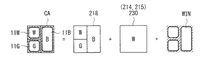
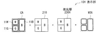
図2は、表示部10におけるサブ画素11の配置の一例を模式的に表すものである。図2において、網掛け部分は、4つのサブ画素11R,11G,11B,11Wの開口部WINを表している。表示部10には、3つのサブ画素11W,11G,11Bにより構成されるセルCAと、3つのサブ画素11W,11G,11Rにより構成されるセルCBが並設されている。すなわち、セルCAは、4色のサブ画素11のうちの赤色のサブ画素11Rを省いたものであり、セルCBは、4色のサブ画素11のうちの青色のサブ画素11Bを省いたものである。セルCAにおいて、この例では、白色(W)のサブ画素11Wは左上に配置され、緑色(G)のサブ画素11Gは左下に配置され、青色(B)のサブ画素11Bは右側に配置されている。同様に、セルCBにおいて、この例では、白色(W)のサブ画素11Wは左上に配置され、緑色(G)のサブ画素11Gは左下に配置され、赤色(R)のサブ画素11Rは右側に配置されている。これにより、表示部10では、サブ画素11R,11Bが、サブ画素11W,11Gよりも少なく形成されるとともに、サブ画素11R,11Bの開口部WINが、サブ画素11W,11Gの開口部WINよりも大きく形成されるようになっている。
FIG. 2 schematically illustrates an example of the arrangement of the sub-pixels 11 in the
図2に示すように、セルCAおよびセルCBは、列方向(垂直方向)に交互に配置されるとともに、行方向(水平方向)に交互に配置されている。これにより、白色のサブ画素11Wおよび緑色のサブ画素11Gは、列方向において交互に配置される。そして、赤色のサブ画素11Rおよび青色のサブ画素11Bは、列方向において交互に配置されるとともに、行方向において交互に配置される。すなわち、表示部10におけるサブ画素11Rの配置パターンおよびサブ画素11Bの配置パターンは、それぞれ市松模様を構成するようになっている。
As shown in FIG. 2, the cells CA and CB are alternately arranged in the column direction (vertical direction) and alternately in the row direction (horizontal direction). As a result, the white sub-pixels 11W and the
図3は、表示部10の回路構成の一例を表すものである。表示部10は、行方向に延伸する複数の走査線WSLおよび複数の電源線PLと、列方向に延伸する複数のデータ線DTLとを有している。データ線DTLの一端はデータ線駆動部27に接続されている。また、図示していないが、走査線WSLの一端は走査線駆動部23に接続され、電源線PLの一端は電源線駆動部26に接続されている。各サブ画素11は、走査線WSLとデータ線DTLとの交差部に配置されている。1つのセルCAに属するサブ画素11W,11G,11Bは、同じ走査線WSおよび同じ電源線PLに接続されるとともに、互いに異なるデータ線DTLに接続されている。同様に、1つのセルCBに属するサブ画素11W,11G,11Rは、同じ走査線WSおよび同じ電源線PLに接続されるとともに、互いに異なるデータ線DTLに接続されている。
FIG. 3 illustrates an example of a circuit configuration of the
図4は、サブ画素11の回路構成の一例を表すものである。サブ画素11は、書込トランジスタWSTrと、駆動トランジスタDRTrと、発光素子19と、容量素子Csとを備えている。すなわち、この例では、サブ画素11は、2つのトランジスタ(書込トランジスタWSTr、駆動トランジスタDRTr)および1つの容量素子Csを用いて構成される、いわゆる「2Tr1C」の構成を有するものである。
FIG. 4 illustrates an example of a circuit configuration of the sub-pixel 11. The sub-pixel 11 includes a write transistor WSTr, a drive transistor DRTr, a
書込トランジスタWSTrおよび駆動トランジスタDRTrは、例えば、NチャネルMOS(Metal Oxide Semiconductor)型のTFT(Thin Film Transistor;薄膜トランジスタ)により構成されるものである。書込トランジスタWSTrは、ゲートが走査線WSLに接続され、ソースがデータ線DTLに接続され、ドレインが駆動トランジスタDRTrのゲートおよび容量素子Csの一端に接続されている。駆動トランジスタDRTrは、ゲートが書込トランジスタWSTrのドレインおよび容量素子Csの一端に接続され、ドレインが電源線PLに接続され、ソースが容量素子Csの他端および発光素子19のアノードに接続されている。
The write transistor WSTr and the drive transistor DRTr are configured by, for example, an N-channel MOS (Metal Oxide Semiconductor) TFT (Thin Film Transistor). The write transistor WSTr has a gate connected to the scanning line WSL, a source connected to the data line DTL, and a drain connected to the gate of the drive transistor DRTr and one end of the capacitive element Cs. The drive transistor DRTr has a gate connected to the drain of the write transistor WSTr and one end of the capacitive element Cs, a drain connected to the power supply line PL, and a source connected to the other end of the capacitive element Cs and the anode of the
容量素子Csは、一端が駆動トランジスタDRTrのゲート等に接続され、他端は駆動トランジスタDRTrのソース等に接続されている。発光素子19は、有機EL素子を用いて構成された発光素子であり、アノードが駆動トランジスタDRTrのソースおよび容量素子Csの他端に接続され、カソードには、駆動部20によりカソード電圧Vcathが供給されている。
One end of the capacitive element Cs is connected to the gate of the driving transistor DRTr and the other end is connected to the source and the like of the driving transistor DRTr. The
図5は、表示部10の断面図を表すものである。表示部10は、透明基板200と、ゲート201と、ポリシリコン203と、アノード212と、発光層230と、カソード216と、カラーフィルタ218とを有している。
FIG. 5 illustrates a cross-sectional view of the
透明基板200は、表示部10の支持基板であり、例えば、ガラスやプラスチックなどにより構成されている。透明基板200上には、ゲート201が形成されている。このゲート201は、例えばモリブデン(Mo)などにより構成される。透明基板200およびゲート201の上には絶縁層202が形成されている。この絶縁層202は、例えば、酸化シリコン(SiO2)や、窒化シリコン(SiNx)などにより構成される。この絶縁層202の上には、ゲート201に対応する領域にポリシリコン203が形成されている。ゲート201およびポリシリコン203は、駆動トランジスタDRTrなどを構成するものである。なお、この例では、ゲート201の上部にポリシリコン203を形成する、いわゆるボトムゲート構造によりトランジスタを構成したが、これに限定されるものではなく、ゲートの下部にポリシリコンを形成する、いわゆるトップゲート構造によりトランジスタを構成してもよい。ポリシリコン203および絶縁層202の上には、絶縁層204が形成されている。この絶縁層204は、例えば絶縁層202と同様の材料により構成される。また、ポリシリコン203が形成された領域の一部には、絶縁層204を貫通するように、コンタクト/配線205が形成されている。配線205は、例えば、チタン(Ti)/アルミニウム(Al)/チタン(Ti)の3層により構成することができる。
The
絶縁層204の上には、絶縁層211が形成されている。絶縁層211は、例えば、ポリイミドやアクリル樹脂などにより構成される。絶縁層211の上には、アノード212が形成されている。アノード212は、絶縁層211を貫通して、駆動トランジスタDRTrのソースに係るコンタクト/配線205と接続されている。アノード212は、例えば、ITO/Al合金、Al合金、ITO/Ag、ITO/Ag合金などにより構成されている。すなわち、アノード212は、光を反射する性質を有することが望ましい。アノード212および絶縁層211の上には、絶縁層213が形成されている。絶縁層213は、例えば絶縁層211と同様の材料により構成される。この絶縁層213には、アノード212が形成された領域の一部に開口部WINが設けられている。アノード212および絶縁層213の上部には、黄色発光層214および青色発光層215からなる発光層230が一様に形成されている。黄色発光層214は、黄色(Y)の光を発する有機EL層であり、青色発光層215は、青色(B)の光を発する有機EL層である。この黄色発光層214は、黄色に光る材料により構成してもよいし、または、緑色(G)に光る材料に赤色(R)に光る材料をドープして構成してもよい。青色発光層215は、例えば、青色に光る材料により構成することができる。青色発光層215の上には、カソード216が一様に形成されている。カソード216は、透明または半透明の電極であり、例えば、マグネシウム銀(MgAg)や、IZO(登録商標)により構成することができる。マグネシウム銀で構成した場合には、膜厚を例えば数nm程度にすることにより半透明にすることができる。IZOで構成した場合には、例えば数十nm〜数千nmの膜厚で形成することが望ましい。すなわち、IZOは透明な材料であるため、所望の低いシート抵抗値を実現できるようにやや厚く形成することができる。カソード216の上には、この例では絶縁層217が形成されている。絶縁層217は、例えば窒化シリコン(SiNx)などにより構成される。絶縁層217は、発光層230に水分が侵入し、発光効率などの特性が変化するのを防止するために設けられるものである。なお、この水分の侵入に起因する諸問題が他の技術により解決できる場合、この絶縁層217を省いてもよい。この絶縁層217には、封止用の樹脂である絶縁層221を介して、カラーフィルタ218やブラックマトリクス219が表面に形成された透明基板220が貼り合わせられている。赤色(R)のカラーフィルタ218は、サブ画素11Rに対応する部分に配置され、緑色(G)のカラーフィルタ218はサブ画素11Gに対応する部分に配置され、青色(B)のカラーフィルタ218はサブ画素11Bに対応する部分に配置され、白色(W)のカラーフィルタ218はサブ画素11Wに対応する部分に配置されている。
An insulating
この構成により、黄色発光層214から射出した黄色の光と、青色発光層215から射出した青色の光は、混ざり合って白色光となり、支持基板である透明基板200とは反対の方向に進む。すなわち、発光素子19は、いわゆるトップエミッション型の発光素子である。そして、この白色光は、カラーフィルタ218を介して表示面より出力される。具体的には、サブ画素11R,11G,11Bでは、赤色(R)、緑色(G)、青色(B)のカラーフィルタ218により、白色光から赤色成分、緑色成分、青色成分がそれぞれ分離され出力される。また、サブ画素11Wでは、白色(W)のカラーフィルタ218により白色光の色域が調整される。なお、画質(色域)に対する要求がさほど高くないアプリケーションなどにおいては、白色(W)のカラーフィルタ218を設けなくてもよい。
With this configuration, the yellow light emitted from the yellow light-emitting
図6Aは、セルCAにおける3つのサブ画素11の構成を模式的に表すものであり、図6Bは、セルCBにおける3つのサブ画素11の構成を模式的に表すものである。セルCAにおける3つのサブ画素11W,11G,11Bでは、図6Aに示すように、発光層230(黄色発光層214および青色発光層215)の開口部WINから射出した白色(W)の光が、白色(W)、緑色(G)、および青色(B)のカラーフィルタ218をそれぞれ通過する。同様に、セルCBにおける3つのサブ画素11W,11G,11Rでは、図6Bに示すように、発光層230の開口部WINから射出した白色(W)の光が、白色(W)、緑色(G)、および赤色(R)のカラーフィルタ218をそれぞれ通過するようになっている。
6A schematically illustrates the configuration of the three
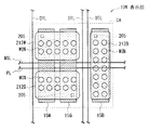
図7は、セルCAにおけるアノード212の配置を表すものである。セルCAには、3つの回路領域15W,15G,15Bと、3つのアノード212W,212G,212Bが設けられている。
FIG. 7 shows the arrangement of the
回路領域15Wは、サブ画素11Wにおける発光素子19以外の素子(書込トランジスタWSTr、駆動トランジスタDRTr、および容量素子Cs)が配置される領域である。同様に、回路領域15Gは、サブ画素11Gにおける発光素子19以外の素子が配置される領域であり、回路領域15Bは、サブ画素11Bにおける発光素子19以外の素子が配置される領域である。これらの回路領域15W,15G,15Bには、書込トランジスタWSTr、駆動トランジスタDRTr、および容量素子Csが同じようにレイアウトされている。この例では、回路領域15Gのレイアウトは、回路領域15W,15Bのレイアウトを180度回転し、走査線WSLおよび電源線PLとの接続部分を修正したものである。なお、回路領域15Gのレイアウトは、回路領域15W,15Bのレイアウトを上下反転し、これらの配線との接続部分を修正したものであってもよいし、全く異なる別のレイアウトであってもよい。このように、同じレイアウトを回転または反転して流用することにより、レイアウト作業の効率を高めることができる。この例では、3つの回路領域15W,15G,15Bは、セルCAにおいて、データ線DTLの延伸方向(列方向)に延伸するとともに、データ線DTLの延伸方向と直交する方向(行方向)に並設されている。具体的には、この例では、セルCAにおいて、1本のデータ線DTL、回路領域15W、回路領域15G、2本のデータ線DTL、および回路領域15Bが、左から右へこの順に配置されている。このように、回路領域15を列方向に延伸するように設けることにより、例えば、駆動トランジスタDRTrのチャネル長(L)を長くすることができ、これにより、サブ画素11の特性ばらつきを抑えることができるようになっている。
The
アノード212Wはサブ画素11Wのアノード212であり、アノード212Gはサブ画素11Gのアノード212であり、アノード212Bはサブ画素11Bのアノード212である。これらのアノード212W,212G,212Bは、回路領域15W,15G,15Bに形成された駆動トランジスタDRTrのソースと、それぞれコンタクト205を介して接続されている。セルCAにおいて、アノード212Wは左上に配置され、アノード212Gは左下に配置され、アノード212Bは右側に配置されている。これらのアノード212W,212G,212Bは、データ線DTLと重ならないように配置されている。そして、アノード212W,212G,212B上の開口部WINにおいて、発光層230が白色光を発光するようになっている。
The
以上、セルCAについて説明したが、セルCBについても同様である。すなわち、セルCBには、3つの回路領域15W,15G,15Rと、3つのアノード212W,212G,212Rが設けられている。回路領域15Rは、サブ画素11Rにおける発光素子19以外の素子が配置される領域であり、アノード212Rは、サブ画素11Rのアノード212である。セルCBにおいて、1本のデータ線DTL、回路領域15W、回路領域15G、2本のデータ線DTL、および回路領域15Rが、左から右へこの順に配置されている。また、セルCBにおいて、アノード212Wは左上に配置され、アノード212Gは左下に配置され、アノード212Rは右側に配置されている。これらのアノード212W,212G,212Rは、データ線DTLと重ならないように配置されている。
Although the cell CA has been described above, the same applies to the cell CB. That is, the cell CB is provided with three
図1において、映像信号処理部30は、外部から供給される映像信号Sdispに対して、RGBW変換やガンマ変換などを行い、映像信号Sdisp2を生成するものである。映像信号Sdispは、赤色(R)、緑色(G)、および青色(B)の輝度情報Iを有するRGB信号である。
In FIG. 1, a video
図8は、映像信号処理部30の一構成例を表すものである。映像信号処理部30は、リニアガンマ変換部31と、RGBW変換部32と、フィルタ処理部33R,33Bと、輝度情報抽出部34R,34Bと、信号処理部35と、パネルガンマ変換部36とを有している。
FIG. 8 illustrates a configuration example of the video
リニアガンマ変換部31は、入力された映像信号Sdispを、線形なガンマ特性を有する映像信号S31に変換するものである。すなわち、外部から供給される映像信号は、一般的な表示装置の特性を考慮した非線形なガンマ特性を有している。よって、このリニアガンマ変換部31は、RGBW変換部32や信号処理部35などにおける処理を容易にするため、このような非線形なガンマ特性を線形なガンマ特性に変換する。ガンマ変換部31は、例えばルックアップテーブルを有しており、このルックアップテーブルを用いてこのようなガンマ変換を行うようになっている。
The
RGBW変換部32は、映像信号S31に対してRGBW変換を行うものである。具体的には、RGBW変換部32は、赤色、緑色、および青色の輝度情報Iを有するRGB信号を、赤色(R)、緑色(G)、青色(B)、および白色(W)の輝度情報Iを有するRGBW信号に変換する。そして、RGBW変換部32は、赤色(R)の輝度情報Iを信号SR32として出力し、緑色(G)の輝度情報Iを信号SG32として出力し、青色(B)の輝度情報Iを信号SB32として出力し、白色(W)の輝度情報Iを信号SW32として出力するようになっている。
The
フィルタ処理部33Rは、信号SR32に対してフィルタ処理を行うものである。このフィルタ処理部33Rは、この例では、低域通過フィルタとして機能するFIR(Finite impulse response)フィルタにより構成されるものである。フィルタ処理部33Rは、入力された信号SR32に基づいて、赤色(R)の輝度情報Iのマップを作成し、そのマップに対してフィルタ処理を行う。そして、フィルタ処理部33Rは、フィルタ処理を行った輝度情報Iを信号SR33として出力するようになっている。 The filter processing unit 33R performs filter processing on the signal SR32. In this example, the filter processing unit 33R is configured by an FIR (Finite impulse response) filter that functions as a low-pass filter. The filter processing unit 33R creates a map of red (R) luminance information I based on the input signal SR32, and performs filter processing on the map. The filter processing unit 33R outputs the luminance information I subjected to the filter processing as a signal SR33.
フィルタ処理部33Bは、信号SB32に対してフィルタ処理を行うものである。このフィルタ処理部33Bは、フィルタ処理部33Rと同様に、低域通過フィルタとして機能するFIRフィルタにより構成されるものである。フィルタ処理部33Bは、入力された信号SB32に基づいて、青色(B)の輝度情報Iのマップを作成し、そのマップに対してフィルタ処理を行う。そして、フィルタ処理部33Bは、フィルタ処理を行った輝度情報Iを信号SB33として出力するようになっている。
The
輝度情報抽出部34Rは、信号SR33に含まれる赤色(R)の輝度情報Iから、表示部10に表示する輝度情報Iを抽出するものである。
The luminance
輝度情報抽出部34Bは、信号SB33に含まれる青色(B)の輝度情報Iから、表示部10に表示する輝度情報Iを抽出するものである。
The luminance
図9Aは、輝度情報抽出部34Rの一動作例を表すものであり、図9Bは、輝度情報抽出部34Bの一動作例を表すものである。輝度情報抽出部34Rは、信号SR33に基づいて、赤色(R)の輝度情報IのマップMAPRを生成する。そして、輝度情報抽出部34Rは、図9Aに示すように、そのマップMAPRから、表示部10における赤色のサブ画素11Rの配置パターン(図2)に応じた座標における輝度情報I(図9Aにおける斜線部)を抽出する。すなわち、輝度情報抽出部34Rは、抽出パターンが市松模様になるように、輝度情報Iを抽出する。そして、輝度情報抽出部34Rは、抽出した輝度情報Iを、信号SR34として出力するようになっている。同様に、輝度情報抽出部34Bは、信号SB33に基づいて、青色(B)の輝度情報IのマップMAPBを生成し、そのマップMAPBから、表示部10における青色のサブ画素11Bの配置パターン(図2)に応じた座標における輝度情報I(図9Bにおける斜線部)を抽出する。そして、輝度情報抽出部34Bは、抽出した輝度情報Iを、信号SB34として出力するようになっている。
FIG. 9A illustrates an operation example of the luminance
このように、映像信号処理部30では、フィルタ処理部33R,33Bが輝度情報Iに対してフィルタ処理を行う。輝度情報抽出部34R,34Bは、そのフィルタ処理を行った輝度情報Iから、表示部10に表示する輝度情報Iを抽出している。これにより、表示装置1では、赤色および青色の成分に対してのみ、画像の解像度(エッジの尖鋭度)を下げるとともに、抽出された赤色および青色の輝度情報Iが、表示部10におけるサブ画素11R,11Bの位置を反映するようになっている。
As described above, in the video
信号処理部35は、信号SW32,SG32,SR34,SB34からなる映像信号S34に対して所定の信号処理を行い、その結果を映像信号S35として出力するものである。所定の信号処理としては、例えば、映像信号S34により表現される色域および色温度を、表示部10の色域および色温度に変換する、いわゆる色域変換などが挙げられる。
The
パネルガンマ変換部36は、線形なガンマ特性を有する映像信号S35を、表示部10の特性に対応した非線形なガンマ特性を有する映像信号S36に変換(パネルガンマ変換)するものである。このパネルガンマ変換部36は、リニアガンマ変換部31と同様に、例えばルックアップテーブルを有しており、このルックアップテーブルを用いてこのようなガンマ変換を行うようになっている。
The panel
図1において、タイミング生成部22は、外部から供給される同期信号Ssyncに基づいて、走査線駆動部23、電源線駆動部26、およびデータ線駆動部27に対してそれぞれ制御信号を供給し、これらがお互いに同期して動作するように制御する回路である。
In FIG. 1, the
走査線駆動部23は、タイミング生成部22から供給された制御信号に従って、複数の走査線WSLに対して走査信号WSを順次印加することにより、サブ画素11を順次選択するものである。
The scanning
電源線駆動部26は、タイミング生成部22から供給された制御信号に従って、複数の電源線PLに対して電源信号DSを順次印加することにより、サブ画素11の発光動作および消光動作の制御を行うものである。電源信号DSは、電圧Vccpと電圧Viniとの間で遷移するものである。後述するように、電圧Viniは、サブ画素11を初期化するための電圧であり、電圧Vccpは、駆動トランジスタDRTrに電流を流して発光素子19を発光させるための電圧である。
The power supply
データ線駆動部27は、映像信号処理部30から供給された映像信号Sdisp2およびタイミング生成部22から供給された制御信号に従って、各サブ画素11の発光輝度を指示する画素電圧Vsig、および後述するVth補正を行うための電圧Vofsを含む信号Sigを生成し、各データ線DTLに印加するものである。
The data
この構成により、駆動部20は、後述するように、サブ画素11に対して駆動トランジスタDRTrの素子ばらつきが画質に与える影響を抑えるための補正(Vth補正およびμ(移動度)補正)を行い、サブ画素11に対して画素電圧Vsigの書込みを行う。そして、その後に、サブ画素11の発光素子19が、書き込まれた画素電圧Vsigに応じた輝度で発光するようになっている。
With this configuration, as will be described later, the
ここで、サブ画素11Gは、本開示における「第1の画素」の一具体例に対応し、サブ画素11Bは、本開示における「第2の画素」の一具体例に対応し、サブ画素11Rは、本開示における「第3の画素」の一具体例に対応する。サブ画素11Wは、本開示における「非基本色画素」の一具体例に対応する。セルCAを構成するサブ画素11G,11W,11Bは、本開示における「第1の画素セット」の一具体例に対応する。セルCBを構成するサブ画素11G,11W,11Rは、本開示における「第2の画素セット」の一具体例に対応する。セルCAは、本開示における「第1の画素セル」の一具体例に対応する。セルCBは、本開示における「第2の画素セル」の一具体例に対応する。データ線DTLは、本開示における「信号線」の一具体例に対応する。信号Sigは、本開示における「画素信号」の一具体例に対応する。駆動トランジスタDRTrは、本開示における「トランジスタ」の一具体例に対応する。
Here, the
[動作および作用]
続いて、本実施の形態の表示装置1の動作および作用について説明する。
[Operation and Action]
Subsequently, the operation and action of the
(全体動作概要)
まず、図1を参照して、表示装置1の全体動作概要を説明する。映像信号処理部30は、外部から供給される映像信号Sdispに対してRGBW変換やガンマ変換などを行い、映像信号Sdisp2を生成する。タイミング生成部22は、外部から供給される同期信号Ssyncに基づいて、走査線駆動部23、電源線駆動部26およびデータ線駆動部27に対してそれぞれ制御信号を供給し、これらがお互いに同期して動作するように制御する。走査線駆動部23は、タイミング生成部22から供給された制御信号に従って、複数の走査線WSLに対して走査信号WSを順次印加することにより、サブ画素11を順次選択する。電源線駆動部26は、タイミング生成部22から供給された制御信号に従って、複数の電源線PLに対して電源信号DSを順次印加することにより、サブ画素11の発光動作および消光動作の制御を行う。データ線駆動部27は、映像信号処理部30から供給された映像信号Sdisp2およびタイミング生成部22から供給された制御信号に従って、各サブ画素11の輝度に対応する画素電圧Vsig、およびVth補正を行うための電圧Vofsを含む信号Sigを生成し、各データ線DTLに印加する。表示部10は、駆動部20から供給された走査信号WS、電源信号DS、および信号Sigに基づいて表示を行う。
(Overview of overall operation)
First, an overall operation overview of the
(詳細動作)
次に、表示装置1の詳細動作を説明する。
(Detailed operation)
Next, the detailed operation of the
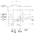
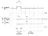
図10は、表示装置1における表示動作のタイミング図を表すものである。この図は、着目した1つのサブ画素11に対する表示駆動の動作例を表すものである。図10において、(A)は走査信号WSの波形を示し、(B)は電源信号DSの波形を示し、(C)は信号Sigの波形を示し、(D)は駆動トランジスタDRTrのゲート電圧Vgの波形を示し、(E)は駆動トランジスタDRTrのソース電圧Vsの波形を示す。
FIG. 10 shows a timing chart of the display operation in the
駆動部20は、1水平期間(1H)内において、サブ画素11の初期化を行い(初期化期間P1)、駆動トランジスタDRTrの素子ばらつきが画質に与える影響を抑えるためのVth補正を行い(Vth補正期間P2)、サブ画素11に対して画素電圧Vsigの書込みを行うとともに、Vth補正とは異なるμ(移動度)補正を行う(書込・μ補正期間P3)。そして、その後に、サブ画素11の発光素子19が、書き込まれた画素電圧Vsigに応じた輝度で発光する(発光期間P4)。以下に、その詳細を説明する。
The
まず、電源線駆動部26は、初期化期間P1に先立つタイミングt1において、電源信号DSを電圧Vccpから電圧Viniに変化させる(図10(B))。これにより、駆動トランジスタDRTrがオン状態になり、駆動トランジスタDRTrのソース電圧Vsが、電圧Viniに設定される(図10(E))。
First, the power supply
次に、駆動部20は、タイミングt2〜t3の期間(初期化期間P1)において、サブ画素11を初期化する。具体的には、タイミングt2において、データ線駆動部27が、信号Sigを電圧Vofsに設定し(図10(C))、走査線駆動部23が、走査信号WSの電圧を低レベルから高レベルに変化させる(図10(A))。これにより、書込トランジスタWSTrがオン状態になり、駆動トランジスタDRTrのゲート電圧Vgが電圧Vofsに設定される(図10(D))。このようにして、駆動トランジスタDRTrのゲート・ソース間電圧Vgs(=Vofs−Vini)は、駆動トランジスタDRTrの閾値電圧Vthよりも大きい電圧に設定され、サブ画素11が初期化される。
Next, the
次に、駆動部20は、タイミングt3〜t4の期間(Vth補正期間P2)において、Vth補正を行う。具体的には、電源線駆動部26が、タイミングt3において、電源信号DSを電圧Viniから電圧Vccpに変化させる(図10(B))。これにより、駆動トランジスタDRTrは飽和領域で動作するようになり、ドレインからソースに電流Idsが流れ、ソース電圧Vsが上昇する(図10(E))。その際、この例では、ソース電圧Vsは発光素子19のカソードの電圧Vcathよりも低いため、発光素子19は逆バイアス状態を維持し、発光素子19には電流は流れない。このようにソース電圧Vsが上昇することにより、ゲート・ソース間電圧Vgsが低下するため、電流Idsは低下する。この負帰還動作により、電流Idsは“0”(ゼロ)に向かって収束していく。言い換えれば、駆動トランジスタDRTrのゲート・ソース間電圧Vgsは、駆動トランジスタDRTrの閾値電圧Vthと等しくなる(Vgs=Vth)ように収束していく。
Next, the
次に、走査線駆動部23は、タイミングt4において、走査信号WSの電圧を高レベルから低レベルに変化させる(図10(A))。これにより、書込トランジスタWSTrはオフ状態になる。そして、データ線駆動部27は、タイミングt5において、信号Sigを画素電圧Vsigに設定する(図10(C))。
Next, the scanning
次に、駆動部20は、タイミングt6〜t7の期間(書込・μ補正期間P3)において、サブ画素11に対して画素電圧Vsigの書込みを行うとともにμ補正を行う。具体的には、走査線駆動部23が、タイミングt6において、走査信号WSの電圧を低レベルから高レベルに変化させる(図10(A))。これにより、書込トランジスタWSTrはオン状態になり、駆動トランジスタDRTrのゲート電圧Vgが、電圧Vofsから画素電圧Vsigに上昇する(図10(D))。このとき、駆動トランジスタDRTrのゲート・ソース間電圧Vgsが閾値電圧Vthより大きくなり(Vgs>Vth)、ドレインからソースへ電流Idsが流れるため、駆動トランジスタDRTrのソース電圧Vsが上昇する(図10(E))。このような負帰還動作により、駆動トランジスタDRTrの素子ばらつきの影響が抑えられ(μ補正)、駆動トランジスタDRTrのゲート・ソース間電圧Vgsは、画素電圧Vsigに応じた電圧Vemiに設定される。なお、このようなμ補正の方法については、例えば、特開2006−215213に記載がある。
Next, the
次に、駆動部20は、タイミングt7以降の期間(発光期間P4)において、サブ画素11を発光させる。具体的には、タイミングt7において、走査線駆動部23は、走査信号WSの電圧を高レベルから低レベルに変化させる(図10(A))。これにより、書込トランジスタWSTrがオフ状態になり、駆動トランジスタDRTrのゲートがフローティングとなるため、これ以後、容量素子Csの端子間電圧、すなわち、駆動トランジスタDRTrのゲート・ソース間電圧Vgsは維持される。そして、駆動トランジスタDRTrに電流Idsが流れるにつれ、駆動トランジスタDRTrのソース電圧Vsが上昇し(図10(E))、これに伴って駆動トランジスタDRTrのゲート電圧Vgも上昇する(図10(D))。そして、駆動トランジスタDRTrのソース電圧Vsが、発光素子19の閾値電圧Velと電圧Vcathの和(Vel+Vcath)よりも大きくなると、発光素子19のアノード・カソード間に電流が流れ、発光素子19が発光する。すなわち、発光素子19の素子ばらつきに応じた分だけソース電圧Vsが上昇し、発光素子19が発光する。
Next, the
その後、表示装置1では、所定の期間(1フレーム期間)が経過したのち、発光期間P4から書込期間P1に移行する。駆動部20は、この一連の動作を繰り返すように表示部10を駆動する。
Thereafter, in the
(画質および消費電力について)
表示装置1は、消費電力を低減するために、いくつかの工夫がなされている。以下に、いくつかの比較例を挙げて、それらの技術について詳細に説明する。
(Image quality and power consumption)
The
(比較例1)
表示装置1では、図2に示したように、4色のサブ画素のうち、赤色(R)のサブ画素を省いてセルCAを構成するとともに、青色(B)のサブ画素を省いてセルCBを構成したので、以下に説明する表示装置1Rと比べて、画質の低下を抑えつつ、消費電力を低減することができる。
(Comparative Example 1)
In the
図11は、比較例1に係る表示装置1Rにおける表示部10Rの一構成例を表すものである。表示部10Rには、複数の画素Pixがマトリクス状に配置されている。各画素Pixは、赤色(R)、緑色(G)、青色(B)、白色(W)の4つのサブ画素12(12R,12G,12B,12W)を有している。この例では、これらの4つのサブ画素12R,12G,12B,12Wは、画素Pixにおいて2行2列で配置されている。具体的には、画素Pixにおいて、左上に赤色(R)のサブ画素12Rを配置し、右上に緑色(G)のサブ画素12Gを配置し、左下に白色(W)のサブ画素12Wを配置し、右下に青色(B)のサブ画素12Bを配置している。
FIG. 11 illustrates a configuration example of the display unit 10R in the display device 1R according to the first comparative example. In the display unit 10R, a plurality of pixels Pix are arranged in a matrix. Each pixel Pix has four sub-pixels 12 (12R, 12G, 12B, 12W) of red (R), green (G), blue (B), and white (W). In this example, these four
ここで、比較例1に係る画素Pix(図11)は、本実施の形態におけるセルCAまたはセルCB(図2)に対応するものである。具体的には、本実施の形態におけるセルCAは、比較例1に係る画素Pixから赤色のサブ画素12Rを省いたものに対応しており、本実施の形態におけるセルCBは、比較例1に係る画素Pixから青色のサブ画素12Bを省いたものに対応している。
Here, the pixel Pix (FIG. 11) according to the comparative example 1 corresponds to the cell CA or the cell CB (FIG. 2) in the present embodiment. Specifically, the cell CA in the present embodiment corresponds to the pixel Pix according to the comparative example 1 in which the
図12は、比較例1に係る表示部10Rの回路構成の一例を表すものである。表示部10Rでは、1つの画素Pixに属するサブ画素12Rとサブ画素12Gは、同じ走査線WS(例えばk番目の走査線WS(k))および同じ電源線PL(例えばk番目の電源線PL(k))に接続されている。また、その画素Pixに属するサブ画素12Wとサブ画素12Bは、同じ走査線WS(例えば(k+1)番目の走査線WS(k+1))および同じ電源線PL(例えば(k+1)番目の電源線PL(k+1))に接続されている。 FIG. 12 illustrates an example of a circuit configuration of the display unit 10R according to the first comparative example. In the display unit 10R, the sub-pixel 12R and the sub-pixel 12G belonging to one pixel Pix have the same scanning line WS (for example, the k-th scanning line WS (k)) and the same power line PL (for example, the k-th power line PL ( k)). Further, the sub-pixel 12W and the sub-pixel 12B belonging to the pixel Pix have the same scanning line WS (for example, the (k + 1) th scanning line WS (k + 1)) and the same power line PL (for example, the (k + 1) th power line PL ( k + 1)).
また、1つの画素Pixに属するサブ画素12Rとサブ画素12Wは、同じデータ線DTL(例えばj番目のデータ線DTL(j))に接続され、その画素Pixに属するサブ画素12Gとサブ画素12Bは、同じデータ線DTL(例えば(j+1)番目のデータ線DTL(j+1))に接続されている。 Further, the sub-pixel 12R and the sub-pixel 12W belonging to one pixel Pix are connected to the same data line DTL (for example, the j-th data line DTL (j)), and the sub-pixel 12G and the sub-pixel 12B belonging to the pixel Pix are Are connected to the same data line DTL (for example, (j + 1) th data line DTL (j + 1)).
比較例1に係る表示装置1Rでは、走査駆動を行う際、1つの画素Pixを構成する4つのサブ画素12のうちの、サブ画素12R,12Gと、サブ画素12B,12Wとを、異なる期間において駆動する必要がある。具体的には、例えば、1水平期間の前半においてサブ画素12R,12Gを駆動し、1水平期間の後半においてサブ画素12B,12Wを駆動する必要がある。よって、データ線駆動部27Rは、例えば1フレーム期間において、より多くのサブ画素12に、画素電圧Vsigを供給する必要がある。すなわち、データ線DTLを駆動する際の駆動周波数が高くなってしまう。これにより、消費電力が高くなるおそれがある。
In the display device 1R according to the comparative example 1, when performing the scanning drive, the sub-pixels 12R and 12G and the sub-pixels 12B and 12W among the four sub-pixels 12 constituting one pixel Pix are set in different periods. Need to drive. Specifically, for example, it is necessary to drive the
また、比較例1に係る表示装置1Rでは、1つの画素Pixにつき6本の配線(2本の走査線WS、2本の電源線PL、および2本のデータ線DTL)が必要となる。よって、表示装置1Rでは、これらの配線を駆動するための電力を要するため、消費電力が高くなるおそれがある。 Further, in the display device 1R according to the comparative example 1, six wirings (two scanning lines WS, two power supply lines PL, and two data lines DTL) are required for one pixel Pix. Therefore, the display device 1R requires power for driving these wirings, which may increase power consumption.
また、比較例1に係る表示装置1Rでは、1つの画素Pixが4つのサブ画素12を有するようにしたので、表示部10Rにおけるサブ画素12の数が多くなる。これにより、各サブ画素12の面積が小さくなるため、開口率が低下してしまう。すなわち、例えば、アノード間隔などのデザインルールにより、アノードの大きさは制限され、またアノードの縁と開口部WINの縁との間の距離に関するデザインルールにより開口部WINの大きさも制限されるため、開口部WINを大きくすることができず、開口率が低下してしまう。このように開口率が低い場合には、開口率が高い場合に比べて、同じ発光輝度を実現するための発光層230の電流密度が高くなってしまい、画質が劣化するおそれがある。すなわち、発光層230を構成する有機EL層は、一般に、電流密度が高いほど経時劣化(いわゆる焼き付き)が生じやすいため、電流密度が高くなることにより、画質が低下するおそれがある。
Further, in the display device 1R according to the comparative example 1, since one pixel Pix includes the four
また、比較例1に係る表示装置1Rでは、上述したように駆動周波数が高くなってしまうため、例えば、サブ画素12に画素電圧Vsigを書き込むための十分な時間が確保しにくくなり、画質が低下するおそれがある。 Further, in the display device 1R according to the comparative example 1, since the driving frequency becomes high as described above, for example, it is difficult to secure a sufficient time for writing the pixel voltage Vsig to the sub-pixel 12, and the image quality is deteriorated. There is a risk.
一方、本実施の形態に係る表示装置1では、図2,3に示したように、赤色のサブ画素11Rを省いてセルCAを構成して、1つのセルCAに属する3つのサブ画素11W,11G,11Bが同じ走査線WSL等に接続されるようにするとともに、青色のサブ画素11Bを省いてセルCBを構成し、1つのセルCBに属する3つのサブ画素11W,11G,11Rが同じ走査線WSL等に接続されるようにしている。これにより、1水平期間において、セルCAに属する3つのサブ画素11W,11G,11Bをまとめて駆動することができ、同様に、1水平期間において、セルCBに属する3つのサブ画素11W,11G,11Rをまとめて駆動することができる。よって、データ線駆動部27は、例えば、1フレーム期間において、比較例1の場合の半分の数のサブ画素11に、画素電圧Vsigを供給すればよい。すなわち、表示装置1では、データ線DTLを駆動する際の駆動周波数を低くすることができるため、消費電力を低減することができる。
On the other hand, in the
また、本実施の形態に係る表示装置1では、セルCA,CBのそれぞれにつき5本の配線(1本の走査線WS、1本の電源線PL、および3本のデータ線DTL)が必要となる。すなわち、比較例1の場合(6本)に比べて少ない配線で済む。よって、これらの配線に対する駆動電力が少なくて済むため、消費電力を低減することができる。
Further, in
また、本実施の形態に係る表示装置1では、赤色のサブ画素11Rを省いてセルCAを構成し、青色のサブ画素11Bを省いてセルCBを構成することにより、画質の低下を抑えつつ、消費電力を低減することができる。すなわち、表示装置1では、上述したように、消費電力を低減するために、赤色のサブ画素11Rや青色のサブ画素11Bを少なくしているため、白色(W)のサブ画素11Wや緑色(G)のサブ画素11Gの解像度に比べて、赤色(R)のサブ画素11Rや青色(B)のサブ画素11Bの解像度が低下している。しかしながら、人間は、赤色(R)と青色(B)などのいわゆる色度成分の解像度が低下しても、画質の低下を感じないことが知られている。すなわち、色を輝度成分と色度成分に分けた場合、人間は、輝度成分の解像度を下げると画質が低下したように感じるが、色度成分の解像度を下げても、さほど画質の低下を感じない。サブ画素11が発光する4色(赤色、緑色、青色、白色)のうち、白色(W)と緑色(G)は輝度成分への寄与が多く、一方、赤色(R)と青色(B)は輝度成分への寄与が少ない。表示装置1では、このように、輝度成分への寄与が少ない赤色のサブ画素11Rや青色のサブ画素11Bを少なくしたので、画質の低下を抑えつつ、消費電力を低減することができる。
Further, in the
また、本実施の形態に係る表示装置1では、サブ画素11の数を減らしたので、各サブ画素11を大きくすることができ、サブ画素11R,11Bの開口率を高くすることができる。これにより、発光層の経時劣化(いわゆる焼き付き)を抑えることができるため、画質を高めることができる。また、上述したように駆動周波数を低くすることができるため、例えば、サブ画素11に画素電圧Vsigを書き込むための十分な時間を確保することができる。これにより、画質が低下するおそれを低減することができる。
Further, in
(比較例2)
また、表示装置1では、図2に示したように、セルCA,CBが白色のサブ画素11Wを有するようにしたので、以下に説明する比較例2に係る表示装置1Sと比べて、消費電力を低減することができるとともに、画質を高めることができる。
(Comparative Example 2)
Further, in the
図13は、比較例2に係る表示装置1Sの表示部10Sにおけるサブ画素13の配置の一例を表すものである。表示部10Sは、赤色(R)、緑色(G)、および青色(B)の3色のサブ画素13(13R,13G,13B)を有している。すなわち、表示部10Sは、白色(W)のサブ画素を有しないものである。表示部10Sには、サブ画素13G,13Bにより構成されるセルCCと、サブ画素13G,13Rにより構成されるセルCDが並設されている。セルCCおよびセルCDは、列方向(垂直方向)に交互に配置されるとともに、行方向(水平方向)に交互に配置されている。 FIG. 13 illustrates an example of the arrangement of the sub-pixels 13 in the display unit 10S of the display device 1S according to the comparative example 2. The display unit 10S includes sub-pixels 13 (13R, 13G, 13B) of three colors of red (R), green (G), and blue (B). That is, the display unit 10S does not have white (W) sub-pixels. In the display unit 10S, a cell CC constituted by the sub-pixels 13G and 13B and a cell CD constituted by the sub-pixels 13G and 13R are arranged in parallel. The cell CC and the cell CD are alternately arranged in the column direction (vertical direction) and are alternately arranged in the row direction (horizontal direction).
比較例2に係る表示装置1Sでは、白色のサブ画素11Wが設けられていないため、例えば白色を表示する場合には、3つのサブ画素13R,13G,13Bを発光させる必要がある。よって、表示装置1Sでは、消費電力が高くなるおそれがある。
In the display device 1S according to the comparative example 2, since the
一方、本実施の形態に係る表示装置1では、図2に示したように、赤色(R)、緑色(G)、青色(B)の光を発する3つのサブ画素11R,11G,11Bに加え、白色(W)の光を発するサブ画素11Wを設けている。これにより、例えば白色を表示する場合には、この1つのサブ画素11Wのみを発光させればよいため、消費電力を低減することができる。
On the other hand, in the
また、本実施の形態に係る表示装置1では、セルCA,CBが白色のサブ画素11Wを有するようにしたので、比較例2に係る表示装置1Sに比べて画質を高めることができる。すなわち、このサブ画素11Wが発する白色光は、赤色成分、緑色成分、および青色成分を含んでいる。よって、セルCAでは、赤色のサブ画素11Rがないものの、白色のサブ画素11Wが赤色成分の光を発する。また、セルCBでは、青色のサブ画素11Bがないものの、白色のサブ画素11Wが青色成分の光を発する。よって、表示装置1では、比較例2に係る表示装置1Sに比べて、赤色成分および青色成分の解像度を等価的に高めることができ、画質を高めることができる。
Further, in the
(比較例3)
また、表示装置1では、図7に示したように、アノード212がデータ線DTLと重ならないようにしたので、以下に説明する比較例3に係る表示装置1Tと比べて、画質の低下を抑えることができる。
(Comparative Example 3)
Further, in the
図14は、比較例3に係る表示装置1TのセルCAにおけるアノード212の配置を表すものである。この例では、セルCAにおいて、データ線DTL、回路領域15W、データ線DTL、回路領域15G、データ線DTL、および回路領域15Bが、左から右へこの順に配置されている。そして、サブ画素11Wのアノード212Wは2本のデータ線DTLと重なるように配置され、サブ画素11Gのアノード212Gは2本のデータ線DTLと重なるように配置され、サブ画素11Bのアノード212Bは1本のデータ線DTLと重なるように配置されている。
FIG. 14 illustrates an arrangement of the
比較例3に係る表示装置1Tでは、アノード212Wが2本のデータ線DTLと重なっているため、これらのデータ線DTLにおける信号Sigが、カップリングによりアノード212Wにノイズとして伝わってしまうおそれがある。同様に、アノード212Gが2本のデータ線DTLと重なっているため、これらのデータ線DTLにおける信号Sigが、カップリングによりアノード212Gにノイズとして伝わってしまうおそれがある。また、アノード212Bが1本のデータ線DTLと重なっているため、このデータ線DTLにおける信号Sigが、カップリングによりアノード212Bにノイズとして伝わってしまうおそれがある。特に、表示装置1Tでは、アノード212によって、重なるデータ線DTLの本数が異なるため、ノイズの影響が不均一となり、画質が低下するおそれがある。
In the display device 1T according to the comparative example 3, since the
一方、本実施の形態に係る表示装置1では、図7に示したように、アノード212をデータ線DTLと重ならないように配置したので、アノード212にノイズが伝わるおそれを低減することができ、画質を高めることができる。
On the other hand, in the
[効果]
以上のように本実施の形態では、赤色、緑色、青色、白色の4色のサブ画素を設けるとともに、白色や緑色のサブ画素と比べて、赤色や青色のサブ画素を少なくしたので、画質の低下を抑えつつ、消費電力を低減することができる。
[effect]
As described above, in this embodiment, red, green, blue, and white sub-pixels are provided, and red and blue sub-pixels are reduced compared to white and green sub-pixels. The power consumption can be reduced while suppressing the decrease.
また、本実施の形態では、サブ画素の数を減らすようにしたので、サブ画素の開口率を高めることができるため、発光層の経時劣化を抑えることができ、画質を高めることができる。 In this embodiment mode, since the number of subpixels is reduced, the aperture ratio of the subpixels can be increased, so that deterioration with time of the light emitting layer can be suppressed and image quality can be improved.
また、本実施の形態では、アノードをデータ線と重ならないように配置したので、画質を高めることができる。 In this embodiment, since the anode is arranged so as not to overlap the data line, the image quality can be improved.
[変形例1−1]
上記実施の形態では、図2に示したように、3つのサブ画素11W,11G,11BによりセルCAを構成するとともに、3つのサブ画素11W,11G,11RによりセルCBを構成したが、これに限定されるものではない。
[Modification 1-1]
In the above embodiment, as shown in FIG. 2, the cell CA is configured by the three
例えば、白色(W)のサブ画素11Wに代えて黄色(Y)のサブ画素11Yを用いてもよい。この場合は、3つのサブ画素11Y,11G,11BによりセルCAを構成するとともに、3つのサブ画素11Y,11G,11RによりセルCBを構成することができる。サブ画素11Yが発する黄色光は、赤色成分および緑色成分を含んでいるため、セルCAでは、赤色のサブ画素11Rがないものの、黄色のサブ画素11Yが赤色成分の光を発する。よって、本変形例に係る表示装置では、比較例2に係る表示装置1Sに比べて、赤色成分の解像度を等価的に高めることができ、画質を高めることができる。
For example, a yellow (Y) sub-pixel 11Y may be used instead of the white (W) sub-pixel 11W. In this case, the cell CA can be configured by the three sub-pixels 11Y, 11G, and 11B, and the cell CB can be configured by the three sub-pixels 11Y, 11G, and 11R. Since the yellow light emitted from the sub-pixel 11Y includes a red component and a green component, the
また、例えば、白色(W)のサブ画素11Wに代えてマゼンタ色(M)のサブ画素11Mを用いてもよい。この場合は、3つのサブ画素11M,11G,11BによりセルCAを構成するとともに、3つのサブ画素11M,11G,11RによりセルCBを構成することができる。サブ画素11Mが発するマゼンタ色光は、赤色成分および青色成分を含んでいるため、セルCAでは、赤色のサブ画素11Rがないものの、マゼンタ色のサブ画素11Mが赤色成分の光を発し、セルCBでは、青色のサブ画素11Bがないものの、マゼンタ色のサブ画素11Mが青色成分の光を発する。よって、本変形例に係る表示装置では、比較例2に係る表示装置1Sに比べて、赤色成分および青色成分の解像度を等価的に高めることができ、画質を高めることができる。
Further, for example, a magenta (M) sub-pixel 11M may be used instead of the white (W) sub-pixel 11W. In this case, the cell CA can be configured by the three
また、例えば、白色(W)のサブ画素11Wに代えてシアン色(C)のサブ画素11Cを用いてもよい。この場合は、3つのサブ画素11C,11G,11BによりセルCAを構成するとともに、3つのサブ画素11C,11G,11RによりセルCBを構成することができる。サブ画素11Cが発するシアン色光は、緑色成分および青色成分を含んでいるため、セルCBでは、青色のサブ画素11Bがないものの、シアン色のサブ画素11Cが青色成分の光を発する。よって、本変形例に係る表示装置では、比較例2に係る表示装置1Sに比べて、青色成分の解像度を等価的に高めることができ、画質を高めることができる。
For example, a cyan (C) sub-pixel 11C may be used instead of the white (W) sub-pixel 11W. In this case, the cell CA can be configured by the three
[変形例1−2]
上記実施の形態では、図2に示したように、セルCAおよびセルCBを、列方向(垂直方向)に交互に配置するとともに、行方向(水平方向)に交互に配置したが、これに限定されるものではない。これに代えて、例えば、図15に示す表示部10B(1)のように、行方向(水平方向)にはセルCAおよびセルCBを交互に配置し、列方向(垂直方向)には同じセルを繰り返し配置してもよい。また、例えば、図16に示す表示部10B(2)のように、列方向(垂直方向)にはセルCAおよびセルCBを交互に配置し、行方向(水平方向)には同じセルを繰り返し配置してもよい。
[Modification 1-2]
In the above embodiment, as shown in FIG. 2, the cells CA and CB are alternately arranged in the column direction (vertical direction) and alternately in the row direction (horizontal direction). Is not to be done. Instead, for example, like the display unit 10B (1) shown in FIG. 15, the cells CA and CB are alternately arranged in the row direction (horizontal direction) and the same cell in the column direction (vertical direction). May be arranged repeatedly. Further, for example, like the display unit 10B (2) shown in FIG. 16, the cells CA and CB are alternately arranged in the column direction (vertical direction), and the same cells are repeatedly arranged in the row direction (horizontal direction). May be.
また、上記実施の形態では、全てのセルCAにおいてサブ画素11W,11G,11Bの配置を同じにするとともに、全てのセルCBにおいてサブ画素11W,11G,11Rの配置を同じにしたが、これに限定されるものではない。例えば、図17に示す表示部10B(3)のように、隣り合うセルCAにおいてサブ画素11W,11G,11Bの配置が互いに異なるようにするとともに、隣り合うセルCBにおいてサブ画素11W,11G,11Rの配置が互いに異なるようにしてもよい。この表示部10B(3)には、3つのサブ画素11W,11G,11Bにより構成されるセルCA(CA1,CA2)と、3つのサブ画素11W,11G,11Rにより構成されるセルCB(CB1,CB2)とが並設されている。この例では、セルCA1において、白色(W)のサブ画素11Wが左上に配置され、緑色(G)のサブ画素11Gが左下に配置され、青色(B)のサブ画素11Bが右側に配置されている。そして、セルCA2において、緑色(G)のサブ画素11Gが左上に配置され、白色(W)のサブ画素11Wが左下に配置され、青色(B)のサブ画素11Bが右側に配置されている。同様に、セルCB1において、緑色(G)のサブ画素11Gが左上に配置され、白色(W)のサブ画素11Wが左下に配置され、赤色(R)のサブ画素11Rが右側に配置されている。そして、セルCB2において、白色(W)のサブ画素11Wが左上に配置され、緑色(G)のサブ画素11Gが左下に配置され、赤色(R)のサブ画素11Rが右側に配置されている。
In the above embodiment, the arrangement of the subpixels 11W, 11G, and 11B is the same in all the cells CA, and the arrangement of the subpixels 11W, 11G, and 11R is the same in all the cells CB. It is not limited. For example, as in the display unit 10B (3) shown in FIG. 17, the subpixels 11W, 11G, and 11B are arranged differently in the adjacent cells CA, and the subpixels 11W, 11G, and 11R in the adjacent cells CB. May be different from each other. This display unit 10B (3), the cell and CA (CA1, CA2) composed of three
[変形例1−3]
上記実施の形態において、サブ画素11R,11G,11B,11Wの開口部WINの開口面積AR,AG,AB,AWは、次のような関係を有しているのが望ましい。
AW≦AG<AR=AB ・・・(1)
AW≦AG<AR<AB ・・・(2)
AW≦AG<AB<AR ・・・(3)
具体的には、例えば、図18に示す表示部10C(1)のように、サブ画素11Wの開口面積AWをサブ画素11Gの開口面積AGよりも小さくしてもよいし、図19に示す表示部10C(2)のように、サブ画素11Rの開口面積ARをサブ画素11Bの開口面積ABよりも小さくしてもよいし、例えば、図20に示す表示部10C(3)のように、サブ画素11Bの開口面積ABをサブ画素11Rの開口面積ARよりも小さくしてもよい。また、例えば、図21に示す表示部10C(4)のように、白色のサブ画素11Wの開口面積AW、および緑色のサブ画素11Gの開口面積AGを、これらの変形例の場合より大きくし、赤色のサブ画素11Rの開口面積AR、および青色のサブ画素11Bの開口面積ABを、これらの変形例の場合よりも小さくてもよい。ここで、サブ画素11Rの開口面積ARと、サブ画素11Bの開口面積ABとの大小関係は、例えば、サブ画素11R,11Bの発光効率などを考慮して決定することができる。
[Modification 1-3]
In the above embodiment, it is desirable that the opening areas AR, AG, AB, and AW of the openings WIN of the sub-pixels 11R, 11G, 11B, and 11W have the following relationship.
AW ≦ AG <AR = AB (1)
AW ≦ AG <AR <AB (2)
AW ≦ AG <AB <AR (3)
Specifically, for example, as in the display unit 10C (1) shown in FIG. 18, the opening area AW of the
この式(1)〜式(3)において、白色のサブ画素11Wの開口面積AWが、緑色のサブ画素11Gの開口面積AG以下である(AW≦AG)のは、図5に示したように、発光層230が白色の光を発し、この白色光が赤色、緑色、青色、白色のカラーフィルタ218を介して出力されるためである。すなわち、一般に、緑色(G)のカラーフィルタ218を通過した後の輝度は、白色(W)のカラーフィルタ218を通過した後の輝度以下になってしまうので、その輝度差を補うために、開口面積AWを開口面積AG以下にしている。
In Expressions (1) to (3), the opening area AW of the
また、式(1)〜式(3)において、緑色のサブ画素11Gの開口面積AGが、赤色のサブ画素11Rの開口面積ARよりも小さく(AG<AR)、青色のサブ画素11Bの開口面積ABよりも小さい(AG<AB)。これは、発光層230が発する白色光において、一般に、緑色成分が赤色成分および青色成分よりも大きいことを考慮したためであり、その差を補うために、開口面積AGを開口面積AR,ABよりも小さくしている。
In Expressions (1) to (3), the opening area AG of the
[変形例1−4]
上記実施の形態では、図7に示したように、コンタクト205を回路領域15W,15G,15Bの上端付近または下端付近に設けたが、これに限定されるものではなく、これに代えて、例えば、図22に示す表示部10Dのように、回路領域15W,15G,15Bの中央付近に設けてもよい。この場合には、回路領域15W,15G,15Bにおける、書込トランジスタWSTr、駆動トランジスタDRTr、および容量素子Csのレイアウトを同一にすることができ、設計効率が向上するとともに、サブ画素11間の特性ばらつきを抑えることができる。
[Modification 1-4]
In the above embodiment, as shown in FIG. 7, the
[変形例1−5]
上記実施の形態では、図7に示したように、アノード212をデータ線DTLと重ならないように配置したが、これに限定されるものではなく、これに代えて、例えば図23に示す表示部10Eのように、各アノード212(212W,212G,212B)を1本のデータ線DTLと重なるように配置してもよい。この構成では、データ線DTLにおける信号Sigが、カップリングにより、アノード212W,212G,212Bにノイズとして伝わってしまうおそれがある。しかしながら、比較例3の場合と異なり、どのアノード212W,212G,212Bも、1本のデータ線DTLと重なるようにしたので、ノイズの影響がより均一になるため、画質の低下を抑えることができる。
[Modification 1-5]
In the above embodiment, the
[変形例1−6]
上記実施の形態では、図2に示したように、セルCA,CBにおいて、サブ画素11W,11Gを列方向(垂直方向)に並設したが、これに限定されるものではない。これに代えて、例えば、図24〜図26に示す表示部10F(1)〜10F(3)のように、行方向(水平方向)に並設してもよい。この例では、セルCAにおいて、左から、サブ画素11B、サブ画素11G、サブ画素11Wをこの順で配置し、セルCBにおいて、左から、サブ画素11R、サブ画素11G、サブ画素11Wをこの順で配置している。表示部10F(1)(図24)では、セルCAおよびセルCBを、列方向に交互に配置するとともに、行方向に交互に配置している。表示部10F(2)(図25)では、行方向にはセルCAおよびセルCBを交互に配置し、列方向には同じセルを繰り返し配置している。表示部10F(3)(図26)では、列方向にはセルCAおよびセルCBを交互に配置し、行方向には同じセルを繰り返し配置している。
[Modification 1-6]
In the above embodiment, as shown in FIG. 2, in the cells CA and CB, the sub-pixels 11W and 11G are arranged in the column direction (vertical direction). However, the present invention is not limited to this. Instead of this, for example, display units 10F (1) to 10F (3) shown in FIGS. 24 to 26 may be arranged in parallel in the row direction (horizontal direction). In this example, in the cell CA, the
表示部10F(1)〜10F(3)においても、アノード212を、図27に示すように、データ線DTLと重ならないように配置することが望ましい。また、図28に示すように、各アノード212(212W,212G,212B)を、1本のデータ線DTLと重なるように配置してもよい。
Also in the display units 10F (1) to 10F (3), it is desirable to dispose the
[変形例1−7]
上記実施の形態では、トップエミッション型の発光素子19により表示部10を構成したが、これに限定されるものではなく、これに代えて、例えば、図29に示す表示部10Gのように、いわゆるボトムエミッション型の発光素子19Gにより構成してもよい。表示部10Gは、アノード232と、カソード236と、カラーフィルタ238とを有している。アノード232は、例えば、スズ酸化インジウムスズ(ITO;Indium Tin Oxide)により構成されている。すなわち、アノード232は、透明または半透明なものである。このアノード232は、例えば数十〜数百nmの膜厚で形成されている。カソード236は、光を反射する性質を有するものであり、例えば、マグネシウム銀(MgAg)により構成することができる。このカソード236は、例えば数十nm〜数百nm程度の膜厚で形成されている。カラーフィルタ238は、絶縁層204の上の、開口WINに対応する領域に形成されている。この構成により、黄色発光層214から射出した黄色の光と、青色発光層215から射出した青色の光は、混ざり合って白色光となり、支持基板である透明基板200の方向に進む。そして、この白色光は、赤色(R)、緑色(G)、青色(B)、白色(W)のカラーフィルタ238を介して表示面より出力される。
[Modification 1-7]
In the above embodiment, the
[変形例1−8]
上記実施の形態では、図6A,6Bに示したように、発光層230(黄色発光層214および青色発光層215)が合成光として白色の光を発し、この白色光が赤色、緑色、青色、白色のカラーフィルタ218を介して出力されるようにしたが、これに限定されるものではない。
[Modification 1-8]
In the above embodiment, as shown in FIGS. 6A and 6B, the light-emitting layer 230 (the yellow light-emitting
例えば、図30A,30Bに示す表示部10Hのように、発光層230の代わりに、サブ画素11R,11G,11B,11Wに対応する領域において赤色(R)、緑色(G)、青色(B)および白色(W)の光をそれぞれ発する発光層230Hを設けてもよい。この場合、この発光層230Hから射出した各色の光が、赤色(R)、緑色(G)、青色(B)および白色(W)のカラーフィルタ218を介してそれぞれ出力される。ここで、カラーフィルタ218は、各色の色域を調整するために設けられている。なお、画質(色域)に対する要求がさほど高くないアプリケーションなどにおいては、このカラーフィルタ218を省いてもよい。
For example, as in the
変形例1−1に係る表示部のように、白色(W)のサブ画素11Wの代わりに黄色(Y)のサブ画素11Yを設けた場合には、例えば、図31A,31Bのように構成することができる。この表示部10Iは、発光層230Iと、カラーフィルタ218Iを有している。発光層230Iは、各サブ画素11R,11G,11B,11Yに対応する領域において赤色(R)、緑色(G)、青色(B)および黄色(Y)の光をそれぞれ発するものである。カラーフィルタ218Iは、各サブ画素11R,11G,11B,11Yに対応する領域において、赤色(R)、緑色(G)、青色(B)および黄色(Y)のカラーフィルタが配置されたものである。この表示部10Iでは、発光層230Iから射出した各色の光が、各色のカラーフィルタ218Iを介して出力される。この例においても、カラーフィルタ218Iを省くことができる。 When the yellow (Y) sub-pixel 11Y is provided instead of the white (W) sub-pixel 11W as in the display unit according to the modified example 1-1, for example, the configuration is as illustrated in FIGS. 31A and 31B. be able to. The display unit 10I includes a light emitting layer 230I and a color filter 218I. The light emitting layer 230I emits red (R), green (G), blue (B), and yellow (Y) light in regions corresponding to the sub-pixels 11R, 11G, 11B, and 11Y. The color filter 218I includes red (R), green (G), blue (B), and yellow (Y) color filters arranged in regions corresponding to the sub-pixels 11R, 11G, 11B, and 11Y. . In the display unit 10I, the light of each color emitted from the light emitting layer 230I is output through the color filter 218I of each color. Also in this example, the color filter 218I can be omitted.
また、図32A,32Bに示す表示部10Jのように、サブ画素11R,11G,11Yに対応する領域において黄色(Y)の光を発し、サブ画素11Bに対応する領域において青色(B)の光を発する発光層230Jを設けてもよい。この場合、発光層230Jから射出した黄色(Y)の光は、赤色(R)、緑色(G)、黄色(Y)のカラーフィルタ218Iを通過することにより各色の成分に分離され出力される。また、発光層230Jから射出した青色(B)の光は、青色(B)のカラーフィルタ218Iを介して出力される。この例では、青色(B)および黄色(Y)のカラーフィルタ218Iを省くことができる。
Further, as in the
[変形例1−9]
上記実施の形態では、図2,7などに示したように、サブ画素11の開口部WINの形状を長方形に近い形にしたが、これに限定されるものではなく、これに代えて、例えば、図33に示す表示部10Kのように、サブ画素14の開口部WINの形状を円形にしてもよい。表示部10Kは、赤色(R)、緑色(G)、青色(B)、および白色(W)のサブ画素14R,14G,14B,14Wを有している。表示部10Kには、3つのサブ画素14W,14G,14Bにより構成されるセルCA(CA1,CA2)と、3つのサブ画素14W,14G,14Rにより構成されるセルCB(CB1,CB2)とが並設されている。各セルCA1,CA2,CB1,CB2では、3つのサブ画素14が互いに隣り合うように配置されている。言い換えれば、これらの3つのサブ画素14は、それらの中心を結ぶ線が正3角形の各辺をなすように配置されている。具体的には、セルCA1において、白色(W)のサブ画素14Wが右上に配置され、緑色(G)のサブ画素14Gが下側に配置され、青色(B)のサブ画素14Bが左上に配置され、また、セルCA2において、白色(W)のサブ画素14Wが右下に配置され、緑色(G)のサブ画素14Gが上側に配置され、青色(B)のサブ画素14Bが左下に配置されている。また、セルCB1において、白色(W)のサブ画素14Wが右上に配置され、緑色(G)のサブ画素14Gが下側に配置され、赤色(R)のサブ画素14Rが左上に配置され、また、セルCB2において、白色(W)のサブ画素14Wが右下に配置され、緑色(G)のサブ画素14Gが上側に配置され、赤色(R)のサブ画素14Rは左下に配置されている。行方向(水平方向)には、セルCA1,CA2が交互に配置されるとともに、セルCB1,CB2が交互に配置される。また、列方向(垂直方向)には、セルCA1,CB1が交互に配置されるとともに、セルCA2,CB2が交互に配置される。このように、表示部10Kでは、サブ画素14がいわゆる最密充填配置になるように配置されている。このように、開口部WINを円形にしても、上記実施の形態と同様の効果を得ることができる。なお、この例では、開口部WINの形状を円形にしたが、これに限定されるものではなく、これに代えて、例えば楕円形にしてもよい。
[Modification 1-9]
In the above embodiment, as shown in FIGS. 2 and 7, etc., the shape of the opening WIN of the sub-pixel 11 is close to a rectangle. However, the shape is not limited to this, and instead of this, for example, The shape of the opening WIN of the sub-pixel 14 may be circular as in the display unit 10K illustrated in FIG. The display unit 10K includes red (R), green (G), blue (B), and white (W) sub-pixels 14R, 14G, 14B, and 14W. The display unit 10K includes a cell CA (CA1, CA2) constituted by three
[変形例1−10]
上記実施の形態等において、開口部WINの形状、および絶縁層213,217の材料等を工夫することにより、発光層230から射出した光の外部への取り出し効率を高めるようにしてもよい。以下に、本変形例について詳細に説明する。なお、この例では、サブ画素の開口部WINは円形として説明するが、これに限定されるものではなく、楕円形や、長方形に近い形などであってもよい。
[Modification 1-10]
In the above embodiment and the like, the efficiency of taking out the light emitted from the
図34は、本変形例に係る表示部10Nの要部断面構造を示す。表示部10Lは、絶縁層213L,217Lを有している。絶縁層213L,217Lは、上記実施の形態における絶縁層213,217にそれぞれ対応するものである。図34に示したように、絶縁層213Lの端は傾斜(傾斜部分PS)している。表示部10Lでは、この傾斜部分PSにより、発光層230の開口部WINから発した光が反射されるため、光の外部への取り出し効率を高めることができるようになっている。
FIG. 34 shows a cross-sectional structure of a main part of the display unit 10N according to this modification. The display unit 10L includes insulating layers 213L and 217L. The insulating layers 213L and 217L correspond to the insulating
この表示部10Lは、より詳細には、以下のように構成されている。すなわち、絶縁層217Lの屈折率をn1とし、絶縁層213Lの屈折率をn2としたとき、これらの屈折率n1,n2は、以下の式を満たすものである。
1.1≦n1≦1.8 ・・・(4)
n1−n2≧0.20 ・・・(5)
また、絶縁層213Lの高さをHとし、絶縁層213Lの開口部分の、アノード電極212側における直径をR1とし、絶縁層213Lの開口部分の、表示面側の直径をR2とすると、高さH、直径R1,R2は、以下の式を満たすように設定されている。
0.5≦R1/R2≦0.8 ・・・(6)
0.5≦H/R1≦2.0 ・・・(7)
More specifically, the display unit 10L is configured as follows. That is, when the refractive index of the insulating layer 217L is n1, and the refractive index of the insulating layer 213L is n2, these refractive indexes n1 and n2 satisfy the following expressions.
1.1 ≦ n1 ≦ 1.8 (4)
n1-n2 ≧ 0.20 (5)
Further, when the height of the insulating layer 213L is H, the diameter of the opening portion of the insulating layer 213L on the
0.5 ≦ R1 / R2 ≦ 0.8 (6)
0.5 ≦ H / R1 ≦ 2.0 (7)
図35は、表示部10Lにおける、光線のシミュレーション結果の一例を表すものである。このように、表示部10Lでは、発光層230の開口部WINから発した光が傾斜部分PSにおいて反射され、表示部10Lの正面に向かって射出する。すなわち、例えば、傾斜部分PSにおいて反射しない場合には、その光は、表示部10L内で弱められ、またはブラックマトリクス219により遮断され、外部に射出されないおそれがある。表示部10Lでは、この傾斜部分PSにおいて光が反射するようにしたので、光の外部への取り出し効率を高めることができる。
FIG. 35 illustrates an example of a simulation result of light rays in the display unit 10L. As described above, in the display unit 10L, the light emitted from the opening WIN of the
また、本変形例に係る表示部10Lでは、1つのサブ画素11に1つの開口部WINを設けたが、これに限定されるものではなく、これに代えて、図36,37に示す表示部10Mのように、1つのサブ画素11に複数の開口部WINを設けてもよい。この場合には、各開口部WINの傾斜部分PSを有効に用いることにより、光の外部への取り出し効率を高めることができる。
Further, in the display unit 10L according to this modification, one opening WIN is provided in one
[変形例1−11]
上記実施の形態では、図3に示したように、各セルCA,CB内の3つのサブ画素11を、互いに異なるデータ線DTLに接続したが、これに限定されるものではない。以下に、本変形例について詳細に説明する。
[Modification 1-11]
In the above embodiment, as shown in FIG. 3, the three sub-pixels 11 in each of the cells CA and CB are connected to different data lines DTL. However, the present invention is not limited to this. Below, this modification is demonstrated in detail.
図38は、本変形例に係る表示部10Nの回路構成の一例を表すものである。表示部10Nは、行方向に延伸する複数の走査線WSAL,WSBLを有している。この例では、データ線DTLは、行方向(水平方向)において、2つのサブ画素11に一本の割合で設けられている。また、これらの2つのサブ画素11は、一方は走査線WSALに接続されるとともに、他方は走査線WSBLに接続されている。データ線DTLの一端は、データ線駆動部27Nに接続されている。また、走査線WSAL,WSBLの一端は、図示しない走査線駆動部23Nに接続され、電源線PLの一端は、図示しない電源線駆動部26Nに接続されている。走査線駆動部23Nは、走査線WSALに対して走査信号WSAを印加するとともに、走査線WSBLに対して走査信号WSBを印加する。データ線駆動部27Nは、これらの2つのサブ画素11の画素電圧Vsig、およびVth補正を行うための電圧Vofsを含む信号Sigを生成し、各データ線DTLに印加するものである。
FIG. 38 illustrates an example of a circuit configuration of the display unit 10N according to the present modification. The display unit 10N has a plurality of scanning lines WSAL and WSBL extending in the row direction. In this example, one data line DTL is provided for two
本変形例に係る表示部10Nでは、各セルCA,CBにつき4.5本の配線(2本の走査線WS、1本の電源線PL、および1.5本のデータ線DTL)が必要となる。すなわち、上記実施の形態の場合(5本)に比べてさらに少ない配線で済む。よって、消費電力を低減することができる。 In the display unit 10N according to this modification, 4.5 wirings (two scanning lines WS, one power supply line PL, and 1.5 data lines DTL) are required for each of the cells CA and CB. Become. That is, fewer wires are required than in the case of the above embodiment (five). Therefore, power consumption can be reduced.
図39は、表示部10Nにおけるアノード212の配置を表すものである。セルCAには、3つの回路領域16W,16G,16Bが設けられ、セルCBには、3つの回路領域16W,16G,16Rが設けられている。この例では、セルCAにおいて、回路領域16Wは左上に配置され、回路領域16Gは左下に配置され、回路領域16Bは右上に配置されており、アノード212Wは左上に配置され、アノード212Gは左下に配置され、アノード212Bは右側に配置されている。また、セルCBにおいて、回路領域16Wは右下に配置され、回路領域16Gは右上に配置され、回路領域16Rは左下に配置されており、アノード212Wは右下に配置され、アノード212Gは右上に配置され、アノード212Rは左側に配置されている。
FIG. 39 shows the arrangement of the
このように、本変形例に係る表示部10Nでも、アノード212をデータ線DTLと重ならないように配置したので、アノード212にノイズが伝わるおそれを低減することができ、画質を高めることができる。
As described above, also in the display unit 10N according to the present modification, the
次に、同じデータ線DTLに接続された、行方向(水平方向)に隣り合う2つのサブ画素11として、走査線WSALに接続されたサブ画素11Wと、走査線WSBLに接続されたサブ画素11Gを例に挙げ、これらのサブ画素11W,11Gの表示動作について詳細に説明する。 Next, as two sub-pixels 11 adjacent to each other in the row direction (horizontal direction) connected to the same data line DTL, a sub-pixel 11W connected to the scanning line WSAL and a sub-pixel 11G connected to the scanning line WSBL. As an example, the display operation of these sub-pixels 11W and 11G will be described in detail.
図40は、サブ画素11W,11Gの動作のタイミング図を表すものであり、(A)は走査信号WSAの波形を示し、(B)は走査信号WSBの波形を示し、(C)は電源信号DSの波形を示し、(D)は信号Sigの波形を示し、(E)はサブ画素11Wにおける駆動トランジスタDRTrのゲート電圧Vgの波形を示し、(F)はサブ画素11Wにおける駆動トランジスタDRTrのソース電圧Vsの波形を示し、(G)はサブ画素11Gにおける駆動トランジスタDRTrのゲート電圧Vgの波形を示し、(H)はサブ画素11Gにおける駆動トランジスタDRTrのソース電圧Vsの波形を示す。図40(C)〜(F)では、同じ電圧軸を用いて各波形を示し、同様に、図40(G),(H)では、同じ電圧軸を用いて各波形を示している。なお、説明の便宜上、図40(G),(H)と同じ電圧軸に、電源信号DS(図40(C))および信号Sig(図40(D))の波形と同じものを示している。 40A and 40B are timing charts showing the operation of the sub-pixels 11W and 11G. FIG. 40A shows the waveform of the scanning signal WSA, FIG. 40B shows the waveform of the scanning signal WSB, and FIG. (D) shows the waveform of the signal Sig, (E) shows the waveform of the gate voltage Vg of the drive transistor DRTr in the sub-pixel 11W, and (F) shows the source of the drive transistor DRTr in the sub-pixel 11W. The waveform of the voltage Vs is shown, (G) shows the waveform of the gate voltage Vg of the driving transistor DRTr in the sub-pixel 11G, and (H) shows the waveform of the source voltage Vs of the driving transistor DRTr in the sub-pixel 11G. In FIGS. 40C to 40F, each waveform is shown using the same voltage axis. Similarly, in FIGS. 40G and 40H, each waveform is shown using the same voltage axis. For convenience of explanation, the same voltage axis as that of FIGS. 40G and 40H shows the same waveform as that of the power supply signal DS (FIG. 40C) and signal Sig (FIG. 40D). .
本変形例に係る駆動部20Nは、上記実施の形態の場合と同様に、タイミングt12〜t13の期間(初期化期間P1)において、サブ画素11W,11Gを初期化し、タイミングt13〜t14の期間(Vth補正期間P2)において、Vth補正を行う。 The drive unit 20N according to the present modification initializes the sub-pixels 11W and 11G in the period from the timing t12 to t13 (initialization period P1), and the period from the timing t13 to t14 (as in the case of the above embodiment). In the Vth correction period P2), Vth correction is performed.
次に、走査線駆動部23Nは、タイミングt14において、走査信号WSA,WSBの電圧を高レベルから低レベルにそれぞれ変化させる(図40(A),(B))。これにより、サブ画素11W,11Gの書込トランジスタWSTrはそれぞれオフ状態になる。これと同時に、データ線駆動部27Nは、信号Sigを画素電圧VsigWに設定する(図40(D))。
Next, the scanning line driving unit 23N changes the voltages of the scanning signals WSA and WSB from the high level to the low level at timing t14 (FIGS. 40A and 40B). Thereby, the write transistors WSTr of the sub-pixels 11W and 11G are turned off. At the same time, the data
次に、駆動部20Nは、タイミングt15〜t16の期間(書込・μ補正期間P13)において、サブ画素11Wに対して画素電圧VsigWの書込みを行うとともにμ補正を行う。具体的には、走査線駆動部23Nが、タイミングt15において、走査信号WSAの電圧を低レベルから高レベルに変化させる(図40(A))。これにより、上記実施の形態の場合と同様に、サブ画素11Wに画素電圧VsigWが書込まれるとともに、μ補正が行われる。 Next, the drive unit 20N writes the pixel voltage VsigW to the sub-pixel 11W and performs μ correction during the period from timing t15 to t16 (writing / μ correction period P13). Specifically, the scanning line driving unit 23N changes the voltage of the scanning signal WSA from the low level to the high level at the timing t15 (FIG. 40A). Thereby, as in the case of the above-described embodiment, the pixel voltage VsigW is written to the sub-pixel 11W and the μ correction is performed.
次に、駆動部20Nは、タイミングt16以降の期間(発光期間P14)において、サブ画素11Wを発光させる。具体的には、タイミングt16において、走査線駆動部23Nは、走査信号WSAの電圧を高レベルから低レベルに変化させる(図40(A))。これにより、上記実施の形態の場合と同様に、サブ画素11Wの発光素子19が発光する。
Next, the drive unit 20N causes the sub-pixel 11W to emit light in a period after the timing t16 (light emission period P14). Specifically, at timing t16, the scanning line driving unit 23N changes the voltage of the scanning signal WSA from the high level to the low level (FIG. 40A). Thereby, the
次に、データ線駆動部27Nは、タイミングt17において、信号Sigを画素電圧VsigGに設定する(図40(D))。
Next, the data
次に、駆動部20Nは、タイミングt18〜t19の期間(書込・μ補正期間P15)において、サブ画素11Gに対して画素電圧VsigGの書込みを行うとともにμ補正を行う。具体的には、走査線駆動部23Nが、タイミングt18において、走査信号WSBの電圧を低レベルから高レベルに変化させる(図40(B))。これにより、上記実施の形態の場合と同様に、サブ画素11Gに画素電圧VsigGが書込まれるとともに、μ補正が行われる。 Next, the drive unit 20N writes the pixel voltage VsigG to the sub-pixel 11G and performs μ correction during the period from timing t18 to t19 (writing / μ correction period P15). Specifically, the scanning line driving unit 23N changes the voltage of the scanning signal WSB from the low level to the high level at the timing t18 (FIG. 40B). As a result, as in the case of the above embodiment, the pixel voltage VsigG is written to the sub-pixel 11G and the μ correction is performed.
次に、駆動部20Nは、タイミングt19以降の期間(発光期間P16)において、サブ画素11Gを発光させる。具体的には、タイミングt19において、走査線駆動部23Nは、走査信号WSBの電圧を高レベルから低レベルに変化させる(図40(B))。これにより、上記実施の形態の場合と同様に、サブ画素11Gの発光素子19が発光する。
Next, the drive unit 20N causes the sub-pixel 11G to emit light in a period after the timing t19 (light emission period P16). Specifically, at the timing t19, the scanning line driving unit 23N changes the voltage of the scanning signal WSB from the high level to the low level (FIG. 40B). Thereby, the
[変形例1−12]
以上、第1の実施の形態およびその変形例について説明したが、これらのうちの2以上を組み合わせてもよい。
[Modification 1-12]
While the first embodiment and the modifications thereof have been described above, two or more of these may be combined.
<2.第2の実施の形態>
次に、第2の実施の形態に係る表示装置2について説明する。本実施の形態は、データ線DTLの波形が、上記第1の実施の形態に係る表示装置1の場合と異なるものである。上記第1の実施の形態に係る表示装置1と実質的に同一の構成部分には同一の符号を付し、適宜説明を省略する。
<2. Second Embodiment>
Next, the
表示装置2は、図1に示したように、表示部40と、駆動部50とを備えている。表示部40には、図2,3に示したように、3つのサブ画素11W,11G,11Bにより構成されるセルCAと、3つのサブ画素11W,11G,11Rにより構成されるセルCBが並設されている。
As shown in FIG. 1, the
図41は、セルCAにおけるアノード212の配置を表すものである。セルCAには、3つの回路領域15W,15G,15Bと、3つのアノード312W,312G,312Bが設けられている。この例では、セルCAにおいて、1本のデータ線DTL、回路領域15W、1本のデータ線DTL、回路領域15G、1本のデータ線DTL、および回路領域15Bが、左から右へこの順に配置されている。また、セルCAにおいて、アノード312Wは左上に配置され、アノード312Gは左下に配置され、アノード312Bは右側に配置されている。アノード312W,312Gは、3本のデータ線DTLと重なるように配置され、アノード312Bは、データ線DTLと重ならないように配置されている。すなわち、上記第1の実施の形態に係る表示部10では、3つのアノード212W,212G,212Bを、データ線DTLと重ならないように配置したが、本実施の形態に係る表示部40では、3つのアノード312W,312G,312Bのうちの2つ(アノード312W,312G)を、3本のデータ線DTLと重なるように配置している。
FIG. 41 shows the arrangement of the
以上、セルCAについて説明したが、セルCBについても同様である。すなわち、セルCBには、3つの回路領域15W,15G,15Rと、3つのアノード312W,312G,312Rが設けられている。セルCBにおいて、1本のデータ線DTL、回路領域15W、1本のデータ線DTL、回路領域15G、1本のデータ線DTL、および回路領域15Rが、左から右へこの順に配置されている。また、セルCBにおいて、アノード312Wは左上に配置され、アノード312Gは左下に配置され、アノード312Rは右側に配置されている。アノード312W,312Gは、3本のデータ線DTLと重なるように配置され、アノード312Rは、データ線DTLと重ならないように配置されている。
Although the cell CA has been described above, the same applies to the cell CB. That is, the cell CB is provided with three
駆動部50は、データ線駆動部57を有している。データ線駆動部57は、映像信号処理部30から供給された映像信号Sdisp2およびタイミング生成部22から供給された制御信号に従って、各サブ画素11の発光輝度を指示する画素電圧Vsigからなる信号Sigを生成し、各データ線DTLに印加するものである。
The
図42は、データ線駆動部57が生成する信号Sigの一例を表すものである。信号Sigは、同じデータ線DTLに接続された複数のサブ画素11に供給する複数の画素電圧Vsigが連なるものである。この画素電圧Vsigは、1水平期間ごとに切り換えられるようになっている。すなわち、上記第1の実施の形態では、図10に示したように、画素電圧Vsigと電圧Vofsとを交互に配置して信号Sigを構成したが、本実施の形態では、電圧Vofsを含まずに信号Sigを構成している。
FIG. 42 shows an example of the signal Sig generated by the data
(詳細動作について)
図43は、表示装置2における表示動作のタイミング図を表すものである。この図は、着目した1つのサブ画素11に対する表示駆動の動作例を表すものである。図43において、(A)は走査信号WSの波形を示し、(B)は電源信号DSの波形を示し、(C)は信号Sigの波形を示し、(D)は駆動トランジスタDRTrのゲート電圧Vgの波形を示し、(E)は駆動トランジスタDRTrのソース電圧Vsの波形を示す。図43(B)〜(E)では、同じ電圧軸を用いて各波形を示している。
(Detailed operation)
FIG. 43 shows a timing chart of the display operation in the
駆動部50は、1水平期間(1H)内において、サブ画素11に対して画素電圧Vsigの書込みを行うとともにサブ画素11の初期化を行い(書込期間P21)、駆動トランジスタDRTrの素子ばらつきが画質に与える影響を抑えるためのIds補正を行う(Ids補正期間P22)。そして、その後に、サブ画素11の発光素子19が、書き込まれた画素電圧Vsigに応じた輝度で発光する(発光期間P23)。以下に、その詳細を説明する。
The
まず、駆動部50は、タイミングt21〜t22の期間(書込期間P21)において、サブ画素11に対して画素電圧Vsigの書込みを行うとともに、サブ画素11の初期化を行う。具体的には、まず、タイミングt21において、データ線駆動部57が、信号Sigを画素電圧Vsigに設定し(図43(C))、走査線駆動部23が、走査信号WSの電圧を低レベルから高レベルに変化させる(図43(A))。これにより、書込トランジスタWSTrがオン状態になり、駆動トランジスタDRTrのゲート電圧Vgが画素電圧Vsigに設定される(図43(D))。また、これと同時に、電源線駆動部26が、電源信号DSを電圧Vccpから電圧Viniに変化させる(図43(B))。これにより、駆動トランジスタDRTrがオン状態になり、駆動トランジスタDRTrのソース電圧Vsが電圧Viniに設定される(図43(E))。これにより、駆動トランジスタDRTrのゲート・ソース間電圧Vgs(=Vsig−Vini)は、駆動トランジスタDRTrの閾値電圧Vthよりも大きい電圧に設定され、サブ画素11が初期化される。
First, the
次に、駆動部50は、タイミングt22〜t23の期間(Ids補正期間P22)において、サブ画素11に対してIds補正を行う。具体的には、タイミングt22において、電源線駆動部26が、電源信号DSを電圧Viniから電圧Vccpに変化させる(図43(B))。これにより、駆動トランジスタDRTrは飽和領域で動作するようになり、ドレインからソースに電流Idsが流れ、ソース電圧Vsが上昇する(図43(E))。その際、この例では、ソース電圧Vsは発光素子19のカソードの電圧Vcathよりも低いため、発光素子19は逆バイアス状態を維持し、発光素子19には電流は流れない。このようにソース電圧Vsが上昇することにより、ゲート・ソース間電圧Vgsが低下するため、電流Idsは低下する。この負帰還動作により、ソース電圧Vsは、時間が経つにつれ、よりゆっくりと上昇するようになる。このIds補正を行う時間の長さ(タイミングt22〜t23)は、後述するように、タイミングt23における電流Idsのばらつきを抑えるために定められている。
Next, the
次に、駆動部50は、タイミングt23以降の期間(発光期間P23)において、サブ画素11を発光させる。具体的には、タイミングt23において、走査線駆動部23は、走査信号WSの電圧を高レベルから低レベルに変化させる(図43(A))。これにより、書込トランジスタWSTrがオフ状態になり、駆動トランジスタDRTrのゲートがフローティングとなるため、これ以後、容量素子Csの端子間電圧、すなわち、駆動トランジスタDRTrのゲート・ソース間電圧Vgsは維持される。そして、駆動トランジスタDRTrに電流Idsが流れるにつれ、駆動トランジスタDRTrのソース電圧Vsが上昇し(図43(E))、これに伴って駆動トランジスタDRTrのゲート電圧Vgも上昇する(図43(D))。そして、駆動トランジスタDRTrのソース電圧Vsが、発光素子19の閾値電圧Velと電圧Vcathの和(Vel+Vcath)よりも大きくなると、発光素子19のアノード・カソード間に電流が流れ、発光素子19が発光する。すなわち、発光素子19の素子ばらつきに応じた分だけソース電圧Vsが上昇し、発光素子19が発光する。
Next, the
その後、表示装置2では、所定の期間(1フレーム期間)が経過したのち、発光期間P23から書込期間P21に移行する。駆動部50は、この一連の動作を繰り返すように駆動する。
Thereafter, in the
(Ids補正について)
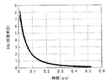
上述したように、Ids補正期間P22では、駆動トランジスタDRTrのドレインからソースに電流Idsが流れ、ソース電圧Vsが上昇し、ゲート・ソース間電圧Vgsが徐々に低下する。これにより、駆動トランジスタDRTrのドレインからソースに流れる電流Idsも徐々に低下する。
(About Ids correction)
As described above, in the Ids correction period P22, the current Ids flows from the drain to the source of the drive transistor DRTr, the source voltage Vs increases, and the gate-source voltage Vgs gradually decreases. As a result, the current Ids flowing from the drain to the source of the drive transistor DRTr also gradually decreases.
図44は、ある画素電圧Vsigを与えたときの電流Idsの時間変化を表すものである。この図44は、互いに異なる複数のプロセス条件でトランジスタを製造した場合を想定したシミュレーション結果を示している。図44に示したように、電流Idsは、時間が経過するとともに徐々に低下する。その際、電流Idsの時間変化は、プロセス条件に依存して互いに異なったものとなる。具体的には、例えば、電流値Idsが大きい場合(移動度μが高く閾値Vthが低い場合)にはより早く低下し、電流値Idsが小さい場合(移動度μが低く閾値Vthが高い場合)にはより遅く低下する。 FIG. 44 shows the time change of the current Ids when a certain pixel voltage Vsig is given. FIG. 44 shows a simulation result assuming that a transistor is manufactured under a plurality of different process conditions. As shown in FIG. 44, the current Ids gradually decreases with time. At that time, the time change of the current Ids differs depending on the process conditions. Specifically, for example, when the current value Ids is large (when the mobility μ is high and the threshold value Vth is low), it decreases faster, and when the current value Ids is small (when the mobility μ is low and the threshold value Vth is high). Will fall later.
図45は、図44に示した電流Idsのばらつきの時間依存性を表すものである。特性W1は、標準偏差を平均値で割ったもの(σ/ave.)を示し、特性W2は、ばらつき幅を平均値で割ったもの(Range/ave.)を示す。このように、電流Idsのばらつきは、ある時間t(例えば特性W2では時間tw)において極小値をとる。つまり、Ids補正を時間twの長さで行うと、電流Idsのばらつき幅を最も小さくすることができる。 FIG. 45 shows the time dependency of the variation of the current Ids shown in FIG. The characteristic W1 represents the standard deviation divided by the average value (σ / ave.), And the characteristic W2 represents the variation width divided by the average value (Range / ave.). Thus, the variation of the current Ids takes a minimum value at a certain time t (for example, the time tw in the characteristic W2). That is, if the Ids correction is performed for the length of time tw, the variation width of the current Ids can be minimized.
表示装置2では、このように、Ids補正期間P22の長さ(図43におけるタイミングt22〜t23)を、電流Idsのばらつきが小さくなる長さ(例えば時間tw)に設定している。これにより、タイミングt23における電流Idsのばらつきを抑えることができるため、画質の低下を抑えることができる。
In the
(画質について)
表示装置2では、図41に示したように、アノード312W,312Gを、3本のデータ線DTLと重なるように配置し、アノード312Rを、データ線DTLと重ならないように配置している。これにより、以下に示すように、画質を高めることができる。
(About image quality)
In the
すなわち、アノード312W,312Gを3本のデータ線DTLと重なるように配置することにより、アノード312W,312Gの面積を広くすることができ、開口部WINを広くすることができる。このように開口部WINを広くした場合には、開口部WINが狭い場合に比べて、同じ発光輝度を実現するための、発光層230における電流密度を低くすることができる。よって、表示装置2では、発光層230の経時劣化(いわゆる焼き付き)を抑えることができ、画質を高めることができる。
That is, by arranging the anodes 312W and 312G so as to overlap the three data lines DTL, the areas of the anodes 312W and 312G can be increased, and the opening WIN can be increased. Thus, when the opening WIN is widened, the current density in the
その際、アノード312W,312Gが3本のデータ線DTLと重なっているため、これらの3本のデータ線DTLにおける信号Sigが、カップリングにより、アノード312W,312Gにノイズとして伝わってしまうおそれがある。しかしながら、アノード312W,312Gに生ずるノイズは、3つの信号Sigからのノイズの和になるため、互いに打ち消し合うことにより、画質への影響を低減することができる。すなわち、図42に示したように、信号Sigは、上記第1の実施の形態の場合と異なり電圧Vofsを含まず、複数の画素電圧Vsigが連なるものであるため、1水平期間(1H)ごとの遷移タイミングttでは、電圧が上昇する方向の遷移(立ち上がり遷移)と、電圧が下降する方向の遷移(立ち下がり遷移)のいずれも生じうる。よって、ある遷移タイミングttにおける3つの信号Sigに、立ち上がり遷移と立ち下がり遷移の両方が生ずる場合には、アノード312W,312Gに生ずるノイズが互いに打ち消し合うため、ノイズを抑えることができ、画質を高めることができる。 At this time, since the anodes 312W and 312G overlap with the three data lines DTL, the signals Sig on these three data lines DTL may be transmitted to the anodes 312W and 312G as noise due to the coupling. . However, since the noise generated in the anodes 312W and 312G is the sum of the noises from the three signals Sig, the influence on the image quality can be reduced by canceling each other. That is, as shown in FIG. 42, unlike the case of the first embodiment, the signal Sig does not include the voltage Vofs, and a plurality of pixel voltages Vsig are connected. Therefore, every one horizontal period (1H). At the transition timing tt, both a transition in the direction in which the voltage increases (rising transition) and a transition in the direction in which the voltage decreases (falling transition) can occur. Therefore, when both the rising transition and the falling transition occur in the three signals Sig at a certain transition timing tt, the noise generated in the anodes 312W and 312G cancels each other, so that the noise can be suppressed and the image quality is improved. be able to.
以上のように本実施の形態では、アノードを複数の信号線と重ねて配置するとともに、複数の画素電圧を連ねて信号Sigを構成したので、画質を高めることができる。その他の効果は、上記第1の実施の形態の場合と同様である。 As described above, in this embodiment, since the anode is arranged so as to overlap with a plurality of signal lines and the signal Sig is configured by connecting a plurality of pixel voltages, the image quality can be improved. Other effects are the same as in the case of the first embodiment.
[変形例2−1]
上記実施の形態では、走査信号WSの立ち下がり部分の電圧が短時間で変化するものとしたが、これに限定されるものではなく、これに代えて、例えば、この立ち下がり部分の電圧が徐々に下がるようにしてもよい。以下に、本変形例について、詳細に説明する。
[Modification 2-1]
In the above embodiment, the voltage at the falling portion of the scanning signal WS changes in a short time. However, the present invention is not limited to this. For example, the voltage at the falling portion gradually increases. You may make it go down. Below, this modification is demonstrated in detail.
図46は、本変形例に係る表示装置2Aにおける表示動作のタイミング図を表すものであり、(A)は走査信号WSの波形を示し、(B)は電源信号DSの波形を示し、(C)は信号Sigの波形を示し、(D)は駆動トランジスタDRTrのゲート電圧Vgの波形を示し、(E)は駆動トランジスタDRTrのソース電圧Vsの波形を示す。 46A and 46B are timing charts of the display operation in the display device 2A according to the present modification, where FIG. 46A shows the waveform of the scanning signal WS, FIG. 46B shows the waveform of the power supply signal DS, and (C ) Shows the waveform of the signal Sig, (D) shows the waveform of the gate voltage Vg of the drive transistor DRTr, and (E) shows the waveform of the source voltage Vs of the drive transistor DRTr.
まず、本変形例に係る駆動部50Aは、タイミングt21〜t22の期間(書込期間P21)において、上記第2の実施の形態の場合と同様に、サブ画素11に対して画素電圧Vsigの書込みを行うとともに、サブ画素11を初期化する。 First, the driving unit 50A according to the present modification writes the pixel voltage Vsig to the sub-pixel 11 during the period from the timing t21 to t22 (writing period P21), as in the case of the second embodiment. And the sub-pixel 11 is initialized.
次に、駆動部50Aは、タイミングt22〜t29の期間(Ids補正期間P22)において、上記第2の実施の形態に係る表示部40と同様に、サブ画素11に対してIds補正を行う。その際、本変形例に係る走査線駆動部23Aは、波形の立ち下がり部分の電圧が徐々に下がる走査信号WSを生成する(図46(A))。これにより、画素電圧Vsigのレベルにより、Ids補正期間P22の時間の長さ(タイミングt22〜t29)が異なるように動作する。
Next, in the period from timing t22 to t29 (Ids correction period P22 ), the drive unit 50A performs Ids correction on the sub-pixel 11 in the same manner as the
図47は、Ids補正動作のタイミング図を表すものであり、(A)は走査信号WSの波形を示し、(B)は電源信号DSの波形を示す。書込トランジスタWSTrは、走査信号WSの電圧が、(画素電圧Vsig+閾値電圧Vth)よりも高い場合にはオン状態になり、(画素電圧Vsig+閾値電圧Vth)よりも低い場合にはオフ状態になる。走査信号WSは、立ち下がりの際、図47(A)に示したように、電圧が徐々に低下する。よって、この書込トランジスタWSTrがオン状態からオフ状態に変化するタイミングt29は、画素電圧Vsigのレベルに依存する。すなわち、Ids補正期間P22の時間の長さは、画素電圧Vsigのレベルに依存する。具体的には、Ids補正期間P22の時間は、画素電圧Vsigのレベルが高いほど短く、画素電圧Vsigのレベルが低いほど長くなる。 47A and 47B are timing charts of the Ids correction operation. FIG. 47A shows the waveform of the scanning signal WS, and FIG. 47B shows the waveform of the power supply signal DS. The write transistor WSTr is turned on when the voltage of the scanning signal WS is higher than (pixel voltage Vsig + threshold voltage Vth), and is turned off when lower than (pixel voltage Vsig + threshold voltage Vth). . When the scanning signal WS falls, as shown in FIG. 47A, the voltage gradually decreases. Therefore, the timing t29 at which the write transistor WSTr changes from the on state to the off state depends on the level of the pixel voltage Vsig. That is, the length of the Ids correction period P22 depends on the level of the pixel voltage Vsig. Specifically, the time of the Ids correction period P22 is shorter as the level of the pixel voltage Vsig is higher, and is longer as the level of the pixel voltage Vsig is lower.
そして、Ids補正が終了した後、駆動部50Aは、タイミングt29以降の期間(発光期間P23)において、上記第2の実施の形態の場合と同様に、サブ画素11を発光させる。 After the completion of the Ids correction, the driving unit 50A causes the sub-pixel 11 to emit light in the period after the timing t29 (light emission period P23), as in the case of the second embodiment.
このように、表示装置2Aでは、走査信号WSの波形の立ち下がり部分の電圧が徐々に下がるようにしている。これにより、以下に示すように、画質を高めることができる。 Thus, in the display device 2A, the voltage at the falling portion of the waveform of the scanning signal WS is gradually lowered. As a result, the image quality can be improved as described below.
図44,45に示したように、電流Idsのばらつきは、ある時間t(例えば特性W2では時間tw)において極小値をとる。この電流Idsのばらつきが極小値になる時間は、画素電圧Vsigに応じて変化する。 As shown in FIGS. 44 and 45, the variation of the current Ids takes a minimum value at a certain time t (for example, the time tw in the characteristic W2). The time during which the variation of the current Ids is minimal varies depending on the pixel voltage Vsig.
図48は、電流Idsのばらつきが極小値になる時間と、画素電圧Vsigとの関係を表すものである。このように、電流Idsのばらつきが極小値になる時間は、画素電圧Vsigの電圧が高いほど短くなり、画素電圧Vsigの電圧が低いほど長くなる。すなわち、Ids補正期間P22の時間を、画素電圧Vsigの電圧が高いほど短くし、画素電圧Vsigの電圧が低いほど長くすれば、画素電圧Vsigによらず、タイミングt29における電流Idsのばらつきを抑えることができる。 FIG. 48 shows the relationship between the time when the variation of the current Ids becomes the minimum value and the pixel voltage Vsig. As described above, the time during which the variation of the current Ids is minimized is shorter as the pixel voltage Vsig is higher, and is longer as the pixel voltage Vsig is lower. That is, if the time of the Ids correction period P22 is shortened as the voltage of the pixel voltage Vsig is increased and is increased as the voltage of the pixel voltage Vsig is decreased, the variation in the current Ids at the timing t29 is suppressed regardless of the pixel voltage Vsig. Can do.
表示装置2Aでは、このように画素電圧VsigによってIds補正期間P22の時間の長さを変化させるために、走査信号WSの立ち下がり部分の電圧を徐々に下げるようにしている。具体的には、図48に示した特性を実現できるように、走査信号WSの立ち下がり部分の波形を生成している。これにより、画素電圧Vsigの電圧によらず、電流Idsのばらつきを抑えることができ、画質の低下を抑えることができる。 In the display device 2A, in order to change the length of the Ids correction period P22 by the pixel voltage Vsig as described above, the voltage at the falling portion of the scanning signal WS is gradually decreased. Specifically, the waveform of the falling portion of the scanning signal WS is generated so as to realize the characteristics shown in FIG. As a result, variations in the current Ids can be suppressed regardless of the pixel voltage Vsig, and deterioration in image quality can be suppressed.
なお、このような走査信号WSの波形を生成する方法については、例えば、特開2008−9198に記載がある。 A method for generating such a waveform of the scanning signal WS is described in, for example, Japanese Patent Application Laid-Open No. 2008-9198.
[変形例2−2]
上記実施の形態では、Ids補正を行うようにしたが、これに限定されるものではなく、これに代えて、このIds補正を行わないようにしてもよい。以下に、本変形例について詳細に説明する。
[Modification 2-2]
In the above embodiment, the Ids correction is performed. However, the present invention is not limited to this. Instead, the Ids correction may not be performed. Below, this modification is demonstrated in detail.
図49は、本変形例に係る表示装置2Bにおける表示動作のタイミング図を表すものであり、(A)は走査信号WSの波形を示し、(B)は信号Sigの波形を示し、(C)は駆動トランジスタDRTrのゲート電圧Vgの波形を示し、(D)は駆動トランジスタDRTrのソース電圧Vsの波形を示す。 FIG. 49 shows a timing chart of the display operation in the display device 2B according to this modification. (A) shows the waveform of the scanning signal WS, (B) shows the waveform of the signal Sig, and (C). Shows the waveform of the gate voltage Vg of the drive transistor DRTr, and (D) shows the waveform of the source voltage Vs of the drive transistor DRTr.
本変形例に係る駆動部50Bは、タイミングt31〜t32の期間(書込期間P31)において、サブ画素11に対する画素電圧Vsigの書込みを行う。具体的には、まず、データ線駆動部57が、タイミングt31において、信号Sigを画素電圧Vsigに設定し(図49(B))、走査線駆動部23が、走査信号WSの電圧を低レベルから高レベルに変化させる(図49(A))。これにより、書込トランジスタWSTrがオン状態になり、駆動トランジスタDRTrのゲート電圧Vgが電圧Vsigに設定される(図49(C))。そして、駆動トランジスタDRTrの電流Idsが発光素子19に流れて、ソース電圧Vsが定まる(図49(D))。このようにして、発光素子19は、タイミングt31以降の期間(発光期間P32)において発光する。
The drive unit 50B according to the present modification writes the pixel voltage Vsig to the sub-pixel 11 during the period from the timing t31 to t32 (writing period P31). Specifically, first, the data
この場合でも、複数の画素電圧を連ねて信号Sigを構成することができるため、上記第2の実施の形態の場合と同様に、画質を高めることができる。 Even in this case, since the signal Sig can be formed by connecting a plurality of pixel voltages, the image quality can be improved as in the case of the second embodiment.
[変形例2−3]
上記実施の形態では、アノード312W,312Gを3本のデータ線DTLと重なるように配置したが、これに限定されるものではなく、これに代えて、例えば、上記第1の実施の形態の場合(図7)と同様に、各アノード212をデータ線DTLと重ならないように配置してもよいし、上記第1の実施の形態の変形例1−5の場合(図23)と同様に、各アノード212を1本のデータ線DTLと重なるように配置してもよい。
[Modification 2-3]
In the above embodiment, the anodes 312W and 312G are arranged so as to overlap with the three data lines DTL. However, the present invention is not limited to this, and instead, for example, in the case of the above first embodiment Similarly to (FIG. 7), each
[変形例2−4]
以上、第2の実施の形態およびその変形例について説明したが、これらのうちの2以上を組み合わせてもよい。また、これらに、上記第1の実施の形態の変形例のうちの1以上を組み合わせてもよい。
[Modification 2-4]
Although the second embodiment and the modifications thereof have been described above, two or more of these may be combined. Moreover, you may combine these with 1 or more of the modifications of the said 1st Embodiment.
<3.適用例>
次に、上記実施の形態および変形例で説明した表示装置の適用例について説明する。
<3. Application example>
Next, application examples of the display device described in the above embodiment and modifications will be described.
図50は、上記実施の形態等の表示装置が適用されるテレビジョン装置の外観を表すものである。このテレビジョン装置は、例えば、フロントパネル511およびフィルターガラス512を含む映像表示画面部510を有している。このテレビジョン装置は、上記実施の形態等に係る表示装置により構成されている。 FIG. 50 illustrates an appearance of a television device to which the display device according to any of the above embodiments is applied. The television apparatus includes a video display screen unit 510 including a front panel 511 and a filter glass 512, for example. This television device is constituted by the display device according to the above-described embodiment and the like.
上記実施の形態等の表示装置は、このようなテレビジョン装置の他、デジタルカメラ、ノート型パーソナルコンピュータ、携帯電話等の携帯端末装置、携帯型ゲーム機、あるいはビデオカメラなどのあらゆる分野の電子機器に適用することが可能である。言い換えると、上記実施の形態等の表示装置は、映像を表示するあらゆる分野の電子機器に適用することが可能である。 The display device according to the above embodiment includes electronic devices in various fields such as a digital camera, a notebook personal computer, a portable terminal device such as a mobile phone, a portable game machine, or a video camera in addition to such a television device. It is possible to apply to. In other words, the display device of the above embodiment and the like can be applied to electronic devices in all fields that display video.
以上、いくつかの実施の形態および変形例、ならびに電子機器への適用例を挙げて本技術を説明したが、本技術はこれらの実施の形態等には限定されず、種々の変形が可能である。 The present technology has been described above with some embodiments and modifications, and application examples to electronic devices. However, the present technology is not limited to these embodiments and the like, and various modifications are possible. is there.
例えば、上記実施の形態等では、書込トランジスタWSTrおよび駆動トランジスタDRTrをNMOSで構成したが、これに限定されるものではなく、これに代えて、これらのトランジスタのうちの一方または双方をPMOSで構成してもよい。 For example, in the above-described embodiment and the like, the write transistor WSTr and the drive transistor DRTr are configured by NMOS. However, the present invention is not limited to this. Instead, one or both of these transistors is configured by PMOS. It may be configured.
また、例えば、上記実施の形態等では、サブ画素をいわゆる「2Tr1C」の構成にしたが、これに限定されるものではなく、その他の素子を追加して構成してもよい。具体的には、例えば、図51に示すサブ画素17のように、発光素子19と並列接続された容量素子Csubを設け、いわゆる「2Tr2C」の構成にしてもよい。また、例えば、図52に示すサブ画素18のように、駆動トランジスタDRTrへの電源信号DSの供給を制御する電源トランジスタDSTrを設け、いわゆる「3Tr1C」の構成にしてもよい。
Further, for example, in the above-described embodiment and the like, the sub-pixel has a so-called “2Tr1C” configuration, but is not limited thereto, and may be configured by adding other elements. Specifically, for example, a capacitor element Csub connected in parallel with the
また、例えば、上記各実施の形態では、表示装置は、有機EL表示素子を有するものとしたが、これに限定されるものではなく、電流駆動型の表示素子を有するものであれば、どのような表示装置であってもよい。 Further, for example, in each of the above embodiments, the display device has an organic EL display element. However, the display device is not limited to this, and any display device having a current drive type display element may be used. A simple display device may be used.
なお、本技術は以下のような構成とすることができる。 In addition, this technique can be set as the following structures.
(1)第1の基本色光を発する第1の画素と、第2の基本色光を発する第2の画素と、基本色光以外の一の色光を発する非基本色画素との組み合わせから構成される第1の画素セットと、
前記第1の基本色光を発する第1の画素と、第3の基本色光を発する第3の画素と、前記一の色光を発する非基本色画素との組み合わせから構成される第2の画素セットと
を備え、
前記第1の画素セットおよび前記第2の画素セットは、第1の方向および前記第1の方向と交差する第2の方向のいずれか一方または双方において、交互に配置されている
表示装置。
(1) A first pixel composed of a combination of a first pixel that emits first basic color light, a second pixel that emits second basic color light, and a non-basic color pixel that emits one color light other than the basic color light. 1 pixel set,
A second pixel set comprising a combination of a first pixel that emits the first basic color light, a third pixel that emits a third basic color light, and a non-basic color pixel that emits the one color light; With
The first pixel set and the second pixel set are alternately arranged in one or both of a first direction and a second direction intersecting the first direction.
(2)前記第1の方向に延伸する複数の信号線をさらに備え、
前記第1の画素、前記第2の画素、前記第3の画素、および前記非基本色画素は、それぞれ、画素電極を含む発光素子を有し、
前記第1の画素の画素電極は、前記複数の信号線のうちの、その第1の画素が属する画素セットの配置領域内に配置された所定数の信号線のいずれとも重なるように配置され、
前記非基本色画素の画素電極は、前記複数の信号線のうちの、その非基本色画素が属する画素セットの配置領域内に配置された所定数の信号線のいずれとも重なるように配置されている
前記(1)に記載の表示装置。
(2) further comprising a plurality of signal lines extending in the first direction;
The first pixel, the second pixel, the third pixel, and the non-basic color pixel each have a light emitting element including a pixel electrode,
The pixel electrode of the first pixel is arranged so as to overlap with any of a predetermined number of signal lines arranged in the arrangement region of the pixel set to which the first pixel belongs among the plurality of signal lines,
The pixel electrode of the non-basic color pixel is arranged so as to overlap with any of a predetermined number of signal lines arranged in the arrangement region of the pixel set to which the non-basic color pixel belongs among the plurality of signal lines. The display device according to (1).
(3)前記第2の画素の画素電極および前記第3の画素の画素電極は、前記複数の信号線のいずれとも重ならないように配置されている
前記(2)に記載の表示装置。
(3) The display device according to (2), wherein the pixel electrode of the second pixel and the pixel electrode of the third pixel are arranged so as not to overlap any of the plurality of signal lines.
(4)前記第1の方向に延伸する複数の信号線をさらに備え、
前記第1の画素、前記第2の画素、前記第3の画素、および前記非基本色画素は、それぞれ、前記複数の信号線のうちの1本と重なるように配置された画素電極を含む発光素子を有する
前記(1)に記載の表示装置。
(4) further comprising a plurality of signal lines extending in the first direction;
Each of the first pixel, the second pixel, the third pixel, and the non-basic color pixel includes a pixel electrode arranged to overlap one of the plurality of signal lines. The display device according to (1), including an element.
(5)前記第1の方向に延伸する複数の信号線をさらに備え、
前記第1の画素、前記第2の画素、前記第3の画素、および前記非基本色画素は、それぞれ、前記複数の信号線のいずれとも重ならないように配置された画素電極を含む発光素子を有する
前記(1)に記載の表示装置。
(5) further comprising a plurality of signal lines extending in the first direction;
Each of the first pixel, the second pixel, the third pixel, and the non-basic color pixel includes a light emitting element including a pixel electrode disposed so as not to overlap any of the plurality of signal lines. The display device according to (1).
(6)前記信号線に画素信号を印加する駆動部をさらに備え、
前記画素信号では、各画素の輝度を画定する輝度信号部分が時間軸上で連なっている
前記(2)から(5)のいずれかに記載の表示装置。
(6) a drive unit for applying a pixel signal to the signal line;
The display device according to any one of (2) to (5), wherein in the pixel signal, a luminance signal portion that defines luminance of each pixel is continuous on a time axis.
(7)前記信号線に画素信号を印加する駆動部をさらに備え、
前記画素信号は、直流信号部分と、各画素の輝度を画定する輝度信号部分とを含み、
前記輝度信号部分と前記直流信号部分とが時間軸上で交互に配置されている
前記(4)または(5)に記載の表示装置。
(7) It further includes a drive unit that applies a pixel signal to the signal line,
The pixel signal includes a direct current signal portion and a luminance signal portion that defines the luminance of each pixel;
The display device according to (4) or (5), wherein the luminance signal portion and the DC signal portion are alternately arranged on a time axis.
(8)前記第2の基本色光に対応する第1の輝度情報マップに対してフィルタ処理を行うとともに、前記第3の基本色光に対応する第2の輝度情報マップに対してフィルタ処理を行うフィルタ部と、
フィルタ処理された第1の輝度情報マップから、前記第1の画素セットに対応する位置の第1の輝度情報を抽出するとともに、フィルタ処理された第2の輝度情報マップから、前記第2の画素セットに対応する位置の第2の輝度情報を抽出する輝度情報抽出部と
をさらに備え、
前記駆動部は、前記第1の輝度情報に基づいて前記第2の画素に対応する前記輝度信号部分を生成するとともに、前記第2の輝度情報に基づいて前記第3の画素に対応する前記輝度信号部分を生成する
前記(6)または(7)に記載の表示装置。
(8) A filter that performs filter processing on the first luminance information map corresponding to the second basic color light and performs filter processing on the second luminance information map corresponding to the third basic color light And
First luminance information at a position corresponding to the first pixel set is extracted from the filtered first luminance information map, and the second pixel is extracted from the filtered second luminance information map. A luminance information extraction unit that extracts second luminance information at a position corresponding to the set;
The drive unit generates the luminance signal portion corresponding to the second pixel based on the first luminance information, and the luminance corresponding to the third pixel based on the second luminance information. The display device according to (6) or (7), wherein a signal portion is generated.
(9)前記第1の方向に延伸する複数の信号線をさらに備え、
前記第1の画素セットが、第1の画素セル内に配置され、
前記第2の画素セットが、第2の画素セル内に配置され、
前記第1の画素セルにおいて、前記第1の画素および前記非基本色画素は、前記第1の方向に配列されるとともに、前記第2の画素と前記第2の方向において配列され、
前記第2の画素セルにおいて、前記第1の画素および前記非基本色画素は、前記第1の方向に配列されるとともに、前記第3の画素と前記第2の方向において配列されている
前記(1)から(8)のいずれかに記載の表示装置。
(9) further comprising a plurality of signal lines extending in the first direction;
The first pixel set is disposed in a first pixel cell;
The second pixel set is disposed in a second pixel cell;
In the first pixel cell, the first pixel and the non-basic color pixel are arranged in the first direction, and are arranged in the second direction with the second pixel.
In the second pixel cell, the first pixel and the non-basic color pixel are arranged in the first direction, and are arranged in the second direction with the third pixel. The display device according to any one of 1) to (8).
(10)前記第1の方向に延伸する複数の信号線をさらに備え、
前記第1の画素セットが、第1の画素セル内に配置され、
前記第2の画素セットが、第2の画素セル内に配置され、
前記第1の画素セルにおいて、前記第1の画素、前記第2の画素、および前記非基本色画素は、前記第2の方向に配列され、
前記第2の画素セルにおいて、前記第1の画素、前記第3の画素、および前記非基本色画素は、前記第2の方向に配列されている
前記(1)から(8)のいずれかに記載の表示装置。
(10) It further comprises a plurality of signal lines extending in the first direction,
The first pixel set is disposed in a first pixel cell;
The second pixel set is disposed in a second pixel cell;
In the first pixel cell, the first pixel, the second pixel, and the non-basic color pixel are arranged in the second direction,
In the second pixel cell, the first pixel, the third pixel, and the non-basic color pixel are arranged in the second direction. Any one of (1) to (8) The display device described.
(11)前記第1の方向に延伸する複数の信号線をさらに備え、
前記第1の画素セットが、第1の画素セル内に配置され、
前記第2の画素セットが、第2の画素セル内に配置され、
前記第1の画素、前記第2の画素、前記第3の画素、および前記非基本色画素の開口部は円形または楕円形であり、
前記第1の画素セルにおいて、前記第1の画素、前記第2の画素、および前記非基本色画素は、互いに隣り合うように配置されるとともに、そのうちの2つは、前記第2の方向に配列され、
前記第2の画素セルにおいて、前記第1の画素、前記第3の画素、および前記非基本色画素は、互いに隣り合うように配置されるとともに、そのうちの2つは、前記第2の方向に配列されている
前記(1)から(8)のいずれかに記載の表示装置。
(11) further comprising a plurality of signal lines extending in the first direction;
The first pixel set is disposed in a first pixel cell;
The second pixel set is disposed in a second pixel cell;
The openings of the first pixel, the second pixel, the third pixel, and the non-basic color pixel are circular or elliptical,
In the first pixel cell, the first pixel, the second pixel, and the non-basic color pixel are arranged adjacent to each other, and two of them are arranged in the second direction. Arranged,
In the second pixel cell, the first pixel, the third pixel, and the non-basic color pixel are arranged adjacent to each other, and two of them are arranged in the second direction. The display device according to any one of (1) to (8), wherein the display device is arranged.
(12)前記第1の画素セットは、複数の第1の画素セル内に、互いに異なる配置パターンとなるように配置され、
前記第2の画素セットは、複数の第2の画素セル内に、互いに異なる配置パターンとなるように配置されている
前記(9)から(11)のいずれかに記載の表示装置。
(12) The first pixel sets are arranged in a plurality of first pixel cells so as to have different arrangement patterns,
The display device according to any one of (9) to (11), wherein the second pixel set is arranged in a plurality of second pixel cells so as to have different arrangement patterns.
(13)前記第2の画素における開口領域、および前記第3の画素における開口領域は、前記第1の画素における開口領域、および前記非基本色画素における開口領域のいずれよりも大きい
前記(1)から(12)のいずれかに記載の表示装置。
(13) The opening area in the second pixel and the opening area in the third pixel are larger than any of the opening area in the first pixel and the opening area in the non-basic color pixel. To (12).
(14)前記第1の画素における開口領域は、前記非基本色画素の開口領域以上の大きさである
前記(13)に記載の表示装置。
(14) The display device according to (13), wherein an opening area in the first pixel is larger than an opening area of the non-basic color pixel.
(15)前記第1の基本色光は緑色光であり、
前記第2の基本色光は青色光であり、
前記第3の基本色光は赤色光である
前記(1)から(14)のいずれかに記載の表示装置。
(15) The first basic color light is green light,
The second basic color light is blue light;
The display device according to any one of (1) to (14), wherein the third basic color light is red light.
(16)前記第1の画素、前記第2の画素、前記第3の画素、および前記非基本色画素は、それぞれ、
容量素子と、
ドレインと、前記容量素子の一端に接続されたゲートと、前記容量素子の他端に接続されたソースとを含むトランジスタと
を有する
前記(1)から(15)のいずれかに記載の表示装置。
(16) The first pixel, the second pixel, the third pixel, and the non-basic color pixel are respectively
A capacitive element;
The display device according to any one of (1) to (15), further including: a transistor including a drain, a gate connected to one end of the capacitor, and a source connected to the other end of the capacitor.
(17)表示装置と
前記表示装置に対して動作制御を行う制御部と
を備え、
前記表示装置は、
第1の基本色光を発する第1の画素と、第2の基本色光を発する第2の画素と、基本色光以外の一の色光を発する非基本色画素との組み合わせから構成される第1の画素セットと、
前記第1の基本色光を発する第1の画素と、第3の基本色光を発する第3の画素と、前記一の色光を発する非基本色画素との組み合わせから構成される第2の画素セットと
を備え、
前記第1の画素セットおよび前記第2の画素セットは、第1の方向および前記第1の方向と交差する第2の方向のいずれか一方または双方において、交互に配置されている
電子機器。
(17) a display device and a control unit that performs operation control on the display device;
The display device
A first pixel composed of a combination of a first pixel that emits first basic color light, a second pixel that emits second basic color light, and a non-basic color pixel that emits one color light other than the basic color light Set,
A second pixel set comprising a combination of a first pixel that emits the first basic color light, a third pixel that emits a third basic color light, and a non-basic color pixel that emits the one color light; With
The electronic device in which the first pixel set and the second pixel set are alternately arranged in one or both of a first direction and a second direction intersecting with the first direction.
1,2…表示装置、10,10B〜10M,40…表示部、11,11R,11G,11B,11W,14R,14G,14B,14W,17,18…サブ画素、15,15R,15G,15B,15W,16,16R,16G,16B,16W…回路領域、19…発光素子、20,50…駆動部、22…タイミング生成部、23…走査線駆動部、26…電源線駆動部、27,27N,57…データ線駆動部、30…映像信号処理部、31…リニアガンマ変換部、32…RGBW変換部、33R,33B…フィルタ処理部、34R,34B…輝度情報抽出部、35…信号処理部、36…パネルガンマ変換部、201…ゲート、202…絶縁層、203…ポリシリコン、204…絶縁層、205…コンタクト/配線、211…絶縁層、212,212R,212G,212B,212W,232,312,312R,312G,312B,312W…アノード、213,213L,221…絶縁層、214…黄色発光層、215…青色発光層、216,236…カソード、217,217L…絶縁層、218,218I,238…カラーフィルタ、219…ブラックマトリクス、220…透明基板、230,230H,230I,230J…発光層、CA,CA1,CA2,CB,CB1,CB2…セル、Cs,Csub…容量素子、DRTr…駆動トランジスタ、DS…電源信号、DSTr…電源トランジスタ、DTL…データ線、H…高さ、MAPR,MAPB…マップ、PL…電源線、P1…初期化期間、P2…Vth補正期間、P3,P13,P15…書込・μ補正期間、P4,P14,P16…発光期間、P21…書込期間、P22…Ids補正期間、P23…発光期間、P31…書込期間、P32…発光期間、R1,R2…直径、Sdisp,Sdisp2…映像信号、Sig…信号、Ssync…同期信号、S31,S34,S35…映像信号、SR32,SG32,SB32,SW32,SR33,SB33,SR34,SB34…信号、Vcath,Vccp,Vini,Vofs…電圧、Vsig…画素電圧、WIN…開口部、WS,WSA,WSB…走査信号、WSL,WSAL,WSBL…走査線、WSTr…書込トランジスタ。 1, 2, ... Display device, 10, 10B to 10M, 40 ... Display unit, 11, 11R, 11G, 11B, 11W, 14R, 14G, 14B, 14W, 17, 18 ... Subpixel, 15, 15R, 15G, 15B , 15W, 16, 16R, 16G, 16B, 16W ... circuit region, 19 ... light emitting element, 20, 50 ... drive unit, 22 ... timing generation unit, 23 ... scanning line drive unit, 26 ... power line drive unit, 27, 27N, 57: Data line drive unit, 30: Video signal processing unit, 31 ... Linear gamma conversion unit, 32 ... RGBW conversion unit, 33R, 33B ... Filter processing unit, 34R, 34B ... Luminance information extraction unit, 35 ... Signal processing 36: Panel gamma conversion unit, 201: Gate, 202 ... Insulating layer, 203 ... Polysilicon, 204 ... Insulating layer, 205 ... Contact / wiring, 211 ... Insulating layer, 212, 12R, 212G, 212B, 212W, 232, 312, 312R, 312G, 312B, 312W ... anode, 213, 213L, 221 ... insulating layer, 214 ... yellow light emitting layer, 215 ... blue light emitting layer, 216, 236 ... cathode, 217 , 217L ... insulating layer, 218, 218I, 238 ... color filter, 219 ... black matrix, 220 ... transparent substrate, 230, 230H, 230I, 230J ... light emitting layer, CA, CA1, CA2, CB, CB1, CB2 ... cell, Cs, Csub: Capacitance element, DRTr ... Drive transistor, DS ... Power supply signal, DSTr ... Power supply transistor, DTL ... Data line, H ... Height, MAPR, MAPB ... Map, PL ... Power supply line, P1 ... Initialization period, P2 ... Vth correction period, P3, P13, P15 ... Write / μ correction period, P4, P1 , P16 ... light emission period, P21 ... writing period, P22 ... Ids correction period, P23 ... light emission period, P31 ... writing period, P32 ... light emission period, R1, R2 ... diameter, Sdisp, Sdisp2 ... video signal, Sig ... signal , Ssync ... synchronization signal, S31, S34, S35 ... video signal, SR32, SG32, SB32, SW32, SR33, SB33, SR34, SB34 ... signal, Vcath, Vccp, Vini, Vofs ... voltage, Vsig ... pixel voltage, WIN ... Opening, WS, WSA, WSB... Scanning signal, WSL, WSAL, WSBL... Scanning line, WSTr.
Claims (13)
前記第1の基本色光を発する第1の画素と、第3の基本色光を発する第3の画素と、前記一の色光を発する非基本色画素との組み合わせから構成される第2の画素セットと、
第1の方向に延伸する複数の信号線と
を備え、
前記第1の画素セットおよび前記第2の画素セットは、前記第1の方向および前記第1の方向と交差する第2の方向のいずれか一方または双方において、交互に配置され、
前記第1の画素、前記第2の画素、前記第3の画素、および前記非基本色画素は、それぞれ、画素電極を含む発光素子を有し、
前記第1の画素の画素電極は、前記複数の信号線のうちの、その第1の画素が属する画素セットの配置領域内に配置された所定数の信号線のいずれとも重なるように配置され、
前記非基本色画素の画素電極は、前記複数の信号線のうちの、その非基本色画素が属する画素セットの配置領域内に配置された所定数の信号線のいずれとも重なるように配置されている
表示装置。 A first pixel composed of a combination of a first pixel that emits first basic color light, a second pixel that emits second basic color light, and a non-basic color pixel that emits one color light other than the basic color light Set,
A second pixel set comprising a combination of a first pixel that emits the first basic color light, a third pixel that emits a third basic color light, and a non-basic color pixel that emits the one color light; ,
A plurality of signal lines extending in the first direction,
The first pixel set and the second pixel set are alternately arranged in one or both of the first direction and the second direction intersecting the first direction,
The first pixel, the second pixel, the third pixel, and the non-basic color pixel each have a light emitting element including a pixel electrode,
The pixel electrode of the first pixel is arranged so as to overlap with any of a predetermined number of signal lines arranged in the arrangement region of the pixel set to which the first pixel belongs among the plurality of signal lines,
The pixel electrode of the non-basic color pixel is arranged so as to overlap with any of a predetermined number of signal lines arranged in the arrangement region of the pixel set to which the non-basic color pixel belongs among the plurality of signal lines. Display device.
請求項1に記載の表示装置。 The display device according to claim 1, wherein the pixel electrode of the second pixel and the pixel electrode of the third pixel are arranged so as not to overlap any of the plurality of signal lines.
前記画素信号では、各画素の輝度を画定する輝度信号部分が時間軸上で連なっている
請求項1または請求項2に記載の表示装置。 A drive unit for applying a pixel signal to the signal line;
The display device according to claim 1, wherein in the pixel signal, a luminance signal portion that defines luminance of each pixel is continuous on a time axis.
フィルタ処理された第1の輝度情報マップから、前記第1の画素セットに対応する位置の第1の輝度情報を抽出するとともに、フィルタ処理された第2の輝度情報マップから、前記第2の画素セットに対応する位置の第2の輝度情報を抽出する輝度情報抽出部と
をさらに備え、
前記駆動部は、前記第1の輝度情報に基づいて前記第2の画素に対応する前記輝度信号部分を生成するとともに、前記第2の輝度情報に基づいて前記第3の画素に対応する前記輝度信号部分を生成する
請求項3に記載の表示装置。 A filter unit that performs a filtering process on the first luminance information map corresponding to the second basic color light and performs a filtering process on the second luminance information map corresponding to the third basic color light;
First luminance information at a position corresponding to the first pixel set is extracted from the filtered first luminance information map, and the second pixel is extracted from the filtered second luminance information map. A luminance information extraction unit that extracts second luminance information at a position corresponding to the set;
The drive unit generates the luminance signal portion corresponding to the second pixel based on the first luminance information, and the luminance corresponding to the third pixel based on the second luminance information. The display device according to claim 3, wherein the signal portion is generated.
前記第2の画素セットが、第2の画素セル内に配置され、
前記第1の画素セルにおいて、前記第1の画素および前記非基本色画素は、前記第1の方向に配列されるとともに、前記第2の画素と前記第2の方向において配列され、
前記第2の画素セルにおいて、前記第1の画素および前記非基本色画素は、前記第1の方向に配列されるとともに、前記第3の画素と前記第2の方向において配列されている
請求項1から請求項4のいずれか一項に記載の表示装置。 Before SL first pixel set is disposed on the first pixel in the cell,
The second pixel set is disposed in a second pixel cell;
In the first pixel cell, the first pixel and the non-basic color pixel are arranged in the first direction, and are arranged in the second direction with the second pixel.
The first pixel and the non-basic color pixel in the second pixel cell are arranged in the first direction and in the second direction with the third pixel. The display device according to any one of claims 1 to 4.
前記第2の画素セットが、第2の画素セル内に配置され、
前記第1の画素セルにおいて、前記第1の画素、前記第2の画素、および前記非基本色画素は、前記第2の方向に配列され、
前記第2の画素セルにおいて、前記第1の画素、前記第3の画素、および前記非基本色画素は、前記第2の方向に配列されている
請求項1から請求項4のいずれか一項に記載の表示装置。 Before SL first pixel set is disposed on the first pixel in the cell,
The second pixel set is disposed in a second pixel cell;
In the first pixel cell, the first pixel, the second pixel, and the non-basic color pixel are arranged in the second direction,
5. The first pixel, the third pixel, and the non-basic color pixel are arranged in the second direction in the second pixel cell. The display device described in 1.
前記第2の画素セットが、第2の画素セル内に配置され、
前記第1の画素、前記第2の画素、前記第3の画素、および前記非基本色画素の開口部は円形または楕円形であり、
前記第1の画素セルにおいて、前記第1の画素、前記第2の画素、および前記非基本色画素は、互いに隣り合うように配置されるとともに、そのうちの2つは、前記第2の方向に配列され、
前記第2の画素セルにおいて、前記第1の画素、前記第3の画素、および前記非基本色画素は、互いに隣り合うように配置されるとともに、そのうちの2つは、前記第2の方向に配列されている
請求項1から請求項4のいずれか一項に記載の表示装置。 Before SL first pixel set is disposed on the first pixel in the cell,
The second pixel set is disposed in a second pixel cell;
The openings of the first pixel, the second pixel, the third pixel, and the non-basic color pixel are circular or elliptical,
In the first pixel cell, the first pixel, the second pixel, and the non-basic color pixel are arranged adjacent to each other, and two of them are arranged in the second direction. Arranged,
In the second pixel cell, the first pixel, the third pixel, and the non-basic color pixel are arranged adjacent to each other, and two of them are arranged in the second direction. The display device according to any one of claims 1 to 4, wherein the display devices are arranged.
前記第2の画素セットは、複数の第2の画素セル内に、互いに異なる配置パターンとなるように配置されている
請求項5から請求項7のいずれか一項に記載の表示装置。 The first pixel sets are arranged in a plurality of first pixel cells so as to have different arrangement patterns,
The display device according to any one of claims 5 to 7, wherein the second pixel set is arranged in a plurality of second pixel cells so as to have different arrangement patterns.
請求項1から請求項8のいずれか一項に記載の表示装置。 The opening area in the second pixel and the opening area in the third pixel are larger than any of the opening area in the first pixel and the opening area in the non-basic color pixel. The display device according to any one of the above.
請求項9に記載の表示装置。 The display device according to claim 9, wherein the opening area in the first pixel is larger than the opening area of the non-basic color pixel.
前記第2の基本色光は青色光であり、
前記第3の基本色光は赤色光である
請求項1から請求項10のいずれか一項に記載の表示装置。 The first basic color light is green light;
The second basic color light is blue light;
The display device according to any one of claims 1 to 10, wherein the third basic color light is red light.
容量素子と、
ドレインと、前記容量素子の一端に接続されたゲートと、前記容量素子の他端に接続されたソースとを含むトランジスタと
を有する
請求項1から請求項11のいずれか一項に記載の表示装置。 The first pixel, the second pixel, the third pixel, and the non-basic color pixel are respectively
A capacitive element;
The display device according to claim 1, further comprising: a transistor including a drain, a gate connected to one end of the capacitor, and a source connected to the other end of the capacitor. .
前記表示装置に対して動作制御を行う制御部と
を備え、
前記表示装置は、
第1の基本色光を発する第1の画素と、第2の基本色光を発する第2の画素と、基本色光以外の一の色光を発する非基本色画素との組み合わせから構成される第1の画素セットと、
前記第1の基本色光を発する第1の画素と、第3の基本色光を発する第3の画素と、前記一の色光を発する非基本色画素との組み合わせから構成される第2の画素セットと、
第1の方向に延伸する複数の信号線と
を備え、
前記第1の画素セットおよび前記第2の画素セットは、前記第1の方向および前記第1の方向と交差する第2の方向のいずれか一方または双方において、交互に配置され、
前記第1の画素、前記第2の画素、前記第3の画素、および前記非基本色画素は、それぞれ、画素電極を含む発光素子を有し、
前記第1の画素の画素電極は、前記複数の信号線のうちの、その第1の画素が属する画素セットの配置領域内に配置された所定数の信号線のいずれとも重なるように配置され、
前記非基本色画素の画素電極は、前記複数の信号線のうちの、その非基本色画素が属する画素セットの配置領域内に配置された所定数の信号線のいずれとも重なるように配置されている
電子機器。
A display device and a control unit for controlling the operation of the display device,
The display device
A first pixel composed of a combination of a first pixel that emits first basic color light, a second pixel that emits second basic color light, and a non-basic color pixel that emits one color light other than the basic color light Set,
A second pixel set comprising a combination of a first pixel that emits the first basic color light, a third pixel that emits a third basic color light, and a non-basic color pixel that emits the one color light; ,
A plurality of signal lines extending in the first direction,
The first pixel set and the second pixel set are alternately arranged in one or both of the first direction and the second direction intersecting the first direction,
The first pixel, the second pixel, the third pixel, and the non-basic color pixel each have a light emitting element including a pixel electrode,
The pixel electrode of the first pixel is arranged so as to overlap with any of a predetermined number of signal lines arranged in the arrangement region of the pixel set to which the first pixel belongs among the plurality of signal lines,
The pixel electrode of the non-basic color pixel is arranged so as to overlap with any of a predetermined number of signal lines arranged in the arrangement region of the pixel set to which the non-basic color pixel belongs among the plurality of signal lines. Electronic equipment.
Priority Applications (8)
| Application Number | Priority Date | Filing Date | Title |
|---|---|---|---|
| JP2013062650A JP5849981B2 (en) | 2013-03-25 | 2013-03-25 | Display device and electronic device |
| US14/192,934 US8952374B2 (en) | 2013-03-25 | 2014-02-28 | Display and electronic apparatus |
| TW103107309A TWI637503B (en) | 2013-03-25 | 2014-03-04 | Display and electronic apparatus |
| KR1020140030188A KR102162122B1 (en) | 2013-03-25 | 2014-03-14 | Display and electronic apparatus |
| CN201410101834.1A CN104078001B (en) | 2013-03-25 | 2014-03-18 | Display device and electronic equipment |
| CN201420123876.0U CN203870947U (en) | 2013-03-25 | 2014-03-18 | Display apparatus and electronic device |
| KR1020200121320A KR102339431B1 (en) | 2013-03-25 | 2020-09-21 | Display and electronic apparatus |
| KR1020210175896A KR20210154127A (en) | 2013-03-25 | 2021-12-09 | Display and electronic apparatus |
Applications Claiming Priority (1)
| Application Number | Priority Date | Filing Date | Title |
|---|---|---|---|
| JP2013062650A JP5849981B2 (en) | 2013-03-25 | 2013-03-25 | Display device and electronic device |
Publications (3)
| Publication Number | Publication Date |
|---|---|
| JP2014186258A JP2014186258A (en) | 2014-10-02 |
| JP2014186258A5 JP2014186258A5 (en) | 2015-04-02 |
| JP5849981B2 true JP5849981B2 (en) | 2016-02-03 |
Family
ID=51568466
Family Applications (1)
| Application Number | Title | Priority Date | Filing Date |
|---|---|---|---|
| JP2013062650A Expired - Fee Related JP5849981B2 (en) | 2013-03-25 | 2013-03-25 | Display device and electronic device |
Country Status (5)
| Country | Link |
|---|---|
| US (1) | US8952374B2 (en) |
| JP (1) | JP5849981B2 (en) |
| KR (3) | KR102162122B1 (en) |
| CN (2) | CN104078001B (en) |
| TW (1) | TWI637503B (en) |
Families Citing this family (51)
| Publication number | Priority date | Publication date | Assignee | Title |
|---|---|---|---|---|
| JP2014186257A (en) * | 2013-03-25 | 2014-10-02 | Sony Corp | Display device and electronic apparatus |
| KR102047003B1 (en) * | 2013-04-24 | 2019-11-21 | 삼성디스플레이 주식회사 | Organic Light Emitting Display |
| TWI674671B (en) * | 2013-05-28 | 2019-10-11 | 日商新力股份有限公司 | Display device and electronic device |
| JP6486660B2 (en) * | 2013-11-27 | 2019-03-20 | 株式会社半導体エネルギー研究所 | Display device |
| JP6556998B2 (en) * | 2013-11-28 | 2019-08-07 | 株式会社半導体エネルギー研究所 | Display device |
| TWI745740B (en) * | 2014-05-15 | 2021-11-11 | 日商半導體能源研究所股份有限公司 | Light-emitting element, light-emitting device, electronic device, and lighting device |
| CN104112824A (en) * | 2014-07-09 | 2014-10-22 | 京东方科技集团股份有限公司 | OLED display device, and preparation method and vapor-deposition mask plates thereof |
| JP6453612B2 (en) * | 2014-10-29 | 2019-01-16 | 株式会社ジャパンディスプレイ | Display device |
| CN104407480B (en) * | 2014-11-05 | 2017-05-31 | 深圳市华星光电技术有限公司 | Dot structure and the liquid crystal display panel with the dot structure |
| JP6566289B2 (en) * | 2014-11-26 | 2019-08-28 | Tianma Japan株式会社 | Display device, electro-optical device, electric apparatus, metal mask, and pixel array |
| CN107006096B (en) * | 2014-11-27 | 2019-03-01 | 夏普株式会社 | Light-emitting component, display panel, display device, the manufacturing method of light-emitting component |
| JP6386892B2 (en) * | 2014-11-28 | 2018-09-05 | 株式会社ジャパンディスプレイ | Display device |
| US9933872B2 (en) * | 2014-12-01 | 2018-04-03 | Semiconductor Energy Laboratory Co., Ltd. | Touch panel |
| TWI556048B (en) | 2014-12-02 | 2016-11-01 | 聯詠科技股份有限公司 | Display device and driving module thereof |
| CN105739143B (en) * | 2014-12-10 | 2019-04-09 | 联咏科技股份有限公司 | Display device and its drive module |
| CN105739140B (en) * | 2014-12-10 | 2019-05-24 | 联咏科技股份有限公司 | Display device and its drive module |
| KR102243947B1 (en) * | 2014-12-26 | 2021-04-23 | 엘지디스플레이 주식회사 | Liquid Crystal Display Device |
| JP2016139071A (en) * | 2015-01-29 | 2016-08-04 | 株式会社ジャパンディスプレイ | Display device |
| CN104766875B (en) * | 2015-03-30 | 2019-12-13 | 昆山工研院新型平板显示技术中心有限公司 | pixel arrangement mode sharing blue light emitting layer and organic electroluminescent device |
| CN104716167B (en) * | 2015-04-13 | 2017-07-25 | 京东方科技集团股份有限公司 | A kind of organic elctroluminescent device, its preparation method and display device |
| KR102326806B1 (en) | 2015-04-24 | 2021-11-15 | 엘지디스플레이 주식회사 | Display device having sub pixel array structure |
| KR102306652B1 (en) * | 2015-04-28 | 2021-09-29 | 삼성디스플레이 주식회사 | Display device and driving method thereof |
| JP6499511B2 (en) * | 2015-05-19 | 2019-04-10 | 株式会社ジャパンディスプレイ | Display device |
| CN105304678B (en) * | 2015-09-25 | 2018-11-16 | 上海和辉光电有限公司 | The pixel arrangement structure and mask plate of organic LED display panel |
| US11747531B2 (en) | 2016-02-18 | 2023-09-05 | Chengdu Boe Optoelectronics Technology Co., Ltd. | Display substrate, fine metal mask set and manufacturing method thereof |
| US11448807B2 (en) | 2016-02-18 | 2022-09-20 | Chengdu Boe Optoelectronics Technology Co., Ltd. | Display substrate, fine metal mask set and manufacturing method thereof |
| CN110137213A (en) | 2018-02-09 | 2019-08-16 | 京东方科技集团股份有限公司 | Pixel arrangement structure and its display methods, display base plate |
| CN105679235A (en) * | 2016-03-31 | 2016-06-15 | 广东欧珀移动通信有限公司 | Pixel calling method and device |
| KR101695652B1 (en) * | 2016-04-11 | 2017-01-12 | 엘지디스플레이 주식회사 | Organic light emitting display device and method for fabricating the same |
| CN106229300B (en) * | 2016-08-23 | 2019-03-22 | 武汉华星光电技术有限公司 | Dot structure and production method |
| JP2018072676A (en) * | 2016-11-01 | 2018-05-10 | 株式会社ジャパンディスプレイ | Display device |
| JP6844283B2 (en) * | 2017-02-01 | 2021-03-17 | セイコーエプソン株式会社 | Electro-optics and electronic devices |
| CN109637388B (en) * | 2019-01-31 | 2020-06-16 | 武汉华星光电半导体显示技术有限公司 | Display panel |
| US11574960B2 (en) | 2018-02-09 | 2023-02-07 | Boe Technology Group Co., Ltd. | Pixel arrangement structure, display substrate, display device and mask plate group |
| CN115542617A (en) * | 2018-02-09 | 2022-12-30 | 京东方科技集团股份有限公司 | Display substrate and display device |
| CN108922473B (en) * | 2018-07-26 | 2021-08-20 | 京东方科技集团股份有限公司 | Organic light emitting display panel and driving method thereof |
| CN110838505B (en) * | 2018-08-15 | 2020-11-06 | 云谷(固安)科技有限公司 | Display structure and display device |
| CN109036257B (en) * | 2018-10-24 | 2022-04-29 | 上海天马微电子有限公司 | Display panel, driving method thereof and display device |
| KR20200106589A (en) | 2019-03-04 | 2020-09-15 | 삼성디스플레이 주식회사 | Carrier, apparatus for manufacturing a display apparatus having the same and method for manufacturing a display apparatus |
| RU2721754C1 (en) | 2019-07-31 | 2020-05-21 | Боэ Текнолоджи Груп Ко., Лтд. | Electroluminescent display panel and display device |
| US20220123089A1 (en) | 2019-07-31 | 2022-04-21 | Chengdu Boe Optoelectronics Technology Co., Ltd. | Display substrate and display device |
| JP7420560B2 (en) | 2019-07-31 | 2024-01-23 | 京東方科技集團股▲ふん▼有限公司 | Display substrate and its manufacturing method, display panel, display device |
| KR102604313B1 (en) * | 2019-09-26 | 2023-11-20 | 엘지디스플레이 주식회사 | Light Emitting Display Device |
| JP7321049B2 (en) | 2019-10-11 | 2023-08-04 | キヤノン株式会社 | Light-emitting devices, display devices, photoelectric conversion devices, electronic devices, lighting devices, and moving bodies |
| US11557635B2 (en) * | 2019-12-10 | 2023-01-17 | Samsung Display Co., Ltd. | Display device, mask assembly, and apparatus for manufacturing the display device |
| KR20210077477A (en) * | 2019-12-17 | 2021-06-25 | 엘지디스플레이 주식회사 | Light emitting display apparatus |
| CN111580299A (en) * | 2020-05-19 | 2020-08-25 | 深圳市华星光电半导体显示技术有限公司 | Display panel |
| JP2021190398A (en) | 2020-06-04 | 2021-12-13 | キヤノン株式会社 | Light-emitting device, display device, photoelectric conversion device, electronic apparatus, illumination device, mobile body, and wearable device |
| US20220199739A1 (en) * | 2020-06-29 | 2022-06-23 | Chengdu Boe Optoelectronics Technology Co., Ltd. | Display panel and display device |
| WO2022082331A1 (en) * | 2020-10-19 | 2022-04-28 | Boe Technology Group Co., Ltd. | Array substrate and display apparatus |
| US11749184B1 (en) * | 2023-04-06 | 2023-09-05 | Voxel Inc | LED light emitting pixel arrangement structure and display panel device |
Family Cites Families (19)
| Publication number | Priority date | Publication date | Assignee | Title |
|---|---|---|---|---|
| JP2001313172A (en) * | 2000-02-25 | 2001-11-09 | Seiko Epson Corp | Organic electroluminescent white light source and manufacturing method of the same |
| TW503565B (en) | 2000-06-22 | 2002-09-21 | Semiconductor Energy Lab | Display device |
| JP2002287664A (en) * | 2001-03-23 | 2002-10-04 | Canon Inc | Display panel and its driving method |
| US7583279B2 (en) * | 2004-04-09 | 2009-09-01 | Samsung Electronics Co., Ltd. | Subpixel layouts and arrangements for high brightness displays |
| EP1388818B1 (en) * | 2002-08-10 | 2011-06-22 | Samsung Electronics Co., Ltd. | Method and apparatus for rendering image signal |
| KR100493165B1 (en) | 2002-12-17 | 2005-06-02 | 삼성전자주식회사 | Method and apparatus for rendering image signal |
| JP4443179B2 (en) * | 2003-09-29 | 2010-03-31 | 三洋電機株式会社 | Organic EL panel |
| US7515122B2 (en) * | 2004-06-02 | 2009-04-07 | Eastman Kodak Company | Color display device with enhanced pixel pattern |
| KR101122229B1 (en) * | 2004-10-05 | 2012-03-19 | 삼성전자주식회사 | Four color liquid crystal display |
| US8446435B2 (en) * | 2005-04-22 | 2013-05-21 | Sharp Kabushiki Kaisha | Display device |
| US7602119B2 (en) * | 2005-04-25 | 2009-10-13 | Eastman Kodak Company | OLED with magenta and green emissive layers |
| JP5269305B2 (en) * | 2005-11-17 | 2013-08-21 | 三星ディスプレイ株式會社 | Organic light emitting display |
| JP5403860B2 (en) * | 2006-10-10 | 2014-01-29 | 株式会社ジャパンディスプレイ | Color liquid crystal display device |
| CN101262723B (en) * | 2007-03-05 | 2011-02-02 | 株式会社日立显示器 | Organic electroluminescence display device and method of manufacturing the same |
| JP5428142B2 (en) * | 2007-09-11 | 2014-02-26 | カシオ計算機株式会社 | Manufacturing method of display panel |
| JP4623138B2 (en) * | 2008-05-21 | 2011-02-02 | ソニー株式会社 | Display device and electronic device |
| KR101064466B1 (en) | 2009-07-29 | 2011-09-16 | 삼성모바일디스플레이주식회사 | Organic Light Emitting Display Device |
| KR101679850B1 (en) * | 2009-11-23 | 2016-11-25 | 엘지디스플레이 주식회사 | Organic light emitting diodde desplay device |
| KR20110129531A (en) | 2010-05-26 | 2011-12-02 | 삼성모바일디스플레이주식회사 | Pixel array for organic light emitting display device |
-
2013
- 2013-03-25 JP JP2013062650A patent/JP5849981B2/en not_active Expired - Fee Related
-
2014
- 2014-02-28 US US14/192,934 patent/US8952374B2/en active Active
- 2014-03-04 TW TW103107309A patent/TWI637503B/en not_active IP Right Cessation
- 2014-03-14 KR KR1020140030188A patent/KR102162122B1/en active IP Right Grant
- 2014-03-18 CN CN201410101834.1A patent/CN104078001B/en active Active
- 2014-03-18 CN CN201420123876.0U patent/CN203870947U/en not_active Expired - Lifetime
-
2020
- 2020-09-21 KR KR1020200121320A patent/KR102339431B1/en active IP Right Grant
-
2021
- 2021-12-09 KR KR1020210175896A patent/KR20210154127A/en active IP Right Grant
Also Published As
| Publication number | Publication date |
|---|---|
| US20140284570A1 (en) | 2014-09-25 |
| KR102339431B1 (en) | 2021-12-15 |
| CN104078001B (en) | 2016-11-23 |
| KR20200112773A (en) | 2020-10-05 |
| TW201438224A (en) | 2014-10-01 |
| KR102162122B1 (en) | 2020-10-06 |
| JP2014186258A (en) | 2014-10-02 |
| KR20210154127A (en) | 2021-12-20 |
| CN203870947U (en) | 2014-10-08 |
| KR20140116802A (en) | 2014-10-06 |
| CN104078001A (en) | 2014-10-01 |
| TWI637503B (en) | 2018-10-01 |
| US8952374B2 (en) | 2015-02-10 |
Similar Documents
| Publication | Publication Date | Title |
|---|---|---|
| JP5849981B2 (en) | Display device and electronic device | |
| KR102167309B1 (en) | Display and electronic apparatus | |
| TWI623094B (en) | Display unit and electronic apparatus | |
| US10217404B2 (en) | Display panel, display device and electronic apparatus | |
| US9219087B2 (en) | Display, display drive method, method of manufacturing display, and electronic apparatus | |
| JP4428436B2 (en) | Display device and electronic device | |
| US10504396B2 (en) | Display device and electronic apparatus | |
| JP6159965B2 (en) | Display panel, display device and electronic device | |
| JP2012194256A (en) | Display device and electronic apparatus | |
| JP2014029424A (en) | Display device, electronic apparatus, and display panel drive method | |
| TWI569246B (en) | A display device, a driving device, a driving method, and an electronic device | |
| KR102554380B1 (en) | Light Emitting Display Device | |
| WO2015170614A1 (en) | Display device and electronic apparatus | |
| JP5195409B2 (en) | Display device, pixel layout method of display device, and electronic device | |
| JP2010276734A (en) | Display device, method for driving the display device and electronic equipment |
Legal Events
| Date | Code | Title | Description |
|---|---|---|---|
| A521 | Request for written amendment filed |
Free format text: JAPANESE INTERMEDIATE CODE: A523 Effective date: 20150213 |
|
| A621 | Written request for application examination |
Free format text: JAPANESE INTERMEDIATE CODE: A621 Effective date: 20150213 |
|
| A977 | Report on retrieval |
Free format text: JAPANESE INTERMEDIATE CODE: A971007 Effective date: 20150610 |
|
| A131 | Notification of reasons for refusal |
Free format text: JAPANESE INTERMEDIATE CODE: A131 Effective date: 20150630 |
|
| A521 | Request for written amendment filed |
Free format text: JAPANESE INTERMEDIATE CODE: A523 Effective date: 20150810 |
|
| A131 | Notification of reasons for refusal |
Free format text: JAPANESE INTERMEDIATE CODE: A131 Effective date: 20150902 |
|
| A521 | Request for written amendment filed |
Free format text: JAPANESE INTERMEDIATE CODE: A523 Effective date: 20151009 |
|
| TRDD | Decision of grant or rejection written | ||
| A01 | Written decision to grant a patent or to grant a registration (utility model) |
Free format text: JAPANESE INTERMEDIATE CODE: A01 Effective date: 20151104 |
|
| A61 | First payment of annual fees (during grant procedure) |
Free format text: JAPANESE INTERMEDIATE CODE: A61 Effective date: 20151117 |
|
| R151 | Written notification of patent or utility model registration |
Ref document number: 5849981 Country of ref document: JP Free format text: JAPANESE INTERMEDIATE CODE: R151 |
|
| R250 | Receipt of annual fees |
Free format text: JAPANESE INTERMEDIATE CODE: R250 |
|
| R250 | Receipt of annual fees |
Free format text: JAPANESE INTERMEDIATE CODE: R250 |
|
| R250 | Receipt of annual fees |
Free format text: JAPANESE INTERMEDIATE CODE: R250 |
|
| LAPS | Cancellation because of no payment of annual fees |