JP7451237B2 - RFID inlay - Google Patents
RFID inlay Download PDFInfo
- Publication number
- JP7451237B2 JP7451237B2 JP2020040124A JP2020040124A JP7451237B2 JP 7451237 B2 JP7451237 B2 JP 7451237B2 JP 2020040124 A JP2020040124 A JP 2020040124A JP 2020040124 A JP2020040124 A JP 2020040124A JP 7451237 B2 JP7451237 B2 JP 7451237B2
- Authority
- JP
- Japan
- Prior art keywords
- slit
- antenna pattern
- chip
- base material
- rfid inlay
- Prior art date
- Legal status (The legal status is an assumption and is not a legal conclusion. Google has not performed a legal analysis and makes no representation as to the accuracy of the status listed.)
- Active
Links
Images


Landscapes
- Support Of Aerials (AREA)
- Details Of Aerials (AREA)
Description
本発明は、RFIDインレイに関する。 The present invention relates to RFID inlays.
近年、製品の製造、管理、流通等の分野において、製品に関する情報や識別情報が書き込まれたICチップから非接触通信によって情報を送受するRFID(Radio Frequency Identification)技術に対応した、いわゆる、RFIDタグ、RFIDラベル等のRFID媒体が普及している(特許文献1参照)。 In recent years, in the fields of product manufacturing, management, distribution, etc., so-called RFID tags that are compatible with RFID (Radio Frequency Identification) technology, which transmits and receives information through non-contact communication from IC chips on which product information and identification information are written, have become popular. , RFID media such as RFID labels have become widespread (see Patent Document 1).
RFID媒体が正常に動作するためには、アンテナパターンとアンテナパターンに接続されているICチップとが、製品としての使用条件下において、電気的接続及び機械的接続を維持できることが要求される。 In order for the RFID medium to operate normally, it is required that the antenna pattern and the IC chip connected to the antenna pattern can maintain electrical and mechanical connection under the conditions of use as a product.
RFID媒体のなかには、基材に形成されたアンテナパターンとICチップとを異方導電性ペーストや異方導電性フィルムのような異方導電性材料を用いて接続してなるRFIDインレイが実装されたものがある。 An RFID inlay is mounted in the RFID medium, which is made by connecting an antenna pattern formed on a base material and an IC chip using an anisotropically conductive material such as an anisotropically conductive paste or an anisotropically conductive film. There is something.
しかし、異方導電性材料による接続は、はんだによる従来の接続方法に比べて、温度変化や変形等の影響に対する耐久性が劣る場合があった。 However, connections using anisotropically conductive materials sometimes have inferior durability against the effects of temperature changes, deformation, etc., compared to conventional connection methods using solder.
このため、異方導電性材料を用いた接続方法には、ICチップとアンテナパターンとの接着強度の点において改善の余地が残されていた。 For this reason, there remains room for improvement in the bonding strength between the IC chip and the antenna pattern in connection methods using anisotropically conductive materials.
そこで、本発明は、異方導電性材料を用いた場合におけるICチップとアンテナパターンとの接着強度を高めることを目的とする。 Therefore, an object of the present invention is to increase the adhesive strength between an IC chip and an antenna pattern when an anisotropic conductive material is used.
本発明のある態様によれば、基材と、前記基材に形成されたアンテナパターンと、前記アンテナパターンに接続されたICチップとを有するRFIDインレイであって、前記アンテナパターンは、ダイポールアンテナを構成し、前記ICチップとの一対の接点の間を通って形成され、前記一対の接点の間において前記ダイポールアンテナを分離する第一スリットと、前記一対の接点の並ぶ方向に沿って前記第一スリットに交差し、前記一対の接点の並ぶ方向に沿って前記ダイポールアンテナを分離させることなく部分的に形成された第二スリットと、を備え、前記ICチップが、前記第一スリット及び前記第二スリットの交差部分を含む位置に充填されるとともに前記一対の接点を含む前記アンテナパターンの表面に配置された異方導電性材料によって、前記アンテナパターンに接続された、RFIDインレイが提供される。 According to an aspect of the present invention, there is provided an RFID inlay including a base material, an antenna pattern formed on the base material, and an IC chip connected to the antenna pattern, wherein the antenna pattern includes a dipole antenna. a first slit formed between a pair of contacts with the IC chip and separating the dipole antenna between the pair of contacts; a second slit that intersects the slit and is partially formed along the direction in which the pair of contacts are lined up without separating the dipole antenna; An RFID inlay is provided connected to the antenna pattern by an anisotropic conductive material filled in locations including intersections of the slits and disposed on a surface of the antenna pattern including the pair of contacts.
本発明によれば、第一スリットと、第一スリットに交差して形成された第二スリットとの交差部分に充填されるとともに一対の接点を含むアンテナパターンの表面に配置された異方導電性材料によって、ICチップがアンテナパターンに接続される。これにより、ICチップは、第一スリット及び第二スリットに充填された異方導電性材料によって、第一スリットの延びる方向及び第一スリットに交差する第二スリットの延びる方向の二軸方向の接着力を保持して、基材及びアンテナパターンと接着されるため、ICチップをアンテナパターンに安定して接着することができる。したがって、ICチップとアンテナパターンとの接着強度を高めることができる。 According to the present invention, the anisotropic conductive material is filled in the intersection of the first slit and the second slit formed to intersect with the first slit, and is disposed on the surface of the antenna pattern including the pair of contacts. The material connects the IC chip to the antenna pattern. As a result, the IC chip is bonded in two axial directions: in the extending direction of the first slit and in the extending direction of the second slit crossing the first slit, by the anisotropic conductive material filled in the first slit and the second slit. Since the IC chip is bonded to the base material and the antenna pattern while maintaining strength, the IC chip can be stably bonded to the antenna pattern. Therefore, the adhesive strength between the IC chip and the antenna pattern can be increased.
[RFIDインレイ]
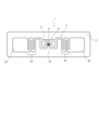
本発明の実施形態に係るRFIDインレイ1について説明する。図1は、本実施形態に係るRFIDインレイ1を説明する平面図である。
[RFID inlay]
An
図1に示されるように、RFIDインレイ1は、基材2と、基材2に金属箔により形成されたアンテナパターン3と、アンテナパターン3に接続されたICチップ4とを備える。
As shown in FIG. 1, the
<基材>
本実施形態において、基材2は、一例として、ポリ塩化ビニル、ポリエチレンテレフタレート、ポリプロピレン、ポリエチレン、ポリエチレンナフタレート等の樹脂フィルム単体又はこれら樹脂フィルムを複数積層してなる多層フィルムを使用することができる。
<Base material>
In the present embodiment, the
本実施形態においては、基材2として、上記樹脂フィルム基材のほか、上質紙、中質紙、又はこれらを用いて形成された塗工紙等の紙基材を用いることができる。
In this embodiment, as the
当該基材2上に形成されたアンテナパターン3に異方導電性材料を用いてICチップ4をマウントする際、ICチップ4と基材2との接着強度を高めることができることから、紙基材を使用することが好ましい。
When mounting the
基材2の厚さは、上記範囲内において、RFIDインレイ1を用いて作製される製品としてのRFID媒体の意匠性や用途等に応じて、適宜選択可能である。
The thickness of the
<アンテナパターン>
図1に示されるように、アンテナパターン3は、ループ部31と、ICチップ4がマウントされるICチップ接続部32と、ループ部31から左右対称に延びるメアンダ33,34と、メアンダ33,34の端部に接続されるキャパシタハット35,36とを備える。すなわち、アンテナパターン3は、ダイポールアンテナを構成する。
<Antenna pattern>
As shown in FIG. 1, the
本実施形態では、アンテナパターン3は、一例として、UHF帯(300MHz~3GHz、特に860MHz~960MHz)に対応したアンテナ長さ及びアンテナ線幅になるように設計されている。
In the present embodiment, the
また、本実施形態では、アンテナパターン3は、図示しないが、アクリル系粘着剤、ウレタン系粘着剤、シリコーン系粘着剤、ゴム系粘着剤等の粘着剤により基材2に接着されている。
Further, in this embodiment, although not shown, the
アンテナパターン3は、金属箔で形成されている。アンテナパターン3に適用可能な金属としては、例えば、銅、アルミニウムがあげられる。製造コストを抑える観点から、アルミニウム泊を用いることが好ましい。
The
RFIDインレイ1の全体の厚さ、RFID媒体に成型された際のRFID媒体全体の厚さ、及び製造コスト等の観点から、金属箔の厚さは、3μm以上25μm以下であることが好ましい。本実施形態においては、一例として、厚さ20μmのアルミニウム箔が使用される。
From the viewpoints of the overall thickness of the
<ICチップ>
RFIDインレイ1において、ICチップ4は、UHF帯に対応して、ICチップ4の読取装置であるリーダ(図示されていない)との間で通信可能に設計された半導体パッケージである。
<IC chip>
In the
ICチップ4は、アンテナパターン3のループ部31の一部に形成されたICチップ接続部32に、異方導電性接着剤、異方導電性フィルム等の異方導電性材料E(図3に示される)によって電気的及び機械的に接続される。
The
異方導電性材料Eは、接着成分であるバインダ樹脂中に、所定粒径に調製された導電性フィラーが混合されたものであり、熱圧着又は紫外線硬化等の処理により、アンテナパターン3とICチップ4とを電気的及び機械的に接続することができる。
The anisotropically conductive material E is a mixture of a conductive filler adjusted to a predetermined particle size in a binder resin as an adhesive component, and is bonded to the
[アンテナパターンにおけるICチップ接続部の構成]
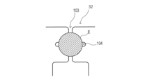
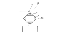
続いて、アンテナパターン3におけるICチップ接続部32について説明する。図2は、アンテナパターン3におけるICチップ接続部32を含む要部S(図1参照)を拡大して示す拡大図である。
[Configuration of IC chip connection part in antenna pattern]
Next, the IC
ICチップ接続部32には、ICチップ4に形成されたバンプ(図示されていない)と電気的に接続するための一対の接点(以下、バンプ接点と記す)101,102が形成されている。
A pair of contacts (hereinafter referred to as bump contacts) 101 and 102 are formed on the IC
ICチップ接続部32は、第一スリット103と第二スリット104とを有する。第一スリット103は、一対のバンプ接点101,102の間(図1に示すY方向)に沿って形成されている。また、第二スリット104は、バンプ接点101,102の並ぶ方向(図1に示すX方向)に沿って、第一スリット103に交差して形成されている。
The IC
ここで、第一スリット103と第二スリット104との交差部分Cにおいて、アンテナパターン3にできる4つの角部を、以下、角部P1,P2,P3,P4と称する。
Here, the four corners formed in the
図2において、異方導電性材料Eが配置される領域SEは、一点鎖線で示されている。また、ICチップ4が配置される領域SCは、二点鎖線で示されている。
In FIG. 2, the region SE where the anisotropically conductive material E is arranged is indicated by a chain line. Further, the area SC where the
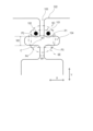
図3は、本実施形態に係るRFIDインレイ1において、アンテナパターン3にICチップ4を接合する工程を説明する模式図である。図3(a)に示されるように、異方導電性材料Eは、第一スリット103及び第二スリット104の交差部分Cを含む位置に充填されるとともに、バンプ接点101,102を含むアンテナパターン3(ICチップ接続部32)の表面に配置される。
FIG. 3 is a schematic diagram illustrating the process of bonding the
また、図3(b)に示されるように、ICチップ4は、アンテナパターン3の角部P1,P2,P3及びP4に支持される位置に合わせて配置される。また、第一スリット103及び第二スリットの交差部分Cに充填されるとともに、バンプ接点101,102を含むアンテナパターン3表面に配置された異方導電性材料Eによって、アンテナパターン3と基材2とに電気的及び機械的に接続される。
Further, as shown in FIG. 3(b), the
これにより、ICチップ4は、交差部分Cに充填された状態で固化した異方導電性材料Eによって、基材2のX方向及びY方向の二軸方向においてアンテナパターン3と基材2とに接着される。
As a result, the
また、図2に示すように、交差部分Cにおいて、第二スリット104を挟んで、バンプ接点101,102と対向する側のICチップ接続部32の角部P3及びP4には、曲線部分Rが形成されている。角部P3,P4に曲線部分Rが形成されることにより、交差部分Cの面積が広げられる。このため、交差部分Cにおいて、異方導電性材料Eが充填される領域を拡張することができる。
In addition, as shown in FIG. 2, at the intersection C, curved portions R are formed at corners P3 and P4 of the IC
また、本実施形態において、特に、基材2が紙基材である場合には、異方導電性材料Eのバインダ樹脂が紙基材に浸潤することができる。このため、ICチップ4と基材2との接着が強固になる。
Moreover, in this embodiment, especially when the
以上の構成を有するRFIDインレイ1は、表面や裏面に別の基材を積層したり、粘着剤層を形成したりするなどのさらなる加工が施されることにより、ラベル、タグ、リストバンド、チケット、カード等のRFID媒体を形成することができる。
The
<効果>
本実施形態に係るRFIDインレイ1によれば、ICチップ接続部32に、一対のバンプ接点101,102の間を通って(Y方向)形成された第一スリット103と、バンプ接点101,102の並ぶ方向(X方向)に沿って第一スリット103に交差して形成された第二スリット104とを有する。
<Effect>
According to the
そして、ICチップ4は、アンテナパターン3の角部P1,P2,P3及びP4に支持されるとともに、第一スリット103と第二スリット104との交差部分C、及びバンプ接点101,102を含むアンテナパターン3(ICチップ接続部32)の表面に配置された異方導電性材料Eによって、アンテナパターン3と基材2とに電気的及び機械的に接続されている。
The
本実施形態においては、ICチップ4は、アンテナパターン3の角部P1,P2,P3及びP4に支持されるため、アンテナパターン3に対する水平度を保持して安定して、アンテナパターン3に接続することができる。
In this embodiment, since the
また、ICチップ接続部32に第一スリット103及び第二スリット104が形成されていることにより、ICチップ4が基材2のX方向及びY方向の二軸方向において、異方導電性材料Eによってアンテナパターン3と基材2とに接着される。
Furthermore, since the
これにより、従来、バンプ間に形成された第一スリットに配置された異方導電性材料Eの接着力に頼ってICチップ4をアンテナパターン3に接続していた方法に比べて、ICチップ4と基材2とをX方向及びY方向の二軸方向に働く接着力によって支持することができる。
As a result, the
したがって、温度変化によるアンテナパターン3の収縮に伴う変形や、RFIDインレイ1のX方向及びY方向への曲げに対する耐久性を高めることができる。
Therefore, the durability against deformation due to shrinkage of the
また、交差部分Cにおいて、ICチップ接続部32の角部P3及びP4には、曲線部分Rが形成されている。このため、交差部分Cにおいて、異方導電性材料Eが充填される領域を拡張することができる。したがって、異方導電性材料Eと基材2との接着面積を広くすることができ、ICチップ4と基材2との接着強度を高めることができる。
Furthermore, at the intersection C, curved portions R are formed at corners P3 and P4 of the IC
図2に示したRFIDインレイ1においては、角部P1,P2にも、曲線部分Rが形成されていてもよい。この場合には、角部P3,P4に曲線部分Rを形成した場合と同様に、交差部分Cに異方導電性材料Eが充填される領域を拡張することができる。
In the
RFIDインレイ1においては、少なくともICチップ接続部32の角部P3及びP4に曲線部分Rが形成されていることで、ICチップ4と基材2との接着強度を高める効果が得られる。
In the
本実施形態において、基材2が紙基材である場合には、異方導電性材料Eのバインダ樹脂を紙基材に浸潤させることができる。このため、ICチップ4は、基材2(紙基材)に浸潤した異方導電性材料Eによって、基材2(紙基材)との間で強固に接着される。したがって、ICチップ4とアンテナパターン3との機械的接続を高めることができる。
In this embodiment, when the
[ICチップ接続部の変形例]
<第一変形例>
図4は、本実施形態の第一変形例を説明する平面図である。図4には、第一変形例として示すICチップ接続部321の要部が拡大して示されている。なお、第一変形例において、上述した実施形態と同様の作用効果を有する構成には同一の番号を付して詳細な説明は省略する。
[Modified example of IC chip connection part]
<First modification example>
FIG. 4 is a plan view illustrating a first modification of this embodiment. FIG. 4 shows an enlarged view of a main part of an IC
ICチップ接続部321では、第二スリット104を挟んで、バンプ接点101,102と対向する側における第一スリット103の幅W11が、バンプ接点101,102側における第一スリット103の幅W12よりも広く形成されている。
In the IC
ただし、第一スリット103の幅W11は、角部P3,P4においてICチップ4を安定して支持可能な面積が残されるような幅に設定されている。
However, the width W11 of the
上記構成により、第一変形例では、アンテナパターン3に対する水平度を保持しつつ、ICチップ4を安定してアンテナパターン3に接続することができる。
With the above configuration, in the first modification, the
また、ICチップ接続部321の角部P3及びP4のX方向の間隔が広がっているため、交差部分Cに異方導電性材料Eが充填される領域を拡張することができる。したがって、異方導電性材料Eと基材2との接着面積を広くすることができ、ICチップ4と基材2との接着強度を高めることができる。
Further, since the distance between the corner portions P3 and P4 of the IC
特に、基材2が紙基材である場合には、異方導電性材料Eのバインダ樹脂を紙基材に浸潤させることのできる面積が広がるため、ICチップ4と基材2(紙基材)との間における接着強度を一層高めることができる。
In particular, when the
<第二変形例>
図5は、本実施形態の第二変形例を説明する平面図である。図5には、第二変形例として示すICチップ接続部322の要部が拡大して示されている。なお、第二変形例において、上述した実施形態と同様の作用効果を有する構成には同一の番号を付して詳細な説明は省略する。
<Second modification example>
FIG. 5 is a plan view illustrating a second modified example of this embodiment. FIG. 5 shows an enlarged view of a main part of an IC
ICチップ接続部322では、第二スリット104の幅W2が第一スリット103の幅W1よりも広く形成されている。
In the IC
ただし、第二スリット104の幅W2は、角部P1とP3、及び角部P2とP4においてICチップ4を安定して支持可能な面積が残されるような幅に設定されている。
However, the width W2 of the
上記構成により、第二変形例では、アンテナパターン3に対する水平度を保持しつつ、ICチップ4を安定してアンテナパターン3に接続することができる。
With the above configuration, in the second modification, the
また、第二変形例では、ICチップ接続部32の角部P1とP3、及び角部P2とP4のY方向の間隔が広がっているため、交差部分Cに異方導電性材料Eが充填される領域を拡張することができる。したがって、異方導電性材料Eと基材2との接着面積を広くすることができ、ICチップ4と基材2との接着強度を高めることができる。
In addition, in the second modification, since the distance in the Y direction between the corners P1 and P3 and the corners P2 and P4 of the IC
特に、基材2が紙基材である場合には、異方導電性材料Eのバインダ樹脂を紙基材に浸潤させることのできる面積が広がるため、ICチップ4と基材2(紙基材)との間における接着強度を一層高めることができる。
In particular, when the
<第三変形例>
図6は、本実施形態の第三変形例を説明する平面図である。図6には、第三変形例として示すICチップ接続部323の要部が拡大して示されている。なお、第三変形例において、上述した実施形態と同様の作用効果を有する構成には同一の番号を付して詳細な説明は省略する。
<Third modification example>
FIG. 6 is a plan view illustrating a third modification of this embodiment. FIG. 6 shows an enlarged view of a main part of an IC
ICチップ接続部323では、交差部分Cが、角部P1,P2において、少なくともバンプ接点101,102を形成可能な領域が残される位置まで拡張されている。すなわち、角部P1,P2が曲線加工されて、バンプ接点101,102近傍まで減じられている。
In the IC
また、角部P3,P4は削減されて、代わりに、ICチップ4の隅を支持可能な支持領域Q1,Q2が残される位置まで、交差部分Cが拡張されている。
Furthermore, the corner portions P3 and P4 are reduced, and the intersection C is expanded to a position where supporting regions Q1 and Q2 capable of supporting the corners of the
上記構成により、第三変形例では、角部P1,P2及び支持領域Q1,Q2において、アンテナパターン3に対するICチップ4の水平度を保持しつつ、異方導電性材料Eと基材2との接着面積を最大限に広くしているため、ICチップ4を安定してアンテナパターン3に接続することができる。これにより、ICチップ4と基材2との接着強度を高めることができる。
With the above configuration, in the third modification, the horizontality of the
特に、基材2が紙基材である場合には、異方導電性材料Eのバインダ樹脂を紙基材に浸潤させることのできる面積が広がるため、ICチップ4と基材2(紙基材)との間における接着強度を一層高めることができる。
In particular, when the
[その他の実施形態]
以上、本発明の実施形態について説明したが、上記実施形態は、本発明の適用例の一部を示したに過ぎず、本発明の技術的範囲を上記実施形態の具体的構成に限定する趣旨ではない。
[Other embodiments]
Although the embodiments of the present invention have been described above, the above embodiments merely show a part of the application examples of the present invention, and the purpose is to limit the technical scope of the present invention to the specific configuration of the above embodiments. isn't it.
本実施形態においては、アンテナパターン3がUHF帯インレット用のダイポールアンテナである場合について説明したが、HF帯用のコイルアンテナであってもよい。
In this embodiment, a case has been described in which the
図4及び図5に示したRFIDインレイにおいても、角部P1,P2にも、曲線部分Rが形成されていてもよい。この場合には、角部P3,P4に曲線部分Rを形成した場合と同様に、交差部分Cに異方導電性材料Eが充填される領域を拡張することができる。したがって、異方導電性材料Eと基材2との接着面積を広くすることができ、ICチップ4と基材2との接着強度を高めることができる。
In the RFID inlay shown in FIGS. 4 and 5, curved portions R may also be formed at the corners P1 and P2. In this case, similarly to the case where the curved portions R are formed at the corners P3 and P4, it is possible to expand the area in which the intersecting portion C is filled with the anisotropically conductive material E. Therefore, the adhesive area between the anisotropic conductive material E and the
異方導電性材料Eとしては、異方導電性接着剤のほか異方導電性フィルムを使用することができる。異方導電性フィルムは、上述したフィラー及びバインダが樹脂シートに固定されたものであり、熱圧着により用いられる。異方導電性材料Eは、熱硬化型であっても、紫外線硬化型であってもよい。 As the anisotropically conductive material E, an anisotropically conductive film can be used in addition to an anisotropically conductive adhesive. The anisotropic conductive film is a film in which the filler and binder described above are fixed to a resin sheet, and is used by thermocompression bonding. The anisotropically conductive material E may be of a thermosetting type or an ultraviolet curing type.
以下、実施例及び比較例により本発明をさらに詳細に説明するが、本発明はこれら実施例に限定されるものではない。 EXAMPLES Hereinafter, the present invention will be explained in more detail with reference to Examples and Comparative Examples, but the present invention is not limited to these Examples.
[ICチップの接着強度の評価]
実施例及び比較例の供試体としてのRFIDインレイを用意し、アンテナパターンに対するICチップの接着強度を、DieShear試験により評価した。
[Evaluation of adhesive strength of IC chip]
RFID inlays were prepared as specimens of Examples and Comparative Examples, and the adhesive strength of the IC chip to the antenna pattern was evaluated by a DieShear test.
DieShear試験は、以下の通りである。 The DieShear test is as follows.
図1を用いて説明したRFIDインレイ1に基づいて供試体を作成し、供試体としてのRFIDインレイ1の、ICチップ4の側面に規定の治具(剥離爪)を押し当てて、基材2の平面に沿う方向に負荷をかけ、ICチップ4がアンテナパターン3から剥離したときの印加荷重を測定した。なお、基材2の平面において、負荷方向として、X方向とY方向のそれぞれについて測定した。
A specimen is created based on the
<実施例1>
・基材:紙(厚さ80μm)
・アンテナ:アルミニウム箔(厚さ20μm)
ライン幅:30μm~40μm、ライン深さ:1μm~2μm
ライン間隔:50μm~60μm
・異方導電性材料:紫外線硬化型異方導電性接着剤
・ICチップタイプ:IMPINJ社製 MONZA R6
・異方導電性材料の硬化条件:温度(室温25℃)、UV照射(3000mJ/cm2~5000mJ/cm2)、照射時間(3秒)、加圧(圧力1.0N)
・アンテナパターン
第一スリット幅:0.2mm
第二スリット幅:0.2mm
<Example 1>
・Base material: Paper (thickness 80μm)
・Antenna: Aluminum foil (thickness 20μm)
Line width: 30μm to 40μm, line depth: 1μm to 2μm
Line spacing: 50μm~60μm
・Anisotropic conductive material: UV-curable anisotropic conductive adhesive ・IC chip type: MONZA R6 manufactured by IMPINJ
・Curing conditions for anisotropic conductive material: temperature (room temperature 25°C), UV irradiation (3000mJ/cm 2 - 5000mJ/cm 2 ), irradiation time (3 seconds), pressure (pressure 1.0N)
・Antenna pattern First slit width: 0.2mm
Second slit width: 0.2mm
<比較例1>
比較例1の供試体は、第二スリット104が形成されていないアンテナパターンを使用した以外は、実施例1と同条件にて作製した。
<Comparative example 1>
The specimen of Comparative Example 1 was manufactured under the same conditions as Example 1, except that an antenna pattern in which the
<評価結果>
アンテナパターン3とアンテナパターン3に実装されたICチップ4との接着強度をDieShear試験によって評価した。ICチップ4がアンテナパターン3から剥離したときの印加荷重は、各供試体について、同条件で5回の試験を行った結果の平均値で表される。結果を第1表に示す。
<Evaluation results>
The adhesive strength between the

第1表に示されるように、比較例1と実施例1とを比べると、第二スリットが形成された実施例1では、同じ異方導電性接着剤を使用して同じ条件で接着した比較例のRFIDインレイと比べて、負荷荷重が印加された方向における耐久荷重の差が小さいことがわかった。 As shown in Table 1, when Comparative Example 1 and Example 1 are compared, Example 1 in which the second slit was formed was compared with the one in which the same anisotropic conductive adhesive was used and bonded under the same conditions. Compared to the RFID inlay in the example, it was found that the difference in the durable load in the direction in which the applied load was applied was small.
また、実施例1のRFIDインレイ1は、比較例のRFIDインレイに比べて、アンテナパターン3からICチップ4が剥離したときの印加荷重が、Y方向において11.3%、X方向において21.9%向上することが明らかとなった。
In addition, in the
1 RFIDインレイ
2 基材
3 アンテナパターン
4 ICチップ
31 ループ部
32 ICチップ接続部
33,34 メアンダ
35,36 キャパシタハット
101,102 バンプ接点
103 第一スリット
104 第二スリット
321 ICチップ接続部
322 ICチップ接続部
323 ICチップ接続部
C 交差部分
E 異方導電性材料
P1,P2,P3,P4 角部
Q1,Q2 支持領域
R 曲線部分
SE 領域(異方導電性材料Eが配置される領域)
SC 領域(ICチップ4が配置される領域)
1
SC area (area where
Claims (7)
前記アンテナパターンは、ダイポールアンテナを構成し、
前記ICチップとの一対の接点の間を通って形成され、前記一対の接点の間において前記ダイポールアンテナを分離する第一スリットと、
前記一対の接点の並ぶ方向に沿って前記第一スリットに交差し、前記一対の接点の並ぶ方向に沿って前記ダイポールアンテナを分離させることなく部分的に形成された第二スリットと、を備え、
前記ICチップが、前記第一スリット及び前記第二スリットの交差部分を含む位置に充填されるとともに前記一対の接点を含む前記アンテナパターンの表面に配置された異方導電性材料によって、前記アンテナパターンに接続された、
RFIDインレイ。 An RFID inlay comprising a base material, an antenna pattern formed on the base material, and an IC chip connected to the antenna pattern,
the antenna pattern constitutes a dipole antenna;
a first slit formed between a pair of contacts with the IC chip and separating the dipole antenna between the pair of contacts ;
a second slit that intersects the first slit along the direction in which the pair of contacts are arranged and is partially formed without separating the dipole antenna along the direction in which the pair of contacts are arranged ;
The IC chip is filled in a position including the intersection of the first slit and the second slit, and the antenna pattern is formed by an anisotropic conductive material disposed on the surface of the antenna pattern including the pair of contacts. connected to,
RFID inlay.
前記交差部分において、少なくとも、前記第二スリットを挟んで、前記一対の接点と対向する側の前記アンテナパターンの角部に曲線部分が形成された、
RFIDインレイ。 RFID inlay according to claim 1,
At the intersection, a curved portion is formed at least at a corner of the antenna pattern on the side opposite to the pair of contacts across the second slit.
RFID inlay.
前記第二スリットを挟んで、前記一対の接点と対向する側の前記第一スリットにおける幅は、他方側の幅よりも広い、
RFIDインレイ。 RFID inlay according to claim 1 or 2,
The width of the first slit on the side facing the pair of contacts across the second slit is wider than the width on the other side.
RFID inlay.
前記第二スリットの幅は、前記第一スリットの幅よりも広い、
RFIDインレイ。 RFID inlay according to claim 1 or 2,
The width of the second slit is wider than the width of the first slit.
RFID inlay.
前記基材が紙基材である、
RFIDインレイ。 RFID inlay according to any one of claims 1 to 4,
the base material is a paper base material,
RFID inlay.
前記アンテナパターンは、
前記ICチップとの一対の接点の間を通って形成された第一スリットと、
前記一対の接点の並ぶ方向に沿って前記第一スリットに交差して形成された第二スリットと、を備え、
前記ICチップが、前記第一スリット及び前記第二スリットの交差部分を含む位置に充填されるとともに前記一対の接点を含む前記アンテナパターンの表面に配置された異方導電性材料によって、前記アンテナパターンに接続され、
前記交差部分において、少なくとも、前記第二スリットを挟んで、前記一対の接点と対向する側の前記アンテナパターンの角部に曲線部分が形成された、
RFIDインレイ。 An RFID inlay comprising a base material, an antenna pattern formed on the base material, and an IC chip connected to the antenna pattern,
The antenna pattern is
a first slit formed through a pair of contact points with the IC chip;
a second slit formed to intersect the first slit along the direction in which the pair of contacts are lined up;
The IC chip is filled in a position including the intersection of the first slit and the second slit, and the antenna pattern is formed by an anisotropic conductive material disposed on the surface of the antenna pattern including the pair of contacts. connected to,
At the intersection, a curved portion is formed at least at a corner of the antenna pattern on the side opposite to the pair of contacts across the second slit.
RFID inlay.
前記アンテナパターンは、
前記ICチップとの一対の接点の間を通って形成された第一スリットと、
前記一対の接点の並ぶ方向に沿って前記第一スリットに交差して形成された第二スリットと、を備え、
前記ICチップが、前記第一スリット及び前記第二スリットの交差部分を含む位置に充填されるとともに前記一対の接点を含む前記アンテナパターンの表面に配置された異方導電性材料によって、前記アンテナパターンに接続され、
前記第二スリットを挟んで、前記一対の接点と対向する側の前記第一スリットにおける幅は、他方側の幅よりも広い、
RFIDインレイ。 An RFID inlay comprising a base material, an antenna pattern formed on the base material, and an IC chip connected to the antenna pattern,
The antenna pattern is
a first slit formed through a pair of contact points with the IC chip;
a second slit formed to intersect the first slit along the direction in which the pair of contacts are lined up;
The IC chip is filled in a position including the intersection of the first slit and the second slit, and the antenna pattern is formed by an anisotropic conductive material disposed on the surface of the antenna pattern including the pair of contacts. connected to,
The width of the first slit on the side facing the pair of contacts across the second slit is wider than the width on the other side.
RFID inlay.
Priority Applications (2)
| Application Number | Priority Date | Filing Date | Title |
|---|---|---|---|
| JP2020040124A JP7451237B2 (en) | 2020-03-09 | 2020-03-09 | RFID inlay |
| JP2024033920A JP7620748B2 (en) | 2020-03-09 | 2024-03-06 | RFID Inlay |
Applications Claiming Priority (1)
| Application Number | Priority Date | Filing Date | Title |
|---|---|---|---|
| JP2020040124A JP7451237B2 (en) | 2020-03-09 | 2020-03-09 | RFID inlay |
Related Child Applications (1)
| Application Number | Title | Priority Date | Filing Date |
|---|---|---|---|
| JP2024033920A Division JP7620748B2 (en) | 2020-03-09 | 2024-03-06 | RFID Inlay |
Publications (2)
| Publication Number | Publication Date |
|---|---|
| JP2021140671A JP2021140671A (en) | 2021-09-16 |
| JP7451237B2 true JP7451237B2 (en) | 2024-03-18 |
Family
ID=77669650
Family Applications (2)
| Application Number | Title | Priority Date | Filing Date |
|---|---|---|---|
| JP2020040124A Active JP7451237B2 (en) | 2020-03-09 | 2020-03-09 | RFID inlay |
| JP2024033920A Active JP7620748B2 (en) | 2020-03-09 | 2024-03-06 | RFID Inlay |
Family Applications After (1)
| Application Number | Title | Priority Date | Filing Date |
|---|---|---|---|
| JP2024033920A Active JP7620748B2 (en) | 2020-03-09 | 2024-03-06 | RFID Inlay |
Country Status (1)
| Country | Link |
|---|---|
| JP (2) | JP7451237B2 (en) |
Citations (3)
| Publication number | Priority date | Publication date | Assignee | Title |
|---|---|---|---|---|
| JP2010015342A (en) | 2008-07-03 | 2010-01-21 | Dainippon Printing Co Ltd | Antenna sheet, inlet, and ic tag |
| JP2015108933A (en) | 2013-12-04 | 2015-06-11 | 日立化成株式会社 | Noncontact ic card |
| JP2021096540A (en) | 2019-12-13 | 2021-06-24 | 日本パッケージ・システム株式会社 | Rfid inlay and manufacturing method thereof |
Family Cites Families (1)
| Publication number | Priority date | Publication date | Assignee | Title |
|---|---|---|---|---|
| JP4322558B2 (en) * | 2003-05-30 | 2009-09-02 | 株式会社ルネサステクノロジ | Method for manufacturing inlet for electronic tag |
-
2020
- 2020-03-09 JP JP2020040124A patent/JP7451237B2/en active Active
-
2024
- 2024-03-06 JP JP2024033920A patent/JP7620748B2/en active Active
Patent Citations (3)
| Publication number | Priority date | Publication date | Assignee | Title |
|---|---|---|---|---|
| JP2010015342A (en) | 2008-07-03 | 2010-01-21 | Dainippon Printing Co Ltd | Antenna sheet, inlet, and ic tag |
| JP2015108933A (en) | 2013-12-04 | 2015-06-11 | 日立化成株式会社 | Noncontact ic card |
| JP2021096540A (en) | 2019-12-13 | 2021-06-24 | 日本パッケージ・システム株式会社 | Rfid inlay and manufacturing method thereof |
Also Published As
| Publication number | Publication date |
|---|---|
| JP7620748B2 (en) | 2025-01-23 |
| JP2024056008A (en) | 2024-04-19 |
| JP2021140671A (en) | 2021-09-16 |
Similar Documents
| Publication | Publication Date | Title |
|---|---|---|
| JP4052111B2 (en) | Wireless information storage medium | |
| AU742212B2 (en) | Card mounted with circuit chip and circuit chip module | |
| US7954722B2 (en) | IC tag and inlet for IC tag | |
| US20110011939A1 (en) | Contact-less and dual interface inlays and methods for producing the same | |
| EP2245578B1 (en) | Rfid devices and methods for overlapped objects | |
| KR101897944B1 (en) | Method for Embedding an Integrated Circuit Flip Chip | |
| CN103797498B (en) | RFID tags and automatic identification systems | |
| CN101156164B (en) | Noncontact information storage medium and method for manufacturing same | |
| CN114586041A (en) | Rotation-insensitive RFID device and method of forming the same | |
| US20080164326A1 (en) | Connecting Part For Mounting IC Chip, Antenna Circuit, IC Inlet, IC Tag and Method of Adjusting Capacitance | |
| TWI284842B (en) | Communication medium capable of carrying out contactless communication and method of producing the same | |
| CN104978595A (en) | Dual interface IC card components and method for manufacturing dual-interface IC card components | |
| JP4176244B2 (en) | Chip card | |
| CN108701248B (en) | Circuit layer of integrated circuit card | |
| JP2010267150A (en) | Non-contact information recording medium | |
| JP7451237B2 (en) | RFID inlay | |
| CN117015782A (en) | Method for manufacturing a plurality of chip card modules and a strip of flexible material supporting the plurality of modules | |
| JP2000137781A (en) | Card type electronic circuit board and method of manufacturing the same | |
| JP4743369B2 (en) | Auxiliary antenna member for non-contact type data carrier device and article provided with the auxiliary antenna member | |
| JP4839828B2 (en) | Non-contact data carrier device for metal | |
| US20240419933A1 (en) | Leadframeless contactless module | |
| JP5548059B2 (en) | Circuit element | |
| JP4713942B2 (en) | Antenna member and non-contact type IC card using the same | |
| JP2002304608A (en) | Non-contact IC card | |
| JP2001005929A (en) | IC card |
Legal Events
| Date | Code | Title | Description |
|---|---|---|---|
| A621 | Written request for application examination |
Free format text: JAPANESE INTERMEDIATE CODE: A621 Effective date: 20230210 |
|
| A131 | Notification of reasons for refusal |
Free format text: JAPANESE INTERMEDIATE CODE: A131 Effective date: 20231128 |
|
| A977 | Report on retrieval |
Free format text: JAPANESE INTERMEDIATE CODE: A971007 Effective date: 20231130 |
|
| A521 | Request for written amendment filed |
Free format text: JAPANESE INTERMEDIATE CODE: A523 Effective date: 20240125 |
|
| TRDD | Decision of grant or rejection written | ||
| A01 | Written decision to grant a patent or to grant a registration (utility model) |
Free format text: JAPANESE INTERMEDIATE CODE: A01 Effective date: 20240206 |
|
| A61 | First payment of annual fees (during grant procedure) |
Free format text: JAPANESE INTERMEDIATE CODE: A61 Effective date: 20240306 |
|
| R150 | Certificate of patent or registration of utility model |
Ref document number: 7451237 Country of ref document: JP Free format text: JAPANESE INTERMEDIATE CODE: R150 |