JP7413232B2 - Partial pressure device - Google Patents
Partial pressure device Download PDFInfo
- Publication number
- JP7413232B2 JP7413232B2 JP2020184549A JP2020184549A JP7413232B2 JP 7413232 B2 JP7413232 B2 JP 7413232B2 JP 2020184549 A JP2020184549 A JP 2020184549A JP 2020184549 A JP2020184549 A JP 2020184549A JP 7413232 B2 JP7413232 B2 JP 7413232B2
- Authority
- JP
- Japan
- Prior art keywords
- circuit
- gate
- signal
- daisy chain
- state
- Prior art date
- Legal status (The legal status is an assumption and is not a legal conclusion. Google has not performed a legal analysis and makes no representation as to the accuracy of the status listed.)
- Active
Links
Images


Landscapes
- Dc-Dc Converters (AREA)
Description
本発明の実施形態は、分圧装置に関する。 Embodiments of the present invention relate to a partial pressure device.
従来、複数の蓄電部を接続して構成されるスイッチトキャパシタが種々の用途に用いられている。スイッチトキャパシタは、高圧の直流電圧を生成して負荷に供給したり、高圧を分圧した電圧を用いて電圧調整を行うといった形で利用される。後者に関して従来の技術では、放電時において、負荷に接続される出力端子に至るまでに経由する蓄電部が多いことで、エネルギー効率が悪くなるという課題があった。 Conventionally, switched capacitors configured by connecting a plurality of power storage units have been used for various purposes. Switched capacitors are used to generate high DC voltage and supply it to a load, or to adjust voltage using a divided high voltage. Regarding the latter, conventional technology has a problem in that during discharging, there are many power storage units to pass through before reaching the output terminal connected to the load, resulting in poor energy efficiency.
本発明が解決しようとする課題は、エネルギー効率を高めることができる分圧装置を提供することである。 The problem to be solved by the present invention is to provide a partial pressure device that can improve energy efficiency.
実施形態の分圧装置は、第1回路と、第2回路とを持つ。第1回路は、複数の蓄電部を有する第2回路の入力端子に第1電圧を印加する。第2回路は、前記複数の蓄電部、および、前記複数の蓄電部の接続状態を、入力端子に対して直列に接続される第1状態と、出力端子に対して並列に接続される第2状態とのいずれかに少なくとも設定可能な接続回路を有する。前記第1回路は、前記複数の蓄電部の接続状態が前記第1状態であるときに、前記第2回路の入力端子に前記第1電圧を印加する。 The voltage dividing device of the embodiment has a first circuit and a second circuit. The first circuit applies a first voltage to an input terminal of a second circuit having a plurality of power storage units. The second circuit changes the connection states of the plurality of power storage units and the plurality of power storage units into a first state in which they are connected in series to an input terminal and a second state in which they are connected in parallel to an output terminal. It has a connection circuit that can be set to at least one of the states. The first circuit applies the first voltage to the input terminal of the second circuit when the plurality of power storage units are in the first state.
以下、実施形態の分圧装置を、図面を参照して説明する。 Hereinafter, a partial pressure device according to an embodiment will be described with reference to the drawings.
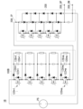
図1は、分圧装置1の基本構成図である。分圧装置1は、第1回路100と、第2回路200とを備える。第1回路100は、電力源PSに接続される。電力源PSは、一定電圧Vを供給する直流電源である。第1回路100は、第2回路200の入力端子200_IPに電圧V(第1電圧の一例)を印加する。第2回路200は、複数のコンデンサ(蓄電部)210#1~210#nと、接続回路(図1では不図示)とを有する。nは2以上の自然数である。接続回路は、複数のコンデンサ210#1~210#nの接続状態を、入力端子200_IPに対して直列に接続される第1状態と、出力端子200_OP、200_ONに対して並列に接続される第2状態と、のいずれかに少なくとも設定可能である。分圧装置1に充電電流や放電電流を制限する抵抗が付加されてもよい。
FIG. 1 is a basic configuration diagram of the
第1回路100は、複数コンデンサ210#1~210#nの接続状態が第1状態であるときに、第2回路200の入力端子200_IPに電圧Vを印加し、複数コンデンサ210#1~210#nの接続状態が第2状態であるときに、第2回路200の入力端子200_IPに電圧Vを印加しないように構成されている。以下、いずれのコンデンサであるかを区別しない場合は、単にコンデンサ210と称する場合がある。符号における「#1」~「#n」の部分は、どのコンデンサ210に対応するかを示すものであり、これについても適宜省略して説明する。各コンデンサ210として、例えば容量や特性が均一なコンデンサが用いられる。また、配置によって劣化のしやすさ等がばらつくことを考慮して、容量や特性が若干異なるコンデンサが各コンデンサ210として用いられてもよい。
The
分圧装置1は、第1回路100がオン状態であり且つ第2回路200が第1状態である状態と、第1回路100がオフ状態であり且つ第2回路200が第2状態である状態と、を交互に繰り返すことで、第2回路200の出力端子200_OP、200_ONから電圧V/n(第2電圧の一例)を継続的に供給する。なお第2回路200の出力端子200_OP、200_ONから供給される電圧には、状態の切り替わりに応じた若干の変動が生じる場合があるが、電圧を供給される側から見て誤差の範囲とみなされる程度の変動であれば許容されてよい。
The voltage dividing
第2回路200は、第1状態において、複数のコンデンサ210#1~210#nが入力電圧Vによって充電されると共に、コンデンサ210#nが出力端子200_OP、200_ONに電圧V/nを供給する。第2回路200は、第2状態において、各コンデンサ210#1~210#nから並列に、電圧V/nを供給する。係る構成および動作によって、第2回路200が第2状態の場合における、各コンデンサ210と出力端子200_OP、200_ONとの電気的距離が近くなるため、分圧装置1は、従来型のスイッチトキャパシタを用いた分圧装置に比してエネルギー効率を高めることができる。
In the
<第1実施形態>
図2は、第1実施形態に係る分圧装置1Aの構成図である。分圧装置1Aは、第1回路100Aと、第2回路200とを備える。以下、符号の数字の直後の大文字アルファベットは各実施形態に特有の構成を示し、大文字アルファベットが付されていない数字は各実施形態に共通の構成であるものとする。第1回路100Aは、例えば、IGBT(Insulated Gate Bipolar Transistor)110Aを含む。IGBT110Aのコレクタは電力源PSの正極側に、エミッタは第2回路200の入力端子200_IPにそれぞれ接続される。第1回路100Aは、IGBT110Aをオン状態にすることにより第2回路200の入力端子200_IPに電圧Vを印加し、IGBT110Aをオフ状態にすることにより第2回路200の入力端子200_IPに電圧を印加しない状態となる。
<First embodiment>
FIG. 2 is a configuration diagram of the pressure dividing device 1A according to the first embodiment. The voltage dividing device 1A includes a
第2回路200は、接続回路220を有する。接続回路220は、コンデンサ210#1~210#n-1のそれぞれに対応して、スイッチング素子222と、ダイオード224、226、および228とを有する(「#」以下の符号を省略)。図2では、コンデンサ210#1に関連するものと、コンデンサ210#n-1に関連するもののみを示している。以下、適宜「#」以下の符号を省略して説明する。
The
スイッチング素子222は、例えばMOSFET(Metal-Oxide-Semiconductor Field-Effect Transistor)である。スイッチング素子222のドレインは、コンデンサ210の正極に接続されており、スイッチング素子222のソースは、ダイオード226のカソード側に接続されている。ダイオード224はスイッチング素子222に対して逆並列に接続されているMOSFETの寄生ダイオードである。ダイオード226のアノードはコンデンサの負極側に接続されている。コンデンサ210とダイオード226の間の箇所と第2回路200の出力端子200_ONとの間は、ダイオード228によって電流方向が制限される一方向線路によって接続されている。以下、k=1~n-2として説明する。スイッチング素子222#kのソースは、スイッチング素子222#k+1のドレインに接続されている。。ダイオード226#kのカソードは、コンデンサ210#k+1の正極側に接続されている。
The switching
係る構成において、第1回路100AのIGBT110Aがオン状態のときに第2回路200のスイッチング素子222はオフ状態となるように制御され、第2回路200が第1状態となる。一方、第1回路100AのIGBT110Aがオフ状態のときに第2回路200のスイッチング素子222はオン状態となるように制御され、第2回路200が第2状態となる。IGBT110Aとスイッチング素子222は、同時にオン状態にならないように、状態切替の際に若干のタイムラグが設けられると好適である。
In such a configuration, when the
以上説明した第1実施形態によれば、従来型のスイッチトキャパシタを用いた分圧装置に比してエネルギー効率を高めることができる。 According to the first embodiment described above, energy efficiency can be improved compared to a voltage dividing device using a conventional switched capacitor.
<第2実施形態>
以下、第2実施形態について説明する。図3は、第2実施形態に係る分圧装置1Bの構成図である。分圧装置1Bは、例えば、第1回路100Bと、第2回路200とを備える。第2回路200は第1実施形態と同様であってよい。第1回路100Bは、例えば、互いに直列に接続された複数のスイッチング素子120*1~120*mを有する。mは2以上の自然数である。第1回路100Bは、スイッチング素子120*1~120*mのそれぞれに対応して、ダイオード122および124と、コンデンサ126と、抵抗器128とを有する(「*」以下の符号を省略)。図3では、スイッチング素子120*1に関連するものと、スイッチング素子120*mに関連するもののみを示している。以下、適宜「*」以下の符号を省略して説明する。本明細書における「抵抗器」は、線路が自然に有する抵抗を指すものであってよい。
<Second embodiment>
The second embodiment will be described below. FIG. 3 is a configuration diagram of a
スイッチング素子120は、例えばMOSFETである。スイッチング素子120のドレインは、ダイオード124を介してコンデンサ126の正極に接続されており、スイッチング素子120のソースは、コンデンサ126の負極に接続されている。ダイオード122はスイッチング素子120に対して逆並列に接続されているMOSFETの寄生ダイオードである。
The switching
係る構成において、第1回路100Bの全てのスイッチング素子120がオン状態のときに第2回路200のスイッチング素子222はオフ状態となるように制御され、第2回路200が第1状態となる。一方、第1回路100Aの全てのスイッチング素子120がオフ状態のときに第2回路200のスイッチング素子222はオン状態となるように制御され、第2回路200が第2状態となる。スイッチング素子120とスイッチング素子222は、同時にオン状態にならないように、状態切替の際に若干のタイムラグが設けられると好適である。
In such a configuration, when all the switching
このようにDRCスナバとして構成することで、スイッチング素子120がオンしたときに、コンデンサ126に蓄えられたエネルギーが全て損失にならない。
By configuring it as a DRC snubber in this manner, all of the energy stored in the
第2実施形態の比較例として、図3の構成からダイオード124、コンデンサ126および抵抗器128を省略したものと、図3の構成からダイオード124を省略したものが考えられる。前者においては、寄生容量や漏れ電流によって電圧がアンバランスになり、アバランシェまたは過電圧によってスイッチング素子120が故障する可能性がある。後者の場合、スイッチング素子120のターンオン時に損失が生じ、熱によって故障しやすくなるため、付設する冷却器を大きくしなければならない。第2実施形態の分圧装置1Bによれば、これらの不都合を抑制することができる。
As a comparative example of the second embodiment, there may be one in which the
<第3実施形態>
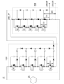
以下、第3実施形態について説明する。図4は、第3実施形態に係る分圧装置1Cの構成図である。分圧装置1Cは、例えば、第1回路100Cと、第2回路200とを備える。第2回路200は第1実施形態と同様であってよい。第3実施形態は、第1回路のスイッチング素子120のスナバを回生型にしたものである。
<Third embodiment>
The third embodiment will be described below. FIG. 4 is a configuration diagram of a
第1回路100Cは、スイッチング素子120*1~120*mのそれぞれに対応して、MOSFETの寄生ダイオード122、ダイオード130および134と、コンデンサ126と、抵抗器132とを有する(「*」以下の符号を省略)。図4では、スイッチング素子120*1に関連するものと、スイッチング素子120*mに関連するもののみを示している。以下、適宜「*」以下の符号を省略して説明する。
The
スイッチング素子120は、例えばMOSFETである。スイッチング素子120のドレインは、コンデンサ126の正極に接続されており、スイッチング素子120のソースは、ダイオード130を介してコンデンサ126の負極に接続されている。ダイオード122はスイッチング素子120に対して逆並列に接続されている。コンデンサ126とダイオード130の間の箇所と、第2回路200におけるダイオード228によって電流方向が制限される一方向線路との間は、ダイオード134によって電流方向が第2回路200の一方向線路と同じ方向に制限される一方向線路によって接続されている。抵抗器132は、この一方向線路に設けられている。
The switching
第2実施形態では、コンデンサ126に蓄えられたエネルギーは抵抗器128によって消費されるが、第3実施形態では、第2回路200のコンデンサ210によって回収される。このため、第3実施形態によれば、コンデンサ126に蓄えられたエネルギーを有効活用することができ、エネルギー効率を改善することができる。
In the second embodiment, the energy stored in
<第4実施形態>
以下、第4実施形態について説明する。第4実施形態の分圧装置1Dは、第2実施形態の分圧装置1Bまたは第3実施形態の分圧装置1Cにおいて、第1回路100Bまたは100Cと、第2回路200と、のうち一方または双方が有する複数のスイッチング素子を、一つのゲートドライバの動作によって波及的にオン状態またはオフ状態にするゲートデイジーチェーン回路を更に有するものである。図5は、第4実施形態に係る分圧装置1Dの構成図である。図5の例では、分圧装置1Dは、第1回路100Bまたは100Cを駆動する第1ゲートデイジーチェーン回路300(1)と、第2回路200を駆動する第2ゲートデイジーチェーン回路300(2)とを備える。以下、いずれのゲートデイジーチェーン回路であるかを区別せず、単にゲートデイジーチェーン回路300と称して説明する。
<Fourth embodiment>
The fourth embodiment will be described below. The
図6は、第4実施形態に係るゲートデイジーチェーン回路300の構成図である。ゲートデイジーチェーン回路300は、一段目の駆動回路310-1と、二段目以降の駆動回路310-q(q=2~nまたはm)とを備える。駆動回路310-1は、例えば、増幅器312と、抵抗器314および316と、ダイオード318とを有する。増幅器312には、ゲート電圧Vd-Vgndが常時印加されており、ゲート信号Vgが与えられる。増幅器312の出力電圧は、抵抗器314を介してスイッチング素子120または222のゲートに印加される。抵抗器316およびダイオード318は、抵抗器314と並列に設けられ、スイッチング素子120または222のゲートから増幅器312に流れる電流を選択的に許容する。
FIG. 6 is a configuration diagram of a gate
二段目以降の駆動回路310-qは、例えば、第1線路320と、第2線路322と、抵抗器324および328と、ダイオード326と、PNPバイポーラトランジスタ330とを有する。図6では、駆動回路310-2に関する構成のみ符号を示している。
The drive circuit 310-q in the second and subsequent stages includes, for example, a
第1線路320は、増幅器312の出力側からの電流を許容する一方向線路340と、スイッチング素子120または222のゲートとを接続する。第1線路320には、一方向線路340の側から順に、抵抗器324とダイオード326とが設けられる。第2線路322は、抵抗器324とダイオード326との間の箇所と、スイッチング素子120または222のソースとを接続する。第2線路322には、抵抗器328が設けられる。PNPバイポーラトランジスタ330のベースは、抵抗器324とダイオード326との間の箇所と接続され、エミッタは第1線路320と、コレクタは第2線路322とそれぞれ接続される。
The
係る構成において、増幅器312にゲート信号Vgが与えられると、一段目の駆動回路310-1、二段目の駆動回路310-2、三段目の駆動回路310-3…の順に、スイッチング素子120または222のゲートにHi信号を印加する。p段目の駆動回路310-pに対応するスイッチング素子120または222がオン状態になることで、p+1段目の駆動回路310-p+1に対応するスイッチング素子120または222のソース電位が、一段目の駆動回路310-1に対応するスイッチング素子120または222のソース電位と一致し、それによってp+1段目の駆動回路310-p+1に対応するスイッチング素子120または222のゲート―ソース間電圧がオン閾値を超えることでオン状態となる。この動作が波及的に生じることで、一つのゲート信号Vgで複数のスイッチング素子120または222が波及的にオン状態となる。
In such a configuration, when the gate signal Vg is applied to the
一方、増幅器312にゲート信号Vgを与えるのを停止すると、一段目の駆動回路310-1に対応するスイッチング素子120または222がオフ状態となる。それ以外のスイッチング素子120または222は、PNPバイポーラトランジスタ330のプルダウン抵抗(ベース抵抗)に流れる電流がPNPバイポーラトランジスタ330によって増幅されることで、オフ状態となる。プルダウン抵抗だけでもオフ状態にすることは可能であるが、増幅したほうがオン期間中の待機損失を低減することができる。なお、PNPバイポーラトランジスタ330をPチャネルのFETに置き換えることも可能だが、FETのオン閾値分だけ電荷が残るため、素子のゲートソース(ゲートエミッタ)間にプルダウン抵抗が必要となる。
On the other hand, when the application of the gate signal Vg to the
以上説明した第4実施形態によれば、一つのゲート信号Vgで複数のスイッチング素子120または222を波及的にオンオフすることができ、装置の小型化やコスト低減を実現することができる。
According to the fourth embodiment described above, it is possible to turn on and off a plurality of switching
<第5実施形態>
以下、第5実施形態について説明する。図7は、第5実施形態に係る分圧装置1Eの構成図である。分圧装置1Eは、第4実施形態の構成に加えて、ゲート信号発生装置400Eを備える。第5実施形態以降では、分圧装置が第1ゲートデイジーチェーン回路300(1)と第2ゲートデイジーチェーン回路300(2)とを備えることを前提とする。
<Fifth embodiment>
The fifth embodiment will be described below. FIG. 7 is a configuration diagram of a
図8は、第5実施形態に係るゲート信号発生装置400Eの構成図である。ゲート信号発生装置400Eは、例えば、PWM(Pulse Width Modulation)信号発生器402と、論理反転回路404と、信号絶縁回路406とを有する。PWM信号発生器402は、所定周期でHi信号とLo信号を繰り返し発生させる。論理反転回路404は、PWM信号発生器402による出力されたHi信号をLo信号に、Lo信号をHi信号にそれぞれ変換する(反転させる)。信号絶縁回路406は、ゲート信号発生装置400E、第1ゲートデイジーチェーン回路300(1)、および第2ゲートデイジーチェーン回路300(2)を介して第1回路100Bまたは100Cと第2回路200が導通しないように、電気的絶縁を確保する。信号絶縁回路406により出力された信号は第1ゲートデイジーチェーン回路300(1)に出力され、PWM信号発生器402により出力された信号は第2ゲートデイジーチェーン回路300(2)に出力される。あるいは、信号絶縁回路406により出力された信号は第2ゲートデイジーチェーン回路300(2)に出力され、PWM信号発生器402により出力された信号は第1ゲートデイジーチェーン回路300(1)に出力される。これによって、第1ゲートデイジーチェーン回路300(1)と第2ゲートデイジーチェーン回路300(2)とを好適に駆動することができる。
FIG. 8 is a configuration diagram of a gate
以上説明した第5実施形態によれば、第1ゲートデイジーチェーン回路300(1)と第2ゲートデイジーチェーン回路300(2)とを好適に駆動することができる。なお、第5実施形態において第1ゲートデイジーチェーン回路300(1)に与えられる信号と、第2ゲートデイジーチェーン回路300(2)に与えられる信号とを同時にHi信号にしないための工夫については説明を書略している。 According to the fifth embodiment described above, the first gate daisy chain circuit 300(1) and the second gate daisy chain circuit 300(2) can be suitably driven. Note that in the fifth embodiment, a method for preventing the signal given to the first gate daisy chain circuit 300(1) and the signal given to the second gate daisy chain circuit 300(2) from becoming Hi signals at the same time will be explained. is omitted.
<第6実施形態>
以下、第6実施形態について説明する。第5実施形態の構成では、第1回路100Bまたは100Cと第2回路200が扱う電圧が高い場合に、信号絶縁回路406の絶縁耐圧を高くしなければならないため、信号絶縁回路406のコストやサイズが増大し、ひいては分圧装置1Eが大型化するという課題が生じる。第6および第7実施形態では、第1ゲートデイジーチェーン回路300(1)に接続される部分と、第2ゲートデイジーチェーン回路300(2)に接続される部分とが信号の受け渡しをすることなく、PWM信号を反転させた信号を自己発生する。これによって、異なる電位にある制御回路間での信号の受け渡しが不要となり、高絶縁耐圧の信号絶縁IC(例えば、第5実施形態の信号絶縁回路406)が不要になることで安価になり、信頼性が向上する。また、信号受け渡し部分の空間・沿面距離が不要となる。
<Sixth embodiment>
The sixth embodiment will be described below. In the configuration of the fifth embodiment, when the voltage handled by the
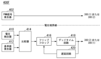
第6実施形態に係る分圧装置1Fは、第5実施形態の構成において、ゲート信号発生装置400Eに代えてゲート信号発生装置400Fを備える。図9は、第6実施形態に係るゲート信号発生装置400Fの構成図である。ゲート信号発生装置400Fは、PWM信号発生器402に加えて、電圧検出器410と、基準値発生器412と、比較器414と、フリップフロップ416と、デッドタイム回路418と、遅延回路420とを備える。PWM信号発生器402により出力された信号は第1ゲートデイジーチェーン回路300(1)に出力され、デッドタイム回路418により出力された信号は第2ゲートデイジーチェーン回路300(2)に出力される。或いは、PWM信号発生器402により出力された信号は第2ゲートデイジーチェーン回路300(2)に出力され、デッドタイム回路418により出力された信号は第1ゲートデイジーチェーン回路300(1)に出力される。以下の説明では前者であるものとする。本実施形態におけるPWM信号発生器402は、「第1信号供給部」の一例である。基準値発生器412、比較器414、フリップフロップ416、デッドタイム回路418、および遅延回路420を合わせたものが「第2信号供給部」の一例である。
A
電圧検出器410は、PWM信号発生器402により出力された信号に応じて第1ゲートデイジーチェーン回路300(1)が駆動されることで、第1回路100Bまたは100Cの所定の箇所に発生する電圧を検出する。図10は、電圧検出器410による電圧検出箇所の一例を示す図である。図中、(a)~(d)が電圧検出箇所となり得る箇所の例である。本図では、分圧装置1Fが第1回路100Cと第2回路200を備えるものとしている。
The
図11は、ゲート信号発生装置400Fの各部が出力する信号の時間的変化を比較したタイミングチャートである。PWM信号発生器402が出力するPWM信号は、一定周期でHiとLoが入れ替わる信号である。電圧検出器410の電圧検出値は、PWM信号とほぼ同様の波形を示し、そのため比較器414の出力はPWM信号とほぼ同じタイミングでHiとLoが入れ替わる信号となる。フリップフロップ416は、比較器414から入力される信号の立ち上がりに応じてオン状態(Hi信号を出力する状態)を維持し、遅延回路420からHi信号が入力される度にその状態をリセットする(Lo信号を出力する)ように動作する。デッドタイム回路418は、フリップフロップ416の出力する信号の立ち下りのタイミングから一定時間(デッドタイムの間)、Lo信号を出力し、それ以外の期間ではHi信号を出力する。遅延回路420は、デッドタイム回路418の出力する信号を、一定の位相だけ遅延させる。遅延回路420の遅延量は、遅延回路420の出力信号の立ち上がりがPWM信号の立ち上がりよりも若干早くなるように設定されている。また、デッドタイムはPWM信号の半周期よりも若干長い期間に設定されている。このため、第1ゲートデイジーチェーン回路300(1)に与えられるPWM信号と、第2ゲートデイジーチェーン回路300(2)に与えられるデッドタイム回路418の出力信号は、原則的に同時にHiにならないように制御される(後者が前者を反転した信号となる)と共に、切替期において同時にLoになる期間が設けられる。これによって、電力制御の効率性を維持しつつ意図しない故障等が生じるのを防止することができる。
FIG. 11 is a timing chart comparing temporal changes in signals output from each part of the gate
以上説明した第6実施形態によれば、第5実施形態に比して絶縁のためのコストやサイズを低減することができる。 According to the sixth embodiment described above, the cost and size for insulation can be reduced compared to the fifth embodiment.
(第7実施形態)
以下、第7実施形態について説明する。第7実施形態に係る分圧装置1Gは、第5実施形態の構成において、ゲート信号発生装置400Eに代えてゲート信号発生装置400Gを備える。図12は、第7実施形態に係るゲート信号発生装置400Gの構成図である。ゲート信号発生装置400Gは、PWM信号発生器402に加えて、電流検出器422と、基準値発生器412と、比較器414と、フリップフロップ416と、デッドタイム回路418と、遅延回路420とを備える。PWM信号発生器402により出力された信号は第1ゲートデイジーチェーン回路300(1)に出力され、デッドタイム回路418により出力された信号は第2ゲートデイジーチェーン回路300(2)に出力される。或いは、PWM信号発生器402により出力された信号は第2ゲートデイジーチェーン回路300(2)に出力され、デッドタイム回路418により出力された信号は第1ゲートデイジーチェーン回路300(1)に出力される。以下の説明では前者であるものとする。本実施形態におけるPWM信号発生器402は、「第1信号供給部」の他の一例である。基準値発生器412、比較器414、フリップフロップ416、デッドタイム回路418、および遅延回路420を合わせたものが「第2信号供給部」の他の一例である。
(Seventh embodiment)
The seventh embodiment will be described below. A
電流検出器422は、PWM信号発生器402により出力された信号に応じて第1ゲートデイジーチェーン回路300(1)が駆動されることで、第1回路100Bまたは100Cの所定の箇所を流れる電流を検出する。図13は、電流検出器422による電流検出箇所の一例を示す図である。図中、(e)~(h)が電流検出箇所となり得る箇所の例である。本図では、分圧装置1Fが第1回路100Cと第2回路200を備えるものとしている。
The current detector 422 detects the current flowing through a predetermined portion of the
図14は、ゲート信号発生装置400Gの各部が出力する信号の時間的変化を比較したタイミングチャートである。PWM信号発生器402が出力するPWM信号は、一定周期でHiとLoが入れ替わる信号である。電流検出器422の電流検出値は、PWM信号の立ち上がりに応じて急増した後は徐々に低下する波形を示し、そのため比較器414の出力はPWM信号の立ち上がりから一定期間の間はHi、それ以外の期間ではLoとなる。フリップフロップ416、デッドタイム回路418、遅延回路420の動作は第6実施形態と同様であり、第1ゲートデイジーチェーン回路300(1)に与えられるPWM信号と、第2ゲートデイジーチェーン回路300(2)に与えられるデッドタイム回路418の出力信号は、原則的に同時にHiにならないように制御される(後者が前者を反転した信号となる)と共に、切替期において同時にLoになる期間が設けられる。これによって、電力制御の効率性を維持しつつ意図しない故障等が生じるのを防止することができる。
FIG. 14 is a timing chart comparing temporal changes in signals output from each part of the gate
以上説明した第7実施形態によれば、第5実施形態に比して絶縁のためのコストやサイズを低減することができる。 According to the seventh embodiment described above, the cost and size for insulation can be reduced compared to the fifth embodiment.
以上説明した少なくともひとつの実施形態によれば、複数の蓄電部(コンデンサ210)を有する第2回路(200)の入力端子に第1電圧を印加する第1回路(100)と、複数の蓄電部、および、複数の蓄電部の接続状態を、入力端子に対して直列に接続される第1状態と、出力端子に対して並列に接続される第2状態とのいずれかに少なくとも設定可能な接続回路を有する第2回路(200)と、を備え、第1回路は、複数の蓄電部の接続状態が前記第1状態であるときに、第2回路の入力端子に前記第1電圧を印加するため、エネルギー効率を高めることができる。 According to at least one embodiment described above, the first circuit (100) applies the first voltage to the input terminal of the second circuit (200) having a plurality of power storage units (capacitors 210), and the plurality of power storage units , and a connection in which the connection state of the plurality of power storage units can be set to at least one of a first state in which they are connected in series to the input terminal and a second state in which they are connected in parallel to the output terminal. a second circuit (200) having a circuit, the first circuit applies the first voltage to the input terminal of the second circuit when the connection state of the plurality of power storage units is in the first state. Therefore, energy efficiency can be improved.
本発明のいくつかの実施形態を説明したが、これらの実施形態は、例として提示したものであり、発明の範囲を限定することは意図していない。これら実施形態は、その他の様々な形態で実施されることが可能であり、発明の要旨を逸脱しない範囲で、種々の省略、置き換え、変更を行うことができる。これら実施形態やその変形は、発明の範囲や要旨に含まれると同様に、特許請求の範囲に記載された発明とその均等の範囲に含まれるものである。 Although several embodiments of the invention have been described, these embodiments are presented by way of example and are not intended to limit the scope of the invention. These embodiments can be implemented in various other forms, and various omissions, substitutions, and changes can be made without departing from the gist of the invention. These embodiments and their modifications are included within the scope and gist of the invention as well as within the scope of the invention described in the claims and its equivalents.
1、1A、1B、1C、1D、1E、1F、1G…分圧装置
100、100A、100B、100C…第1回路
120、222…スイッチング素子
122…ダイオード
128、132…抵抗器、
200…第2回路
210…コンデンサ
300(1)…第1ゲートデイジーチェーン回路
300(2)…第2ゲートデイジーチェーン回路
400E…ゲート信号発生装置。
1, 1A, 1B, 1C, 1D, 1E, 1F, 1G...
200...
Claims (6)
前記複数の蓄電部、および、前記複数の蓄電部の接続状態を、入力端子に対して直列に接続される第1状態と、出力端子に対して並列に接続される第2状態とのいずれかに少なくとも設定可能な接続回路を有する第2回路と、
を備え、
前記第1回路は、前記複数の蓄電部の接続状態が前記第1状態であるときに、前記第2回路の入力端子に前記第1電圧を印加し、
前記第1回路は、電力源に対して直列に接続された複数の第1スイッチング素子を有し、
前記複数の第1スイッチング素子のそれぞれには、DCRスナバ回路が接続され、
前記DCRスナバ回路は、前記第1スイッチング素子に並列に接続された第1コンデンサおよび第1ダイオードと、前記第1コンデンサと前記第1ダイオードの間の箇所と前記第2回路の入力端子とを接続する一方向線路に設けられた第1抵抗器と、を有し、
前記一方向線路は、前記第2回路の入力端子から前記第1コンデンサと前記第1ダイオードの間の箇所へ流れる電流を選択的に許容する、
分圧装置。 a first circuit that applies a first voltage to an input terminal of a second circuit having a plurality of power storage units;
The plurality of power storage units and the connection state of the plurality of power storage units are either a first state in which they are connected in series to an input terminal or a second state in which they are connected in parallel to an output terminal. a second circuit having a connection circuit that can be set at least to
Equipped with
The first circuit applies the first voltage to the input terminal of the second circuit when the connection state of the plurality of power storage units is the first state ,
The first circuit includes a plurality of first switching elements connected in series to a power source,
A DCR snubber circuit is connected to each of the plurality of first switching elements,
The DCR snubber circuit connects a first capacitor and a first diode connected in parallel to the first switching element, and a location between the first capacitor and the first diode and an input terminal of the second circuit. a first resistor provided on a unidirectional line,
The unidirectional line selectively allows current to flow from the input terminal of the second circuit to a location between the first capacitor and the first diode.
Partial pressure device.
請求項1記載の分圧装置。 The first circuit further includes a first gate daisy chain circuit that causes the plurality of first switching elements to be turned on or off by the operation of one gate driver.
The partial pressure device according to claim 1 .
前記複数の第2スイッチング素子の全てがオフ状態であるときに前記複数の蓄電部の接続状態を前記第1状態とし、前記複数の第2スイッチング素子の全てがオン状態であるときに前記複数の蓄電部の接続状態を前記第2状態とするものであり、
前記第2回路は、更に、前記複数の第2スイッチング素子を、一つのゲートドライバの動作によって波及的にオン状態またはオフ状態にする第2ゲートデイジーチェーン回路を有する、
請求項2記載の分圧装置。 The connection circuit includes a plurality of second switching elements provided in parallel to each of the plurality of power storage units,
When all of the plurality of second switching elements are in the OFF state, the connection state of the plurality of power storage units is set to the first state, and when all of the plurality of second switching elements are in the ON state, the connection state of the plurality of power storage units is set to the first state. The connection state of the power storage unit is set to the second state,
The second circuit further includes a second gate daisy chain circuit that causes the plurality of second switching elements to be turned on or off by the operation of one gate driver.
The partial pressure device according to claim 2 .
請求項3記載の分圧装置。 a first state in which a Hi signal is supplied to the first gate daisy chain circuit and a Lo signal to the second gate daisy chain circuit; a Lo signal is supplied to the first gate daisy chain circuit; and a Lo signal is supplied to the second gate daisy chain circuit; further comprising a gate signal generating device that alternately repeats a second state of supplying a Hi signal to each of the gate signals;
The partial pressure device according to claim 3 .
前記第1ゲートデイジーチェーン回路と前記第2ゲートデイジーチェーン回路とのうち一方に、所定周期の信号を供給する第1信号供給部と、
前記第1ゲートデイジーチェーン回路と前記第2ゲートデイジーチェーン回路とのうち一方に、前記所定周期の信号が供給されることによって生じる電圧を検出する電圧検出部と、
前記検出された電圧に応じて、前記第1ゲートデイジーチェーン回路と前記第2ゲートデイジーチェーン回路とのうち他方に、前記所定周期の信号を反転させた信号を供給する第2信号供給部と、
を備える、請求項4記載の分圧装置。 The gate signal generator includes:
a first signal supply section that supplies a signal with a predetermined period to one of the first gate daisy chain circuit and the second gate daisy chain circuit;
a voltage detection unit that detects a voltage generated when the signal of the predetermined period is supplied to one of the first gate daisy chain circuit and the second gate daisy chain circuit;
a second signal supply unit that supplies a signal obtained by inverting the signal of the predetermined period to the other of the first gate daisy chain circuit and the second gate daisy chain circuit according to the detected voltage;
The partial pressure device according to claim 4 , comprising:
前記第1ゲートデイジーチェーン回路と前記第2ゲートデイジーチェーン回路とのうち一方に、所定周期の信号を供給する第1信号供給部と、
前記第1ゲートデイジーチェーン回路と前記第2ゲートデイジーチェーン回路とのうち一方に、前記所定周期の信号が供給されることによって流れる電流を検出する電流検出部と、
前記検出された電流に応じて、前記第1ゲートデイジーチェーン回路と前記第2ゲートデイジーチェーン回路とのうち他方に、前記所定周期の信号を反転させた信号を供給する第2信号供給部と、
を備える、請求項4記載の分圧装置。 The gate signal generator includes:
a first signal supply section that supplies a signal with a predetermined period to one of the first gate daisy chain circuit and the second gate daisy chain circuit;
a current detection unit that detects a current flowing when the signal of the predetermined period is supplied to one of the first gate daisy chain circuit and the second gate daisy chain circuit;
a second signal supply unit that supplies a signal obtained by inverting the signal of the predetermined period to the other of the first gate daisy chain circuit and the second gate daisy chain circuit according to the detected current;
The partial pressure device according to claim 4 , comprising:
Priority Applications (1)
| Application Number | Priority Date | Filing Date | Title |
|---|---|---|---|
| JP2020184549A JP7413232B2 (en) | 2020-11-04 | 2020-11-04 | Partial pressure device |
Applications Claiming Priority (1)
| Application Number | Priority Date | Filing Date | Title |
|---|---|---|---|
| JP2020184549A JP7413232B2 (en) | 2020-11-04 | 2020-11-04 | Partial pressure device |
Publications (2)
| Publication Number | Publication Date |
|---|---|
| JP2022074472A JP2022074472A (en) | 2022-05-18 |
| JP7413232B2 true JP7413232B2 (en) | 2024-01-15 |
Family
ID=81606025
Family Applications (1)
| Application Number | Title | Priority Date | Filing Date |
|---|---|---|---|
| JP2020184549A Active JP7413232B2 (en) | 2020-11-04 | 2020-11-04 | Partial pressure device |
Country Status (1)
| Country | Link |
|---|---|
| JP (1) | JP7413232B2 (en) |
Family Cites Families (2)
| Publication number | Priority date | Publication date | Assignee | Title |
|---|---|---|---|---|
| JPS58112088U (en) * | 1982-01-21 | 1983-07-30 | 日本電気株式会社 | DC voltage divider circuit |
| JPS61183832A (en) * | 1985-02-08 | 1986-08-16 | 富士電機株式会社 | Relay drive circuit |
-
2020
- 2020-11-04 JP JP2020184549A patent/JP7413232B2/en active Active
Also Published As
| Publication number | Publication date |
|---|---|
| JP2022074472A (en) | 2022-05-18 |
Similar Documents
| Publication | Publication Date | Title |
|---|---|---|
| JP3262495B2 (en) | Multi-level inverter | |
| JP6617571B2 (en) | Semiconductor switching element gate drive circuit | |
| US12143014B2 (en) | Voltage converter having switched capacitor circuits | |
| US20180019747A1 (en) | Signal transmission circuit and driving device for switching element | |
| JP2014027345A (en) | Semiconductor element drive circuit | |
| WO2019154138A1 (en) | Bridge circuit for inverter or rectifier | |
| JP6634329B2 (en) | Semiconductor device | |
| JP2019088095A (en) | Semiconductor device, electric power conversion device, driving device, vehicle, and elevator | |
| US20250023473A1 (en) | High voltage stage for switching regulator | |
| JP3133166B2 (en) | Gate power supply circuit | |
| JPWO2018203422A1 (en) | Semiconductor device driving apparatus and power conversion apparatus | |
| CN104054253A (en) | power conversion device | |
| US11888414B2 (en) | Driving circuit and driving method | |
| US10938319B2 (en) | Power conversion apparatus | |
| US8416015B2 (en) | Active rectifying apparatus | |
| US8896365B2 (en) | Semiconductor switch having reverse voltage application circuit and power supply device including the same | |
| US20140292089A1 (en) | Power converter capable of outputting a plurality of different levels of voltages | |
| JP7413232B2 (en) | Partial pressure device | |
| TW201533719A (en) | Charge pump circuit | |
| JP2002094363A (en) | Gate drive circuit for insulated gate type semiconductor element, insulated gate type semiconductor element, and power converter using them | |
| JP5802315B1 (en) | Drive circuit board, power unit, and power converter | |
| JP2021016242A (en) | Power conversion device | |
| JP2020054071A (en) | Multilevel power conversion device | |
| US11271482B2 (en) | DC-DC converter and DC-DC converter operation method | |
| JP2021191184A (en) | Dc/dc converter |
Legal Events
| Date | Code | Title | Description |
|---|---|---|---|
| A621 | Written request for application examination |
Free format text: JAPANESE INTERMEDIATE CODE: A621 Effective date: 20230227 |
|
| A977 | Report on retrieval |
Free format text: JAPANESE INTERMEDIATE CODE: A971007 Effective date: 20230925 |
|
| A131 | Notification of reasons for refusal |
Free format text: JAPANESE INTERMEDIATE CODE: A131 Effective date: 20231017 |
|
| A521 | Request for written amendment filed |
Free format text: JAPANESE INTERMEDIATE CODE: A523 Effective date: 20231109 |
|
| TRDD | Decision of grant or rejection written | ||
| A01 | Written decision to grant a patent or to grant a registration (utility model) |
Free format text: JAPANESE INTERMEDIATE CODE: A01 Effective date: 20231128 |
|
| A61 | First payment of annual fees (during grant procedure) |
Free format text: JAPANESE INTERMEDIATE CODE: A61 Effective date: 20231227 |
|
| R150 | Certificate of patent or registration of utility model |
Ref document number: 7413232 Country of ref document: JP Free format text: JAPANESE INTERMEDIATE CODE: R150 |