JP7396470B2 - Laser diode drive circuit - Google Patents
Laser diode drive circuit Download PDFInfo
- Publication number
- JP7396470B2 JP7396470B2 JP2022515203A JP2022515203A JP7396470B2 JP 7396470 B2 JP7396470 B2 JP 7396470B2 JP 2022515203 A JP2022515203 A JP 2022515203A JP 2022515203 A JP2022515203 A JP 2022515203A JP 7396470 B2 JP7396470 B2 JP 7396470B2
- Authority
- JP
- Japan
- Prior art keywords
- laser diode
- switch element
- capacitor
- drive circuit
- inductor
- Prior art date
- Legal status (The legal status is an assumption and is not a legal conclusion. Google has not performed a legal analysis and makes no representation as to the accuracy of the status listed.)
- Active
Links
- 239000003990 capacitor Substances 0.000 claims description 135
- 230000003071 parasitic effect Effects 0.000 claims description 12
- 230000002265 prevention Effects 0.000 claims description 3
- 101150082371 NR1H3 gene Proteins 0.000 claims description 2
- 101100534302 Saccharomyces cerevisiae (strain ATCC 204508 / S288c) SSD1 gene Proteins 0.000 claims description 2
- 238000010586 diagram Methods 0.000 description 32
- 230000000694 effects Effects 0.000 description 8
- 230000000052 comparative effect Effects 0.000 description 2
- 239000013256 coordination polymer Substances 0.000 description 2
- 230000004048 modification Effects 0.000 description 2
- 238000012986 modification Methods 0.000 description 2
- 239000002131 composite material Substances 0.000 description 1
- 238000007599 discharging Methods 0.000 description 1
- 230000005284 excitation Effects 0.000 description 1
- 208000036252 interstitial lung disease 1 Diseases 0.000 description 1
- 230000000630 rising effect Effects 0.000 description 1
- 230000001629 suppression Effects 0.000 description 1
- 230000001052 transient effect Effects 0.000 description 1
Images


Classifications
-
- H—ELECTRICITY
- H01—ELECTRIC ELEMENTS
- H01S—DEVICES USING THE PROCESS OF LIGHT AMPLIFICATION BY STIMULATED EMISSION OF RADIATION [LASER] TO AMPLIFY OR GENERATE LIGHT; DEVICES USING STIMULATED EMISSION OF ELECTROMAGNETIC RADIATION IN WAVE RANGES OTHER THAN OPTICAL
- H01S5/00—Semiconductor lasers
- H01S5/04—Processes or apparatus for excitation, e.g. pumping, e.g. by electron beams
- H01S5/042—Electrical excitation ; Circuits therefor
- H01S5/0428—Electrical excitation ; Circuits therefor for applying pulses to the laser
-
- G—PHYSICS
- G01—MEASURING; TESTING
- G01S—RADIO DIRECTION-FINDING; RADIO NAVIGATION; DETERMINING DISTANCE OR VELOCITY BY USE OF RADIO WAVES; LOCATING OR PRESENCE-DETECTING BY USE OF THE REFLECTION OR RERADIATION OF RADIO WAVES; ANALOGOUS ARRANGEMENTS USING OTHER WAVES
- G01S7/00—Details of systems according to groups G01S13/00, G01S15/00, G01S17/00
- G01S7/48—Details of systems according to groups G01S13/00, G01S15/00, G01S17/00 of systems according to group G01S17/00
- G01S7/483—Details of pulse systems
- G01S7/484—Transmitters
-
- H—ELECTRICITY
- H01—ELECTRIC ELEMENTS
- H01S—DEVICES USING THE PROCESS OF LIGHT AMPLIFICATION BY STIMULATED EMISSION OF RADIATION [LASER] TO AMPLIFY OR GENERATE LIGHT; DEVICES USING STIMULATED EMISSION OF ELECTROMAGNETIC RADIATION IN WAVE RANGES OTHER THAN OPTICAL
- H01S5/00—Semiconductor lasers
- H01S5/02—Structural details or components not essential to laser action
- H01S5/026—Monolithically integrated components, e.g. waveguides, monitoring photo-detectors, drivers
- H01S5/0261—Non-optical elements, e.g. laser driver components, heaters
-
- H—ELECTRICITY
- H01—ELECTRIC ELEMENTS
- H01S—DEVICES USING THE PROCESS OF LIGHT AMPLIFICATION BY STIMULATED EMISSION OF RADIATION [LASER] TO AMPLIFY OR GENERATE LIGHT; DEVICES USING STIMULATED EMISSION OF ELECTROMAGNETIC RADIATION IN WAVE RANGES OTHER THAN OPTICAL
- H01S5/00—Semiconductor lasers
- H01S5/06—Arrangements for controlling the laser output parameters, e.g. by operating on the active medium
- H01S5/062—Arrangements for controlling the laser output parameters, e.g. by operating on the active medium by varying the potential of the electrodes
- H01S5/06209—Arrangements for controlling the laser output parameters, e.g. by operating on the active medium by varying the potential of the electrodes in single-section lasers
- H01S5/06216—Pulse modulation or generation
-
- H—ELECTRICITY
- H01—ELECTRIC ELEMENTS
- H01S—DEVICES USING THE PROCESS OF LIGHT AMPLIFICATION BY STIMULATED EMISSION OF RADIATION [LASER] TO AMPLIFY OR GENERATE LIGHT; DEVICES USING STIMULATED EMISSION OF ELECTROMAGNETIC RADIATION IN WAVE RANGES OTHER THAN OPTICAL
- H01S5/00—Semiconductor lasers
- H01S5/06—Arrangements for controlling the laser output parameters, e.g. by operating on the active medium
- H01S5/062—Arrangements for controlling the laser output parameters, e.g. by operating on the active medium by varying the potential of the electrodes
- H01S5/06226—Modulation at ultra-high frequencies
Description
本発明は、レーザダイオードを駆動する回路に関し、特に、短パルスレーザを出射するレーザダイオードの駆動回路に関する。 The present invention relates to a circuit for driving a laser diode, and more particularly to a circuit for driving a laser diode that emits short-pulse laser.
図14は特許文献1に開示されているレーザダイオード駆動回路の回路図である。このレーザダイオード駆動回路において、スイッチ素子16は、レーザダイオード4を介して高電圧で充電されたコンデンサ15をショートさせる。これにより光パルスが発生されると、コンデンサ15は充電素子(抵抗素子)18を介して再び充電される。ドライバー17はスイッチ素子16を駆動する。ダイオード19は、コンデンサ15の充電電流を放電させる機能と、レーザダイオード4のパルス電流を還流させる機能とを有する。ダイオード19は、レーザダイオード4、コンデンサ15、及び、スイッチ素子16によって形成される回路に流れる電流の振動を抑えるとともに、レーザダイオード4を介して印加される正電圧を防ぐ。抵抗素子20は、レーザダイオード4のパルス電流を迅速に消失させる抵抗値に選定されている。
FIG. 14 is a circuit diagram of a laser diode drive circuit disclosed in
図15は特許文献2に開示されているレーザダイオード駆動回路の回路図である。このレーザダイオード駆動回路は、直流電源V1、インダクタ22、逆流防止ダイオード24、コンデンサ26、及びコンデンサ26の放流電流により発光するレーザダイオード28を直列に接続した直列回路30と、レーザダイオード28に並列接続されたダイオード32と、一端がダイオード24とコンデンサ26との間に接続され、他端が接地され、かつ、オンオフにより、インダクタ22に流れる電流をスイッチングするスイッチング素子34と、スイッチング素子34のオンオフを制御する制御回路36と、を備えている。制御回路36は、コンデンサ26を充電するときに、スイッチング素子34をオフにする。
FIG. 15 is a circuit diagram of a laser diode drive circuit disclosed in Patent Document 2. This laser diode drive circuit includes a
特許文献1に記載のレーザダイオード駆動回路では、数ns~数十ns程度の短いパルスレーザを出射するレーザダイオード駆動回路を想定する。スイッチ素子16は、インピーダンスの切り替えに少なくとも数ns~数十nsの時間を必要とする。この期間において、スイッチ素子16のインピーダンスは、レーザダイオード4のインピーダンスと比較して十分に低いとはいえず、コンデンサ15の電圧はレーザダイオード4とスイッチ素子16のインピーダンスで分圧されて双方に印加されることとなる。このことにより、レーザダイオード4の印加電圧及び出射光パワーの低下を招く。
The laser diode drive circuit described in
上記出射光パワーの低下は、入力電圧(図14中の「高電圧」)を上げることにより解消できる。しかし、この高電圧を発生させる回路を別途設けると、それだけ回路が複雑化し、部品点数が増えコストアップ要因となる。また、高電圧の印加により出射光のパルス幅が太くなるため、短いパルス幅と高い瞬時ピークを求められる用途にとって問題となる。 The above-mentioned decrease in the output light power can be eliminated by increasing the input voltage ("high voltage" in FIG. 14). However, if a separate circuit is provided to generate this high voltage, the circuit becomes more complicated, the number of parts increases, and the cost increases. Furthermore, the application of a high voltage increases the pulse width of the emitted light, which poses a problem for applications that require short pulse widths and high instantaneous peaks.
特許文献2に記載のレーザダイオード駆動回路においても、特許文献1に示される回路と同様の理由で、レーザダイオード4の印加電圧及び出射光パワーの低下を招く。この出射光パワーの低下は、図15中のノードVoの電圧を上げることにより解消できる。しかし、ノードVoの電圧を上げることで出射光のパルス幅が太くなるため、短いパルス幅と高い瞬時ピークを求められる用途にとってやはり問題となる。
The laser diode drive circuit described in Patent Document 2 also causes a decrease in the voltage applied to the
そこで、本発明の目的は、短いパルス幅と高い瞬時ピークの、短パルスレーザを出射するレーザダイオードの駆動回路を提供することにある。 SUMMARY OF THE INVENTION Accordingly, an object of the present invention is to provide a laser diode drive circuit that emits short pulse laser with short pulse width and high instantaneous peak.
(A)本開示の一例としてのレーザダイオード駆動回路は、レーザダイオード、駆動電荷を蓄積する駆動キャパシタ及びスイッチ素子を含んで構成されるループと、前記レーザダイオードに直列接続された第1インダクタと、前記レーザダイオード及び前記第1インダクタで構成される直列回路に並列接続された並列キャパシタと、前記直列回路に前記レーザダイオードとは逆極性の関係で並列接続された第1ダイオードと、を備え、前記スイッチ素子の両端を直流電源の入力部としたことを特徴とする。 (A) A laser diode drive circuit as an example of the present disclosure includes a loop configured to include a laser diode, a drive capacitor that accumulates drive charge, and a switch element, a first inductor connected in series to the laser diode, a parallel capacitor connected in parallel to a series circuit constituted by the laser diode and the first inductor; and a first diode connected in parallel to the series circuit with a polarity opposite to that of the laser diode, It is characterized in that both ends of the switch element are used as input parts of a DC power supply.
上記構成によれば、駆動キャパシタ、スイッチ素子、第1インダクタ及びレーザダイオードによる電流経路に加え、駆動キャパシタ、スイッチ素子及び並列キャパシタによる電流経路が形成される。また、スイッチ素子のターンオン直後において、第1インダクタはレーザダイオードに流れる電流の立ち上がりの阻害要因として作用する。このため、スイッチ素子のターンオン直後にレーザダイオードに流れる電流は、並列キャパシタ及び第1インダクタが無い場合に比べて小さくなる。その後、並列キャパシタに充電されたエネルギーがレーザダイオードへ供給されるため、レーザダイオードに流れる電流は、並列キャパシタが無い場合に比較して大きくなる。 According to the above configuration, in addition to a current path formed by the driving capacitor, the switching element, the first inductor, and the laser diode, a current path formed by the driving capacitor, the switching element, and the parallel capacitor is formed. Furthermore, immediately after the switch element is turned on, the first inductor acts as a factor that inhibits the rise of the current flowing through the laser diode. Therefore, the current flowing through the laser diode immediately after the switch element is turned on is smaller than when there is no parallel capacitor and first inductor. Thereafter, the energy charged in the parallel capacitor is supplied to the laser diode, so the current flowing through the laser diode becomes larger than when there is no parallel capacitor.
(B)本開示の一例としてのレーザダイオード駆動回路は、直流電源とともにループを構成するレーザダイオード及びスイッチ素子と、前記レーザダイオードに直列接続された第1インダクタと、前記レーザダイオード及び前記第1インダクタで構成される直列回路に並列接続された並列キャパシタと、を備えたことを特徴とする。 (B) A laser diode drive circuit as an example of the present disclosure includes a laser diode and a switch element that form a loop together with a DC power source, a first inductor connected in series to the laser diode, and a laser diode and a switch element that form a loop together with a DC power source. A parallel capacitor connected in parallel to a series circuit composed of.
上記構成によれば、直流電源、スイッチ素子、第1インダクタ及びレーザダイオードによる電流経路に加え、直流電源、スイッチ素子及び並列キャパシタによる電流経路が形成される。また、スイッチ素子のターンオン直後において、第1インダクタはレーザダイオードに流れる電流の立ち上がりの阻害要因として作用する。このため、スイッチ素子のターンオン直後にレーザダイオードに流れる電流は、並列キャパシタ及び第1インダクタが無い場合に比べて小さくなる。その後、並列キャパシタに充電されたエネルギーがレーザダイオードへ供給されるため、レーザダイオードに流れる電流は、並列キャパシタが無い場合に比較して大きくなる。 According to the above configuration, in addition to a current path formed by the DC power supply, the switch element, the first inductor, and the laser diode, a current path formed by the DC power supply, the switch element, and the parallel capacitor is formed. Furthermore, immediately after the switch element is turned on, the first inductor acts as a factor that inhibits the rise of the current flowing through the laser diode. Therefore, the current flowing through the laser diode immediately after the switch element is turned on is smaller than when there is no parallel capacitor and first inductor. Thereafter, the energy charged in the parallel capacitor is supplied to the laser diode, so the current flowing through the laser diode becomes larger than when there is no parallel capacitor.
(C)本開示の一例としてのレーザダイオード駆動回路は、レーザダイオード、駆動電荷を蓄積する駆動キャパシタ及びスイッチ素子を含んで構成されるループと、前記レーザダイオードに直列接続された第1インダクタと、前記レーザダイオードと前記第1インダクタとの直列回路に並列接続された並列キャパシタとを備え、前記駆動キャパシタの両端を直流電源の入力部としたことを特徴とする。 (C) A laser diode drive circuit as an example of the present disclosure includes a laser diode, a loop configured to include a drive capacitor that accumulates drive charge, and a switch element, and a first inductor connected in series to the laser diode; The present invention is characterized in that it includes a parallel capacitor connected in parallel to the series circuit of the laser diode and the first inductor, and both ends of the drive capacitor are used as input portions of a DC power supply.
上記構成によれば、上記(A)の構成の場合と同様に、スイッチ素子のターンオン直後にレーザダイオードに流れる電流は小さくなり、その後、レーザダイオードに流れる電流は大きくなる。 According to the above configuration, as in the case of the configuration (A) above, the current flowing through the laser diode becomes small immediately after the switch element is turned on, and thereafter the current flowing through the laser diode becomes large.
本発明によれば、短いパルス幅と高い瞬時ピークの短パルスレーザの出射が可能となるレーザダイオード駆動回路が得られる。 According to the present invention, it is possible to obtain a laser diode drive circuit that is capable of emitting a short pulse laser with a short pulse width and a high instantaneous peak.
以降、図を参照して幾つかの具体的な例を挙げて、本発明を実施するための複数の形態を示す。各図中には同一箇所に同一符号を付している。要点の説明又は理解の容易性を考慮して、実施形態を説明の便宜上、複数の実施形態に分けて示すが、異なる実施形態で示した構成の部分的な置換又は組み合わせは可能である。第2の実施形態以降では第1の実施形態と共通の事柄についての記述を省略し、異なる点についてのみ説明する。特に、同様の構成による同様の作用効果については実施形態毎には逐次言及しない。 Hereinafter, a plurality of embodiments for carrying out the present invention will be described with reference to the drawings and some specific examples. In each figure, the same parts are given the same reference numerals. In consideration of easiness of explanation or understanding of the main points, the embodiment is shown divided into a plurality of embodiments for convenience of explanation, but it is possible to partially replace or combine the configurations shown in different embodiments. In the second embodiment and subsequent embodiments, descriptions of matters common to the first embodiment will be omitted, and only differences will be described. In particular, similar effects due to similar configurations will not be mentioned for each embodiment.
《第1の実施形態》
図1は第1の実施形態に係るレーザダイオード駆動回路101の回路図である。このレーザダイオード駆動回路101は、レーザダイオードLD1、駆動電荷を蓄積する駆動キャパシタC1及びスイッチ素子Q1を含んで構成される第1ループLP1を備える。レーザダイオードLD1には第1インダクタL1が直列接続されている。また、このレーザダイオードLD1及び第1インダクタL1で構成される直列回路に並列キャパシタC2が並列接続されている。また、レーザダイオードLD1と第1インダクタL1との直列回路にレーザダイオードLD1とは逆極性の関係で第1ダイオードD1が並列接続されている。スイッチ素子Q1の両端は直流電源の入力部であり、直流電源V1に抵抗素子R1が直列接続されている。スイッチ素子Q1、駆動キャパシタC1及び並列キャパシタC2によって第2ループLP2が構成されていて、並列キャパシタC2、レーザダイオードLD1及び第1インダクタL1によって第3ループLP3が構成されている。《First embodiment》
FIG. 1 is a circuit diagram of a laser
待機時において、スイッチ素子Q1はオフ状態を保つ。この待機時には、直流電源V1→抵抗素子R1→駆動キャパシタC1→第1ダイオードD1の経路で、駆動キャパシタC1に充電電流が流れ、駆動キャパシタC1に直流電源V1の直流電圧が充電される。また、この待機時には、直流電源V1→抵抗素子R1→駆動キャパシタC1→並列キャパシタC2の経路で、並列キャパシタC2に充電電流が流れるが、並列キャパシタC2には第1ダイオードD1が並列接続されているので、並列キャパシタC2には、第1ダイオードD1の順方向電圧が充電されるだけである。 During standby, switch element Q1 remains off. During this standby time, a charging current flows through the drive capacitor C1 through a path of DC power supply V1 -> resistance element R1 -> drive capacitor C1 -> first diode D1, and drive capacitor C1 is charged with the DC voltage of DC power supply V1. Also, during this standby state, a charging current flows through the parallel capacitor C2 along the path of DC power supply V1 → resistance element R1 → drive capacitor C1 → parallel capacitor C2, but the first diode D1 is connected in parallel to the parallel capacitor C2. Therefore, the parallel capacitor C2 is only charged with the forward voltage of the first diode D1.
レーザダイオードLD1の駆動時は、スイッチ素子Q1がターンオンして、駆動キャパシタC1の電荷が第1ループLP1の経路で放電されることでレーザダイオードLD1が駆動される。また、並列キャパシタC2が第2ループLP2の経路で充電される。 When driving the laser diode LD1, the switching element Q1 is turned on, and the charge in the driving capacitor C1 is discharged through the path of the first loop LP1, thereby driving the laser diode LD1. Further, the parallel capacitor C2 is charged through the path of the second loop LP2.
その後、第3ループLP3の経路で、並列キャパシタC2の放電電流がレーザダイオードLD1を介して流れる。 Thereafter, in the path of the third loop LP3, the discharge current of the parallel capacitor C2 flows through the laser diode LD1.
その後、駆動キャパシタC1の電荷が無くなることにより、レーザダイオードLD1の電流が0となる。 Thereafter, the electric charge in the drive capacitor C1 disappears, so that the current in the laser diode LD1 becomes zero.
図2はレーザダイオード駆動回路101のスイッチ素子Q1のターンオン後にレーザダイオードLD1に流れる電流を示す波形図である。図2において、横軸はスイッチ素子Q1のターンオンからは経過時間、縦軸はレーザダイオードLD1に流れる電流である。図2において、波形CW0は比較例としてのレーザダイオード駆動回路による波形であり、波形CW1は第2の実施形態に係るレーザダイオード駆動回路101による波形である。この比較例のレーザダイオード駆動回路は、第1インダクタL1及び並列キャパシタC2が無い回路である。
FIG. 2 is a waveform diagram showing the current flowing through the laser diode LD1 after the switch element Q1 of the laser
以降に述べるように、図2における時間帯T1は「駆動電流抑制期間」、時間帯T2は「駆動電流増強期間」、とそれぞれ称することができる。 As described below, the time period T1 in FIG. 2 can be referred to as a "drive current suppression period" and the time period T2 can be referred to as a "drive current enhancement period".
本実施形態では、駆動キャパシタC1、スイッチ素子Q1、第1インダクタL1及びレーザダイオードLD1による電流経路(第1ループLP1)に加え、駆動キャパシタC1、スイッチ素子Q1及び並列キャパシタC2による電流経路(第2ループLP2)を備えているので、スイッチ素子Q1のターンオン直後、駆動キャパシタC1に蓄積されていた電荷は第1ループLP1の経路で放電されるとともに第2ループLP2でも放電される。そのため、このスイッチ素子のターンオン直後の時間帯T1における、レーザダイオードLD1に流れる電流の立ち上がりが抑制される。上記第2ループLP2に流れる電流によって並列キャパシタC2が充電される。 In this embodiment, in addition to the current path (first loop LP1) formed by the drive capacitor C1, switch element Q1, first inductor L1, and laser diode LD1, the current path (second loop LP1) is formed by the drive capacitor C1, switch element Q1, and parallel capacitor C2. Immediately after the switch element Q1 is turned on, the charge accumulated in the drive capacitor C1 is discharged along the path of the first loop LP1 and also in the second loop LP2. Therefore, the rise of the current flowing through the laser diode LD1 in the time period T1 immediately after the switch element is turned on is suppressed. The parallel capacitor C2 is charged by the current flowing through the second loop LP2.
また、スイッチ素子Q1のターンオン直後において、第1インダクタL1は、そのインダクタンスによって、レーザダイオードLD1に流れる電流の立ち上がりを阻害する。このため、この第1インダクタL1の作用によっても、スイッチ素子のターンオン直後の時間帯T1における、レーザダイオードLD1に流れる電流の立ち上がりが抑制される。 Immediately after the switch element Q1 is turned on, the first inductor L1 prevents the current flowing through the laser diode LD1 from rising due to its inductance. Therefore, the action of the first inductor L1 also suppresses the rise of the current flowing through the laser diode LD1 in the time period T1 immediately after the switch element is turned on.
並列キャパシタC2に充電されたエネルギーは、時間帯T2において、ループLP3の経路でレーザダイオードLD1へ供給されるため、レーザダイオードLD1に流れる電流は、並列キャパシタC2が無い場合に比べて大きくなる。 Since the energy charged in the parallel capacitor C2 is supplied to the laser diode LD1 through the path of the loop LP3 during the time period T2, the current flowing through the laser diode LD1 becomes larger than when the parallel capacitor C2 is not provided.
以上の、並列キャパシタC2及び第1インダクタL1の作用によって、駆動電流増強期間である時間帯T2が短縮化され、かつレーザダイオードLD1に流れる駆動電流のピークが高まる。 Due to the above-described actions of the parallel capacitor C2 and the first inductor L1, the time period T2, which is the drive current enhancement period, is shortened, and the peak of the drive current flowing through the laser diode LD1 is increased.
並列キャパシタC2、第1インダクタL1、レーザダイオードLD1及び第1ダイオードD1により形成される回路に流れる電流は減衰振動電流であり、この電流のピークと、駆動キャパシタC1から第1ループLP1に流れる電流のピークとが重なるとき、時間帯T2における電流増強効果が最大となる。 The current flowing through the circuit formed by the parallel capacitor C2, the first inductor L1, the laser diode LD1, and the first diode D1 is a damped oscillating current, and the peak of this current and the current flowing from the drive capacitor C1 to the first loop LP1 are When the peaks overlap, the current enhancement effect in time period T2 becomes maximum.
そのため、並列キャパシタC2のキャパシタンスをC2、第1インダクタL1のインダクタンスをL1、レーザダイオードLD1の抵抗成分をRLD1でそれぞれ表すとき、
R2
LD1 < 4L1/C2
の条件を満たすことが好ましい。このことは以降に示す第2の実施形態以降の実施形態についても共通である。Therefore, when the capacitance of the parallel capacitor C2 is represented by C2, the inductance of the first inductor L1 is represented by L1, and the resistance component of the laser diode LD1 is represented by RLD1 ,
R 2 LD1 < 4L1/C2
It is preferable that the following conditions are satisfied. This is also common to the second embodiment and subsequent embodiments described below.
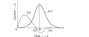
図3はレーザダイオードLD1に流れる電流ILD1及び並列キャパシタC2に流れる電流IC2の波形の例を示す図である。ここで、図1に示したループLP2によって並列キャパシタC2に充電される電流の方向が「正」であり、ループLP3によって並列キャパシタC2から電流が放電される方向が「負」である。FIG. 3 is a diagram showing an example of the waveforms of the current I LD1 flowing through the laser diode LD1 and the current I C2 flowing through the parallel capacitor C2. Here, the direction of the current charged in the parallel capacitor C2 by the loop LP2 shown in FIG. 1 is "positive", and the direction in which the current is discharged from the parallel capacitor C2 by the loop LP3 is "negative".
図3において、時点tz1は電流IC2が正から負に振れ込む時点、tpはレーザダイオードLD1に流れる電流が最大となる時点、tz2は電流IC2が負から正に振れ込む時点である。この例のように、並列キャパシタC2の電流が負である期間に、レーザダイオードLD1に流れる電流が最大となる時点tpがあることが好ましい。つまり、
tz1<tp<tz2の条件を満たすことが好ましい。tz1、tz2、tpの大小関係は並列キャパシタC2の値によって変化するが、上記条件を満たすことにより、並列キャパシタC2の放電電流がレーザダイオードLD1の駆動電流を増強するからである。このことは以降に示す第2の実施形態以降の実施形態についても共通である。In FIG. 3, time tz1 is the time when the current I C2 swings from positive to negative, tp is the time when the current flowing through the laser diode LD1 becomes maximum, and tz2 is the time when the current I C2 swings from negative to positive. As in this example, it is preferable that there is a time point tp at which the current flowing through the laser diode LD1 reaches a maximum during a period when the current in the parallel capacitor C2 is negative. In other words,
It is preferable that the condition tz1<tp<tz2 is satisfied. Although the magnitude relationship of tz1, tz2, and tp changes depending on the value of the parallel capacitor C2, by satisfying the above condition, the discharge current of the parallel capacitor C2 increases the drive current of the laser diode LD1. This is also common to the second embodiment and subsequent embodiments described below.
図4(A)、図4(B)、図4(C)は第1の実施形態に係る別のレーザダイオード駆動回路の回路図である。 4(A), FIG. 4(B), and FIG. 4(C) are circuit diagrams of another laser diode drive circuit according to the first embodiment.
図4(A)に示すレーザダイオード駆動回路101Aは、図1に示したレーザダイオードLD1と第1インダクタL1との位置関係を交換した例である。このレーザダイオード駆動回路101Aと図1に示したレーザダイオード駆動回路101とは回路上は等価である。
A laser
図4(B)に示すレーザダイオード駆動回路101Bは、図1に示した駆動キャパシタC1の位置を変更した例である。駆動キャパシタC1を含むループLP1,LP2はレーザダイオード駆動回路101と等価であるので、このレーザダイオード駆動回路101Bと図1に示したレーザダイオード駆動回路101とは回路上は等価である。
A laser
図4(C)に示すレーザダイオード駆動回路101Cは、図1に示した抵抗素子R1の位置を変更した例である。レーザダイオード駆動回路101Cの駆動キャパシタC1の充電電流経路はレーザダイオード駆動回路101の駆動キャパシタC1の充電電流経路と等価であるので、このレーザダイオード駆動回路101Cと図1に示したレーザダイオード駆動回路101とは回路上は等価である。
A laser
《第2の実施形態》
第2の実施形態では、駆動キャパシタC1の充電電圧を昇圧する回路を含むレーザダイオード駆動回路を例示する。《Second embodiment》
In the second embodiment, a laser diode drive circuit including a circuit that boosts the charging voltage of the drive capacitor C1 is illustrated.
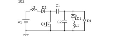
図5は第2の実施形態に係るレーザダイオード駆動回路102の回路図である。このレーザダイオード駆動回路102は、レーザダイオードLD1、駆動キャパシタC1、スイッチ素子Q1、第1インダクタL1、並列キャパシタC2及び第1ダイオードD1を備える。直流電源V1とスイッチ素子Q1との間には、第2インダクタL2及び第2ダイオードD2の直列回路が挿入されている。この第2インダクタL2及び第2ダイオードD2の直列回路を備える構成が第1の実施形態で示したレーザダイオード駆動回路101と異なる。
FIG. 5 is a circuit diagram of the laser
第2の実施形態に係るレーザダイオード駆動回路102においては、スイッチ素子Q1のターンオンにより、直流電源V1→第2インダクタL2→第2ダイオードD2→スイッチ素子Q1の経路で電流が流れ、第2インダクタL2に励磁エネルギーが蓄積される。その後、スイッチ素子Q1のターンオフ時に、直流電源V1→第2ダイオードD2→駆動キャパシタC1や第1ダイオードD1の経路で、駆動キャパシタC1の充電電流が流れる。このとき、昇圧チョッパー回路と同じ作用によって、昇圧された電圧が駆動キャパシタC1に充電される。
In the laser
本実施形態によれば、直流電源V1の電圧より高い電圧でレーザダイオードLD1を駆動することができる。つまり、特別な昇圧回路を別途設けることなく、少ない部品点数で、レーザダイオードLD1を高圧駆動できる。 According to this embodiment, the laser diode LD1 can be driven with a voltage higher than the voltage of the DC power supply V1. In other words, the laser diode LD1 can be driven at high voltage with a small number of components without separately providing a special booster circuit.
《第3の実施形態》
第3の実施形態では、第1、第2の実施形態における第2ループLP2を形成する回路の構成が異なるレーザダイオード駆動回路について例示する。《Third embodiment》
In the third embodiment, a laser diode drive circuit having a different configuration of the circuit forming the second loop LP2 in the first and second embodiments will be exemplified.
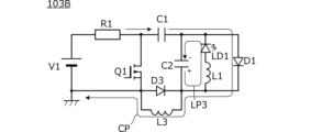
図6は第3の実施形態に係るレーザダイオード駆動回路103Aの回路図である。このレーザダイオード駆動回路103Aは、レーザダイオードLD1、駆動キャパシタC1、スイッチ素子Q1、第1インダクタL1、並列キャパシタC2、第1ダイオードD1及び抵抗素子R1を備える。
FIG. 6 is a circuit diagram of a laser
このレーザダイオード駆動回路103Aでは、第1の実施形態で示したレーザダイオード駆動回路101と異なり、スイッチ素子Q1と並列キャパシタC2との間に、抵抗素子R2と第3ダイオードD3との並列回路が挿入されている。
In this laser
スイッチ素子Q1、駆動キャパシタC1、並列キャパシタC2を含む第2ループLP2には寄生インダクタンスが存在する。この寄生インダクタンスの作用により、駆動キャパシタC1の電圧より並列キャパシタC2の電圧が高くなるときがある。このとき、第3ダイオードD3は、並列キャパシタC2の放電電流がスイッチ素子Q1側へ流れることを阻止する。これにより、図6中に第3ループLP3で示すように、より多くの電流がレーザダイオードLD1に流れることとなり、より大きな瞬時ピーク電流を得られる。抵抗素子R2は、駆動キャパシタC1の充電電流経路CPを形成する。この抵抗素子R2は、第3ダイオードD3の上記作用を確保するため、レーザダイオードLD1のインピーダンスに比べて十分に高いことが必要である。 Parasitic inductance exists in the second loop LP2 including the switch element Q1, the drive capacitor C1, and the parallel capacitor C2. Due to the effect of this parasitic inductance, the voltage of the parallel capacitor C2 may sometimes become higher than the voltage of the drive capacitor C1. At this time, the third diode D3 prevents the discharge current of the parallel capacitor C2 from flowing toward the switching element Q1. As a result, as shown by the third loop LP3 in FIG. 6, more current flows through the laser diode LD1, and a larger instantaneous peak current can be obtained. Resistance element R2 forms a charging current path CP of drive capacitor C1. This resistance element R2 needs to have a sufficiently higher impedance than the laser diode LD1 in order to ensure the above-mentioned effect of the third diode D3.
図7は第3の実施形態に係るもう一つのレーザダイオード駆動回路103Bの回路図である。このレーザダイオード駆動回路103Bは、図6に示したレーザダイオード駆動回路103Aの抵抗素子R2を第3インダクタL3に置換した回路図である。このレーザダイオード駆動回路103Bの構成であっても、第3ダイオードD3は、並列キャパシタC2の放電電流がスイッチ素子Q1側へ流れることを阻止する。また、第3インダクタL3は、並列キャパシタC2の放電電流がスイッチ素子Q1側へ流れようとする過渡電流を抑制するので、第3ダイオードD3の上記作用は確保される。
FIG. 7 is a circuit diagram of another laser
《第4の実施形態》
第4の実施形態では、第1、第2、第3の各実施形態で示した回路とはトポロジーが異なるレーザダイオード駆動回路について例示する。《Fourth embodiment》
In the fourth embodiment, a laser diode drive circuit having a different topology from the circuits shown in the first, second, and third embodiments will be exemplified.
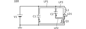
図8は第4の実施形態に係るレーザダイオード駆動回路104の回路図である。このレーザダイオード駆動回路104は、レーザダイオードLD1、駆動キャパシタC1及びスイッチ素子Q1を含んで構成される第1ループLP1と、レーザダイオードLD1に直列接続された第1インダクタL1と、レーザダイオードLD1と第1インダクタL1との直列回路に並列接続された並列キャパシタC2とを備え、駆動キャパシタC1の両端を直流電源の入力部とした回路である。
FIG. 8 is a circuit diagram of a laser
本レーザダイオード駆動回路104は次のように動作する。
This laser
待機時において、スイッチ素子Q1はオフ状態を保つ。この待機時には、駆動キャパシタC1に直流電源V1の電圧が充電されている。 During standby, switch element Q1 remains off. During this standby time, the drive capacitor C1 is charged with the voltage of the DC power supply V1.
レーザダイオードLD1の駆動時は、スイッチ素子Q1がターンオンして、駆動キャパシタC1の電荷が第1ループLP1の経路で放電されることでレーザダイオードLD1が駆動される。また、並列キャパシタC2が第2ループLP2の経路で充電される。 When driving the laser diode LD1, the switching element Q1 is turned on, and the charge in the driving capacitor C1 is discharged through the path of the first loop LP1, thereby driving the laser diode LD1. Further, the parallel capacitor C2 is charged through the path of the second loop LP2.
その後、第3ループLP3の経路で、並列キャパシタC2の放電電流がレーザダイオードLD1を介して流れる。 Thereafter, in the path of the third loop LP3, the discharge current of the parallel capacitor C2 flows through the laser diode LD1.
《第5の実施形態》
第5の実施形態では、第4の実施形態で示したトポロジーのレーザダイオード駆動回路に、並列キャパシタC2の放電電流を規制する素子を設けたレーザダイオード駆動回路について例示する。《Fifth embodiment》
The fifth embodiment will exemplify a laser diode drive circuit in which the laser diode drive circuit having the topology shown in the fourth embodiment is provided with an element that regulates the discharge current of the parallel capacitor C2.
図9は第5の実施形態に係るレーザダイオード駆動回路105の回路図である。このレーザダイオード駆動回路105は、図8に示したレーザダイオード駆動回路104における駆動キャパシタC1と並列キャパシタC2との間に第4ダイオードD4を備えたものである。
FIG. 9 is a circuit diagram of a laser
スイッチ素子Q1、駆動キャパシタC1、並列キャパシタC2を含む第2ループLP2には寄生インダクタンスが存在する。この寄生インダクタンスの作用により、駆動キャパシタC1の電圧より並列キャパシタC2の電圧が高くなるときがある。このとき、第4ダイオードD4は、並列キャパシタC2の放電電流が駆動キャパシタC1側へ流れることを阻止する。そのことにより、並列キャパシタC2の放電電流の全てがレーザダイオードLD1に流れることとなり、より大きな瞬時ピーク電流がレーザダイオードLD1に流れる。 Parasitic inductance exists in the second loop LP2 including the switch element Q1, the drive capacitor C1, and the parallel capacitor C2. Due to the effect of this parasitic inductance, the voltage of the parallel capacitor C2 may become higher than the voltage of the drive capacitor C1. At this time, the fourth diode D4 prevents the discharge current of the parallel capacitor C2 from flowing toward the drive capacitor C1. As a result, all of the discharge current of the parallel capacitor C2 flows to the laser diode LD1, and a larger instantaneous peak current flows to the laser diode LD1.
《第6の実施形態》
第6の実施形態では、第1、第2、第3の各実施形態におけるレーザダイオード駆動回路の駆動キャパシタC1の構成が異なるレーザダイオード駆動回路について例示する。《Sixth embodiment》
In the sixth embodiment, a laser diode drive circuit in which the structure of the drive capacitor C1 of the laser diode drive circuit in each of the first, second, and third embodiments is different will be illustrated.
図10(A)、図10(B)は、第6の実施形態に係るレーザダイオード駆動回路106Aの回路図である。図10(A)は図1に示したレーザダイオード駆動回路101における駆動キャパシタC1を直流電源V1に置換し、第1ダイオードD1を削除した回路である。図10(B)は図10(A)に示す回路を一般的な形で表した図である。
FIGS. 10A and 10B are circuit diagrams of a laser
レーザダイオード駆動回路106Aの動作は次のとおりである。
The operation of the laser
レーザダイオードLD1の駆動時は、スイッチ素子Q1がターンオンして、直流電源V1→スイッチ素子Q1→第1インダクタL1→レーザダイオードLD1の経路(第1ループLP1)でレーザダイオードLD1の駆動電流が流れる。また、直流電源V1→スイッチ素子Q1→並列キャパシタC2の経路(第2ループLP2)で、並列キャパシタC2に充電電流が流れる。その後、並列キャパシタC2の放電電流が第3ループLP3を介して流れる。 When driving the laser diode LD1, the switch element Q1 is turned on, and the drive current for the laser diode LD1 flows through the path (first loop LP1) of DC power supply V1 → switch element Q1 → first inductor L1 → laser diode LD1. Further, a charging current flows through the parallel capacitor C2 through a path (second loop LP2) of DC power supply V1→switch element Q1→parallel capacitor C2. Thereafter, the discharge current of the parallel capacitor C2 flows through the third loop LP3.
その後、スイッチ素子Q1がターンオフすることにより、レーザダイオードLD1の電流が0となる。 Thereafter, the switch element Q1 is turned off, so that the current of the laser diode LD1 becomes zero.
図11は第6の実施形態に係る別のレーザダイオード駆動回路106Bの回路図である。上記レーザダイオード駆動回路106Aでは直流電源を負電源としたが、このレーザダイオード駆動回路106Bでは直流電源を正電源とした例である。回路動作は上記レーザダイオード駆動回路106Aと同様である。
FIG. 11 is a circuit diagram of another laser
《第7の実施形態》
第7の実施形態では、第4の実施形態におけるレーザダイオード駆動回路の駆動キャパシタC1の構成が異なるレーザダイオード駆動回路について例示する。《Seventh embodiment》
In the seventh embodiment, a laser diode drive circuit in which the configuration of the drive capacitor C1 of the laser diode drive circuit in the fourth embodiment is different will be exemplified.
図12は第7の実施形態に係るレーザダイオード駆動回路107の回路図である。このレーザダイオード駆動回路107は図8に示したレーザダイオード駆動回路104における駆動キャパシタC1を直流電源V1に置換した回路である。
FIG. 12 is a circuit diagram of a laser
レーザダイオード駆動回路107の動作は次のとおりである。
The operation of the laser
レーザダイオードLD1の駆動時は、スイッチ素子Q1がターンオンして、直流電源V1→第1インダクタL1→レーザダイオードLD1→スイッチ素子Q1の経路(第1ループLP1)でレーザダイオードLD1の駆動電流が流れる。また、直流電源V1→並列キャパシタC2→スイッチ素子Q1の経路(第2ループLP2)で、並列キャパシタC2に充電電流が流れる。その後、並列キャパシタC2の放電電流が第3ループLP3を介して流れる。 When the laser diode LD1 is driven, the switch element Q1 is turned on, and the driving current of the laser diode LD1 flows through the path (first loop LP1) of DC power supply V1 → first inductor L1 → laser diode LD1 → switch element Q1. Further, a charging current flows through the parallel capacitor C2 through a path (second loop LP2) of DC power supply V1→parallel capacitor C2→switch element Q1. Thereafter, the discharge current of the parallel capacitor C2 flows through the third loop LP3.
その後、スイッチ素子Q1がターンオフすることにより、レーザダイオードLD1の電流が0となる。 Thereafter, the switch element Q1 is turned off, so that the current of the laser diode LD1 becomes zero.
《第8の実施形態》
第8の実施形態では、第5の実施形態におけるレーザダイオード駆動回路の駆動キャパシタC1の構成が異なるレーザダイオード駆動回路について例示する。《Eighth embodiment》
In the eighth embodiment, a laser diode drive circuit in which the configuration of the drive capacitor C1 of the laser diode drive circuit in the fifth embodiment is different will be exemplified.
図13は第8の実施形態に係るレーザダイオード駆動回路108の回路図である。このレーザダイオード駆動回路108は図9に示したレーザダイオード駆動回路105における駆動キャパシタC1を直流電源V1に置換した回路である。
FIG. 13 is a circuit diagram of a laser
レーザダイオード駆動回路108の動作は次のとおりである。
The operation of the laser
レーザダイオードLD1の駆動時は、スイッチ素子Q1がターンオンして、直流電源V1→第4ダイオードD4→第1インダクタL1→レーザダイオードLD1→スイッチ素子Q1の経路でレーザダイオードLD1の駆動電流が流れる。また、直流電源V1→第4ダイオードD4→並列キャパシタC2→スイッチ素子Q1の経路で、並列キャパシタC2に充電電流が流れる。その後、並列キャパシタC2の放電電流がレーザダイオードLD1に流れる。 When the laser diode LD1 is driven, the switch element Q1 is turned on, and the drive current of the laser diode LD1 flows through the path of DC power supply V1 → fourth diode D4 → first inductor L1 → laser diode LD1 → switch element Q1. Further, a charging current flows through the parallel capacitor C2 through a path of DC power supply V1→fourth diode D4→parallel capacitor C2→switch element Q1. Thereafter, the discharge current of the parallel capacitor C2 flows to the laser diode LD1.
その後、スイッチ素子Q1がターンオフすることにより、レーザダイオードLD1の電流が0となる。 Thereafter, the switch element Q1 is turned off, so that the current of the laser diode LD1 becomes zero.
スイッチ素子Q1、駆動キャパシタC1、並列キャパシタC2を含む第2ループLP2には寄生インダクタンスが存在する。この寄生インダクタンスの作用により、駆動キャパシタC1の電圧より並列キャパシタC2の電圧が高くなるときがある。このとき、第4ダイオードD4は、並列キャパシタC2の放電電流が直流電源V1側へ流れることを阻止する。 Parasitic inductance exists in the second loop LP2 including the switch element Q1, the drive capacitor C1, and the parallel capacitor C2. Due to the effect of this parasitic inductance, the voltage of the parallel capacitor C2 may become higher than the voltage of the drive capacitor C1. At this time, the fourth diode D4 prevents the discharge current of the parallel capacitor C2 from flowing toward the DC power supply V1.
最後に、本発明は上述した実施形態に限られるものではない。当業者によって適宜変形及び変更が可能である。本発明の範囲は、上述の実施形態ではなく、特許請求の範囲によって示される。さらに、本発明の範囲には、特許請求の範囲内と均等の範囲内での実施形態からの変形及び変更が含まれる。 Finally, the invention is not limited to the embodiments described above. Appropriate modifications and changes can be made by those skilled in the art. The scope of the invention is indicated by the claims rather than the embodiments described above. Furthermore, the scope of the present invention includes modifications and changes from the embodiments within the scope of the claims and equivalents.
例えば、各実施形態で示した第1インダクタL1は、レーザダイオードLD1に関する配線部が有する寄生インダクタンスで構成されていてもよい。また、インダクタと寄生インダクタンスとの合成インダクタンスを第1インダクタL1として使用してもよい。 For example, the first inductor L1 shown in each embodiment may be configured by a parasitic inductance included in a wiring section related to the laser diode LD1. Further, a composite inductance of an inductor and a parasitic inductance may be used as the first inductor L1.
また、各実施形態で示した並列キャパシタC2は、レーザダイオードLD1に関する配線部が有する寄生キャパシタンスで構成されていてもよい。また、キャパシタと寄生キャパシタンスとの合成キャパシタンスを並列キャパシタC2として使用してもよい。 Moreover, the parallel capacitor C2 shown in each embodiment may be configured by a parasitic capacitance included in the wiring section related to the laser diode LD1. Further, a combined capacitance of a capacitor and a parasitic capacitance may be used as the parallel capacitor C2.
C1…駆動キャパシタ
C2…並列キャパシタ
CP…充電電流経路
D1…第1ダイオード
D2…第2ダイオード
D3…第3ダイオード
D4…第4ダイオード
L1…第1インダクタ
L2…第2インダクタ
L3…第3インダクタ
LD1…レーザダイオード
LP1…第1ループ
LP2…第2ループ
LP3…第3ループ
Q1…スイッチ素子
R1,R2…抵抗素子
V1…直流電源
101,101A,101B,101C,102,103A,103B,104,105,106A,106B,107,108…レーザダイオード駆動回路C1... Drive capacitor C2... Parallel capacitor CP... Charging current path D1... First diode D2... Second diode D3... Third diode D4... Fourth diode L1... First inductor L2... Second inductor L3... Third inductor LD1... Laser diode LP1...first loop LP2...second loop LP3...third loop Q1...switch element R1, R2...resistance element V1...
Claims (7)
前記スイッチ素子の第1端と前記並列キャパシタとの間で前記ループに直列に、抵抗素子と逆流防止用の第3ダイオードとの並列回路、又はインダクタと逆流防止用の第3ダイオードとの並列回路、が挿入された、
レーザダイオード駆動回路。 a loop including a laser diode, a drive capacitor for accumulating drive charge, and a switch element; a first inductor connected in series to the laser diode; and a series circuit including the laser diode and the first inductor. a parallel capacitor connected in parallel; and a first diode connected in parallel to the series circuit with a polarity opposite to that of the laser diode, and a first end of the switch element is connected to a first end of a DC power supply. a second end of the switch element is connected to a second end of the DC power source, the second end of the DC power source has a higher potential than the first end of the DC power source, and the cathode of the laser diode is connected to the second end of the DC power source; connected to the second end of the DC power supply ,
A parallel circuit of a resistive element and a third diode for backflow prevention, or a parallel circuit of an inductor and a third diode for backflow prevention, in series with the loop between the first end of the switch element and the parallel capacitor. , was inserted ,
Laser diode drive circuit.
前記並列キャパシタのキャパシタンスをC2、前記第1インダクタのインダクタンスをL1、前記レーザダイオードの抵抗成分をRLD1でそれぞれ表すとき、
R2 LD1 < 4L1/C2
の関係にある、
レーザダイオード駆動回路。 a loop including a laser diode, a drive capacitor for accumulating drive charge, and a switch element; a first inductor connected in series to the laser diode; and a series circuit including the laser diode and the first inductor. a parallel capacitor connected in parallel; and a first diode connected in parallel to the series circuit with a polarity opposite to that of the laser diode, and a first end of the switch element is connected to a first end of a DC power supply. a second end of the switch element is connected to a second end of the DC power source, the second end of the DC power source has a higher potential than the first end of the DC power source, and the cathode of the laser diode is connected to the second end of the DC power source; connected to the second end of the DC power supply,
When the capacitance of the parallel capacitor is represented by C2, the inductance of the first inductor is represented by L1, and the resistance component of the laser diode is represented by RLD1 ,
R 2 LD1 < 4L1/C2
In the relationship of
Laser diode drive circuit.
請求項1又は2に記載のレーザダイオード駆動回路。 A series circuit of a second inductor and a second diode is inserted between a second end of the DC power supply and a second end of the switch element.
A laser diode drive circuit according to claim 1 or 2.
請求項1から3のいずれかに記載のレーザダイオード駆動回路。 When the switch element is turned on, a current flowing through the circuit formed by the parallel capacitor, the first inductor, and the laser diode is a damped oscillating current, and the point at which the damped oscillating current reaches its peak is when the switch element is turned on. coincides with the point in time when the current flowing through the loop including the laser diode and the switching element reaches its peak ,
A laser diode drive circuit according to any one of claims 1 to 3 .
Tz1<Tp<Tz2
の関係となる値である、
請求項1から4のいずれかに記載のレーザダイオード駆動回路。 The time point at which the current flowing through the parallel capacitor changes from the forward direction to the reverse direction by turning on the switch element is Tz1, the time point at which the current flowing through the parallel capacitor changes from the reverse direction to the forward direction by turning on the switch element is Tz2, and the switch When the point at which the current flowing through the laser diode reaches its peak when the device is turned on is expressed as Tp, the capacitance of the parallel capacitor is:
Tz1<Tp<Tz2
is the value related to
A laser diode drive circuit according to any one of claims 1 to 4 .
請求項1から5のいずれかに記載のレーザダイオード駆動回路。 The first inductor is constituted by a parasitic inductance of a wiring section related to the laser diode.
A laser diode drive circuit according to any one of claims 1 to 5 .
請求項1から6のいずれかに記載のレーザダイオード駆動回路。 The parallel capacitor is constituted by a parasitic capacitance of a wiring section related to the laser diode.
A laser diode drive circuit according to any one of claims 1 to 6 .
Priority Applications (1)
| Application Number | Priority Date | Filing Date | Title |
|---|---|---|---|
| JP2023200427A JP2024022614A (en) | 2020-04-15 | 2023-11-28 | Laser diode drive circuit |
Applications Claiming Priority (3)
| Application Number | Priority Date | Filing Date | Title |
|---|---|---|---|
| JP2020072989 | 2020-04-15 | ||
| JP2020072989 | 2020-04-15 | ||
| PCT/JP2020/045892 WO2021210217A1 (en) | 2020-04-15 | 2020-12-09 | Laser diode driving circuit |
Related Child Applications (1)
| Application Number | Title | Priority Date | Filing Date |
|---|---|---|---|
| JP2023200427A Division JP2024022614A (en) | 2020-04-15 | 2023-11-28 | Laser diode drive circuit |
Publications (3)
| Publication Number | Publication Date |
|---|---|
| JPWO2021210217A1 JPWO2021210217A1 (en) | 2021-10-21 |
| JPWO2021210217A5 JPWO2021210217A5 (en) | 2022-10-03 |
| JP7396470B2 true JP7396470B2 (en) | 2023-12-12 |
Family
ID=78083688
Family Applications (2)
| Application Number | Title | Priority Date | Filing Date |
|---|---|---|---|
| JP2022515203A Active JP7396470B2 (en) | 2020-04-15 | 2020-12-09 | Laser diode drive circuit |
| JP2023200427A Pending JP2024022614A (en) | 2020-04-15 | 2023-11-28 | Laser diode drive circuit |
Family Applications After (1)
| Application Number | Title | Priority Date | Filing Date |
|---|---|---|---|
| JP2023200427A Pending JP2024022614A (en) | 2020-04-15 | 2023-11-28 | Laser diode drive circuit |
Country Status (5)
| Country | Link |
|---|---|
| US (1) | US20220376472A1 (en) |
| JP (2) | JP7396470B2 (en) |
| CN (1) | CN115004490A (en) |
| DE (1) | DE112020006729T5 (en) |
| WO (1) | WO2021210217A1 (en) |
Families Citing this family (1)
| Publication number | Priority date | Publication date | Assignee | Title |
|---|---|---|---|---|
| JP7466773B1 (en) | 2022-12-23 | 2024-04-12 | 三菱電機株式会社 | Optical Modules |
Citations (16)
| Publication number | Priority date | Publication date | Assignee | Title |
|---|---|---|---|---|
| US20070280314A1 (en) | 2006-06-01 | 2007-12-06 | Yong-Chan Keh | Integrated circuit for driving a light source |
| JP2009544022A (en) | 2006-07-17 | 2009-12-10 | ライカ ジオシステムズ アクチェンゲゼルシャフト | Electro-optical distance meter |
| JP2012033541A (en) | 2010-07-28 | 2012-02-16 | Miyachi Technos Corp | Mopa system fiber laser processing device and laser diode power supply device for seed |
| JP2012114338A (en) | 2010-11-26 | 2012-06-14 | Sharp Corp | Laser light-emitting device and vehicle lamp using the same |
| JP2015179436A (en) | 2014-03-19 | 2015-10-08 | 古河電気工業株式会社 | Drive circuit of light-emitting element, light source device, and driving method of light-emitting element |
| CN204885822U (en) | 2015-09-14 | 2015-12-16 | 深圳市迅捷光通科技有限公司 | Semiconductor laser drive circuit reaches semiconductor laser including this circuit |
| JP2016152336A (en) | 2015-02-18 | 2016-08-22 | 株式会社豊田中央研究所 | Laser diode driving circuit and laser radar device |
| JP2017028235A (en) | 2015-07-27 | 2017-02-02 | 株式会社トリマティス | Short pulse laser light-emitting drive circuit |
| JP2017139704A (en) | 2016-02-05 | 2017-08-10 | パイオニア株式会社 | Driving device for light emitting unit |
| JP2018059839A (en) | 2016-10-06 | 2018-04-12 | 株式会社デンソー | Distance measurement device |
| WO2018150459A1 (en) | 2017-02-14 | 2018-08-23 | 三菱電機株式会社 | Laser diode driving power source and laser machining device |
| US20180261975A1 (en) | 2017-03-07 | 2018-09-13 | Sensl Technologies Ltd. | Laser driver |
| WO2019207938A1 (en) | 2018-04-26 | 2019-10-31 | 株式会社村田製作所 | Light emitting device and capacitor |
| CN110535028A (en) | 2019-08-16 | 2019-12-03 | 上海禾赛光电科技有限公司 | For the safe charging circuit of light emitting module, guard method and laser radar emission system |
| JP2020506399A (en) | 2016-12-30 | 2020-02-27 | パノセンス インコーポレイテッド | Rider system |
| JP2020506400A (en) | 2016-12-30 | 2020-02-27 | パノセンス インコーポレイテッド | Laser power calibration and correction |
-
2020
- 2020-12-09 CN CN202080094831.3A patent/CN115004490A/en active Pending
- 2020-12-09 JP JP2022515203A patent/JP7396470B2/en active Active
- 2020-12-09 WO PCT/JP2020/045892 patent/WO2021210217A1/en active Application Filing
- 2020-12-09 DE DE112020006729.7T patent/DE112020006729T5/en active Pending
-
2022
- 2022-07-28 US US17/875,962 patent/US20220376472A1/en active Pending
-
2023
- 2023-11-28 JP JP2023200427A patent/JP2024022614A/en active Pending
Patent Citations (16)
| Publication number | Priority date | Publication date | Assignee | Title |
|---|---|---|---|---|
| US20070280314A1 (en) | 2006-06-01 | 2007-12-06 | Yong-Chan Keh | Integrated circuit for driving a light source |
| JP2009544022A (en) | 2006-07-17 | 2009-12-10 | ライカ ジオシステムズ アクチェンゲゼルシャフト | Electro-optical distance meter |
| JP2012033541A (en) | 2010-07-28 | 2012-02-16 | Miyachi Technos Corp | Mopa system fiber laser processing device and laser diode power supply device for seed |
| JP2012114338A (en) | 2010-11-26 | 2012-06-14 | Sharp Corp | Laser light-emitting device and vehicle lamp using the same |
| JP2015179436A (en) | 2014-03-19 | 2015-10-08 | 古河電気工業株式会社 | Drive circuit of light-emitting element, light source device, and driving method of light-emitting element |
| JP2016152336A (en) | 2015-02-18 | 2016-08-22 | 株式会社豊田中央研究所 | Laser diode driving circuit and laser radar device |
| JP2017028235A (en) | 2015-07-27 | 2017-02-02 | 株式会社トリマティス | Short pulse laser light-emitting drive circuit |
| CN204885822U (en) | 2015-09-14 | 2015-12-16 | 深圳市迅捷光通科技有限公司 | Semiconductor laser drive circuit reaches semiconductor laser including this circuit |
| JP2017139704A (en) | 2016-02-05 | 2017-08-10 | パイオニア株式会社 | Driving device for light emitting unit |
| JP2018059839A (en) | 2016-10-06 | 2018-04-12 | 株式会社デンソー | Distance measurement device |
| JP2020506399A (en) | 2016-12-30 | 2020-02-27 | パノセンス インコーポレイテッド | Rider system |
| JP2020506400A (en) | 2016-12-30 | 2020-02-27 | パノセンス インコーポレイテッド | Laser power calibration and correction |
| WO2018150459A1 (en) | 2017-02-14 | 2018-08-23 | 三菱電機株式会社 | Laser diode driving power source and laser machining device |
| US20180261975A1 (en) | 2017-03-07 | 2018-09-13 | Sensl Technologies Ltd. | Laser driver |
| WO2019207938A1 (en) | 2018-04-26 | 2019-10-31 | 株式会社村田製作所 | Light emitting device and capacitor |
| CN110535028A (en) | 2019-08-16 | 2019-12-03 | 上海禾赛光电科技有限公司 | For the safe charging circuit of light emitting module, guard method and laser radar emission system |
Also Published As
| Publication number | Publication date |
|---|---|
| JP2024022614A (en) | 2024-02-16 |
| CN115004490A (en) | 2022-09-02 |
| US20220376472A1 (en) | 2022-11-24 |
| DE112020006729T5 (en) | 2022-12-01 |
| JPWO2021210217A1 (en) | 2021-10-21 |
| WO2021210217A1 (en) | 2021-10-21 |
Similar Documents
| Publication | Publication Date | Title |
|---|---|---|
| JP5169135B2 (en) | Switching power supply | |
| JP2024022614A (en) | Laser diode drive circuit | |
| JP2012090387A (en) | Dc-dc converter | |
| KR20100034712A (en) | Light-emitting element drive controlling circuit | |
| JP2003235256A (en) | Switching power unit | |
| KR20010109143A (en) | Drive circuit of capacitive load and integrated circuit for driving capacitive load | |
| JP2007043852A (en) | Method, program, and circuit for controlling dc-dc converter | |
| JP5216819B2 (en) | Power supply | |
| US10499469B2 (en) | Strobe apparatus having light-emitting semiconductor module driven by two-stepped drive current | |
| JP4519613B2 (en) | LED lighting device | |
| JP2012079680A (en) | Discharge lamp lighting circuit | |
| JP4687889B2 (en) | Discharge lamp lighting device | |
| JP2010198860A (en) | Discharge lamp-lighting circuit | |
| JP2015150910A (en) | Device and method for driving lamps for vehicle | |
| JP2006080024A (en) | Discharge lamp lighting device | |
| US5442260A (en) | Light-emitting element drive circuit | |
| KR940003431A (en) | Electronic ballast circuit for discharge lamp | |
| JP2004147436A (en) | Dc-dc converter | |
| JP2017123261A (en) | Power supply device for led and led lighting device | |
| JP3469455B2 (en) | Switching power supply | |
| JP2008067531A (en) | Switching control circuit | |
| JP3761548B2 (en) | DC-DC converter and piezoelectric vibrator drive circuit | |
| JP2005011798A (en) | High voltage pulse generating device and discharge lamp lighting device | |
| JP2006147360A (en) | Light-emitting diode lighting device | |
| JP5029199B2 (en) | Discharge lamp lighting device |
Legal Events
| Date | Code | Title | Description |
|---|---|---|---|
| A521 | Request for written amendment filed |
Free format text: JAPANESE INTERMEDIATE CODE: A523 Effective date: 20220728 |
|
| A621 | Written request for application examination |
Free format text: JAPANESE INTERMEDIATE CODE: A621 Effective date: 20220728 |
|
| A977 | Report on retrieval |
Free format text: JAPANESE INTERMEDIATE CODE: A971007 Effective date: 20230724 |
|
| A131 | Notification of reasons for refusal |
Free format text: JAPANESE INTERMEDIATE CODE: A131 Effective date: 20230815 |
|
| A521 | Request for written amendment filed |
Free format text: JAPANESE INTERMEDIATE CODE: A523 Effective date: 20231002 |
|
| TRDD | Decision of grant or rejection written | ||
| A01 | Written decision to grant a patent or to grant a registration (utility model) |
Free format text: JAPANESE INTERMEDIATE CODE: A01 Effective date: 20231031 |
|
| A61 | First payment of annual fees (during grant procedure) |
Free format text: JAPANESE INTERMEDIATE CODE: A61 Effective date: 20231113 |
|
| R150 | Certificate of patent or registration of utility model |
Ref document number: 7396470 Country of ref document: JP Free format text: JAPANESE INTERMEDIATE CODE: R150 |