JP7369047B2 - Optical modules and optical transmission equipment - Google Patents
Optical modules and optical transmission equipment Download PDFInfo
- Publication number
- JP7369047B2 JP7369047B2 JP2020013555A JP2020013555A JP7369047B2 JP 7369047 B2 JP7369047 B2 JP 7369047B2 JP 2020013555 A JP2020013555 A JP 2020013555A JP 2020013555 A JP2020013555 A JP 2020013555A JP 7369047 B2 JP7369047 B2 JP 7369047B2
- Authority
- JP
- Japan
- Prior art keywords
- optical
- transmission line
- optical module
- differential
- circuit
- Prior art date
- Legal status (The legal status is an assumption and is not a legal conclusion. Google has not performed a legal analysis and makes no representation as to the accuracy of the status listed.)
- Active
Links
- 230000005540 biological transmission Effects 0.000 title claims description 215
- 230000003287 optical effect Effects 0.000 title claims description 185
- 239000000758 substrate Substances 0.000 claims description 26
- 239000003990 capacitor Substances 0.000 claims description 23
- 230000000903 blocking effect Effects 0.000 claims description 5
- 239000011888 foil Substances 0.000 claims description 2
- 239000004065 semiconductor Substances 0.000 description 60
- 239000004020 conductor Substances 0.000 description 40
- 238000010521 absorption reaction Methods 0.000 description 34
- 239000010410 layer Substances 0.000 description 28
- 238000010586 diagram Methods 0.000 description 13
- 230000000694 effects Effects 0.000 description 6
- 239000002184 metal Substances 0.000 description 5
- 229910052751 metal Inorganic materials 0.000 description 5
- 239000011521 glass Substances 0.000 description 4
- 239000000463 material Substances 0.000 description 4
- 238000006243 chemical reaction Methods 0.000 description 3
- 230000005672 electromagnetic field Effects 0.000 description 3
- 238000000034 method Methods 0.000 description 3
- RYGMFSIKBFXOCR-UHFFFAOYSA-N Copper Chemical compound [Cu] RYGMFSIKBFXOCR-UHFFFAOYSA-N 0.000 description 2
- 230000008901 benefit Effects 0.000 description 2
- 230000008859 change Effects 0.000 description 2
- 229910052802 copper Inorganic materials 0.000 description 2
- 239000010949 copper Substances 0.000 description 2
- 239000003822 epoxy resin Substances 0.000 description 2
- 238000004519 manufacturing process Methods 0.000 description 2
- 239000013307 optical fiber Substances 0.000 description 2
- 229920000647 polyepoxide Polymers 0.000 description 2
- 229920001721 polyimide Polymers 0.000 description 2
- 230000009467 reduction Effects 0.000 description 2
- 239000011324 bead Substances 0.000 description 1
- 230000008033 biological extinction Effects 0.000 description 1
- 238000004891 communication Methods 0.000 description 1
- 238000013461 design Methods 0.000 description 1
- 238000011156 evaluation Methods 0.000 description 1
- 239000004744 fabric Substances 0.000 description 1
- 238000012986 modification Methods 0.000 description 1
- 230000004048 modification Effects 0.000 description 1
- 238000012545 processing Methods 0.000 description 1
- 230000004044 response Effects 0.000 description 1
- 230000008054 signal transmission Effects 0.000 description 1
- 239000002344 surface layer Substances 0.000 description 1
- 229910000859 α-Fe Inorganic materials 0.000 description 1
Images


Classifications
-
- G—PHYSICS
- G02—OPTICS
- G02B—OPTICAL ELEMENTS, SYSTEMS OR APPARATUS
- G02B6/00—Light guides; Structural details of arrangements comprising light guides and other optical elements, e.g. couplings
- G02B6/24—Coupling light guides
- G02B6/42—Coupling light guides with opto-electronic elements
- G02B6/4201—Packages, e.g. shape, construction, internal or external details
- G02B6/4256—Details of housings
- G02B6/4262—Details of housings characterised by the shape of the housing
- G02B6/4263—Details of housings characterised by the shape of the housing of the transisitor outline [TO] can type
-
- H—ELECTRICITY
- H04—ELECTRIC COMMUNICATION TECHNIQUE
- H04B—TRANSMISSION
- H04B10/00—Transmission systems employing electromagnetic waves other than radio-waves, e.g. infrared, visible or ultraviolet light, or employing corpuscular radiation, e.g. quantum communication
- H04B10/40—Transceivers
-
- G—PHYSICS
- G02—OPTICS
- G02B—OPTICAL ELEMENTS, SYSTEMS OR APPARATUS
- G02B6/00—Light guides; Structural details of arrangements comprising light guides and other optical elements, e.g. couplings
- G02B6/24—Coupling light guides
- G02B6/42—Coupling light guides with opto-electronic elements
- G02B6/4201—Packages, e.g. shape, construction, internal or external details
- G02B6/4274—Electrical aspects
- G02B6/428—Electrical aspects containing printed circuit boards [PCB]
- G02B6/4281—Electrical aspects containing printed circuit boards [PCB] the printed circuit boards being flexible
-
- H—ELECTRICITY
- H01—ELECTRIC ELEMENTS
- H01S—DEVICES USING THE PROCESS OF LIGHT AMPLIFICATION BY STIMULATED EMISSION OF RADIATION [LASER] TO AMPLIFY OR GENERATE LIGHT; DEVICES USING STIMULATED EMISSION OF ELECTROMAGNETIC RADIATION IN WAVE RANGES OTHER THAN OPTICAL
- H01S5/00—Semiconductor lasers
- H01S5/02—Structural details or components not essential to laser action
- H01S5/022—Mountings; Housings
- H01S5/02208—Mountings; Housings characterised by the shape of the housings
- H01S5/02212—Can-type, e.g. TO-CAN housings with emission along or parallel to symmetry axis
-
- H—ELECTRICITY
- H01—ELECTRIC ELEMENTS
- H01S—DEVICES USING THE PROCESS OF LIGHT AMPLIFICATION BY STIMULATED EMISSION OF RADIATION [LASER] TO AMPLIFY OR GENERATE LIGHT; DEVICES USING STIMULATED EMISSION OF ELECTROMAGNETIC RADIATION IN WAVE RANGES OTHER THAN OPTICAL
- H01S5/00—Semiconductor lasers
- H01S5/02—Structural details or components not essential to laser action
- H01S5/022—Mountings; Housings
- H01S5/023—Mount members, e.g. sub-mount members
- H01S5/02325—Mechanically integrated components on mount members or optical micro-benches
-
- H—ELECTRICITY
- H01—ELECTRIC ELEMENTS
- H01S—DEVICES USING THE PROCESS OF LIGHT AMPLIFICATION BY STIMULATED EMISSION OF RADIATION [LASER] TO AMPLIFY OR GENERATE LIGHT; DEVICES USING STIMULATED EMISSION OF ELECTROMAGNETIC RADIATION IN WAVE RANGES OTHER THAN OPTICAL
- H01S5/00—Semiconductor lasers
- H01S5/04—Processes or apparatus for excitation, e.g. pumping, e.g. by electron beams
- H01S5/042—Electrical excitation ; Circuits therefor
- H01S5/0427—Electrical excitation ; Circuits therefor for applying modulation to the laser
-
- H—ELECTRICITY
- H04—ELECTRIC COMMUNICATION TECHNIQUE
- H04B—TRANSMISSION
- H04B10/00—Transmission systems employing electromagnetic waves other than radio-waves, e.g. infrared, visible or ultraviolet light, or employing corpuscular radiation, e.g. quantum communication
- H04B10/50—Transmitters
- H04B10/501—Structural aspects
- H04B10/503—Laser transmitters
- H04B10/504—Laser transmitters using direct modulation
Description
本発明は、光モジュール及び光伝送装置に関し、特に、電気信号から光信号に変換する光送信回路に関する。 The present invention relates to an optical module and an optical transmission device, and particularly to an optical transmission circuit that converts an electrical signal into an optical signal.
光通信システムにおいて、電気信号を光信号に変換する光送信回路や、光信号を電気信号に変換する光受信回路を内蔵した光モジュールが用いられている。通常用いられている光モジュールは送信機能と受信機能との両方を備えた光送受信機(光トランシーバモジュール)である。光トランシーバモジュールは近年のブロードバンドネットワークの普及と共に高速化、小型・低コスト化が図られ、高速化に関しては変調レートが25~28ギガビット/秒[Gbit/s]のものが広く用いられるようになってきている。小型・低コスト化に関しては例えばSFP28(Small Form-factor Pluggable 28)のMSA(Multi-Source Agreement)規格のようにケース体積の縮小化・部品数の削減化が進んでいる。 Optical communication systems use optical modules that include optical transmission circuits that convert electrical signals into optical signals and optical receiving circuits that convert optical signals into electrical signals. A commonly used optical module is an optical transceiver (optical transceiver module) that has both a transmitting function and a receiving function. With the spread of broadband networks in recent years, optical transceiver modules have become faster, smaller, and lower in cost.In terms of higher speeds, modules with modulation rates of 25 to 28 Gbit/s are now widely used. It's coming. Regarding miniaturization and cost reduction, progress is being made in reducing the case volume and the number of parts, such as the MSA (Multi-Source Agreement) standard for SFP28 (Small Form-factor Pluggable 28).
光モジュールは1つのケース内に、光サブアセンブリ(Optical Subassembly:OSA)と、リジッド基板からなる回路基板と、それら光サブアセンブリと回路基板とを接続するフレキシブル基板とを収める。光サブアセンブリには、光送信回路に用いられるTOSA(Transmitter Optical Subassembly)と、光受信回路に用いられるROSA(Receiver Optical Subassembly)とがある。 An optical module houses an optical subassembly (OSA), a circuit board made of a rigid board, and a flexible board that connects the optical subassembly and the circuit board in one case. Optical subassemblies include TOSA (Transmitter Optical Subassembly) used for optical transmission circuits and ROSA (Receiver Optical Subassembly) used for optical reception circuits.
TOSAは回路基板から入力された電気信号を光信号に変換して出力する。TOSAには発光素子や光変調器が内蔵される。例えば、長距離、高速の伝送には光源・光変調器として、半導体レーザであるDFB-LD(Distributed Feedback Laser Diode:分布帰還型レーザダイオード)を直接変調するものが多く用いられている。ちなみに、直接変調方式の光変調器では、TOSAの外部の駆動回路から半導体レーザに供給する駆動電流を伝送信号に応じて変調することで、レーザ光出力に変調が加えられる。TOSAのパッケージ形態としては、低コスト化のためTO-CAN型のものが多く採用されている。ちなみに、TO-CANパッケージは、半導体レーザなどの光出力素子を取り付けたステムにキャップを被せた構造を有し、また、ステムを貫通するリードピンを介してパッケージの内部と外部との電気的な接続が行われる。 TOSA converts an electrical signal input from a circuit board into an optical signal and outputs it. TOSA has a built-in light emitting element and optical modulator. For example, for long-distance, high-speed transmission, a light source/light modulator that directly modulates a DFB-LD (Distributed Feedback Laser Diode), which is a semiconductor laser, is often used. Incidentally, in a direct modulation type optical modulator, modulation is applied to the laser light output by modulating the drive current supplied to the semiconductor laser from a drive circuit external to the TOSA according to a transmission signal. As the package form of TOSA, TO-CAN type is often adopted for cost reduction. Incidentally, the TO-CAN package has a structure in which a cap is placed over a stem to which an optical output device such as a semiconductor laser is attached, and electrical connections between the inside and outside of the package are made through lead pins that pass through the stem. will be held.
光送信回路は、TOSAに変調信号として入力される電気信号を生成する駆動回路を有する。駆動回路は集積回路(Integrated Circuit:IC)として構成され、当該駆動ICは回路基板に配置される。 The optical transmission circuit has a drive circuit that generates an electrical signal that is input as a modulation signal to the TOSA. The drive circuit is configured as an integrated circuit (IC), and the drive IC is arranged on a circuit board.
駆動回路から出力される変調信号は光信号の高い伝送速度に対応して基本的に高周波信号であり、駆動回路とTOSAとの間は当該高周波信号を通すよう、マイクロストリップライン、ストリップラインなどの伝送線路で接続される。また、TO-CANパッケージのリードピンの部分も、リードピンとそれが貫通するステムの孔との間には隙間が設けられ、当該隙間には誘電体としてガラスが埋め込まれ、同軸形状の伝送線路に構成されている(下記特許文献2)。
The modulation signal output from the drive circuit is basically a high frequency signal corresponding to the high transmission speed of the optical signal, and a microstrip line, strip line, etc. is used between the drive circuit and TOSA to pass the high frequency signal. Connected by transmission line. In addition, in the lead pin portion of the TO-CAN package, a gap is provided between the lead pin and the hole in the stem through which it passes, and glass is embedded as a dielectric in the gap, forming a coaxial transmission line. (
また、半導体レーザの電流振幅を大きくする、すなわち半導体レーザから出力される光信号の消光比を充分に高くするべく、半導体レーザと駆動ICとを平衡接続とし、さらに駆動ICの差動出力インピーダンスを、電子回路では一般的である100オーム[Ω]の半分である50Ωとする構成が普及している。つまり、当該構成では駆動ICと半導体レーザとの間を一対の伝送線路からなる差動伝送線路で接続し、その差動インピーダンスは50Ωとする。 In addition, in order to increase the current amplitude of the semiconductor laser, that is, to sufficiently increase the extinction ratio of the optical signal output from the semiconductor laser, the semiconductor laser and the drive IC are connected in a balanced manner, and the differential output impedance of the drive IC is also increased. In electronic circuits, a configuration of 50 Ω, which is half of the common 100 ohm [Ω], is widespread. That is, in this configuration, the drive IC and the semiconductor laser are connected by a differential transmission line consisting of a pair of transmission lines, and the differential impedance thereof is 50Ω.
この差動インピーダンスの値はTOSAをTO-CAN型とする上でも都合がよい。つまり、リードピンを用いて構成される一対の同軸線路でパッケージ内部と外部とを接続する場合に、大きな差動インピーダンスを得るには同軸線路の外部導体の内径(つまりステムの孔のサイズ)も大きくする必要があるので、差動インピーダンスは100Ωより50Ωとする方が、外部導体の内径を小さくすることができ、TO-CANパッケージを小型化することができる。 This differential impedance value is convenient for making the TOSA a TO-CAN type. In other words, when connecting the inside and outside of the package with a pair of coaxial lines constructed using lead pins, the inner diameter of the outer conductor of the coaxial line (i.e., the size of the stem hole) must be made large in order to obtain a large differential impedance. Therefore, if the differential impedance is set to 50Ω rather than 100Ω, the inner diameter of the outer conductor can be made smaller, and the TO-CAN package can be made smaller.
下記特許文献1には、光送信モジュールに関し、半導体レーザと駆動ICとを平衡接続することで、半導体レーザの電流振幅を大きくする回路技術が開示されている。
Regarding an optical transmission module,
駆動ICや光変調器の特性評価に関し、通常の計測器は50Ω系の入力を備え、これは差動インピーダンスでは100Ωに適合する。つまり、光送信回路を駆動ICとTOSAとを50Ωの差動インピーダンスで平衡接続する構成にすると、通常の計測器では、当該差動インピーダンスに対応した駆動ICやTOSAの単体での特性を正確に評価することが難しい。 Regarding the characteristic evaluation of drive ICs and optical modulators, ordinary measuring instruments are equipped with a 50Ω input, which corresponds to a differential impedance of 100Ω. In other words, if the optical transmitter circuit is configured to connect the drive IC and TOSA in a balanced manner with a differential impedance of 50Ω, ordinary measuring instruments cannot accurately measure the characteristics of the drive IC or TOSA alone that correspond to the differential impedance. Difficult to evaluate.
一方、高速化に関しては従来の2値のパルス振幅変調(NRZ)から4値のパルス振幅変調(PAM4)への移行が進んでいる。これに伴い駆動ICはオン/オフ型の増幅器から線形増幅器に移行する必要がある。このPAM4用の線形増幅器では、その電気的な特性評価に用いる計測器に関する上述の事情からと推測されるが、差動出力インピーダンスが100Ωであるものが開発されつつある。これに対応して、光送信回路を駆動ICとTOSAとを100Ωの差動インピーダンスで平衡接続する構成にしようとすると、上述した点からTO-CANパッケージの小型化が難しくなり、ひいては光モジュールの小型化が妨げられる。 On the other hand, with regard to speeding up, there is a shift from the conventional binary pulse amplitude modulation (NRZ) to four-value pulse amplitude modulation (PAM4). Along with this, the drive IC needs to shift from an on/off type amplifier to a linear amplifier. As for the linear amplifier for PAM4, one having a differential output impedance of 100Ω is being developed, which is presumed to be due to the above-mentioned circumstances regarding the measuring instrument used for evaluating its electrical characteristics. In response to this, if the optical transmitter circuit is configured to have a balanced connection between the drive IC and TOSA with a differential impedance of 100Ω, it will be difficult to miniaturize the TO-CAN package due to the above-mentioned points, and it will eventually become difficult to reduce the size of the optical module. Miniaturization is hindered.
そこで、駆動ICには差動出力インピーダンスが100Ωのもの、TOSAには差動入力インピーダンスが50Ωのものを用いて光送信回路を構成することが考えられる。しかし、当該構成では、駆動ICとTOSAとの間にインピーダンス不整合箇所が生じ得る。当該不整合箇所は、駆動ICからTOSAに達した電気信号のうちTOSAの入力にて反射され駆動ICへ戻る成分を、再びTOSAへ向かうように反射させ得る。つまり、当該不整合箇所とTOSAとの間で電気信号の多重反射が引き起こされ、TOSAから良好な波形の光信号出力を得ることが難しいという問題を生じる。 Therefore, it is conceivable to construct an optical transmission circuit by using a drive IC with a differential output impedance of 100Ω and a TOSA with a differential input impedance of 50Ω. However, with this configuration, an impedance mismatch may occur between the drive IC and the TOSA. The mismatch point can cause a component of the electric signal that has reached the TOSA from the drive IC, which is reflected at the input of the TOSA and returns to the drive IC, to be reflected back toward the TOSA. That is, multiple reflections of electrical signals are caused between the mismatched portion and the TOSA, resulting in a problem that it is difficult to obtain an optical signal output with a good waveform from the TOSA.
なお、この問題に対して、特許文献3には、半導体レーザに近い側の伝送線路の差動インピーダンスを50Ωとし、一方、駆動ICに近い側の伝送線路の差動インピーダンスを100Ωとし、それら異なる特性インピーダンスを持つ2つの伝送線路の間に抵抗型減衰回路を配置することで、両伝送線路間におけるインピーダンス整合を図る回路技術が開示されている。しかし、抵抗型減衰回路での減衰量は理論的に7.7dB以上と大きいため、半導体レーザの電流振幅を充分に大きくすることが難しい。 Regarding this problem, Patent Document 3 states that the differential impedance of the transmission line closer to the semiconductor laser is 50Ω, and the differential impedance of the transmission line closer to the drive IC is 100Ω. A circuit technique is disclosed in which impedance matching is achieved between two transmission lines by arranging a resistive attenuation circuit between the two transmission lines having characteristic impedance. However, since the amount of attenuation in the resistive attenuation circuit is theoretically as large as 7.7 dB or more, it is difficult to make the current amplitude of the semiconductor laser sufficiently large.
本発明は上記問題点を解決するものであり、TOSAと駆動回路とを平衡接続した光送信回路を有する光モジュールにおいて、駆動回路に差動出力インピーダンスが100Ωのものを利用する一方、TOSAに差動入力インピーダンスが50Ωのものを利用してTOSAの小型化・低コスト化を図りつつ、差動伝送線路上での電気信号の多重反射の抑圧と、光出力素子への入力信号の減衰量の低減とを図り、良好な波形、強度の光信号出力を得ることを可能にする光モジュール、光伝送装置を提供することにある。 The present invention solves the above problems, and in an optical module having an optical transmission circuit in which a TOSA and a drive circuit are connected in a balanced manner, the drive circuit uses a differential output impedance of 100Ω, while the TOSA has a differential output impedance of 100Ω. By using a dynamic input impedance of 50Ω, we aim to reduce the size and cost of the TOSA while suppressing multiple reflections of electrical signals on the differential transmission line and reducing the amount of attenuation of the input signal to the optical output element. It is an object of the present invention to provide an optical module and an optical transmission device that can reduce the number of optical signals and obtain an optical signal output with a good waveform and intensity.
(1)本発明に係る光モジュールは、一対の入力端子を備え入力される電気信号に応じて変調された光信号を出力する光出力素子と、一対の出力端子を備え前記電気信号として差動信号を出力する駆動回路と、前記一対の入力端子と前記一対の出力端子との間を接続する一対の伝送線路からなる差動伝送線路とを有する光モジュールであって、前記差動伝送線路は、第1の特性インピーダンスを有し前記一対の出力端子に接続された第1差動伝送線路と、前記第1の特性インピーダンスより小さい第2の特性インピーダンスを有し前記一対の入力端子に接続された第2差動伝送線路と、前記第1差動伝送線路と前記第2差動伝送線路とを直列につなぐ接続部と、からなり、前記光モジュールはさらに、前記一対の伝送線路における前記接続部に両端を接続された抵抗素子を有し、前記抵抗素子の抵抗値は、前記第2差動伝送線路の側から前記第1差動伝送線路の側に向かう信号に対する反射係数の絶対値を0.10以下にする値に設定されている。 (1) The optical module according to the present invention includes an optical output element that includes a pair of input terminals and outputs an optical signal modulated according to an input electrical signal, and a pair of output terminals that outputs a differential signal as the electrical signal. An optical module having a drive circuit that outputs a signal, and a differential transmission line consisting of a pair of transmission lines connecting the pair of input terminals and the pair of output terminals, the differential transmission line comprising: , a first differential transmission line having a first characteristic impedance and connected to the pair of output terminals, and a second differential transmission line having a second characteristic impedance smaller than the first characteristic impedance and connected to the pair of input terminals. a second differential transmission line, and a connection part that connects the first differential transmission line and the second differential transmission line in series; has a resistance element connected at both ends to the section, and the resistance value of the resistance element is an absolute value of a reflection coefficient for a signal directed from the second differential transmission line side to the first differential transmission line side. The value is set to 0.10 or less.
(2)上記(1)に記載の光モジュールにおいて、さらに、前記駆動回路が形成された集積回路を取り付けられた回路基板と、前記光出力素子と前記回路基板との間に接続されたフレキシブル基板と、を備え、前記一対の伝送線路はそれぞれ、前記回路基板及び前記フレキシブル基板に形成されたストリップ状の導体箔からなる信号線を含んでなる構成とすることができる。 (2) In the optical module according to (1) above, the optical module further includes a circuit board to which an integrated circuit on which the driving circuit is formed is attached, and a flexible board connected between the optical output element and the circuit board. and, each of the pair of transmission lines may include a signal line made of a strip-shaped conductive foil formed on the circuit board and the flexible board.
(3)上記(2)に記載の光モジュールにおいて、前記接続部は前記回路基板に配置され、前記抵抗素子は前記回路基板に取り付けられている構成とすることができる。 (3) In the optical module according to (2) above, the connecting portion may be arranged on the circuit board, and the resistive element may be attached to the circuit board.
(4)上記(2)に記載の光モジュールにおいて、前記接続部は前記フレキシブル基板に配置され、前記抵抗素子は前記フレキシブル基板に取り付けられている構成とすることができる。 (4) In the optical module according to (2) above, the connecting portion may be arranged on the flexible substrate, and the resistive element may be attached to the flexible substrate.
(5)上記(2)~(4)に記載の光モジュールにおいて、前記光出力素子をパッケージ内に搭載した光サブアセンブリを有し、前記光サブアセンブリは前記フレキシブル基板に接続され、前記第2差動伝送線路は、前記光サブアセンブリにおける前記フレキシブル基板との接続端子から前記光出力素子へのパッケージ配線を含む構成とすることができる。 (5) The optical module according to (2) to (4) above includes an optical subassembly in which the optical output device is mounted in a package, the optical subassembly is connected to the flexible substrate, and the optical module is connected to the flexible substrate and The differential transmission line may include package wiring from a connection terminal with the flexible substrate in the optical subassembly to the optical output element.
(6)上記(5)に記載の光モジュールにおいて、前記パッケージはTO-CAN型パッケージであり、前記TO-CAN型パッケージは、ステムに設けられた孔と当該孔を貫通するリードピンとを有し、前記第2差動伝送線路は、前記パッケージ配線として、前記光出力素子の前記入力端子に接続される一対の前記リードピンと当該リードピンに対応して設けられた一対の前記孔とを含んでなる一対の同軸線路を含む構成とすることができる。 (6) In the optical module according to (5) above, the package is a TO-CAN type package, and the TO-CAN type package has a hole provided in the stem and a lead pin passing through the hole. , the second differential transmission line includes, as the package wiring, a pair of the lead pins connected to the input terminal of the optical output element and a pair of the holes provided corresponding to the lead pins. The configuration may include a pair of coaxial lines.
(7)上記(1)~(6)に記載の光モジュールにおいて、前記駆動回路の差動出力インピーダンスと前記第1の特性インピーダンスとが整合している構成とすることができる。 (7) In the optical module described in (1) to (6) above, the differential output impedance of the drive circuit and the first characteristic impedance may be matched.
(8)上記(1)~(6)に記載の光モジュールにおいて、前記駆動回路の差動出力インピーダンス、及び前記第1の特性インピーダンスはそれぞれ100オームであり、前記第2の特性インピーダンスは50オームであり、前記抵抗素子の抵抗値は100オームである構成とすることができる。 (8) In the optical module described in (1) to (6) above, the differential output impedance of the drive circuit and the first characteristic impedance are each 100 ohms, and the second characteristic impedance is 50 ohms. The resistance value of the resistance element may be 100 ohms.
(9)上記(1)~(8)に記載の光モジュールにおいて、前記第2差動伝送線路上に挿入された直流遮断用コンデンサと、前記直流遮断用コンデンサから見て前記光出力素子の側の前記第2差動伝送線路に接続され、前記光出力素子にバイアス電流を供給するバイアス回路と、を有する構成とすることができる。 (9) In the optical module according to (1) to (8) above, a DC blocking capacitor inserted on the second differential transmission line, and a side of the optical output element viewed from the DC blocking capacitor. and a bias circuit connected to the second differential transmission line and supplying a bias current to the optical output element.
(10)上記(1)~(9)に記載の光モジュールにおいて、前記駆動回路は、前記出力端子に前記差動信号を出力する出力回路として、カレントモードロジック回路を有し、前記カレントモードロジック回路のプルアップ抵抗の抵抗値は前記第1の特性インピーダンスの1/2であり、前記光モジュールはさらに、インダクタンスを含み前記第1差動伝送線路に接続されたバイアス回路を有する構成とすることができる。 (10) In the optical module described in (1) to (9) above, the drive circuit has a current mode logic circuit as an output circuit that outputs the differential signal to the output terminal, and the current mode logic The resistance value of the pull-up resistor of the circuit is 1/2 of the first characteristic impedance, and the optical module further includes a bias circuit including an inductance and connected to the first differential transmission line. I can do it.
(11)本発明に係る光伝送装置は上記(1)~(10)に記載の光モジュールのいずれか1つを搭載される。 (11) An optical transmission device according to the present invention is equipped with any one of the optical modules described in (1) to (10) above.
本発明によれば、TOSAと駆動回路とを平衡接続した光送信回路を有する光モジュールにおいて、TOSAの小型化・低コスト化を図りつつ、差動伝送線路上での電気信号の多重反射の抑圧と、光出力素子への入力信号の減衰量の低減とを図り、良好な波形、強度の光信号出力を得ることを可能にする光モジュール、光伝送装置を得ることが可能となる。 According to the present invention, in an optical module having an optical transmission circuit in which a TOSA and a drive circuit are connected in a balanced manner, multiple reflections of electrical signals on a differential transmission line can be suppressed while reducing the size and cost of the TOSA. In addition, it is possible to obtain an optical module and an optical transmission device that reduce the amount of attenuation of the input signal to the optical output element and make it possible to obtain an optical signal output with a good waveform and intensity.
以下、本発明の実施の形態(以下実施形態という)について、図面に基づいて説明する。なお、実施形態を説明するための全図において、同一の機能を有する部材には同一の符号を付し、その繰り返しの説明は省略する。なお、以下に示す図は、あくまで、実施形態の実施例を説明するものであって、図における大きさと本実施例記載の縮尺は必ずしも一致するものではない。 EMBODIMENT OF THE INVENTION Hereinafter, embodiments (hereinafter referred to as embodiments) of the present invention will be described based on the drawings. In addition, in all the figures for explaining the embodiment, members having the same function are given the same reference numerals, and repeated explanation thereof will be omitted. Note that the figures shown below are merely for explaining examples of the embodiment, and the size in the figures and the scale described in this example do not necessarily match.
[第1の実施形態]
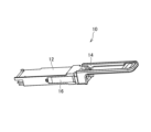
図1は、本発明を適用した第1の実施形態に係る光モジュール10の概略の外観図である。光モジュール10は光送受信機であり、金属ケース12と、プルタブ14と、スライダ16とを含む部品で外形が構成される。
[First embodiment]
FIG. 1 is a schematic external view of an
図2は光モジュール10が装着された光伝送装置18の構成を示す模式図である。光伝送装置18に、複数の光モジュール10が、電気コネクタ20によりそれぞれ装着されている。光伝送装置18は例えば大容量のルータやスイッチである。光伝送装置18は例えば交換機の機能を有しており、基地局などに配置される。光伝送装置18は、光モジュール10より受信用のデータ(受信用の電気信号)を取得し、回路基板22に搭載されるドライバIC24などを用いて、どこへ何のデータを送信するかを判断し、送信用のデータ(送信用の電気信号)を生成し、該当する光モジュール10へそのデータを伝達する。
FIG. 2 is a schematic diagram showing the configuration of the
光モジュール10は、プリント基板(Printed Circuit Board:PCB)26と、フレキシブル基板(FPC:Flexible Printed Circuits)28と、光信号と電気信号との変換を行うための複数の光サブアセンブリ30とを備える。具体的には、光サブアセンブリ30として、ROSA30AとTOSA30Bとを備えている。なお、ここでは、ROSA及びTOSAは、光送受信機能を有する双方向サブアセンブリ(BOSA:Bi-directional Optical SubAssembly)は:Transmitter Optical SubAssembly)を包含するものとする。なお、本実施形態の光モジュール10は送信機能と受信機能の両方を備えたトランシーバーであるが、本発明に係る光モジュールは送信機能のみ、つまりTOSAのみを備えたものであってもよい。
The
プリント基板26は柔軟性の無いリジッド基板である。プリント基板26と複数の光サブアセンブリ30とは、フレキシブル基板28を介して接続されている。ROSA30Aから電気信号がフレキシブル基板28を介してプリント基板26へ伝送される。また、プリント基板26から電気信号がフレキシブル基板28を介してTOSA30Bへ伝送される。光サブアセンブリ30が有する光変換素子は、光信号又は電気信号のうち一方から他方へ変換する素子である。電気信号を光信号へ変換する光変換素子は発光機能及び光変調機能を有し、ここでは光出力素子と呼ぶ。TOSA30Bは光出力素子を備える。一方、ROSA30Aは光信号を電気信号へ変換する光変換素子として受光素子を備える。光信号の入出力のために、光サブアセンブリ30には光ファイバ32が接続されている。
The printed
図3は、光モジュール10の金属ケース12内部に搭載される主要部品の構造を示す概略の斜視図である。光モジュール10は50Gbit/s級の光送受信機であり、例えばSFP56 MSA規格の光送受信機である。その主要部品は、ROSA30A、TOSA30B、プリント基板26及びフレキシブル基板28を含む。ROSA30Aとプリント基板26との間、及びTOSA30Bとプリント基板26との間はそれぞれ、可撓性を有したフレキシブル基板28で接続されている。つまり、ROSA30A及びTOSA30Bはそれぞれフレキシブル基板28の一方の端部に接続され、各フレキシブル基板28の他方の端部はプリント基板26に重なって電気的に接続されている。
FIG. 3 is a schematic perspective view showing the structure of the main components mounted inside the
TOSA30BはTO-CANパッケージで構成する。TO-CANパッケージを用いることで、TOSA30Bの小型化と低コスト化が図れる。図3には現れていないが、TO-CANパッケージの内部には光出力素子である半導体レーザLD1が1個搭載されている。フレキシブル基板28と半導体レーザLD1との間の伝送線路(図4の伝送線路56a,56b)として、TO-CANパッケージには、ステムの孔とリードピンとを含んで構成される一対の同軸線路が設けられる。
TOSA30B consists of a TO-CAN package. By using the TO-CAN package, the TOSA30B can be made smaller and lower in cost. Although not shown in FIG. 3, one semiconductor laser LD1, which is a light output element, is mounted inside the TO-CAN package. As a transmission line between the
プリント基板26は複数の層状の導電層と誘電体層で構成され、導電層には銅を用い、誘電体層にはガラス布基材とエポキシ樹脂からなる材料(ガラスエポキシ樹脂)を用いる。当該導電層によりプリント基板26には回路配線やグラウンドが形成される。プリント基板26には、それら導電層及び誘電体層を用いて、後述する差動伝送線路が形成される。また、プリント基板26には電子部品が実装され、ROSA30Aからの受信信号を処理する回路や、TOSA30Bを駆動する回路が構成される。図3にはプリント基板26表面に実装された電子部品として、TOSA30Bを駆動するための駆動IC34や、後述する抵抗素子Rm、コンデンサC1,C2が示されている。抵抗素子Rmは例えば0603サイズの表面実装型チップ抵抗とする。また、コンデンサC1,C2は例えば0603サイズの表面実装型チップコンデンサとする。
The printed
フレキシブル基板28は例えば、厚さ50マイクロメートル[μm]程度のポリイミドフィルムを絶縁層として用い、その両面に銅からなる導電層を配置した構成である。フレキシブル基板28には、それら導電層及び絶縁層を用いて、後述する差動伝送線路が形成される。
The
図4は第1の実施形態の光モジュール10の送信部40の概略の回路図である。送信部40は、TOSAに含まれる部分(TOSA部分)、フレキシブル基板28に形成される部分(FPC部分)、及びプリント基板26に形成される部分(PCB部分)を含む。TOSA部分には半導体レーザLD1が配置される。LD1は例えばDFB-LDとする。PCB部分には駆動IC34が配置される。駆動IC34は、半導体レーザLD1を駆動する電気信号を出力する駆動回路を含み、当該駆動回路は、差動信号を出力する出力段の回路として例えば、カレントモードロジック(Current mode Logic:CML)回路を有する。
FIG. 4 is a schematic circuit diagram of the transmitting
図4には駆動IC34の回路のうち当該CML回路を示している。CML回路41は、それぞれのベースを入力端子IN1,IN2としそれぞれのコレクタを出力端子OUT1,OUT2とするトランジスタTR1,TR2と、TR1,TR2双方のエミッタに共通に接続された定電流源42と、TR1,TR2それぞれのコレクタと電源電圧VCCとの間に接続され互いに同じ抵抗値を有する出力抵抗(プルアップ抵抗、あるいは内部終端抵抗)Rdとを含んで構成される。CML回路41は、一対の入力端子IN1,IN2に供給される差動入力信号の電位差に応じて、一対の出力端子OUT1,OUT2から出力信号として差動信号を出力する。
FIG. 4 shows the CML circuit among the circuits of the
図4の送信部40は、CML回路41の一対の出力端子OUT1,OUT2と半導体レーザLD1の一対の入力端子との間を接続する一対の伝送線路43a,43bからなる差動伝送線路43を有し、駆動IC34とLD1とを平衡接続する。差動伝送線路43により、出力端子OUT1,OUT2から出力される差動信号に応じた電流がLD1に供給され、LD1は当該差動信号に応じて変調された光信号を出力する。ちなみに、図4では、LD1の一対の入力端子を構成するアノードとカソードのうち、アノードが伝送線路43aにより出力端子OUT1に接続され、カソードが伝送線路43bにより出力端子OUT2に接続されている。
The
差動伝送線路43は、第1の特性インピーダンス(差動インピーダンスZdiff1)を有し駆動回路の一対の出力端子OUT1,OUT2に接続された第1差動伝送線路と、第1の特性インピーダンスより小さい第2の特性インピーダンス(差動インピーダンスZdiff2)を有しLD1の一対の入力端子に接続された第2差動伝送線路と、第1差動伝送線路と第2差動伝送線路とを直列につなぐ接続部とからなる。
The
ここでは、駆動IC34(CML回路41)の差動出力インピーダンスを100Ωとし、これに対応して差動インピーダンスZdiff1は100Ωとする。また、差動インピーダンスZdiff2は50Ωとする。なお、CML回路41の差動出力インピーダンスは基本的には出力抵抗Rdの抵抗値(以下、Rdとする)の2倍となるので、RdとZdiff1とをRd=Zdiff1/2を満たす関係として、CML回路41と第1差動伝送線路とのインピーダンス整合を図ることができる。つまり、例えば、Rdを50Ωに設定することで、Zdiff1が100Ωの差動伝送線路43とのインピーダンス整合が実現される。
Here, the differential output impedance of the drive IC 34 (CML circuit 41) is set to 100Ω, and correspondingly, the differential impedance Z diff1 is set to 100Ω. Further, the differential impedance Z diff2 is assumed to be 50Ω. Note that the differential output impedance of the
接続部には抵抗素子Rmが配置される。具体的には、抵抗素子Rmはその両端を、伝送線路43aにおける接続部44aと伝送線路43bにおける接続部44bとに接続される。この抵抗素子Rmを備えた接続部の構成は、第1差動伝送線路と第2差動伝送線路とのインピーダンスのギャップに伴う問題を解決するものであり、これについては後に反射吸収回路として説明する。
A resistance element Rm is arranged at the connection portion. Specifically, both ends of the resistance element Rm are connected to a connecting
伝送線路43a,43bには直流遮断用コンデンサC1,C2を直列に挿入することができる。なお、コンデンサC1,C2の容量値は例えば0.1マイクロファラッド[μF]程度とすることができる。コンデンサC1,C2のLD1側の端子には、LD1にバイアス電流を供給するバイアス回路45a,45bを接続することができる。具体的には、バイアス回路45aは電源V_anodeと伝送線路43aとの間に設けられ、バイアス回路45bは電源V_cathodeと伝送線路43bとの間に設けられる。また、伝送線路43a,43bのコンデンサC1,C2より駆動回路側に、バイアス回路46a,46bを接続することができる。本実施形態では、バイアス回路46a,46bと伝送線路43a,43bとの接続位置は、接続部44a,44bと駆動回路との間とし、当該位置にて、バイアス回路46aは電源VCCと伝送線路43aとの間に設けられ、バイアス回路46bは電源VCCと伝送線路43bとの間に設けられる。これらバイアス回路45a,45b,46a,46bは差動伝送線路43の特性に影響しない、あるいは影響を最小限にするように、インピーダンスが充分に高くなるように設計する。例えばインダクタ、フェライトビーズ、抵抗の組み合わせで構成して良い。
DC blocking capacitors C1 and C2 can be inserted in series in the
本実施形態では差動伝送線路43に、駆動IC34側から半導体レーザLD1側へ向かう順序で並ぶ6つの区間S1~S6(不図示)を定義する。このうち区間S1~S4はPCB部分に属する。区間S1は駆動IC34の出力端子OUT1,OUT2からバイアス回路46a,46bの接続位置までの区間である。また、区間S2はバイアス回路46a,46bの接続位置から接続部44a,44bまでの区間、区間S3は接続部44a,44bからコンデンサC1,C2の一方端までの区間である。そして、区間S4はコンデンサC1,C2の他方端からプリント基板26とフレキシブル基板28との境界までの区間である。区間S5はFPC部分である。区間S6はTOSA部分であり、TOSA30Bのフレキシブル基板28との接続位置からLD1のアノード、カソードまでの区間である。
In this embodiment, six sections S1 to S6 (not shown) are defined in the
本実施形態では、伝送線路43aの区間S1~S6に属する部分を図4に示すように伝送線路51a~56a、また伝送線路43bの区間S1~S6に属する部分を図4に示すように伝送線路51b~56bと表す。つまり、伝送線路43aには、伝送線路51a,52a、接続部44a、伝送線路53a、コンデンサC1、伝送線路54a,55a,56aが直列に接続され、伝送線路43bには、伝送線路51b,52b、接続部44b、伝送線路53b、コンデンサC2、伝送線路54b,55b,56bが直列に接続される。ここで、伝送線路43a,43bには当該伝送線路に直列に接続された抵抗素子が配置されていないことに留意する。
In this embodiment, the portions of the
差動伝送線路43は、半導体レーザLD1を駆動する高周波の電気信号を伝送可能に構成される。例えば、PCB部分にある区間S1~S4の差動伝送線路43(伝送線路51a~54a,51b~54b)は、プリント基板26の導電層及び誘電体層を用いて構成されたマイクロストリップライン(Microstripline)であり、同様に、FPC部分にある区間S5の差動伝送線路43(伝送線路55a,55b)は、フレキシブル基板28の導電層及び誘電体層を用いて構成されたマイクロストリップラインである。なお、これらPCB部分、FPC部分の差動伝送線路43はストリップライン(Stripline)、あるいはコプラナ導波路(Coplanar Waveguide)で構成しても良い。
The
TOSA部分にある区間S6の差動伝送線路43(伝送線路56a,56b)は、既に述べたように、TO-CANパッケージのステムの孔とリードピンとを含んで構成される一対の同軸線路であり、基本的にTO-CANパッケージ内に配置される。なお、このTOSA部分の差動伝送線路43はマイクロストリップラインやストリップラインで構成しても良い。
As already mentioned, the differential transmission line 43 (
差動伝送線路43のうち、第1差動伝送線路に属する区間S1の部分(伝送線路51a,51b)及び区間S2の部分(伝送線路52a,52b)の差動インピーダンスはZdiff1に設定され、一方、第2差動伝送線路に属する区間S3の部分(伝送線路53a,53b)、区間S4の部分(伝送線路54a,54b)、区間S5の部分(伝送線路55a,55b)、区間S6の部分(伝送線路56a,56b)の差動インピーダンスはZdiff2に設定される。
Of the
第1差動伝送線路及び第2差動伝送線路とそれらの接続部44a,44bの間に設けた抵抗素子Rmとは、第2差動伝送線路の側から第1差動伝送線路の側に向かう電気信号に対する反射係数Γを低減する反射吸収回路を構成する。つまり、第1差動伝送線路と第2差動伝送線路との接続部でのインピーダンスのギャップは、第2差動伝送線路の側から第1差動伝送線路の側へ向かう信号に対して反射を生じ得るが、抵抗素子Rmを配置することで当該反射を小さくする。例えば、駆動IC34からの駆動信号が半導体レーザLD1の入力端子で反射されて、第2差動伝送線路の側から第1差動伝送線路の側へ戻る信号成分が生じるが、抵抗素子Rmを含んで構成される反射吸収回路を設けることで、当該信号成分が再び反射されてLD1へ向かうことによる多重反射が低減される。
The resistance element Rm provided between the first differential transmission line and the second differential transmission line and their
ここでは便宜上、差動伝送線路43にて接続部44a,44bの両側それぞれ1区間までを反射吸収回路60と考えることにする。つまり、反射吸収回路60は、第1差動伝送線路のうち接続部44a,44bに隣接する1つの区間Sαと、第2差動伝送線路のうち接続部44a,44bに隣接する1つの区間Sβと、接続部44a,44b及び当該接続部間を結ぶように配置した抵抗素子Rmとからなる。
Here, for convenience, up to one section on each side of the connecting
図5は反射吸収回路60の構造を示す模式的な平面図である。図5において上側が半導体レーザLD1に向かう側であり、下側が駆動IC34に向かう側である。本実施形態では反射吸収回路60はプリント基板26に配置される。区間Sα,Sβの差動伝送線路43はマイクロストリップラインであり、マイクロストリップラインは、基板表層の導電体からなるストリップ導体と、それらの下に配置した誘電体層と、当該誘電体層の下に平面的に配置した接地導体層とで構成される。具体的には、反射吸収回路60は区間Sαの伝送線路を構成するストリップ導体61a,61bと区間Sβの伝送線路を構成するストリップ導体62a,62bとを有する。各ストリップ導体は信号の伝送方向に沿って細長く延びた平面形状であり、ストリップ導体61a,61bはそれぞれの幅がW1で、互いの間に間隔G1を有して平行に延在し、ストリップ導体62a,62bはそれぞれの幅がW2で、間隔G2を有して平行に延在する。一方、接地導体層は、ストリップ導体に対向する領域だけでなく、さらにその両側に広がる領域にも形成され、例えば、基板全面に亘って形成される。
FIG. 5 is a schematic plan view showing the structure of the reflection/
ストリップ導体の厚さは例えば37μmとする。また、誘電体層の厚さ、すなわちストリップ導体を構成する表層の導電層と接地導体層との距離は60μmとし、誘電体層の比誘電率は3.5とする。ストリップ導体61a,61b及びストリップ導体62a,62bの寸法は、電磁界解析ツールなどを用いることで比較的容易に設計し、所望の特性インピーダンス値を得ることができる。本実施形態では、一例として,ストリップ導体61a,61bの間隙G1を0.25ミリメートル[mm]、幅W1を0.11mmとすることで区間Sαの差動伝送線路43の差動インピーダンスZdiff1を100Ωにしている。またストリップ導体62a,62bの間隙G2を0.25mm、幅W2を0.34mmとすることで区間Sβの差動伝送線路43の差動インピーダンスZdiff2を50Ωにしている。
The thickness of the strip conductor is, for example, 37 μm. Further, the thickness of the dielectric layer, that is, the distance between the surface conductive layer constituting the strip conductor and the ground conductor layer, is 60 μm, and the dielectric constant of the dielectric layer is 3.5. The dimensions of the
本実施形態では、区間Sαは区間S2であり、ストリップ導体61a,61bは伝送線路52a,52bに対応する。また、区間Sβは区間S3であり、ストリップ導体62a,62bは伝送線路53a,53bに対応する。なお、区間S2と同じくプリント基板26上の第1差動伝送線路である区間S1については、伝送線路51a,51bのストリップ導体を区間S2と共通の幅・間隔として100ΩのZdiff1に設定することができ、区間S3と同じくプリント基板26上の第2差動伝送線路である区間S4については、伝送線路54a,54bのストリップ導体を区間S3と共通の幅・間隔として50ΩのZdiff2に設定することができる。また、フレキシブル基板28上のマイクロストリップライン、具体的には区間S5の差動伝送線路についても、基板の導電層・誘電体層の厚みや比誘電率がプリント基板26とは異なり得ることに留意した上で、プリント基板26上の差動伝送線路と同様の手法でストリップ導体の寸法を設計し、50ΩのZdiff2を得ることができる。
In this embodiment, the section Sα is the section S2, and the
接続部44a,44bにおけるストリップ導体は、伝送線路を構成すると共に、抵抗素子Rmの端子を接続するパッドとなる。そのため、接続部44a,44bにおけるストリップ導体の幅W、長さL、形状は当該パッドの位置やサイズなどに配慮して定められる。
The strip conductors in the connecting
例えば、抵抗素子Rmを0603サイズの表面実装型チップ抵抗とし、これを接続部44a,44b間に接続する場合、抵抗素子Rmの配置領域は長さLの方向に0.3mm、幅Wの方向に0.6mmの大きさとなる。ここで、ストリップ導体の幅W方向に沿った抵抗素子Rmの寸法0.6mmは、区間Sαにおけるストリップ導体61a,61bの配置幅(2・W1+G1)である0.47mmより大きく、区間Sβにおけるストリップ導体62a,62bの配置幅(2・W2+G2)である0.93mmより小さい。よって、単純には、接続部44a,44bは、それぞれのストリップ導体の幅Wを0.175mm、間隔Gを0.25mm、長さLを0.3mmとすることで、抵抗素子Rmの配置領域に適合すると共に、区間Sαと区間Sβとの間でストリップ導体の幅の変化に合わせて差動インピーダンスも漸次変化する構成とすることができる。
For example, when the resistance element Rm is a 0603 size surface-mounted chip resistor and is connected between the
図5に示す構成ではさらに、接続部のストリップ導体のパターンを、抵抗素子Rmのパッドと区間Sα,Sβそれぞれとの間でストリップ導体の幅が連続的に変化するようにしている。具体的には、接続部44a,44bは長さL方向に関して、区間Sα側に抵抗素子Rmの配置領域より拡張された部分を含み、当該部分にてストリップ導体の幅WをW1から抵抗素子Rmのパッドの配置に応じた値まで連続的に単調増加させる。また、長さL方向に関して、抵抗素子Rmのパッドの途中の位置から区間Sβへ向けて、ストリップ導体の幅Wを抵抗素子Rmのパッドの配置に応じた値からW2まで連続的に単調増加させる。
In the configuration shown in FIG. 5, the strip conductor pattern of the connecting portion is further configured so that the width of the strip conductor changes continuously between the pad of the resistive element Rm and each of the sections Sα and Sβ. Specifically, in the length L direction, the connecting
半導体レーザLD1側から見た場合の反射吸収回路60の反射係数Γは、抵抗素子Rmの抵抗値をRとすると次式で与えられる。
The reflection coefficient Γ of the reflection/

図6は本実施形態の光モジュール10の送信部40における反射吸収回路60の半導体レーザLD1側から見た差動反射特性を示すグラフである。当該グラフの横軸Rは抵抗素子Rmの抵抗値である。また、縦軸Sdd22は半導体レーザLD1側から反射吸収回路60へ入射した信号に対する反射信号の強度に関するSパラメータをデシベル[dB]で表示しており、当該Sdd22は式(1)で計算されたΓで与えられる。
FIG. 6 is a graph showing the differential reflection characteristics of the reflection/
実験に基づく検討により、Sdd22が-20dB以下であれば、不要な電気波形の多重反射による半導体レーザ入力信号の乱れを抑制することができ、充分に良好な光出力波形を得ることができた。このSdd22≦-20dBは|Γ|≦0.1に該当する。よって、抵抗素子Rmの抵抗値Rは、第2差動伝送線路の側から第1差動伝送線路の側に向かう信号に対する反射係数Γの絶対値を0.10以下にする値に設定する。 Experimental studies have shown that when Sdd22 is -20 dB or less, it is possible to suppress the disturbance of the semiconductor laser input signal due to multiple reflections of unnecessary electrical waveforms, and it is possible to obtain a sufficiently good optical output waveform. This Sdd22≦−20 dB corresponds to |Γ|≦0.1. Therefore, the resistance value R of the resistance element Rm is set to a value that makes the absolute value of the reflection coefficient Γ for the signal traveling from the second differential transmission line side to the first differential transmission line side 0.10 or less.
Zdiff1=100Ω、Zdiff2=50Ωの差動伝送線路43において、抵抗素子Rmの抵抗値Rを69.4Ω~157.1Ωとしたときに|Γ|≦0.1とすることができ、特にR=100Ωとしたとき理論的にΓ=0、つまり無反射とすることができる。よって、Zdiff1=100Ω、Zdiff2=50Ωの差動伝送線路43においては、Rは69.4Ω~157.1Ωの範囲にて選択することができ、また、できるだけ100Ωに近い値に設定するのが好適である。
In the
図7は、図5に示した反射吸収回路60において、抵抗素子Rmの抵抗値Rを100Ωとした場合の差動小信号特性を示したグラフであり、横軸が周波数、縦軸がSパラメータである。この特性は電磁界解析ツールにより算出したものであり、図5において下側(駆動IC34に向かう側)に差動ポート1を配置し、上側(半導体レーザLD1に向かう側)に差動ポート2を配置している。差動ポート1の差動インピーダンスは100Ωで正規化し、差動ポート2の差動インピーダンスは50Ωで正規化している。
FIG. 7 is a graph showing the differential small signal characteristics when the resistance value R of the resistor element Rm is 100Ω in the reflection/
図7に示すように、半導体レーザLD1側から見込んだ差動反射係数Sdd22は0~60ギガヘルツ[GHz]と広い周波数範囲において-28dB以下と十分小さく抑えられており、プリント基板26上のマイクロストリップラインと、チップ抵抗である抵抗素子Rmとにより構成した反射吸収回路60により、非常に良好な反射吸収回路を実現できることを示している。
As shown in FIG. 7, the differential reflection coefficient Sdd22 seen from the side of the semiconductor laser LD1 is kept sufficiently small at -28 dB or less in a wide frequency range of 0 to 60 gigahertz [GHz], and the microstrip on the printed
また、図7は、駆動IC34側から見込んだ差動反射係数Sdd11が-6dB程度であり、反射吸収回路60のこの向きにおける反射を抑える機能は弱いことを示しているが、一方、差動通過特性Sdd21は-3dB程度であり、駆動IC34の差動駆動信号が反射吸収回路60を通過したときの損失量を3dB程度と比較的低く抑えられることができ、かつ当該損失量を0~60GHzと広い周波数範囲においてほぼ一定値に保てることを示している。
Further, FIG. 7 shows that the differential reflection coefficient Sdd11 seen from the
図8は、プリント基板26上に構成した図5の反射吸収回路60を図4の光モジュール10の送信部40の反射吸収回路として適用した場合についての送信部40の各部における電流波形のアイ・ダイアグラムである。図8(a),(b),(C)はそれぞれ図4の回路図に示す位置PA,PB,PCでの波形である。位置PAは半導体レーザLD1のアノード端子であり、また、位置PBは反射吸収回路60の出力(半導体レーザLD1側)の端子、位置PCは反射吸収回路60の入力(駆動IC34側)の端子である。
FIG. 8 shows the eye and current waveforms of current waveforms in each part of the transmitting
図8は回路シミュレータによる結果であり、反射吸収回路60の回路パラメータには、電磁界解析ツールにより算出した図7の小信号特性(4ポートのSパラメータ)の結果を適用している。また、駆動IC34の変調信号は、変調方式をNRZ(Non-return-to-zero)、ビットレートを10.7Gbit/sとした。
FIG. 8 shows the results obtained using a circuit simulator, and the results of the small signal characteristics (4-port S parameters) shown in FIG. 7 calculated using an electromagnetic field analysis tool are applied to the circuit parameters of the reflection/
位置PBでは、半導体レーザLD1に向かう進行波と、LD1側からくる逆向きの波とが存在する。この逆向きの波は半導体レーザLD1に向かう進行波に対する反射波であり、差動インピーダンスZdiff2が50Ωである第2差動伝送線路とそれよりもインピーダンスが低い半導体レーザLD1とのインピーダンス不整合により生じる。PBではこれら進行波と反射波とが重なり、図8(b)に示すように複雑な電流波形が生じている。 At position PB , there are a traveling wave toward the semiconductor laser LD1 and a wave in the opposite direction coming from the LD1 side. This wave in the opposite direction is a reflected wave of the traveling wave toward the semiconductor laser LD1, and is due to the impedance mismatch between the second differential transmission line whose differential impedance Z diff2 is 50Ω and the semiconductor laser LD1 whose impedance is lower than that. arise. At P B, these traveling waves and reflected waves overlap, resulting in a complicated current waveform as shown in FIG. 8(b).
一方、図8(a)は位置PA、つまり半導体レーザのアノード端子における電流波形である。上記位置PBで見られた反射波は、その先の反射吸収回路60で充分に吸収され、第1差動伝送線路と第2差動伝送線路との不整合による再反射が抑圧される。そのため、位置PAでは図8(a)に示すように、再反射波による波形の乱れは抑制され、ジッタ成分やノイズ成分の少ない良好な電流波形が得られている。ここで、半導体レーザLD1としてDFB-LDを用いる場合、入力であるダイオードの順方向電流値と出力であるレーザ光強度とは良い線形性を持つ。よって、ダイオードに流れる電流波形が良好であれば、光送信機の出力として良好なレーザ光波形が得られる。このように、本実施形態の光モジュール10によれば、半導体レーザへの信号の減衰量を最小にしつつ、良好な電流波形を得る、すなわち良好な光出力波形を得ることが可能である。
On the other hand, FIG. 8(a) shows the current waveform at the position P A , that is, the anode terminal of the semiconductor laser. The reflected wave seen at the position PB is sufficiently absorbed by the reflection/
なお、位置PCでは、駆動IC34からの進行波と半導体レーザLD1からの反射波に加え、反射吸収回路60の入力側からの反射波が存在し、それらが重なることで、図8(c)に示すように、図8(b)と比べて更に複雑な電流波形が生じている。
Note that at position PC , in addition to the traveling wave from the
以上説明した本実施形態によれば、差動出力インピーダンスが100Ωの駆動ICと伝送線路の差動インピーダンスが50ΩのTO-CANパッケージを用いたTOSAとを利用でき、かつ駆動ICと半導体レーザとの間での電気信号の多重反射を抑圧し、半導体レーザへの信号の減衰量を最小にして、良好な光出力波形を得ることができる。これによりTOSAのパッケージの小型化と低コスト化を両立した光モジュール10を提供することができる。
According to this embodiment described above, it is possible to use a drive IC with a differential output impedance of 100Ω and a TOSA using a TO-CAN package with a transmission line differential impedance of 50Ω, and to connect the drive IC and the semiconductor laser. By suppressing multiple reflections of electrical signals between the semiconductor lasers and minimizing the amount of signal attenuation to the semiconductor laser, it is possible to obtain a good optical output waveform. As a result, it is possible to provide an
なお、本実施形態では、駆動IC34の一対の差動出力インピーダンスは一例として100Ωとしたが、この値に限定されない。例えば、駆動IC34の一対の差動出力インピーダンスが80Ωである場合には、第1差動伝送線路の差動インピーダンスZdiff1は80Ω、また第2差動伝送線路の差動インピーダンスZdiff2は50Ωとし、反射吸収回路60の抵抗素子Rmの抵抗値Rは、|Γ|≦0.1とするために83.7Ω~258.2Ωの範囲にて選択することができ、また、できるだけ133.3Ωに近い値に設定するのが好適である。
Note that in this embodiment, the pair of differential output impedances of the
[第2の実施形態]
本発明の第2の実施形態は送信部40の回路、特に差動伝送線路43の構成に第1の実施形態との違いを有する。両実施形態はその他の点では基本的に共通であり、例えば、図1~図3は本実施形態に援用される。
[Second embodiment]
The second embodiment of the present invention differs from the first embodiment in the circuit of the
図9は第2の実施形態に係る光モジュール10の送信部40の概略の回路図である。この回路について、図4の第1の実施形態の回路との相違点を中心に説明する。主たる相違点は端的には、反射吸収回路60がフレキシブル基板28に配置されていることである。
FIG. 9 is a schematic circuit diagram of the transmitting
本実施形態では差動伝送線路43に、駆動IC34側から半導体レーザLD1側へ向かう順序で並ぶ7つの区間S1~S7(不図示)を定義する。このうち区間S1~S4はPCB部分に属する。区間S1は駆動IC34の出力端子OUT1,OUT2からバイアス回路46a,46bの接続位置までの区間である。区間S2はバイアス回路46a,46bの接続位置からコンデンサC1,C2の一方端までの区間である。区間S3はコンデンサC1,C2の他方端からバイアス回路45a,45bの接続位置までの区間、区間S4はバイアス回路45a,45bの接続位置からプリント基板26とフレキシブル基板28との境界までの区間である。区間S5,S6はFPC部分に属する。区間S5はプリント基板26との境界から接続部44a,44bまでの区間であり、区間S6は接続部44a,44bからTOSA30Bとの境界までの区間である。そして、区間S7はTOSA部分であり、TOSA30Bのフレキシブル基板28との接続位置からLD1のアノード、カソードまでの区間である。
In this embodiment, seven sections S1 to S7 (not shown) are defined in the
本実施形態では、伝送線路43aの区間S1~S7に属する部分を図9に示すように伝送線路71a~77a、また伝送線路43bの区間S1~S7に属する部分を図9に示すように伝送線路71b~77bと表す。つまり、伝送線路43aには、伝送線路71a,72a、コンデンサC1、伝送線路73a,74a,75a、接続部44a、伝送線路76a,77aが直列に接続され、伝送線路43bには、伝送線路71b,72b、コンデンサC2、伝送線路73b,74b,75b、接続部44b、伝送線路76b,77bが直列に接続される。ここで、伝送線路43a,43bには第1の実施形態と同様、抵抗素子は直列に配置されていない。
In this embodiment, the portions of the
例えば、PCB部分及びFPC部分の区間S1~S6の差動伝送線路43(伝送線路71a~76a,71b~76b)は第1の実施形態と同様、マイクロストリップラインで構成されるが、ストリップラインやコプラナ導波路(Coplanar Waveguide)で構成しても良い。また、TOSA部分にある区間S7の差動伝送線路43(伝送線路77a,77b)は、第1の実施形態の区間S6と同様に構成される。
For example, the differential transmission lines 43 (
差動伝送線路43のうち、区間S1~S5の部分(伝送線路71a~75a,71b~75b)が、差動インピーダンスZdiff1の第1差動伝送線路をなし、区間S6,S7の部分(伝送線路76a,77a,76b,77b)が、差動インピーダンスZdiff2の第2差動伝送線路をなす。なお、例えば、第1の実施形態と同様、Zdiff1は100Ω、Zdiff2は50Ωである。
Of the
上述したように本実施形態では反射吸収回路60はフレキシブル基板28に配置される。具体的には、図5に示した構造がフレキシブル基板28に形成され、本実施形態では区間S5,S6がそれぞれ図5の区間Sα,Sβに対応する。つまり、図5のストリップ導体61a,61bは図9の伝送線路75a,75bに対応し、ストリップ導体62a,62bは伝送線路76a,76bに対応する。なお、区間Sα,Sβ及び接続部44a,44bのストリップ導体の幅や間隔などは、第1の実施形態のプリント基板26での値とは異なり得、フレキシブル基板28での導電層・誘電体層の厚みや比誘電率に基づいて設計される。一方、接続部44a,44bの間に配置される抵抗素子Rmの抵抗値Rは、Zdiff1,Zdiff2に基づいて第1の実施形態と同様に設定される。具体的には、|Γ|≦0.1となるように設定され、Zdiff1=100Ω、Zdiff2=50Ωの場合にはRは69.4Ω~157.1Ωの範囲にて選択することができる。
As described above, in this embodiment, the reflection/
ここで説明した第2の実施形態によっても第1の実施形態で述べた効果が得られる。すなわち、差動出力インピーダンスが100Ωの駆動ICと伝送線路の差動インピーダンスが50ΩのTO-CANパッケージを用いたTOSAとを利用でき、かつ駆動ICと半導体レーザとの間での電気信号の多重反射を抑圧し、半導体レーザへの信号の減衰量を最小にして、良好な光出力波形を得ることができる。これによりTOSAのパッケージの小型化と低コスト化を両立した光モジュール10を提供することができる。
The second embodiment described here also provides the effects described in the first embodiment. In other words, it is possible to use a TOSA using a TO-CAN package with a drive IC with a differential output impedance of 100Ω and a transmission line with a differential impedance of 50Ω, and multiple reflections of electrical signals between the drive IC and the semiconductor laser. It is possible to suppress the amount of signal attenuation to the semiconductor laser and obtain a good optical output waveform. As a result, it is possible to provide an
さらに第2の実施形態によれば、反射吸収回路60をフレキシブル基板28に配置するので、フレキシブル基板28の設計及び作製のみで、反射吸収回路60についての試作検討をより短期に行うことができるという利点が生じる。
Furthermore, according to the second embodiment, since the reflection/
なお、本実施形態では、バイアス回路45a,45bによる電流供給点を直流遮断用のコンデンサC1,C2と接続部44a,44bとの間に配置しているので、これらバイアス回路45a,45bから半導体レーザLD1に供給するバイアス電流が抵抗素子Rmにも流れ、その分、消費電力が増大する。よって、抵抗値Rは、|Γ|の低減という観点に加え、消費電力の低減を考慮して選択してもよい。例えばZdiff1=100Ω、Zdiff2=50Ωの場合にて、|Γ|≦0.1となる69.4Ω~157.1Ωの範囲にて抵抗値Rを選択する際、R=100Ωに近づけて|Γ|を小さくする効果と、Rを大きくして低消費電力化を図る効果とを考慮する。例えば、この双方を考慮し、第2の実施形態でのRの選択範囲は、100Ωより小さい範囲を除外し、100Ω~157.1Ωに限定することもできる。
In this embodiment, since the current supply points by the
[第3の実施形態]
本発明の第3の実施形態は送信部40の回路、特に差動伝送線路43の構成に第1、第2の実施形態との違いを有する一方、その他の点では基本的に第1、第2の実施形態と共通であり、例えば、図1~図3は本実施形態にも援用される。
[Third embodiment]
The third embodiment of the present invention is different from the first and second embodiments in the circuit of the
本実施形態の差動伝送線路43は、第2の実施形態における差動伝送線路43のうち、フレキシブル基板28上にあった区間S6の伝送線路76a,76bを省略した構成である。図10は第3の実施形態の差動伝送線路43のうち第2の実施形態との差異が存在する部分の概略の回路図であり、FPC部分とTOSA部分を示している。なお、本実施形態の差動伝送線路43のPCB部分は第2の実施形態にて示した図9のPCB部分と共通とすることができる。
The
本実施形態では、抵抗素子Rmが配置された接続部44a,44b及びその両側の区間Sα,Sβの差動伝送線路からなる反射吸収回路60のうち、区間Sαの第1差動伝送線路をなす伝送線路75a,75bと、接続部44a,44b及び抵抗素子Rmとがフレキシブル基板28に配置され、区間Sβの第2差動伝送線路はTOSA30B内の伝送線路77a,77bからなる。
In this embodiment, of the reflection/
伝送線路75a,75b及び接続部44a,44bは第2の実施形態と同様、フレキシブル基板28上に例えばマイクロストリップラインで形成される。伝送線路77a,77bは、第1の実施形態の区間S6又は第2の実施形態の区間S7と同様、TOSA30Bのパッケージ内に設けられた同軸線路で構成される。なお、例えば、第1、第2の実施形態と同様、Zdiff1は100Ω、Zdiff2は50Ωとする。
The
伝送線路77a,77bは、例えば外径0.7mm、内径0.3mmの同軸線路とし、誘電体として比誘電率4.1のガラス材を用い、同軸線路の長さ、すなわちTOSA30Bの金属パッケージをなすステムの厚さを1.2mmとすることにより、差動インピーダンスZdiff2が50Ωの差動伝送線路を構成できる。この差動伝送線路の電気長を算出すると、周波数31GHzにおいて1/4波長に相当する。ここで、半導体レーザLD1としてDFB-LDを用いた場合、順方向電流バイアス時の微分抵抗、すなわち差動インピーダンスは6~8Ωと比較的に小さい。一方、周波数31GHzにおいて、伝送線路77a,77bからなる差動伝送線路は1/4波長インピーダンス変成器として機能するので、当該周波数付近ではTOSA30Bを外部から見込んだ場合のインピーダンスは充分に高くなる。これにより駆動IC34から半導体レーザLD1側を見込んだときは抵抗素子Rmのインピーダンスが支配的となる。
The
よって本実施形態の反射吸収回路60によれば、抵抗素子Rmを100Ωとすることにより、差動反射特性Sdd11を周波数31GHz付近で整合状態に近づけることができる。つまり、本実施形態の光モジュール10は、特に変調レートが25~28Gbit/sの光送受信機において通常は抑圧するのが難しい高周波領域における不要な多重反射による電気波形の乱れを軽減することができ、良好な光波形を得るに好適であるという利点を有する。
Therefore, according to the reflection/
図11は、本実施形態における反射吸収回路60の入力側から半導体レーザLD1を見た差動反射特性Sdd11の周波数特性を示すグラフである。抵抗素子Rmの抵抗値Rが100Ωの場合、周波数31GHz付近でSdd11は-20dB以下の値を示し、また周波数範囲25GHzから38GHzでも-10dB以下の良好な値が得られている。抵抗素子Rmの抵抗値Rはこれに限るものではなく、例えば抵抗値Rを116Ωにすることで,周波数31GHz付近の反射を更に小さくできる。
FIG. 11 is a graph showing the frequency characteristics of the differential reflection characteristic Sdd11 when looking at the semiconductor laser LD1 from the input side of the reflection/
[第4の実施形態]
上記各実施形態では、光出力素子は直接変調方式の半導体レーザLD1とし、一例としてDFB-LDを用いた構成を説明した。しかし、半導体レーザはこれに限定されず、他の種類の直接変調方式の半導体レーザとしても良く、例えば、ファブリペロー型半導体レーザや、垂直共振器面発光レーザ(Vertical Cavity Surface Emitting LASER:VSCEL)などを用いてもよい。
[Fourth embodiment]
In each of the above embodiments, the optical output element is the direct modulation type semiconductor laser LD1, and the configuration using the DFB-LD as an example has been described. However, the semiconductor laser is not limited to this, and other types of direct modulation semiconductor lasers may be used, such as Fabry-Perot semiconductor lasers, vertical cavity surface emitting lasers (VSCEL), etc. may also be used.
また、光出力素子には外部変調方式の集積型半導体レーザを用いても良く、例えば、上記各実施形態における半導体レーザLD1に替えて外部変調方式の集積型半導体レーザLD2を用いた構成とすることができる。本発明の第4の実施形態はその半導体レーザLD2を用いた構成の一例である。以下、第4の実施形態について上記実施形態との相違点を中心に説明する一方、共通点については基本的に説明を省略する。例えば、図1~図3は本実施形態にも援用される。 Further, an external modulation type integrated semiconductor laser may be used as the optical output element. For example, an external modulation type integrated semiconductor laser LD2 may be used instead of the semiconductor laser LD1 in each of the above embodiments. I can do it. The fourth embodiment of the present invention is an example of a configuration using the semiconductor laser LD2. Hereinafter, the fourth embodiment will be described with a focus on differences from the above embodiments, while descriptions of common features will be basically omitted. For example, FIGS. 1 to 3 are also used in this embodiment.
図12は第4の実施形態に係る光モジュール10の送信部40の概略の回路図である。この回路は第2の実施形態の送信部40にLD2を適用した構成である。つまり、この回路の第2の実施形態との基本的な相違点は、TOSA30Bが半導体レーザLD1に替えて外部変調方式の集積型半導体レーザLD2を搭載している点にある。LD2は発光素子と光変調器とを集積した素子である。発光素子はDFB-LDとし、光変調器は例えば電界吸収型(Electroabsorption:EA)変調器とする。LD2では、DFB-LDは一定の強度のレーザ光を出力し、光変調器は当該レーザ光を変調して外部に出力する。そのため、差動伝送線路43は駆動IC34の出力端子OUT1,OUT2と光変調器とを接続し、駆動IC34から出力される変調信号が光変調器に入力される。具体的には、光変調器のアノード端子、カソード端子がそれぞれ伝送線路77a(伝送線路43a)、伝送線路77b(伝送線路43b)に接続される。
FIG. 12 is a schematic circuit diagram of the
一方、DFB-LDはバイアス回路から電流を供給されて発光する。バイアス回路はプリント基板26に形成された部分80とTOSA30B内のインダクタ81とからなり、電源V_LDから生成した電流をDFB-LDのアノードに供給する。
On the other hand, the DFB-LD emits light by being supplied with current from the bias circuit. The bias circuit consists of a
なお、DFB-LDのカソードは光変調器のカソードと共通に形成され、当該カソードとDFB-LDのアノードとの間にデカップリングコンデンサとしてコンデンサC3が接続される。また、光変調器のアノードとカソードとの間には抵抗素子Rtが接続され終端抵抗として機能する。 Note that the cathode of the DFB-LD is formed in common with the cathode of the optical modulator, and a capacitor C3 is connected as a decoupling capacitor between the cathode and the anode of the DFB-LD. Further, a resistive element Rt is connected between the anode and cathode of the optical modulator and functions as a terminating resistor.
ここで説明した第4の実施形態によっても第1の実施形態で述べた効果が得られる。すなわち、差動出力インピーダンスが100Ωの駆動ICと伝送線路の差動インピーダンスが50ΩのTO-CANパッケージを用いたTOSAとを利用でき、かつ駆動ICと半導体レーザとの間での電気信号の多重反射を抑圧し、半導体レーザへの信号の減衰量を最小にして、良好な光出力波形を得ることができる。これによりTOSAのパッケージの小型化と低コスト化を両立した光モジュール10を提供することができる。
The fourth embodiment described here also provides the effects described in the first embodiment. In other words, it is possible to use a TOSA using a TO-CAN package with a drive IC with a differential output impedance of 100Ω and a transmission line with a differential impedance of 50Ω, and multiple reflections of electrical signals between the drive IC and the semiconductor laser. It is possible to suppress the amount of signal attenuation to the semiconductor laser and obtain a good optical output waveform. As a result, it is possible to provide an
なお、本発明は、上述した各実施形態に限定されるものではなく種々の変形が可能である。例えば、実施形態で説明した構成は、実質的に同一の構成、同一の作用効果を奏する構成又は同一の目的を達成することができる構成で置き換えることができる。 Note that the present invention is not limited to the embodiments described above, and various modifications are possible. For example, the configuration described in the embodiment can be replaced with a configuration that is substantially the same, a configuration that has the same effect, or a configuration that can achieve the same purpose.
10 光モジュール、12 金属ケース、14 プルタブ、16 スライダ、18 光伝送装置、20 電気コネクタ、22 回路基板、24 ドライバIC、26 プリント基板、28 フレキシブル基板、30 光サブアセンブリ、30A ROSA、30B TOSA、32 光ファイバ、34 駆動IC、40 送信部、41 CML回路、42 定電流源、43 差動伝送線路、43a,43b,51a~56a,51b~56b,71a~77a,71b~77b 伝送線路、44a,44b 接続部、45a,45b,46a,46b,80 バイアス回路、60 反射吸収回路、61a,61b,62a,62b ストリップ導体、81 インダクタ、C1,C2,C3 コンデンサ、Rd 出力抵抗、Rm,Rt 抵抗素子、LD1,LD2 半導体レーザ。 10 optical module, 12 metal case, 14 pull tab, 16 slider, 18 optical transmission device, 20 electrical connector, 22 circuit board, 24 driver IC, 26 printed circuit board, 28 flexible board, 30 optical subassembly, 30A ROSA, 30B TOSA, 32 optical fiber, 34 drive IC, 40 transmitter, 41 CML circuit, 42 constant current source, 43 differential transmission line, 43a, 43b, 51a to 56a, 51b to 56b, 71a to 77a, 71b to 77b transmission line, 44a , 44b connection section, 45a, 45b, 46a, 46b, 80 bias circuit, 60 reflection/absorption circuit, 61a, 61b, 62a, 62b strip conductor, 81 inductor, C1, C2, C3 capacitor, Rd output resistance, Rm, Rt resistance Element, LD1, LD2 semiconductor laser.
Claims (11)
前記差動伝送線路は、
第1の特性インピーダンスを有し前記一対の出力端子に接続された第1差動伝送線路と、
前記第1の特性インピーダンスより小さい第2の特性インピーダンスを有し前記一対の入力端子に接続された第2差動伝送線路と、
前記第1差動伝送線路と前記第2差動伝送線路とを直列につなぐ接続部と、からなり、
前記光モジュールはさらに、前記一対の伝送線路における前記接続部に両端を接続された抵抗素子を有し、
前記抵抗素子の抵抗値は、前記第2差動伝送線路の側から前記第1差動伝送線路の側に向かう信号に対する反射係数の絶対値を0.10以下にする値に設定されていること、
を特徴とする光モジュール。 an optical output element having a pair of input terminals and outputting an optical signal modulated according to an input electric signal; a drive circuit having a pair of output terminals and outputting a differential signal as the electric signal; In an optical module having a differential transmission line consisting of a pair of transmission lines connecting between an input terminal and the pair of output terminals,
The differential transmission line is
a first differential transmission line having a first characteristic impedance and connected to the pair of output terminals;
a second differential transmission line having a second characteristic impedance smaller than the first characteristic impedance and connected to the pair of input terminals;
a connecting portion connecting the first differential transmission line and the second differential transmission line in series,
The optical module further includes a resistive element connected at both ends to the connecting portion of the pair of transmission lines,
The resistance value of the resistance element is set to a value that makes the absolute value of a reflection coefficient for a signal traveling from the second differential transmission line side to the first differential transmission line side 0.10 or less. ,
An optical module featuring:
前記駆動回路が形成された集積回路を取り付けられた回路基板と、
前記光出力素子と前記回路基板との間に接続されたフレキシブル基板と、を備え、
前記一対の伝送線路はそれぞれ、前記回路基板及び前記フレキシブル基板に形成されたストリップ状の導体箔からなる信号線を含んでなること、
を特徴とする光モジュール。 The optical module according to claim 1,
a circuit board to which an integrated circuit on which the driving circuit is formed is attached;
a flexible board connected between the light output element and the circuit board;
each of the pair of transmission lines includes a signal line made of a strip-shaped conductive foil formed on the circuit board and the flexible board;
An optical module featuring:
前記接続部は前記回路基板に配置され、
前記抵抗素子は前記回路基板に取り付けられていること、を特徴とする光モジュール。 The optical module according to claim 2,
the connection part is arranged on the circuit board,
An optical module characterized in that the resistive element is attached to the circuit board.
前記接続部は前記フレキシブル基板に配置され、
前記抵抗素子は前記フレキシブル基板に取り付けられていること、を特徴とする光モジュール。 The optical module according to claim 2,
the connection part is arranged on the flexible substrate,
An optical module characterized in that the resistive element is attached to the flexible substrate.
前記光出力素子をパッケージ内に搭載した光サブアセンブリを有し、
前記光サブアセンブリは前記フレキシブル基板に接続され、
前記第2差動伝送線路は、前記光サブアセンブリにおける前記フレキシブル基板との接続端子から前記光出力素子へのパッケージ配線を含むこと、
を特徴とする光モジュール。 The optical module according to any one of claims 2 to 4,
an optical subassembly in which the optical output device is mounted in a package;
the optical subassembly is connected to the flexible substrate;
the second differential transmission line includes package wiring from a connection terminal with the flexible substrate in the optical subassembly to the optical output element;
An optical module featuring:
前記パッケージはTO-CAN型パッケージであり、
前記TO-CAN型パッケージは、ステムに設けられた孔と当該孔を貫通するリードピンとを有し、
前記第2差動伝送線路は、前記パッケージ配線として、前記光出力素子の前記入力端子に接続される一対の前記リードピンと当該リードピンに対応して設けられた一対の前記孔とを含んでなる一対の同軸線路を含むこと、
を特徴とする光モジュール。 The optical module according to claim 5,
The package is a TO-CAN type package,
The TO-CAN type package has a hole provided in the stem and a lead pin passing through the hole,
The second differential transmission line includes, as the package wiring, a pair of lead pins connected to the input terminal of the optical output element and a pair of holes provided corresponding to the lead pins. including a coaxial line of
An optical module featuring:
前記駆動回路の差動出力インピーダンスと前記第1の特性インピーダンスとが整合していること、を特徴とする光モジュール。 The optical module according to any one of claims 1 to 6,
An optical module characterized in that the differential output impedance of the drive circuit and the first characteristic impedance are matched.
前記駆動回路の差動出力インピーダンス、及び前記第1の特性インピーダンスはそれぞれ100オームであり、
前記第2の特性インピーダンスは50オームであり、
前記抵抗素子の抵抗値は100オームであること、
を特徴とする光モジュール。 The optical module according to any one of claims 1 to 6,
The differential output impedance of the drive circuit and the first characteristic impedance are each 100 ohms,
the second characteristic impedance is 50 ohms,
the resistance value of the resistance element is 100 ohms;
An optical module featuring:
前記第2差動伝送線路上に挿入された直流遮断用コンデンサと、
前記直流遮断用コンデンサから見て前記光出力素子の側の前記第2差動伝送線路に接続され、前記光出力素子にバイアス電流を供給するバイアス回路と、
を有することを特徴とする光モジュール。 The optical module according to any one of claims 1 to 8,
a DC blocking capacitor inserted on the second differential transmission line;
a bias circuit connected to the second differential transmission line on the optical output element side when viewed from the DC blocking capacitor, and supplying a bias current to the optical output element;
An optical module characterized by having:
前記駆動回路は、前記出力端子に前記差動信号を出力する出力回路として、カレントモードロジック回路を有し、
前記カレントモードロジック回路のプルアップ抵抗の抵抗値は前記第1の特性インピーダンスの1/2であり、
前記光モジュールはさらに、インダクタンスを含み前記第1差動伝送線路に接続されたバイアス回路を有すること、
を特徴とする光モジュール。 The optical module according to any one of claims 1 to 9,
The drive circuit has a current mode logic circuit as an output circuit that outputs the differential signal to the output terminal,
The resistance value of the pull-up resistor of the current mode logic circuit is 1/2 of the first characteristic impedance,
The optical module further includes a bias circuit including an inductance and connected to the first differential transmission line;
An optical module featuring:
Priority Applications (3)
| Application Number | Priority Date | Filing Date | Title |
|---|---|---|---|
| JP2020013555A JP7369047B2 (en) | 2020-01-30 | 2020-01-30 | Optical modules and optical transmission equipment |
| US17/155,133 US11294129B2 (en) | 2020-01-30 | 2021-01-22 | Optical module and optical transmission device |
| CN202110129663.3A CN113267854B (en) | 2020-01-30 | 2021-01-29 | Optical module and optical transmission device |
Applications Claiming Priority (1)
| Application Number | Priority Date | Filing Date | Title |
|---|---|---|---|
| JP2020013555A JP7369047B2 (en) | 2020-01-30 | 2020-01-30 | Optical modules and optical transmission equipment |
Publications (2)
| Publication Number | Publication Date |
|---|---|
| JP2021121048A JP2021121048A (en) | 2021-08-19 |
| JP7369047B2 true JP7369047B2 (en) | 2023-10-25 |
Family
ID=77062877
Family Applications (1)
| Application Number | Title | Priority Date | Filing Date |
|---|---|---|---|
| JP2020013555A Active JP7369047B2 (en) | 2020-01-30 | 2020-01-30 | Optical modules and optical transmission equipment |
Country Status (3)
| Country | Link |
|---|---|
| US (1) | US11294129B2 (en) |
| JP (1) | JP7369047B2 (en) |
| CN (1) | CN113267854B (en) |
Families Citing this family (3)
| Publication number | Priority date | Publication date | Assignee | Title |
|---|---|---|---|---|
| JP7369047B2 (en) * | 2020-01-30 | 2023-10-25 | CIG Photonics Japan株式会社 | Optical modules and optical transmission equipment |
| WO2023236425A1 (en) * | 2022-06-10 | 2023-12-14 | 青岛海信宽带多媒体技术有限公司 | Optical module |
| CN115314113A (en) * | 2022-07-08 | 2022-11-08 | 长芯盛(武汉)科技有限公司 | Signal transmission device and communication system |
Citations (6)
| Publication number | Priority date | Publication date | Assignee | Title |
|---|---|---|---|---|
| JP2004047832A (en) | 2002-07-12 | 2004-02-12 | Mitsubishi Electric Corp | Optical semiconductor device |
| JP2005286305A (en) | 2004-03-02 | 2005-10-13 | Mitsubishi Electric Corp | Optical semiconductor device |
| JP2009239191A (en) | 2008-03-28 | 2009-10-15 | Opnext Japan Inc | Optical transmission circuit |
| JP2009266903A (en) | 2008-04-22 | 2009-11-12 | Opnext Japan Inc | Optical communication module and flexible printed board |
| JP2010171062A (en) | 2009-01-20 | 2010-08-05 | Sumitomo Electric Ind Ltd | Optical transmitter |
| JP2014143543A (en) | 2013-01-23 | 2014-08-07 | Japan Oclaro Inc | Optical module |
Family Cites Families (39)
| Publication number | Priority date | Publication date | Assignee | Title |
|---|---|---|---|---|
| JPH11505677A (en) * | 1994-08-03 | 1999-05-21 | マッジ・ネットワークス・リミテッド | Electromagnetic interference isolator |
| US6198307B1 (en) * | 1998-10-26 | 2001-03-06 | Rambus Inc. | Output driver circuit with well-controlled output impedance |
| JP3975786B2 (en) * | 2002-03-12 | 2007-09-12 | 日本電気株式会社 | Optical modulator excitation circuit |
| JP3998526B2 (en) | 2002-07-12 | 2007-10-31 | 三菱電機株式会社 | Optical semiconductor package |
| EP1552609A4 (en) * | 2002-10-08 | 2011-11-16 | Broadcom Corp | A high speed data link with transmitter equalization and receiver equalization |
| JP2004146403A (en) * | 2002-10-21 | 2004-05-20 | Advantest Corp | Transmission circuit, cmos semiconductor device and method for designing |
| JP4060696B2 (en) | 2002-12-13 | 2008-03-12 | 日本オプネクスト株式会社 | Optical transmission module |
| US7154307B2 (en) * | 2003-11-24 | 2006-12-26 | Fairchild Semiconductor Corporation | Current transfer logic |
| US7317742B2 (en) * | 2004-02-19 | 2008-01-08 | Sumitomo Electric Industries, Ltd. | Optical sub-assembly having a thermo-electric cooler and an optical transceiver using the optical sub-assembly |
| JP4685410B2 (en) * | 2004-11-01 | 2011-05-18 | 日本オプネクスト株式会社 | Optical module |
| JP4578164B2 (en) * | 2004-07-12 | 2010-11-10 | 日本オプネクスト株式会社 | Optical module |
| JP4815814B2 (en) * | 2005-02-04 | 2011-11-16 | 三菱電機株式会社 | Optical module |
| JP4856465B2 (en) * | 2006-04-19 | 2012-01-18 | 日本オプネクスト株式会社 | Optical semiconductor element mounting substrate and optical transmission module |
| KR100805510B1 (en) * | 2007-01-11 | 2008-02-20 | 삼성에스디아이 주식회사 | Differential signaling system and flat panel display using thereof |
| KR100805525B1 (en) * | 2007-01-11 | 2008-02-20 | 삼성에스디아이 주식회사 | Differential signaling system and flat panel display using thereof |
| KR100796135B1 (en) * | 2007-01-11 | 2008-01-21 | 삼성에스디아이 주식회사 | Differential signaling system and flat panel display using thereof |
| US8274307B1 (en) * | 2007-06-18 | 2012-09-25 | Marvell Israel (M.I.S.L.) Ltd. | Impedance discontinuity compensator for electronic packages |
| JP5071248B2 (en) * | 2008-06-03 | 2012-11-14 | 住友電気工業株式会社 | Laser diode drive circuit |
| KR101378297B1 (en) * | 2010-09-06 | 2014-03-27 | 한국전자통신연구원 | Optical transmission apparatus include cooler |
| JP5216147B2 (en) * | 2011-03-08 | 2013-06-19 | 日本オクラロ株式会社 | Differential transmission circuit, optical transceiver module, and information processing apparatus |
| JP5859219B2 (en) * | 2011-04-22 | 2016-02-10 | 日本オクラロ株式会社 | Differential transmission line and communication device |
| US9143236B1 (en) * | 2011-08-08 | 2015-09-22 | Optical Zonu Corporation | Fiber fault detection within data transceiver having micro OTDR (μOTDR) for fiber optic network |
| JP2013197675A (en) * | 2012-03-16 | 2013-09-30 | Fujitsu Ltd | Transmission circuit |
| KR101542443B1 (en) * | 2013-06-19 | 2015-08-06 | 주식회사 포벨 | To type optical element package device for high speed communication |
| JP6334183B2 (en) * | 2014-01-31 | 2018-05-30 | 株式会社日立製作所 | Optical transmission circuit |
| JP6557955B2 (en) | 2014-09-26 | 2019-08-14 | 沖電気工業株式会社 | Photoelectric conversion circuit |
| US10097908B2 (en) * | 2014-12-31 | 2018-10-09 | Macom Technology Solutions Holdings, Inc. | DC-coupled laser driver with AC-coupled termination element |
| JP6570976B2 (en) * | 2015-11-12 | 2019-09-04 | 日本ルメンタム株式会社 | Optical module |
| JP6789667B2 (en) * | 2016-05-13 | 2020-11-25 | 日本ルメンタム株式会社 | Printed circuit board and optical module |
| EP3507924A4 (en) * | 2016-08-30 | 2020-04-08 | MACOM Technology Solutions Holdings, Inc. | Driver with distributed architecture |
| JP6784586B2 (en) * | 2016-12-19 | 2020-11-11 | 日本ルメンタム株式会社 | Printed circuit boards, optical modules, and optical transmission equipment |
| JP7028587B2 (en) * | 2017-08-31 | 2022-03-02 | 日本ルメンタム株式会社 | Optical module and optical transmission device |
| JP2019212837A (en) * | 2018-06-07 | 2019-12-12 | ルネサスエレクトロニクス株式会社 | Electronic device and method of manufacturing the same |
| JP7084245B2 (en) * | 2018-08-02 | 2022-06-14 | 日本ルメンタム株式会社 | Printed circuit boards, optical modules, and optical transmission equipment |
| JP7133405B2 (en) * | 2018-09-12 | 2022-09-08 | ルネサスエレクトロニクス株式会社 | semiconductor equipment |
| US10951250B1 (en) * | 2019-05-29 | 2021-03-16 | Sitrus Technology Corporation | High-speed DC shifting predrivers with low ISI |
| JP7369047B2 (en) * | 2020-01-30 | 2023-10-25 | CIG Photonics Japan株式会社 | Optical modules and optical transmission equipment |
| KR102372373B1 (en) * | 2020-03-13 | 2022-03-11 | 한국전자통신연구원 | laser device |
| US11431531B2 (en) * | 2020-03-18 | 2022-08-30 | Qualcomm Incorporated | Termination for high-frequency transmission lines |
-
2020
- 2020-01-30 JP JP2020013555A patent/JP7369047B2/en active Active
-
2021
- 2021-01-22 US US17/155,133 patent/US11294129B2/en active Active
- 2021-01-29 CN CN202110129663.3A patent/CN113267854B/en active Active
Patent Citations (6)
| Publication number | Priority date | Publication date | Assignee | Title |
|---|---|---|---|---|
| JP2004047832A (en) | 2002-07-12 | 2004-02-12 | Mitsubishi Electric Corp | Optical semiconductor device |
| JP2005286305A (en) | 2004-03-02 | 2005-10-13 | Mitsubishi Electric Corp | Optical semiconductor device |
| JP2009239191A (en) | 2008-03-28 | 2009-10-15 | Opnext Japan Inc | Optical transmission circuit |
| JP2009266903A (en) | 2008-04-22 | 2009-11-12 | Opnext Japan Inc | Optical communication module and flexible printed board |
| JP2010171062A (en) | 2009-01-20 | 2010-08-05 | Sumitomo Electric Ind Ltd | Optical transmitter |
| JP2014143543A (en) | 2013-01-23 | 2014-08-07 | Japan Oclaro Inc | Optical module |
Also Published As
| Publication number | Publication date |
|---|---|
| CN113267854B (en) | 2022-11-04 |
| US20210239925A1 (en) | 2021-08-05 |
| JP2021121048A (en) | 2021-08-19 |
| US11294129B2 (en) | 2022-04-05 |
| CN113267854A (en) | 2021-08-17 |
Similar Documents
| Publication | Publication Date | Title |
|---|---|---|
| JP7369047B2 (en) | Optical modules and optical transmission equipment | |
| CN110780397B (en) | Optical module | |
| US9112252B2 (en) | Differential transmission circuit, optical module, and information processing system | |
| JP5580994B2 (en) | Optical module | |
| CN107430293B (en) | Optical circuit | |
| JP4892514B2 (en) | Optical communication module and flexible printed circuit board | |
| CN108732691B (en) | Optical module, and optical transmission device | |
| JP5859219B2 (en) | Differential transmission line and communication device | |
| JP5104251B2 (en) | Optical module | |
| KR101512816B1 (en) | Flexible printed circuit board and optical communication module comprising the same | |
| JP6228561B2 (en) | High frequency transmission line and optical circuit | |
| JP7249745B2 (en) | Optical subassemblies and optical modules | |
| JP7245620B2 (en) | Optical subassemblies and optical modules | |
| US11114819B2 (en) | Laser carrier-on-chip device | |
| JP2021027136A (en) | Optical module | |
| KR20130056470A (en) | Transmitter optical module | |
| US11744008B2 (en) | Printed board and printed board assembly | |
| US20210359488A1 (en) | Optical module | |
| US20210066878A1 (en) | Method and apparatus for matching impedance of optical components using a tapered transmission line | |
| JP2004281975A (en) | Optical semiconductor device | |
| Shirao et al. | A Compact 44.6 Gbps 1.55-μm EML TOSA Employing Three-layer FPC Connection | |
| JP2006332372A (en) | Optical module |
Legal Events
| Date | Code | Title | Description |
|---|---|---|---|
| A621 | Written request for application examination |
Free format text: JAPANESE INTERMEDIATE CODE: A621 Effective date: 20221011 |
|
| A977 | Report on retrieval |
Free format text: JAPANESE INTERMEDIATE CODE: A971007 Effective date: 20230920 |
|
| TRDD | Decision of grant or rejection written | ||
| A01 | Written decision to grant a patent or to grant a registration (utility model) |
Free format text: JAPANESE INTERMEDIATE CODE: A01 Effective date: 20231010 |
|
| A61 | First payment of annual fees (during grant procedure) |
Free format text: JAPANESE INTERMEDIATE CODE: A61 Effective date: 20231013 |
|
| R150 | Certificate of patent or registration of utility model |
Ref document number: 7369047 Country of ref document: JP Free format text: JAPANESE INTERMEDIATE CODE: R150 |