JP7333752B2 - Substrate processing method and substrate processing apparatus - Google Patents
Substrate processing method and substrate processing apparatus Download PDFInfo
- Publication number
- JP7333752B2 JP7333752B2 JP2019233668A JP2019233668A JP7333752B2 JP 7333752 B2 JP7333752 B2 JP 7333752B2 JP 2019233668 A JP2019233668 A JP 2019233668A JP 2019233668 A JP2019233668 A JP 2019233668A JP 7333752 B2 JP7333752 B2 JP 7333752B2
- Authority
- JP
- Japan
- Prior art keywords
- mask
- film
- etched
- gas
- substrate processing
- Prior art date
- Legal status (The legal status is an assumption and is not a legal conclusion. Google has not performed a legal analysis and makes no representation as to the accuracy of the status listed.)
- Active
Links
- 238000012545 processing Methods 0.000 title claims description 79
- 239000000758 substrate Substances 0.000 title claims description 69
- 238000003672 processing method Methods 0.000 title claims description 25
- 239000007789 gas Substances 0.000 claims description 108
- 238000005530 etching Methods 0.000 claims description 41
- 230000001681 protective effect Effects 0.000 claims description 22
- 239000004215 Carbon black (E152) Substances 0.000 claims description 7
- 229930195733 hydrocarbon Natural products 0.000 claims description 7
- 150000002430 hydrocarbons Chemical class 0.000 claims description 7
- OKTJSMMVPCPJKN-UHFFFAOYSA-N Carbon Chemical compound [C] OKTJSMMVPCPJKN-UHFFFAOYSA-N 0.000 claims description 6
- 229910052799 carbon Inorganic materials 0.000 claims description 6
- QJGQUHMNIGDVPM-UHFFFAOYSA-N nitrogen group Chemical group [N] QJGQUHMNIGDVPM-UHFFFAOYSA-N 0.000 claims description 6
- YCKRFDGAMUMZLT-UHFFFAOYSA-N Fluorine atom Chemical compound [F] YCKRFDGAMUMZLT-UHFFFAOYSA-N 0.000 claims description 5
- 239000011737 fluorine Substances 0.000 claims description 5
- 229910052731 fluorine Inorganic materials 0.000 claims description 5
- ATJFFYVFTNAWJD-UHFFFAOYSA-N Tin Chemical compound [Sn] ATJFFYVFTNAWJD-UHFFFAOYSA-N 0.000 claims description 4
- 229910052751 metal Inorganic materials 0.000 claims description 4
- 229910052710 silicon Inorganic materials 0.000 claims description 4
- 239000010703 silicon Substances 0.000 claims description 4
- UFHFLCQGNIYNRP-UHFFFAOYSA-N Hydrogen Chemical compound [H][H] UFHFLCQGNIYNRP-UHFFFAOYSA-N 0.000 claims description 3
- QVGXLLKOCUKJST-UHFFFAOYSA-N atomic oxygen Chemical compound [O] QVGXLLKOCUKJST-UHFFFAOYSA-N 0.000 claims description 3
- 239000001257 hydrogen Substances 0.000 claims description 3
- 229910052739 hydrogen Inorganic materials 0.000 claims description 3
- 239000002184 metal Substances 0.000 claims description 3
- 239000001301 oxygen Substances 0.000 claims description 3
- 229910052760 oxygen Inorganic materials 0.000 claims description 3
- 238000000034 method Methods 0.000 description 25
- 238000010586 diagram Methods 0.000 description 20
- 230000015572 biosynthetic process Effects 0.000 description 19
- 238000000151 deposition Methods 0.000 description 10
- 230000008021 deposition Effects 0.000 description 10
- 239000011229 interlayer Substances 0.000 description 9
- 238000009792 diffusion process Methods 0.000 description 8
- 230000000052 comparative effect Effects 0.000 description 7
- 150000002500 ions Chemical class 0.000 description 7
- VYPSYNLAJGMNEJ-UHFFFAOYSA-N Silicium dioxide Chemical group O=[Si]=O VYPSYNLAJGMNEJ-UHFFFAOYSA-N 0.000 description 5
- 238000004891 communication Methods 0.000 description 5
- 238000000231 atomic layer deposition Methods 0.000 description 3
- 239000012530 fluid Substances 0.000 description 3
- 238000005229 chemical vapour deposition Methods 0.000 description 2
- 229910052681 coesite Inorganic materials 0.000 description 2
- 229910052906 cristobalite Inorganic materials 0.000 description 2
- 230000005284 excitation Effects 0.000 description 2
- 238000005268 plasma chemical vapour deposition Methods 0.000 description 2
- 239000000377 silicon dioxide Substances 0.000 description 2
- 235000012239 silicon dioxide Nutrition 0.000 description 2
- 229910052682 stishovite Inorganic materials 0.000 description 2
- 229910052905 tridymite Inorganic materials 0.000 description 2
- ZAMOUSCENKQFHK-UHFFFAOYSA-N Chlorine atom Chemical compound [Cl] ZAMOUSCENKQFHK-UHFFFAOYSA-N 0.000 description 1
- 229910052581 Si3N4 Inorganic materials 0.000 description 1
- 229910004014 SiF4 Inorganic materials 0.000 description 1
- BLRPTPMANUNPDV-UHFFFAOYSA-N Silane Chemical compound [SiH4] BLRPTPMANUNPDV-UHFFFAOYSA-N 0.000 description 1
- VDRSDNINOSAWIV-UHFFFAOYSA-N [F].[Si] Chemical compound [F].[Si] VDRSDNINOSAWIV-UHFFFAOYSA-N 0.000 description 1
- 238000007792 addition Methods 0.000 description 1
- 238000006243 chemical reaction Methods 0.000 description 1
- 239000000460 chlorine Substances 0.000 description 1
- 229910052801 chlorine Inorganic materials 0.000 description 1
- 238000005137 deposition process Methods 0.000 description 1
- 230000000694 effects Effects 0.000 description 1
- 230000005611 electricity Effects 0.000 description 1
- 238000005516 engineering process Methods 0.000 description 1
- 238000002474 experimental method Methods 0.000 description 1
- 230000006870 function Effects 0.000 description 1
- 239000010410 layer Substances 0.000 description 1
- 239000000463 material Substances 0.000 description 1
- 238000012986 modification Methods 0.000 description 1
- 230000004048 modification Effects 0.000 description 1
- 230000002093 peripheral effect Effects 0.000 description 1
- 238000006116 polymerization reaction Methods 0.000 description 1
- 239000003507 refrigerant Substances 0.000 description 1
- 239000013049 sediment Substances 0.000 description 1
- HQVNEWCFYHHQES-UHFFFAOYSA-N silicon nitride Chemical group N12[Si]34N5[Si]62N3[Si]51N64 HQVNEWCFYHHQES-UHFFFAOYSA-N 0.000 description 1
- 229910052814 silicon oxide Inorganic materials 0.000 description 1
- ABTOQLMXBSRXSM-UHFFFAOYSA-N silicon tetrafluoride Chemical compound F[Si](F)(F)F ABTOQLMXBSRXSM-UHFFFAOYSA-N 0.000 description 1
- 239000007787 solid Substances 0.000 description 1
- 230000003068 static effect Effects 0.000 description 1
- 238000006467 substitution reaction Methods 0.000 description 1
- 238000012546 transfer Methods 0.000 description 1
Images


Classifications
-
- H—ELECTRICITY
- H01—ELECTRIC ELEMENTS
- H01L—SEMICONDUCTOR DEVICES NOT COVERED BY CLASS H10
- H01L21/00—Processes or apparatus adapted for the manufacture or treatment of semiconductor or solid state devices or of parts thereof
- H01L21/02—Manufacture or treatment of semiconductor devices or of parts thereof
- H01L21/04—Manufacture or treatment of semiconductor devices or of parts thereof the devices having potential barriers, e.g. a PN junction, depletion layer or carrier concentration layer
- H01L21/18—Manufacture or treatment of semiconductor devices or of parts thereof the devices having potential barriers, e.g. a PN junction, depletion layer or carrier concentration layer the devices having semiconductor bodies comprising elements of Group IV of the Periodic Table or AIIIBV compounds with or without impurities, e.g. doping materials
- H01L21/30—Treatment of semiconductor bodies using processes or apparatus not provided for in groups H01L21/20 - H01L21/26
- H01L21/31—Treatment of semiconductor bodies using processes or apparatus not provided for in groups H01L21/20 - H01L21/26 to form insulating layers thereon, e.g. for masking or by using photolithographic techniques; After treatment of these layers; Selection of materials for these layers
- H01L21/3105—After-treatment
- H01L21/311—Etching the insulating layers by chemical or physical means
- H01L21/31105—Etching inorganic layers
- H01L21/31111—Etching inorganic layers by chemical means
- H01L21/31116—Etching inorganic layers by chemical means by dry-etching
-
- H—ELECTRICITY
- H01—ELECTRIC ELEMENTS
- H01J—ELECTRIC DISCHARGE TUBES OR DISCHARGE LAMPS
- H01J37/00—Discharge tubes with provision for introducing objects or material to be exposed to the discharge, e.g. for the purpose of examination or processing thereof
- H01J37/32—Gas-filled discharge tubes
- H01J37/32431—Constructional details of the reactor
- H01J37/32715—Workpiece holder
-
- H—ELECTRICITY
- H01—ELECTRIC ELEMENTS
- H01L—SEMICONDUCTOR DEVICES NOT COVERED BY CLASS H10
- H01L21/00—Processes or apparatus adapted for the manufacture or treatment of semiconductor or solid state devices or of parts thereof
- H01L21/02—Manufacture or treatment of semiconductor devices or of parts thereof
- H01L21/04—Manufacture or treatment of semiconductor devices or of parts thereof the devices having potential barriers, e.g. a PN junction, depletion layer or carrier concentration layer
- H01L21/18—Manufacture or treatment of semiconductor devices or of parts thereof the devices having potential barriers, e.g. a PN junction, depletion layer or carrier concentration layer the devices having semiconductor bodies comprising elements of Group IV of the Periodic Table or AIIIBV compounds with or without impurities, e.g. doping materials
- H01L21/30—Treatment of semiconductor bodies using processes or apparatus not provided for in groups H01L21/20 - H01L21/26
- H01L21/31—Treatment of semiconductor bodies using processes or apparatus not provided for in groups H01L21/20 - H01L21/26 to form insulating layers thereon, e.g. for masking or by using photolithographic techniques; After treatment of these layers; Selection of materials for these layers
- H01L21/3105—After-treatment
- H01L21/311—Etching the insulating layers by chemical or physical means
- H01L21/31144—Etching the insulating layers by chemical or physical means using masks
-
- H—ELECTRICITY
- H01—ELECTRIC ELEMENTS
- H01J—ELECTRIC DISCHARGE TUBES OR DISCHARGE LAMPS
- H01J37/00—Discharge tubes with provision for introducing objects or material to be exposed to the discharge, e.g. for the purpose of examination or processing thereof
- H01J37/30—Electron-beam or ion-beam tubes for localised treatment of objects
- H01J37/305—Electron-beam or ion-beam tubes for localised treatment of objects for casting, melting, evaporating, or etching
- H01J37/3053—Electron-beam or ion-beam tubes for localised treatment of objects for casting, melting, evaporating, or etching for evaporating or etching
-
- H—ELECTRICITY
- H01—ELECTRIC ELEMENTS
- H01L—SEMICONDUCTOR DEVICES NOT COVERED BY CLASS H10
- H01L21/00—Processes or apparatus adapted for the manufacture or treatment of semiconductor or solid state devices or of parts thereof
- H01L21/02—Manufacture or treatment of semiconductor devices or of parts thereof
- H01L21/027—Making masks on semiconductor bodies for further photolithographic processing not provided for in group H01L21/18 or H01L21/34
- H01L21/033—Making masks on semiconductor bodies for further photolithographic processing not provided for in group H01L21/18 or H01L21/34 comprising inorganic layers
- H01L21/0332—Making masks on semiconductor bodies for further photolithographic processing not provided for in group H01L21/18 or H01L21/34 comprising inorganic layers characterised by their composition, e.g. multilayer masks, materials
-
- H—ELECTRICITY
- H01—ELECTRIC ELEMENTS
- H01L—SEMICONDUCTOR DEVICES NOT COVERED BY CLASS H10
- H01L21/00—Processes or apparatus adapted for the manufacture or treatment of semiconductor or solid state devices or of parts thereof
- H01L21/02—Manufacture or treatment of semiconductor devices or of parts thereof
- H01L21/027—Making masks on semiconductor bodies for further photolithographic processing not provided for in group H01L21/18 or H01L21/34
- H01L21/033—Making masks on semiconductor bodies for further photolithographic processing not provided for in group H01L21/18 or H01L21/34 comprising inorganic layers
- H01L21/0334—Making masks on semiconductor bodies for further photolithographic processing not provided for in group H01L21/18 or H01L21/34 comprising inorganic layers characterised by their size, orientation, disposition, behaviour, shape, in horizontal or vertical plane
- H01L21/0337—Making masks on semiconductor bodies for further photolithographic processing not provided for in group H01L21/18 or H01L21/34 comprising inorganic layers characterised by their size, orientation, disposition, behaviour, shape, in horizontal or vertical plane characterised by the process involved to create the mask, e.g. lift-off masks, sidewalls, or to modify the mask, e.g. pre-treatment, post-treatment
-
- H—ELECTRICITY
- H01—ELECTRIC ELEMENTS
- H01L—SEMICONDUCTOR DEVICES NOT COVERED BY CLASS H10
- H01L21/00—Processes or apparatus adapted for the manufacture or treatment of semiconductor or solid state devices or of parts thereof
- H01L21/67—Apparatus specially adapted for handling semiconductor or electric solid state devices during manufacture or treatment thereof; Apparatus specially adapted for handling wafers during manufacture or treatment of semiconductor or electric solid state devices or components ; Apparatus not specifically provided for elsewhere
- H01L21/67005—Apparatus not specifically provided for elsewhere
- H01L21/67011—Apparatus for manufacture or treatment
- H01L21/67017—Apparatus for fluid treatment
- H01L21/67063—Apparatus for fluid treatment for etching
- H01L21/67069—Apparatus for fluid treatment for etching for drying etching
-
- H—ELECTRICITY
- H01—ELECTRIC ELEMENTS
- H01L—SEMICONDUCTOR DEVICES NOT COVERED BY CLASS H10
- H01L21/00—Processes or apparatus adapted for the manufacture or treatment of semiconductor or solid state devices or of parts thereof
- H01L21/70—Manufacture or treatment of devices consisting of a plurality of solid state components formed in or on a common substrate or of parts thereof; Manufacture of integrated circuit devices or of parts thereof
- H01L21/71—Manufacture of specific parts of devices defined in group H01L21/70
- H01L21/768—Applying interconnections to be used for carrying current between separate components within a device comprising conductors and dielectrics
- H01L21/76801—Applying interconnections to be used for carrying current between separate components within a device comprising conductors and dielectrics characterised by the formation and the after-treatment of the dielectrics, e.g. smoothing
- H01L21/76802—Applying interconnections to be used for carrying current between separate components within a device comprising conductors and dielectrics characterised by the formation and the after-treatment of the dielectrics, e.g. smoothing by forming openings in dielectrics
- H01L21/76816—Aspects relating to the layout of the pattern or to the size of vias or trenches
-
- H—ELECTRICITY
- H01—ELECTRIC ELEMENTS
- H01J—ELECTRIC DISCHARGE TUBES OR DISCHARGE LAMPS
- H01J2237/00—Discharge tubes exposing object to beam, e.g. for analysis treatment, etching, imaging
- H01J2237/32—Processing objects by plasma generation
- H01J2237/33—Processing objects by plasma generation characterised by the type of processing
- H01J2237/332—Coating
-
- H—ELECTRICITY
- H01—ELECTRIC ELEMENTS
- H01J—ELECTRIC DISCHARGE TUBES OR DISCHARGE LAMPS
- H01J2237/00—Discharge tubes exposing object to beam, e.g. for analysis treatment, etching, imaging
- H01J2237/32—Processing objects by plasma generation
- H01J2237/33—Processing objects by plasma generation characterised by the type of processing
- H01J2237/334—Etching
Landscapes
- Engineering & Computer Science (AREA)
- Physics & Mathematics (AREA)
- Microelectronics & Electronic Packaging (AREA)
- General Physics & Mathematics (AREA)
- Manufacturing & Machinery (AREA)
- Computer Hardware Design (AREA)
- Condensed Matter Physics & Semiconductors (AREA)
- Power Engineering (AREA)
- Chemical & Material Sciences (AREA)
- Inorganic Chemistry (AREA)
- Chemical Kinetics & Catalysis (AREA)
- General Chemical & Material Sciences (AREA)
- Plasma & Fusion (AREA)
- Analytical Chemistry (AREA)
- Drying Of Semiconductors (AREA)
Description
本開示は、基板処理方法及び基板処理装置に関する。 The present disclosure relates to a substrate processing method and a substrate processing apparatus.
従来、積層されたマスクを用いて層間絶縁膜を選択的にエッチングすることが行われている。また、選択的なエッチングとしては、例えば、窒化シリコンの領域を酸化シリコンの領域に対して選択的にエッチングする技術がある。 Conventionally, an interlayer insulating film is selectively etched using a laminated mask. Further, as selective etching, for example, there is a technique of selectively etching a silicon nitride region with respect to a silicon oxide region.
本開示は、積層されたマスクのロスを抑制できる基板処理方法及び基板処理装置を提供する。 The present disclosure provides a substrate processing method and a substrate processing apparatus capable of suppressing loss of stacked masks.
本開示の一態様による基板処理方法は、提供する工程と、形成する工程と、エッチングする工程とを有する。提供する工程は、被エッチング膜と、被エッチング膜の上に形成された第1のマスクと、第1のマスクの少なくとも一部を覆うように形成された第2のマスクを有する基板を提供する。形成する工程は、第1のガスから生成したプラズマにより、第2のマスクの側壁に保護膜を形成する。エッチングする工程は、第2のガスから生成したプラズマにより、被エッチング膜をエッチングする。 A substrate processing method according to one aspect of the present disclosure includes a providing step, a forming step, and an etching step. The providing step provides a substrate having a film to be etched, a first mask formed over the film to be etched, and a second mask formed to cover at least a portion of the first mask. . The forming step forms a protective film on the sidewall of the second mask by plasma generated from the first gas. In the etching step, the film to be etched is etched with plasma generated from the second gas.
本開示によれば、積層されたマスクのロスを抑制できる。 According to the present disclosure, loss of stacked masks can be suppressed.
以下に、開示する基板処理方法及び基板処理装置の実施形態について、図面に基づいて詳細に説明する。なお、以下の実施形態により開示技術が限定されるものではない。 Embodiments of the disclosed substrate processing method and substrate processing apparatus will be described in detail below with reference to the drawings. Note that the disclosed technology is not limited by the following embodiments.
従来、積層されたマスクを用いて層間絶縁膜を選択的にエッチングすることが行われている。例えば、多層配線形成用パターンを作成する場合、CHF含有ガスを用いてマスク表面に薄いCF膜を形成しつつ、被エッチング膜(層間絶縁膜)の加工を進める技術がある。しかしながら、積層されたマスクの深い部分ではCF膜が形成されにくく、マスクの保護が不十分となりマスクロスが発生し、十分な選択比を取れない場合がある。また、エッチングプロセスのみではマスク保護が不十分である場合に、保護膜の成膜プロセスと複合させることが行われている。ところが、成膜プロセスを導入することにより、パターンの閉塞や被エッチング膜表面への成膜といったことが発生する。この場合、所望の形状に被エッチング膜を加工する前にエッチングが停止してしまう現象(エッチストップ)が発生していた。そこで、エッチストップを発生させずに、積層されたマスクにおけるマスクロスを抑制することが期待されている。 Conventionally, an interlayer insulating film is selectively etched using a laminated mask. For example, when creating a pattern for forming a multilayer wiring, there is a technique of forming a thin CF film on the surface of a mask using a CHF-containing gas while processing a film to be etched (interlayer insulating film). However, it is difficult to form a CF film in a deep portion of the laminated mask, and the protection of the mask is insufficient, resulting in mask loss and insufficient selection ratio. In addition, when the etching process alone is insufficient to protect the mask, it is combined with a process for forming a protective film. However, the introduction of the film formation process causes problems such as blockage of the pattern and film formation on the surface of the film to be etched. In this case, a phenomenon (etch stop) occurs in which etching stops before the film to be etched is processed into a desired shape. Therefore, it is expected to suppress the mask loss in the stacked masks without causing etch stop.
[プラズマ処理システム1の構成]
図1は、本開示の一実施形態におけるプラズマ処理システムの一例を示す図である。図1に示すように、一実施形態において、プラズマ処理システム1は、プラズマ処理装置1a及び制御部1bを含む。プラズマ処理装置1aは、プラズマ処理チャンバ10、ガス供給部20、RF(Radio Frequency)電力供給部30及び排気システム40を含む。また、プラズマ処理装置1aは、支持部11及び上部電極シャワーヘッド12を含む。支持部11は、プラズマ処理チャンバ10内のプラズマ処理空間10sの下部領域に配置される。上部電極シャワーヘッド12は、支持部11の上方に配置され、プラズマ処理チャンバ10の天部(ceiling)の一部として機能し得る。
[Configuration of plasma processing system 1]
FIG. 1 is a diagram illustrating an example of a plasma processing system according to one embodiment of the present disclosure. As shown in FIG. 1, in one embodiment, a
支持部11は、プラズマ処理空間10sにおいて基板Wを支持するように構成される。一実施形態において、支持部11は、下部電極111、静電チャック112、及びエッジリング113を含む。静電チャック112は、下部電極111上に配置され、静電チャック112の上面で基板Wを支持するように構成される。エッジリング113は、下部電極111の周縁部上面において基板Wを囲むように配置される。また、図示は省略するが、一実施形態において、支持部11は、静電チャック112及び基板Wのうち少なくとも1つをターゲット温度に調節するように構成される温調モジュールを含んでもよい。温調モジュールは、ヒータ、流路、又はこれらの組み合わせを含んでもよい。流路には、冷媒、伝熱ガスのような温調流体が流れる。
The support part 11 is configured to support the substrate W in the
上部電極シャワーヘッド12は、ガス供給部20からの1又はそれ以上の処理ガスをプラズマ処理空間10sに供給するように構成される。一実施形態において、上部電極シャワーヘッド12は、ガス入口12a、ガス拡散室12b、及び複数のガス出口12cを有する。ガス入口12aは、ガス供給部20及びガス拡散室12bと流体連通している。複数のガス出口12cは、ガス拡散室12b及びプラズマ処理空間10sと流体連通している。一実施形態において、上部電極シャワーヘッド12は、1又はそれ以上の処理ガスをガス入口12aからガス拡散室12b及び複数のガス出口12cを介してプラズマ処理空間10sに供給するように構成される。
The
ガス供給部20は、1又はそれ以上のガスソース21及び1又はそれ以上の流量制御器22を含んでもよい。一実施形態において、ガス供給部20は、1又はそれ以上の処理ガスを、それぞれに対応のガスソース21からそれぞれに対応の流量制御器22を介してガス入口12aに供給するように構成される。各流量制御器22は、例えばマスフローコントローラ又は圧力制御式の流量制御器を含んでもよい。さらに、ガス供給部20は、1又はそれ以上の処理ガスの流量を変調又はパルス化する1又はそれ以上の流量変調デバイスを含んでもよい。
RF電力供給部30は、RF電力、例えば1又はそれ以上のRF信号を、下部電極111、上部電極シャワーヘッド12、又は、下部電極111及び上部電極シャワーヘッド12の双方のような1又はそれ以上の電極に供給するように構成される。これにより、プラズマ処理空間10sに供給された1又はそれ以上の処理ガスからプラズマが生成される。従って、RF電力供給部30は、プラズマ処理チャンバにおいて1又はそれ以上の処理ガスからプラズマを生成するように構成されるプラズマ生成部の少なくとも一部として機能し得る。一実施形態において、RF電力供給部30は、2つのRF生成部31a,31b及び整合回路32a,32bを含む。一実施形態において、RF電力供給部30は、第1のRF信号を第1のRF生成部31aから第1の整合回路32aを介して下部電極111に供給するように構成される。例えば、第1のRF信号は、27MHz~100MHzの範囲内の周波数を有してもよい。
また、一実施形態において、RF電力供給部30は、第2のRF信号を第2のRF生成部31bから第2の整合回路32bを介して下部電極111に供給するように構成される。例えば、第2のRF信号は、400kHz~13.56MHzの範囲内の周波数を有してもよい。代わりに、第2のRF生成部31bに代えて、DC(Direct Current)パルス生成部を用いてもよい。
Also, in one embodiment, the
さらに、図示は省略するが、本開示においては他の実施形態が考えられる。例えば、代替実施形態において、RF電力供給部30は、第1のRF信号をRF生成部から下部電極111に供給し、第2のRF信号を他のRF生成部から下部電極111に供給し、第3のRF信号をさらに他のRF生成部から下部電極111に供給するように構成されてもよい。加えて、他の代替実施形態において、DC電圧が上部電極シャワーヘッド12に印加されてもよい。
Further, although not shown, other embodiments are contemplated in the present disclosure. For example, in an alternative embodiment,
またさらに、種々の実施形態において、1又はそれ以上のRF信号(即ち、第1のRF信号、第2のRF信号等)の振幅がパルス化又は変調されてもよい。振幅変調は、オン状態とオフ状態との間、あるいは、2又はそれ以上の異なるオン状態の間でRF信号振幅をパルス化することを含んでもよい。 Still further, in various embodiments, the amplitude of one or more RF signals (ie, first RF signal, second RF signal, etc.) may be pulsed or modulated. Amplitude modulation may involve pulsing the RF signal amplitude between an on state and an off state, or between two or more different on states.
排気システム40は、例えばプラズマ処理チャンバ10の底部に設けられた排気口10eに接続され得る。排気システム40は、圧力弁及び真空ポンプを含んでもよい。真空ポンプは、ターボ分子ポンプ、粗引きポンプ又はこれらの組み合わせを含んでもよい。
The
一実施形態において、制御部1bは、本開示において述べられる種々の工程をプラズマ処理装置1aに実行させるコンピュータ実行可能な命令を処理する。制御部1bは、ここで述べられる種々の工程を実行するようにプラズマ処理装置1aの各要素を制御するように構成され得る。一実施形態において、制御部1bの一部又は全てがプラズマ処理装置1aに含まれてもよい。制御部1bは、例えばコンピュータ51を含んでもよい。コンピュータ51は、例えば、処理部(CPU:Central Processing Unit)511、記憶部512、及び通信インターフェース513を含んでもよい。処理部511は、記憶部512に格納されたプログラムに基づいて種々の制御動作を行うように構成され得る。記憶部512は、RAM(Random Access Memory)、ROM(Read Only Memory)、HDD(Hard Disk Drive)、SSD(Solid State Drive)、又はこれらの組み合わせを含んでもよい。通信インターフェース513は、LAN(Local Area Network)等の通信回線を介してプラズマ処理装置1aとの間で通信してもよい。
In one embodiment,
[多層配線の形成]
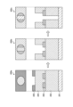
図2は、多層配線の形成の一例を示す図である。図2の状態200aに示すように、多層配線を形成する基板W上には、下地パターン201、層間絶縁膜202、トレンチ用マスク203、ビア用マスク204及びレジスト膜205が積層されている。なお、図2では基板Wは省略している。また、以下の説明では、層間絶縁膜202(被エッチング膜)への積層順に、第1のマスク、第2のマスクと表現する場合がある。図2の場合、層間絶縁膜202が被エッチング膜、トレンチ用マスク203が第1のマスク、ビア用マスク204が第2のマスクとなる。
[Formation of multilayer wiring]
FIG. 2 is a diagram showing an example of formation of multilayer wiring. As shown in the
多層配線の工程では、状態200aから、まずビア用マスク204をエッチングして状態200bとする。次に、状態200bから、層間絶縁膜202をエッチングして状態200cとする。ここで、層間絶縁膜202のエッチングでは、異なる階層に設置された2種類のマスク、つまりトレンチ用マスク203とビア用マスク204とのエッチング選択比が求められる。本実施形態では、このようなエッチング選択比を実現するために、ビア用マスク204(第2のマスク)の側壁に堆積物(以下、サイドデポともいう。)を形成する。
In the multilayer wiring process, the via
図3は、本実施形態におけるプロセスフローの一例を模式的に説明する図である。図3に示すように、状態210では、基板Wに下地パターン221、第1の被エッチング膜222、第2の被エッチング膜223、第1のマスク224、第2のマスク225、SiARC膜226及びレジスト膜227が積層されている。なお、図3では、基板Wは省略している。第1の被エッチング膜222から第2のマスク225について例示すると、第1の被エッチング膜222及び第2の被エッチング膜223は、例えば、SiOC膜又はSiOCH膜などのLow-k膜、SiO2膜が挙げられる。第1のマスク224は、例えば、TiN膜、WC膜等の金属含有膜が挙げられる。第2のマスク225は、例えば、炭素含有膜の一例であるSOC(Spin On Carbon)膜が挙げられる。
FIG. 3 is a diagram schematically explaining an example of the process flow in this embodiment. As shown in FIG. 3, in the
プロセスフローとしては、まず、状態210において、CF4ガス等から生成したプラズマにてSiARC膜226をエッチングして状態211となる。次に、状態211において、N2/H2ガス等から生成したプラズマにて第2のマスク225及びレジスト膜227をエッチングして状態212となる。このとき、第2の被エッチング膜223及び第1のマスク224の一部が露出する。続いて、状態212において、CF4/CHF3ガス等から生成したプラズマにて、露出した第2の被エッチング膜223及びSiARC膜226をエッチングして状態213となる。次に、状態213において、第1のガスから生成したプラズマにて、第2のマスク225の側壁にサイドデポ228を形成して状態214となる。第1のガスは、例えば、炭化水素及び窒素含有ガスであり、C3H6/N2ガス又はCH4/N2等を用いることができる。第1のガスは、炭化水素ガス及び窒素含有ガスとともに、又は窒素含有ガスに代えて、O2、CO等の酸素含有ガスを用いることもできる。また、第1のガスとして、SiH4/CF4、SiF4等のシリコン及びフッ素含有ガスを用いてもよい。続いて、状態214において、第2のガスから生成したプラズマにて、第1の被エッチング膜222をエッチングして状態215となる。第2のガスは、フッ素及び水素含有ガスであり、例えば、CF4/H2ガス、HF/CH4を用いることができる。これにより、第1のマスク224及び第2のマスク225のマスクロスを抑制することができる。
As for the process flow, first, in
[基板処理方法]
次に、本実施形態に係る基板処理方法について説明する。図4は、本実施形態におけるエッチング処理の一例を示すフローチャートである。なお、図4のフローチャートは、図3のプロセスフローのうち、状態213から状態215の処理を詳細に説明したものである。
[Substrate processing method]
Next, a substrate processing method according to this embodiment will be described. FIG. 4 is a flowchart showing an example of etching processing in this embodiment. Note that the flowchart in FIG. 4 describes in detail the processing from
本実施形態に係る基板処理方法では、制御部1bは、図示しない開口部を開放し、プラズマ処理チャンバ10内に、被エッチング膜(層間絶縁膜)がエッチング可能な状態(図3の状態213)の基板Wが搬入され、支持部11(載置台)の静電チャック112に載置される。基板Wは、静電チャック112に直流電圧が印加されることで静電チャック112に保持される。制御部1bは、その後、開口部を閉鎖して排気システム40を制御することにより、プラズマ処理空間10sの雰囲気が所定の真空度になるように、プラズマ処理空間10sから気体を排気する。また、制御部1bは、図示しない温調モジュールを制御することにより、基板Wの温度が所定の温度範囲に含まれるように、温度調整される(ステップS1)。
In the substrate processing method according to the present embodiment, the
次に、制御部1bは、第1のガスとして、C3H6/N2ガスをガス入口12aに供給する。第1のガスは、ガス入口12aに供給された後に、ガス拡散室12bに供給され拡散される。第1のガスは、ガス拡散室12bで拡散された後に、複数のガス出口12cを介して、プラズマ処理チャンバ10のプラズマ処理空間10sにシャワー状に供給され、プラズマ処理空間10sに充填される。
Next, the
制御部1bは、RF電力供給部30を制御することにより、プラズマ励起用のRF信号を下部電極111に供給する。つまり、高周波電力であるRF信号を下部印加する。プラズマ処理空間10sには、下部電極111にRF信号が供給されることにより、プラズマが発生する。このとき、プラズマに自己バイアスがかかることで、逆異方性CVD(Chemical Vapor Deposition)となり、基板Wの第2のマスク225の側壁に堆積物(サイドデポ228)を形成する(ステップS2)。
The
ここで、図5を用いてサイドデポの形成について説明する。図5は、本実施形態におけるサイドデポの形成の一例を模式的に説明する図である。なお、図5では、第1のマスク(図3の第1のマスク224に相当。)は省略している。図5の状態230aでは、下部電極111にRF信号が供給されること(下部印加)により発生するC3H6ガスのプラズマにて、被エッチング膜231(図3の第1の被エッチング膜222に相当。)の上にデポ234が形成される。また、状態230aでは、マスク232(図3の第2のマスク225に相当。)の上にデポ233が形成される。デポ233,234は、イオン起因の異方的供給と、プラズマCVDの等方的重合により形成される。特に、デポ233は、下部印加により、マスク232の側壁に裾が伸びたようなデポが形成される。
Here, the formation of side deposits will be described with reference to FIG. FIG. 5 is a diagram schematically illustrating an example of formation of side deposits in this embodiment. 5, the first mask (corresponding to the
また、図5の状態230bでは、下部印加により発生するN2ガスのプラズマにて、デポ233,234がエッチングされる。Nイオンによる異方性除去により、マスク232の上面のデポ233aは除去されるが、マスク232の側壁のサイドデポ233bは除去されない。デポ234は、Nイオンによる異方性除去により除去される。
Further, in the
このように、ステップS2では、C3H6等の成膜成分を有するガスと、N2等の除去成分を有するガスとを同時に供給してプラズマを生成した場合、デポの形成とデポの除去とが同時に進行する。つまり、状態230aと状態230bとが同時に進行する。この結果、状態230cに示すように、マスク232の側壁にサイドデポ233b(図3のサイドデポ228に相当。)が形成された状態となる。すなわち、サイドデポ233bは、プラズマCVDの本質的な等方性成膜と、RF信号の下部印加によるイオンの異方性供給と、Nによるカーボンの異方的除去とが複合することにより実現することができる。なお、ステップS2は、状態230cに示すようなサイドデポ233bを形成することができる限り、他の方法を採り得る。例えば、成膜成分を有するガスからプラズマを生成してデポを形成する工程と、除去成分を有するガスからプラズマを生成してデポを除去する工程とを逐次的に行うことによりマスク232の側壁にサイドデポ233bを形成してもよい。また、デポを形成する工程とデポを除去する工程とを繰り返すことにより、マスク232の側壁にサイドデポ233bを形成してもよい。
As described above, in step S2, when plasma is generated by simultaneously supplying a gas having a film formation component such as C3H6 and a gas having a removal component such as N2, formation of the deposit and removal of the deposit proceed simultaneously. do. That is,
図4の説明に戻る。制御部1bは、第1のガスが排気されると、第2のガスとして、CF4/H2ガスをガス入口12aに供給する。第2のガスは、ガス入口12aに供給された後に、ガス拡散室12bに供給され拡散される。第2のガスは、ガス拡散室12bで拡散された後に、複数のガス出口12cを介して、プラズマ処理チャンバ10のプラズマ処理空間10sにシャワー状に供給され、プラズマ処理空間10sに充填される。
Returning to the description of FIG. When the first gas is exhausted, the
制御部1bは、RF電力供給部30を制御することにより、プラズマ励起用のRF信号を下部電極111に供給する。つまり、RF信号を下部印加する。プラズマ処理空間10sには、下部電極111にRF信号が供給されることにより、プラズマが発生する。プラズマ処理空間10sでは、基板Wの第1の被エッチング膜222が第2のガスのプラズマによりエッチングされる(ステップS3)。
The
ここで、図6を用いてサイドデポとエッチングの繰り返しについて説明する。図6は、本実施形態におけるサイドデポとエッチングの繰り返しの一例を模式的に説明する図である。なお、図6では、基板W、下地パターン221及び第2の被エッチング膜223は省略している。図6の状態241は、図3の状態213に対応し、第2のマスク225の側壁にサイドデポ228が形成される。図6の状態242では、CF4/H2ガスから生成したプラズマにて、第1の被エッチング膜222がエッチングされる。このとき、イオン244は、第1の被エッチング膜222をエッチングしてトレンチ245を形成する。一方、イオン244は、サイドデポ228が存在することにより、第1のマスク224には衝突せず、第1のマスク224はエッチングされない。状態242では、エッチングによってサイドデポ228が消耗すると、再度、状態241のサイドデポ228の形成に移る。つまり、トレンチ245が所望の深さとなる状態243まで、状態241のサイドデポ228の形成と、状態242の第1の被エッチング膜222のエッチングとを繰り返す。なお、繰り返しの所定回数は、例えば予め実験により求めておくことができる。
Here, repetition of side deposition and etching will be described with reference to FIG. FIG. 6 is a diagram schematically explaining an example of repetition of side deposition and etching in this embodiment. Note that the substrate W, the
図4の説明に戻る。制御部1bは、堆積物の形成工程と、エッチング工程とを所定回数繰り返したか否かを判定する(ステップS4)。所定回数は、例えば3回とすることができる。制御部1bは、所定回数繰り返していないと判定した場合(ステップS4:No)、処理をステップS2に戻す。一方、制御部1bは、所定回数繰り返したと判定した場合(ステップS4:Yes)、処理を終了する。なお、制御部1bは、ステップS4において、被エッチング膜について所定の形状が得られたか否かを判定するようにしてもよい。
Returning to the description of FIG. The
制御部1bは、処理を終了する場合、RF電力供給部30を制御することにより、下部電極111へのRF信号の供給を停止する。また、制御部1bは、静電チャック112へ正負が逆の直流電圧を印加して除電し、基板Wが静電チャック112から剥がされる。制御部1bは、図示しない開口部を開放する。基板Wは、開口部を介してプラズマ処理チャンバ10のプラズマ処理空間10sから搬出される。
When ending the process, the
[実験結果]
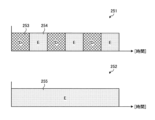
続いて、図7から図11を用いて実験結果について説明する。図7は、本実施形態と比較例とにおけるサイドデポとエッチングの繰り返しを時間軸で表した一例を示す図である。図7のグラフ251に示すように、本実施形態では、下記の処理条件でサイドデポの形成253(「D」)と、エッチング254(「E」)とを3回繰り返した。一方、グラフ252に示すように、比較例では、下記の処理条件でエッチング255(「E」)を1回行った。
[Experimental result]
Next, experimental results will be described with reference to FIGS. 7 to 11. FIG. FIG. 7 is a diagram showing an example of repetition of side deposition and etching in this embodiment and in a comparative example, represented on a time axis. As shown in the
<本実施形態の処理条件>
(サイドデポの形成)
温度 :-70℃
プラズマ処理チャンバ10内の圧力:30mTorr
RF信号の電力 :300W
処理ガス :C3H6/N2=10/290sccm
処理時間 :7秒
(エッチング)
温度 :-70℃
プラズマ処理チャンバ10内の圧力:25mTorr
RF信号の電力 :1400W
処理ガス :CF4/H2=35/130sccm
処理時間 :10秒
<Processing conditions of the present embodiment>
(Formation of side deposit)
Temperature: -70°C
Pressure in plasma processing chamber 10: 30 mTorr
RF signal power: 300W
Processing gas: C3H6/N2=10/290sccm
Processing time: 7 seconds (etching)
Temperature: -70°C
Pressure in plasma processing chamber 10: 25 mTorr
RF signal power: 1400W
Processing gas: CF4/H2=35/130sccm
Processing time: 10 seconds
<比較例の処理条件>
(エッチング)
温度 :-70℃
プラズマ処理チャンバ10内の圧力:25mTorr
RF信号の電力 :1400W
処理ガス :CF4/H2=35/130sccm
処理時間 :10秒,20秒,30秒
<Processing conditions for comparative example>
(etching)
Temperature: -70°C
Pressure in plasma processing chamber 10: 25 mTorr
RF signal power: 1400W
Processing gas: CF4/H2=35/130sccm
Processing time: 10 seconds, 20 seconds, 30 seconds
図8は、本実施形態におけるサイドデポ前後の断面の一例を示す図である。図8に示す断面261は、本実施形態におけるサイドデポの形成前の状態を示す。断面261では、第2の被エッチング膜223、第1のマスク224及び第2のマスク225がエッチングされ、第1の被エッチング膜222がエッチングされる前の状態である。断面262は、本実施形態におけるサイドデポの形成後の状態を示す。断面262では、第2のマスク225の側壁の領域263に、サイドデポ264が形成されていることがわかる。
FIG. 8 is a diagram showing an example of a cross section before and after side deposition in this embodiment. A
図9は、本実施形態における実験結果の一例を示す図である。図9に示す実験結果271~273は、それぞれ上述のステップS2,S3を1回~3回繰り返した場合の結果である。実験結果271~273の中段はCD(Critical Dimension)の値であり、それぞれ33nm、39nm、37nmとなっている。なお、実験結果271~273の下段は、第2のマスク225近傍を拡大したものである。
FIG. 9 is a diagram showing an example of experimental results in this embodiment.
図10は、比較例における実験結果の一例を示す図である。図10に示す実験結果281~283は、比較例の処理条件において処理時間をそれぞれ10秒、20秒、30秒とした場合の結果である。実験結果281~283の中段はCDの値であり、それぞれ39nm、45nm、53nmとなっている。なお、実験結果281~283の下段は、第2のマスク225近傍を拡大したものである。
FIG. 10 is a diagram showing an example of experimental results in a comparative example.
図9の実験結果271~273と、図10の実験結果281~283とを比較すると、実験結果271~273では第1のマスク224(TiN)のロスが発生していないことがわかる。また、CDの値を比較すると、実験結果271~273の方が、Bowingが抑制されていることがわかる。また、実験結果271と実験結果281とを比較すると、エッチングの反応初期においても既にCDの違いが発生していることがわかる。
Comparing the
図11は、サイドデポの有無におけるBowingの比較の一例を示す図である。図11に示す実験結果271aは、図9の実験結果271を拡大したものである。また、図11に示す実験結果281aは、図10の実験結果281を拡大したものである。実験結果271aでは、サイドデポ275が確認でき、CDは33nmとなっている。一方、実験結果281aでは、第2のマスク225の側壁である領域285にサイドデポがなく、CDは39nmとなっている。このことから、CDの広がりであるBowは、第1のマスク224(TiN)のロスだけでなく、イオンの斜め入射によっても起こることが示唆される。すなわち、サイドデポの形成は、第1のマスク224を保護してCDの広がりを抑制できることと、パターンの間口を狭め、垂直入射成分のみを取り込んでBowingを抑制できることとの2つの効果がある。
FIG. 11 is a diagram showing an example of comparison of Bowing with and without side deposit. An
なお、上記した実施形態では、プラズマ処理システム1は、プラズマ処理装置1a及び制御部1bを含む形態としたが、プラズマ処理装置1aと制御部1bとを含む形態で基板処理装置としてもよい。
Although the
以上、本実施形態によれば、基板処理装置(プラズマ処理システム1)は、載置台(支持部11)と、制御部1bとを有する。載置台は、第1の被エッチング膜222と、第1の被エッチング膜222の上に形成された第1のマスク224と、第1のマスク224の少なくとも一部を覆うように形成された第2のマスク225を有する基板Wを載置する。制御部1bは、第1のガスから生成したプラズマにより、第2のマスク225の側壁に保護膜(サイドデポ228)を形成する工程と、第2のガスから生成したプラズマにより、第1の被エッチング膜222をエッチングする工程とを実行する。その結果、積層されたマスクにおけるマスクロスを抑制できる。また、Bowingを抑制できる。
As described above, according to the present embodiment, the substrate processing apparatus (plasma processing system 1) has the mounting table (supporting portion 11) and the
また、本実施形態によれば、形成する工程は、第2のマスク225の上面及び側壁と、第1の被エッチング膜222の表面に堆積物を形成する工程と、第1の被エッチング膜222の表面に形成された堆積物を除去して、第2のマスク225の側壁に保護膜を形成する工程と、を含む。その結果、第1のマスク224を保護することができる。
In addition, according to the present embodiment, the steps of forming include a step of forming deposits on the upper surface and sidewalls of the
また、本実施形態によれば、基板Wが載置される載置台側からRF電力を供給することで第1のガスから生成したプラズマにより、保護膜を形成する。その結果、第2のマスク225の側壁に保護膜を形成できる。
Further, according to the present embodiment, the protective film is formed by plasma generated from the first gas by supplying RF power from the mounting table on which the substrate W is mounted. As a result, a protective film can be formed on the sidewalls of the
また、本実施形態によれば、第2のマスク225で覆われていない第1のマスク224の上部において、第1のマスク224の側壁の位置まで保護膜を形成する。その結果、第1のマスク224を保護することができる。
Further, according to the present embodiment, the protective film is formed up to the side walls of the
また、本実施形態によれば、第1の被エッチング膜222は、Low-k膜又はSiO2膜である。その結果、Bowingを抑制しつつエッチングすることができる。 Further, according to this embodiment, the first film to be etched 222 is a Low-k film or an SiO2 film. As a result, etching can be performed while suppressing bowing.
また、本実施形態によれば、第1のマスク224は、金属含有膜であり、第2のマスク225は、炭素含有膜である。その結果、積層されたマスクにおけるマスクロスを抑制できる。
Also, according to this embodiment, the
また、本実施形態によれば、第1のガスは、炭化水素及び窒素含有ガス、炭化水素及び酸素含有ガス、又は、シリコン及びフッ素含有ガスである。その結果、炭素又はシリコンを含有する保護膜を第2のマスク225の側壁に形成することができる。
Also according to this embodiment, the first gas is a hydrocarbon and nitrogen containing gas, a hydrocarbon and oxygen containing gas, or a silicon and fluorine containing gas. As a result, a protective film containing carbon or silicon can be formed on the sidewalls of the
また、本実施形態によれば、第2のガスは、フッ素及び水素含有ガスである。その結果、第1の被エッチング膜222をエッチングできる。 Also, according to this embodiment, the second gas is a fluorine- and hydrogen-containing gas. As a result, the first film to be etched 222 can be etched.
また、本実施形態によれば、形成する工程及びエッチングする工程は、少なくとも1回以上交互に繰り返される。その結果、積層されたマスクにおけるマスクロスをより抑制できる。 Further, according to this embodiment, the forming step and the etching step are alternately repeated at least once. As a result, mask loss in the stacked masks can be further suppressed.
また、本実施形態によれば、形成する工程及びエッチングする工程は、同一の処理容器内で行われる。その結果、形成する工程及びエッチングする工程の繰り返しを効率よく行うことができる。 Further, according to this embodiment, the forming step and the etching step are performed in the same processing container. As a result, it is possible to efficiently repeat the forming step and the etching step.
また、本実施形態によれば、形成する工程及びエッチングする工程は、異なる処理容器内で行われる。その結果、複数の基板Wに対して処理を行う場合に、それぞれの工程を効率よく行うことができる。 Further, according to this embodiment, the forming step and the etching step are performed in different processing vessels. As a result, when processing a plurality of substrates W, each process can be performed efficiently.
以上、種々の例示的実施形態について説明してきたが、上述した例示的実施形態に限定されることなく、様々な追加、省略、置換、及び変更がなされてもよい。また、異なる実施形態における要素を組み合わせて他の実施形態を形成することが可能である。 While various exemplary embodiments have been described above, various additions, omissions, substitutions, and modifications may be made without being limited to the exemplary embodiments described above. Also, elements from different embodiments can be combined to form other embodiments.
例えば、上述した実施形態では、被エッチング膜の上に形成された第1のマスクと、第1のマスクの少なくとも一部を覆うように形成された第2のマスクとを含む2段マスクが設けられた基板Wを処理対象とした。しかし、このような2段マスクを有する基板に限らず、多段マスクを有する基板を対象とすることもできる。ここで、多段マスクを有する基板とは、被エッチング膜と、当該被エッチング膜の上に、被エッチング膜から第n段目の第nのマスクと(nは1以上の整数)、被エッチング膜から第(n+1)段目のマスクであり、第nのマスクの少なくとも一部覆うように形成された第(n+1)のマスクとを備える多段マスクと、を有する基板を意味する。 For example, in the above-described embodiments, a two-stage mask including a first mask formed on the film to be etched and a second mask formed to cover at least part of the first mask is provided. The substrate W thus obtained was used as a processing target. However, the present invention is not limited to substrates having such two-stage masks, and substrates having multi-stage masks can also be used. Here, a substrate having a multi-stage mask means a film to be etched, an n-th mask (n is an integer of 1 or more) on the film to be etched, and an n-th mask (n is an integer of 1 or more) on the film to be etched. and (n+1)-th mask formed to at least partially cover the n-th mask.
多段マスクを有する基板に対しても、上述した実施形態と同様に処理することができる。具体的には、多段マスクを有する基板をプラズマ処理チャンバ10内に搬入し、載置台(支持部11)上に設けられた静電チャック112上に保持する。続いて、第1のガスから生成したプラズマにより、被エッチング膜の上に形成された第1のマスク以外のいずれか1以上のマスクの側壁に保護膜が形成する。その後、第2のガスから生成したプラズマにより、被エッチング膜をエッチングする。
A substrate having a multi-stage mask can also be processed in the same manner as in the above-described embodiments. Specifically, a substrate having a multistage mask is carried into the
なお、多段マスクを有する基板を対象とする場合も、上述した実施形態と同様に、第1のマスク以外のいずれか1以上のマスクの側壁と、被エッチング膜の表面に堆積物を形成した後、被エッチング膜の表面に形成された堆積物を除去することにより保護膜を形成してもよい。また、基板が載置される載置台側からRF電力を供給することで第1のガスから生成したプラズマにより保護膜を形成してもよい。また、保護膜は、第1のマスクの上部において、第1のマスクの側壁の位置まで形成してもよい。 In the case of a substrate having a multistage mask, as in the above-described embodiments, after deposits are formed on the sidewalls of any one or more masks other than the first mask and on the surface of the film to be etched, Alternatively, the protective film may be formed by removing deposits formed on the surface of the film to be etched. Alternatively, the protection film may be formed by plasma generated from the first gas by supplying RF power from the mounting table on which the substrate is mounted. Also, the protective film may be formed on the upper portion of the first mask up to the position of the sidewall of the first mask.
なお、他の手法として、不飽和ALD(Atomic Layer Deposition)を用いてトレンチの途中まで成膜することが考えられる。ところが、不飽和ALDは、アスペクト比が高い(例えば5以上。)のものが対象であり、アスペクト比の低い多層配線形成用パターンに適用しようとすると、トレンチの底まで成膜されてしまう。また、トレンチの底の膜を取り除こうとすると、マスク上に成膜された膜まで剥がれてしまう。これに対し、上述の本実施形態では、アスペクト比の低い多層配線形成用パターンであっても、トレンチの底には成膜せず、サイドデポを形成することができるので、十分な選択比を取ることができ、被エッチング膜を選択的にエッチングすることができる。 As another method, it is conceivable to use unsaturated ALD (Atomic Layer Deposition) to form a film up to the middle of the trench. However, unsaturated ALD is intended for those with a high aspect ratio (for example, 5 or more), and if it is applied to a multilayer wiring pattern with a low aspect ratio, the film is formed to the bottom of the trench. In addition, if the film on the bottom of the trench is removed, the film formed on the mask is also peeled off. On the other hand, in the present embodiment described above, even if the pattern for forming a multilayer wiring has a low aspect ratio, it is possible to form a side deposit without forming a film on the bottom of the trench. It is possible to selectively etch the film to be etched.
また、上記した実施形態では、第1のガスとして、炭化水素及び窒素含有ガスを用いたが、これに限定されない。例えば、被エッチング膜やマスクの材質に応じて、ケイ素及びフッ素含有ガスや、金属元素(Ti,W)及び塩素含有ガスを用いてもよい。 Further, in the above-described embodiment, a hydrocarbon and a nitrogen-containing gas are used as the first gas, but the present invention is not limited to this. For example, a gas containing silicon and fluorine or a gas containing metal elements (Ti, W) and chlorine may be used depending on the material of the film to be etched and the mask.
また、上記した実施形態では、RF信号を下部印加したが、バイアス成分が入っていれば、上部印加の基板処理装置を用いてもよい。なお、バイアスを調整することで、サイドデポの形成位置を調整することができる。 In the above-described embodiment, the RF signal is applied from the bottom, but a substrate processing apparatus that applies the RF signal from the top may be used as long as it contains a bias component. By adjusting the bias, the formation position of the side deposit can be adjusted.
1 プラズマ処理システム
1a プラズマ処理装置
1b 制御部
10 プラズマ処理チャンバ
11 支持部
20 ガス供給部
30 RF電力供給部
40 排気システム
222 第1の被エッチング膜
224 第1のマスク
225 第2のマスク
228 サイドデポ(堆積物)
W 基板
1
W substrate
Claims (18)
第1のガスから生成したプラズマにより、前記第2のマスクの側壁に保護膜を形成する工程と、
第2のガスから生成したプラズマにより、前記被エッチング膜をエッチングする工程と、
を有する基板処理方法。 a film to be etched; a first mask on the film to be etched , the first mask having an opening with a first opening width ; and a second mask covering a part of the first mask. providing a substrate including a second mask having an opening with a second opening width greater than the first opening width ;
forming a protective film on sidewalls of the second mask by plasma generated from a first gas;
etching the film to be etched with plasma generated from a second gas;
A substrate processing method comprising:
前記第2のマスクの上面及び側壁と、前記被エッチング膜の表面に堆積物を形成する工程と、
前記被エッチング膜の表面に形成された前記堆積物を除去する工程と、を含む、
請求項1に記載の基板処理方法。 The step of forming the protective film includes
forming a deposit on the top surface and sidewalls of the second mask and on the surface of the film to be etched;
and removing the deposit formed on the surface of the film to be etched.
The substrate processing method according to claim 1.
請求項1又は2に記載の基板処理方法。 The step of forming the protective film includes forming the protective film by plasma generated from the first gas by supplying RF power to a mounting table on which the substrate is mounted.
The substrate processing method according to claim 1 or 2.
請求項1~3のいずれか1つに記載の基板処理方法。 In the step of forming the protective film , the protective film is formed up to the position of the sidewall of the first mask in the upper part of the first mask not covered with the second mask.
The substrate processing method according to any one of claims 1 to 3.
請求項1~4のいずれか1つに記載の基板処理方法。 The film to be etched is a Low-k film or a SiO film,
The substrate processing method according to any one of claims 1 to 4.
請求項1~5のいずれか1つに記載の基板処理方法。 wherein the first mask is a metal-containing film and the second mask is a carbon-containing film;
The substrate processing method according to any one of claims 1 to 5.
請求項1~6のいずれか1つに記載の基板処理方法。 wherein the first gas is a hydrocarbon and nitrogen containing gas, a hydrocarbon and oxygen containing gas, or a silicon and fluorine containing gas;
The substrate processing method according to any one of claims 1 to 6.
請求項1~7のいずれか1つに記載の基板処理方法。 wherein the second gas is a fluorine and hydrogen containing gas;
The substrate processing method according to any one of claims 1 to 7.
請求項1~8のいずれか1つに記載の基板処理方法。 The step of forming the protective film and the step of etching the film to be etched are alternately repeated at least one time.
The substrate processing method according to any one of claims 1 to 8.
請求項1~9のいずれか1つに記載の基板処理方法。 The step of forming the protective film and the step of etching the film to be etched are performed in the same processing container,
The substrate processing method according to any one of claims 1 to 9.
請求項1~9のいずれか1つに記載の基板処理方法。 The step of forming the protective film and the step of etching the film to be etched are performed in different processing containers,
The substrate processing method according to any one of claims 1 to 9.
前記被エッチング膜と、前記第1のマスクと、前記第1のマスクを覆う第2のマスクと、前記第2のマスク上の第3のマスクであって前記第2開口幅の開口部を有する第3のマスクとを含む基板を提供する工程と、The film to be etched, the first mask, a second mask covering the first mask, and a third mask on the second mask having an opening with the second opening width. providing a substrate including a third mask;
前記被エッチング膜を露出するために前記第3のマスクを通して前記第2のマスクをエッチングする工程と、をさらに備える、etching the second mask through the third mask to expose the film to be etched;
請求項1に記載の基板処理方法。The substrate processing method according to claim 1.
請求項2に記載の基板処理方法。The substrate processing method according to claim 2.
請求項2に記載の基板処理方法。The substrate processing method according to claim 2.
請求項2に記載の基板処理方法。The substrate processing method according to claim 2.
請求項1~15のいずれか1つに記載の基板処理方法。The substrate processing method according to any one of claims 1 to 15.
第1のガスから生成したプラズマにより、前記多段マスクのうち第1のマスク以外のいずれか1以上のマスクの側壁に保護膜を形成する工程と、
第2のガスから生成したプラズマにより、前記被エッチング膜をエッチングする工程と、
を有する基板処理方法。 A step of providing a substrate including a film to be etched and a multi-stage mask formed on the film to be etched, wherein the multi-stage mask is an n-th mask at an n-th stage from the film to be etched. an n-th mask having an opening with an n-th opening width (n is an integer equal to or greater than 1), and a portion of the n-th mask, which is the (n+1)-th mask from the film to be etched. a (n+1)-th mask covering the above, the (n+1)-th mask having an opening with an (n+1)-th opening width larger than the n-th opening width;
forming a protective film on sidewalls of at least one of the multi-stage masks other than the first mask by plasma generated from a first gas;
etching the film to be etched with plasma generated from a second gas;
A substrate processing method comprising:
第1のガスから生成したプラズマにより、前記第2のマスクの側壁に保護膜を形成する工程と、第2のガスから生成したプラズマにより、前記被エッチング膜をエッチングする工程とを実行する制御部と、
を有する基板処理装置。 a film to be etched; a first mask on the film to be etched , the first mask having an opening with a first opening width ; and a second mask covering a part of the first mask. a mounting table for mounting a substrate including a second mask having an opening with a second opening width larger than the first opening width ;
A control unit for forming a protective film on the sidewall of the second mask with plasma generated from a first gas and etching the film to be etched with plasma generated from a second gas. and,
A substrate processing apparatus having
Priority Applications (5)
| Application Number | Priority Date | Filing Date | Title |
|---|---|---|---|
| JP2019233668A JP7333752B2 (en) | 2019-12-25 | 2019-12-25 | Substrate processing method and substrate processing apparatus |
| TW109143749A TW202129756A (en) | 2019-12-25 | 2020-12-11 | Substrate processing method and substrate processing apparatus |
| CN202011472515.3A CN113035708A (en) | 2019-12-25 | 2020-12-15 | Substrate processing method and substrate processing apparatus |
| KR1020200183198A KR20210082384A (en) | 2019-12-25 | 2020-12-24 | Substrate processing method and substrate processing apparatus |
| US17/133,974 US11501975B2 (en) | 2019-12-25 | 2020-12-24 | Substrate processing method and substrate processing apparatus |
Applications Claiming Priority (1)
| Application Number | Priority Date | Filing Date | Title |
|---|---|---|---|
| JP2019233668A JP7333752B2 (en) | 2019-12-25 | 2019-12-25 | Substrate processing method and substrate processing apparatus |
Publications (3)
| Publication Number | Publication Date |
|---|---|
| JP2021103710A JP2021103710A (en) | 2021-07-15 |
| JP2021103710A5 JP2021103710A5 (en) | 2022-10-21 |
| JP7333752B2 true JP7333752B2 (en) | 2023-08-25 |
Family
ID=76459255
Family Applications (1)
| Application Number | Title | Priority Date | Filing Date |
|---|---|---|---|
| JP2019233668A Active JP7333752B2 (en) | 2019-12-25 | 2019-12-25 | Substrate processing method and substrate processing apparatus |
Country Status (5)
| Country | Link |
|---|---|
| US (1) | US11501975B2 (en) |
| JP (1) | JP7333752B2 (en) |
| KR (1) | KR20210082384A (en) |
| CN (1) | CN113035708A (en) |
| TW (1) | TW202129756A (en) |
Families Citing this family (2)
| Publication number | Priority date | Publication date | Assignee | Title |
|---|---|---|---|---|
| WO2024024919A1 (en) * | 2022-07-29 | 2024-02-01 | 東京エレクトロン株式会社 | Substrate processing method and substrate processing system |
| KR20240128194A (en) * | 2023-02-17 | 2024-08-26 | 피에스케이 주식회사 | Substrate processing method and apparatus |
Citations (12)
| Publication number | Priority date | Publication date | Assignee | Title |
|---|---|---|---|---|
| JP2006032908A (en) | 2004-06-16 | 2006-02-02 | Tokyo Electron Ltd | Manufacturing method of semiconductor device |
| JP2007005377A (en) | 2005-06-21 | 2007-01-11 | Tokyo Electron Ltd | Plasma etching method, control program, computer storage medium and plasma etching apparatus |
| JP2009044090A (en) | 2007-08-10 | 2009-02-26 | Tokyo Electron Ltd | Method of manufacturing semiconductor apparatus, and storage medium |
| WO2009154173A1 (en) | 2008-06-17 | 2009-12-23 | 株式会社アルバック | Method for manufacturing multistep substrate |
| JP2010135624A (en) | 2008-12-05 | 2010-06-17 | Tokyo Electron Ltd | Method of manufacturing semiconductor device |
| JP2010514224A5 (en) | 2007-12-18 | 2011-02-03 | ||
| JP2013021192A (en) | 2011-07-12 | 2013-01-31 | Tokyo Electron Ltd | Plasma etching method |
| JP2013077594A (en) | 2011-09-29 | 2013-04-25 | Tokyo Electron Ltd | Plasma etching method and method of manufacturing semiconductor device |
| JP2013258244A (en) | 2012-06-12 | 2013-12-26 | Tokyo Electron Ltd | Etching method and plasma processing apparatus |
| JP2015170763A (en) | 2014-03-07 | 2015-09-28 | ルネサスエレクトロニクス株式会社 | Semiconductor device manufacturing method |
| JP2016115719A (en) | 2014-12-11 | 2016-06-23 | 東京エレクトロン株式会社 | Plasma etching method |
| JP2017143194A (en) | 2016-02-10 | 2017-08-17 | Sppテクノロジーズ株式会社 | Semiconductor element manufacturing method |
Family Cites Families (10)
| Publication number | Priority date | Publication date | Assignee | Title |
|---|---|---|---|---|
| JPH01194325A (en) * | 1988-01-29 | 1989-08-04 | Toshiba Corp | Dry-etching |
| US6569774B1 (en) * | 2000-08-31 | 2003-05-27 | Micron Technology, Inc. | Method to eliminate striations and surface roughness caused by dry etch |
| KR100606540B1 (en) * | 2004-12-22 | 2006-08-01 | 동부일렉트로닉스 주식회사 | Method for forming the copper interconnection of semiconductor device |
| US7902078B2 (en) * | 2006-02-17 | 2011-03-08 | Tokyo Electron Limited | Processing method and plasma etching method |
| US7786019B2 (en) | 2006-12-18 | 2010-08-31 | Applied Materials, Inc. | Multi-step photomask etching with chlorine for uniformity control |
| US8476168B2 (en) * | 2011-01-26 | 2013-07-02 | International Business Machines Corporation | Non-conformal hardmask deposition for through silicon etch |
| US20150079760A1 (en) * | 2013-09-19 | 2015-03-19 | Wei-Sheng Lei | Alternating masking and laser scribing approach for wafer dicing using laser scribing and plasma etch |
| JP6836953B2 (en) | 2016-12-13 | 2021-03-03 | 東京エレクトロン株式会社 | A method of selectively etching a first region formed of silicon nitride with respect to a second region formed of silicon oxide. |
| US20220076962A1 (en) * | 2019-02-27 | 2022-03-10 | Lam Research Corporation | Semiconductor mask reshaping using a sacrificial layer |
| CN112151608B (en) * | 2019-06-28 | 2023-12-15 | 中芯国际集成电路制造(上海)有限公司 | Semiconductor structure and forming method thereof |
-
2019
- 2019-12-25 JP JP2019233668A patent/JP7333752B2/en active Active
-
2020
- 2020-12-11 TW TW109143749A patent/TW202129756A/en unknown
- 2020-12-15 CN CN202011472515.3A patent/CN113035708A/en active Pending
- 2020-12-24 US US17/133,974 patent/US11501975B2/en active Active
- 2020-12-24 KR KR1020200183198A patent/KR20210082384A/en active Search and Examination
Patent Citations (12)
| Publication number | Priority date | Publication date | Assignee | Title |
|---|---|---|---|---|
| JP2006032908A (en) | 2004-06-16 | 2006-02-02 | Tokyo Electron Ltd | Manufacturing method of semiconductor device |
| JP2007005377A (en) | 2005-06-21 | 2007-01-11 | Tokyo Electron Ltd | Plasma etching method, control program, computer storage medium and plasma etching apparatus |
| JP2009044090A (en) | 2007-08-10 | 2009-02-26 | Tokyo Electron Ltd | Method of manufacturing semiconductor apparatus, and storage medium |
| JP2010514224A5 (en) | 2007-12-18 | 2011-02-03 | ||
| WO2009154173A1 (en) | 2008-06-17 | 2009-12-23 | 株式会社アルバック | Method for manufacturing multistep substrate |
| JP2010135624A (en) | 2008-12-05 | 2010-06-17 | Tokyo Electron Ltd | Method of manufacturing semiconductor device |
| JP2013021192A (en) | 2011-07-12 | 2013-01-31 | Tokyo Electron Ltd | Plasma etching method |
| JP2013077594A (en) | 2011-09-29 | 2013-04-25 | Tokyo Electron Ltd | Plasma etching method and method of manufacturing semiconductor device |
| JP2013258244A (en) | 2012-06-12 | 2013-12-26 | Tokyo Electron Ltd | Etching method and plasma processing apparatus |
| JP2015170763A (en) | 2014-03-07 | 2015-09-28 | ルネサスエレクトロニクス株式会社 | Semiconductor device manufacturing method |
| JP2016115719A (en) | 2014-12-11 | 2016-06-23 | 東京エレクトロン株式会社 | Plasma etching method |
| JP2017143194A (en) | 2016-02-10 | 2017-08-17 | Sppテクノロジーズ株式会社 | Semiconductor element manufacturing method |
Also Published As
| Publication number | Publication date |
|---|---|
| US20210202262A1 (en) | 2021-07-01 |
| US11501975B2 (en) | 2022-11-15 |
| TW202129756A (en) | 2021-08-01 |
| CN113035708A (en) | 2021-06-25 |
| KR20210082384A (en) | 2021-07-05 |
| JP2021103710A (en) | 2021-07-15 |
Similar Documents
| Publication | Publication Date | Title |
|---|---|---|
| KR101029947B1 (en) | A method for plasma etching performance enhancement | |
| KR20190037341A (en) | A fabrication method for protecting ULK material from damage during etching processing to obtain a desired feature | |
| KR101075045B1 (en) | A method for plasma etching performance enhancement | |
| JP2008198659A (en) | Plasma etching method | |
| JP7333752B2 (en) | Substrate processing method and substrate processing apparatus | |
| US11121002B2 (en) | Systems and methods for etching metals and metal derivatives | |
| KR20220154787A (en) | Systems and methods for aluminum containing film removal | |
| KR20170058863A (en) | Plasma etching method | |
| KR20110030295A (en) | Mask pattern forming method and semiconductor device manufacturing method | |
| KR102581284B1 (en) | Systems and methods to form airgaps | |
| WO2022244678A1 (en) | Substrate processing method and substrate processing apparatus | |
| JP7483933B2 (en) | Systems and methods for nitride-containing film removal - Patents.com | |
| KR20220136136A (en) | Etching method and etching processing apparatus | |
| TW202213459A (en) | Methods for etching structures with oxygen pulsing | |
| US10438774B2 (en) | Etching method and plasma processing apparatus | |
| JP2007059666A (en) | Manufacturing method and apparatus for semiconductor device, control program, and computer memory medium | |
| TW201937593A (en) | Plasma etching method and plasma etching apparatus | |
| WO2024009815A1 (en) | Substrate processing method | |
| JP2019029619A (en) | Method for processing workpiece | |
| US20240258116A1 (en) | Systems and methods for titanium-containing film removal | |
| US20220238348A1 (en) | Substrate processing method and substrate processing apparatus | |
| JP2022179327A (en) | Substrate processing method and substrate processing apparatus | |
| JP2024001464A (en) | Etching method and plasma processing apparatus | |
| JP6169521B2 (en) | Plasma etching method | |
| US20180358227A1 (en) | Method For Reducing Reactive Ion Etch Lag in Low K Dielectric Etching |
Legal Events
| Date | Code | Title | Description |
|---|---|---|---|
| A521 | Request for written amendment filed |
Free format text: JAPANESE INTERMEDIATE CODE: A523 Effective date: 20221012 |
|
| A621 | Written request for application examination |
Free format text: JAPANESE INTERMEDIATE CODE: A621 Effective date: 20221012 |
|
| A977 | Report on retrieval |
Free format text: JAPANESE INTERMEDIATE CODE: A971007 Effective date: 20230706 |
|
| TRDD | Decision of grant or rejection written | ||
| A01 | Written decision to grant a patent or to grant a registration (utility model) |
Free format text: JAPANESE INTERMEDIATE CODE: A01 Effective date: 20230718 |
|
| A61 | First payment of annual fees (during grant procedure) |
Free format text: JAPANESE INTERMEDIATE CODE: A61 Effective date: 20230815 |
|
| R150 | Certificate of patent or registration of utility model |
Ref document number: 7333752 Country of ref document: JP Free format text: JAPANESE INTERMEDIATE CODE: R150 |