JP7311152B2 - Crystal oscillator electrode structure, crystal oscillator, crystal oscillator - Google Patents
Crystal oscillator electrode structure, crystal oscillator, crystal oscillator Download PDFInfo
- Publication number
- JP7311152B2 JP7311152B2 JP2020047607A JP2020047607A JP7311152B2 JP 7311152 B2 JP7311152 B2 JP 7311152B2 JP 2020047607 A JP2020047607 A JP 2020047607A JP 2020047607 A JP2020047607 A JP 2020047607A JP 7311152 B2 JP7311152 B2 JP 7311152B2
- Authority
- JP
- Japan
- Prior art keywords
- electrode
- crystal
- area
- crystal oscillator
- main surface
- Prior art date
- Legal status (The legal status is an assumption and is not a legal conclusion. Google has not performed a legal analysis and makes no representation as to the accuracy of the status listed.)
- Active
Links
- 239000013078 crystal Substances 0.000 title claims description 202
- 230000005284 excitation Effects 0.000 claims description 75
- 239000002184 metal Substances 0.000 claims description 49
- 229910052751 metal Inorganic materials 0.000 claims description 49
- 238000000034 method Methods 0.000 claims description 22
- 239000010953 base metal Substances 0.000 claims description 15
- 238000004519 manufacturing process Methods 0.000 claims description 15
- 230000010355 oscillation Effects 0.000 claims description 5
- 229910052759 nickel Inorganic materials 0.000 claims description 4
- 229910052721 tungsten Inorganic materials 0.000 claims description 4
- 229910052782 aluminium Inorganic materials 0.000 claims description 3
- 229910052709 silver Inorganic materials 0.000 claims description 3
- 229910052804 chromium Inorganic materials 0.000 claims description 2
- 229910052802 copper Inorganic materials 0.000 claims description 2
- 229910052737 gold Inorganic materials 0.000 claims description 2
- 229910052749 magnesium Inorganic materials 0.000 claims description 2
- 239000010410 layer Substances 0.000 description 24
- 238000000605 extraction Methods 0.000 description 14
- 238000006073 displacement reaction Methods 0.000 description 10
- 239000000853 adhesive Substances 0.000 description 8
- 230000001070 adhesive effect Effects 0.000 description 8
- 230000007423 decrease Effects 0.000 description 6
- 238000005530 etching Methods 0.000 description 6
- 238000010586 diagram Methods 0.000 description 4
- 238000004088 simulation Methods 0.000 description 4
- 238000000206 photolithography Methods 0.000 description 3
- 239000002356 single layer Substances 0.000 description 3
- PNEYBMLMFCGWSK-UHFFFAOYSA-N aluminium oxide Inorganic materials [O-2].[O-2].[O-2].[Al+3].[Al+3] PNEYBMLMFCGWSK-UHFFFAOYSA-N 0.000 description 2
- 239000000919 ceramic Substances 0.000 description 2
- 239000012141 concentrate Substances 0.000 description 2
- 230000000694 effects Effects 0.000 description 2
- 238000003754 machining Methods 0.000 description 2
- 239000000523 sample Substances 0.000 description 2
- 238000007740 vapor deposition Methods 0.000 description 2
- 230000008878 coupling Effects 0.000 description 1
- 238000010168 coupling process Methods 0.000 description 1
- 238000005859 coupling reaction Methods 0.000 description 1
- 238000005520 cutting process Methods 0.000 description 1
- 238000005516 engineering process Methods 0.000 description 1
- 238000007306 functionalization reaction Methods 0.000 description 1
- 230000000873 masking effect Effects 0.000 description 1
- 238000005498 polishing Methods 0.000 description 1
- 239000010453 quartz Substances 0.000 description 1
- 230000007261 regionalization Effects 0.000 description 1
- VYPSYNLAJGMNEJ-UHFFFAOYSA-N silicon dioxide Inorganic materials O=[Si]=O VYPSYNLAJGMNEJ-UHFFFAOYSA-N 0.000 description 1
- 230000006641 stabilisation Effects 0.000 description 1
- 238000011105 stabilization Methods 0.000 description 1
- 239000013585 weight reducing agent Substances 0.000 description 1
- 238000001039 wet etching Methods 0.000 description 1
Images


Classifications
-
- H—ELECTRICITY
- H03—ELECTRONIC CIRCUITRY
- H03H—IMPEDANCE NETWORKS, e.g. RESONANT CIRCUITS; RESONATORS
- H03H9/00—Networks comprising electromechanical or electro-acoustic devices; Electromechanical resonators
- H03H9/02—Details
- H03H9/125—Driving means, e.g. electrodes, coils
- H03H9/13—Driving means, e.g. electrodes, coils for networks consisting of piezoelectric or electrostrictive materials
-
- H—ELECTRICITY
- H03—ELECTRONIC CIRCUITRY
- H03H—IMPEDANCE NETWORKS, e.g. RESONANT CIRCUITS; RESONATORS
- H03H9/00—Networks comprising electromechanical or electro-acoustic devices; Electromechanical resonators
- H03H9/02—Details
- H03H9/05—Holders; Supports
- H03H9/10—Mounting in enclosures
- H03H9/1007—Mounting in enclosures for bulk acoustic wave [BAW] devices
- H03H9/1014—Mounting in enclosures for bulk acoustic wave [BAW] devices the enclosure being defined by a frame built on a substrate and a cap, the frame having no mechanical contact with the BAW device
- H03H9/1021—Mounting in enclosures for bulk acoustic wave [BAW] devices the enclosure being defined by a frame built on a substrate and a cap, the frame having no mechanical contact with the BAW device the BAW device being of the cantilever type
-
- H—ELECTRICITY
- H03—ELECTRONIC CIRCUITRY
- H03B—GENERATION OF OSCILLATIONS, DIRECTLY OR BY FREQUENCY-CHANGING, BY CIRCUITS EMPLOYING ACTIVE ELEMENTS WHICH OPERATE IN A NON-SWITCHING MANNER; GENERATION OF NOISE BY SUCH CIRCUITS
- H03B5/00—Generation of oscillations using amplifier with regenerative feedback from output to input
- H03B5/30—Generation of oscillations using amplifier with regenerative feedback from output to input with frequency-determining element being electromechanical resonator
-
- H—ELECTRICITY
- H03—ELECTRONIC CIRCUITRY
- H03H—IMPEDANCE NETWORKS, e.g. RESONANT CIRCUITS; RESONATORS
- H03H9/00—Networks comprising electromechanical or electro-acoustic devices; Electromechanical resonators
- H03H9/02—Details
- H03H9/05—Holders; Supports
- H03H9/0538—Constructional combinations of supports or holders with electromechanical or other electronic elements
- H03H9/0547—Constructional combinations of supports or holders with electromechanical or other electronic elements consisting of a vertical arrangement
-
- H—ELECTRICITY
- H03—ELECTRONIC CIRCUITRY
- H03H—IMPEDANCE NETWORKS, e.g. RESONANT CIRCUITS; RESONATORS
- H03H9/00—Networks comprising electromechanical or electro-acoustic devices; Electromechanical resonators
- H03H9/02—Details
- H03H9/125—Driving means, e.g. electrodes, coils
- H03H9/13—Driving means, e.g. electrodes, coils for networks consisting of piezoelectric or electrostrictive materials
- H03H9/131—Driving means, e.g. electrodes, coils for networks consisting of piezoelectric or electrostrictive materials consisting of a multilayered structure
-
- H—ELECTRICITY
- H03—ELECTRONIC CIRCUITRY
- H03H—IMPEDANCE NETWORKS, e.g. RESONANT CIRCUITS; RESONATORS
- H03H9/00—Networks comprising electromechanical or electro-acoustic devices; Electromechanical resonators
- H03H9/15—Constructional features of resonators consisting of piezoelectric or electrostrictive material
- H03H9/17—Constructional features of resonators consisting of piezoelectric or electrostrictive material having a single resonator
- H03H9/176—Constructional features of resonators consisting of piezoelectric or electrostrictive material having a single resonator consisting of ceramic material
-
- H—ELECTRICITY
- H03—ELECTRONIC CIRCUITRY
- H03H—IMPEDANCE NETWORKS, e.g. RESONANT CIRCUITS; RESONATORS
- H03H9/00—Networks comprising electromechanical or electro-acoustic devices; Electromechanical resonators
- H03H9/15—Constructional features of resonators consisting of piezoelectric or electrostrictive material
- H03H9/17—Constructional features of resonators consisting of piezoelectric or electrostrictive material having a single resonator
- H03H9/19—Constructional features of resonators consisting of piezoelectric or electrostrictive material having a single resonator consisting of quartz
Description
本発明は、水晶振動子の電極構造と、水晶振動子と、水晶発振器と、に関する。 The present invention relates to a crystal oscillator electrode structure, a crystal oscillator, and a crystal oscillator.
近年、水晶振動子を搭載する各種デバイスの小型化・軽量化・多機能化が進み、同デバイスに用いられる水晶振動子には、小型かつ高性能な水晶振動子が求められている。水晶振動子が小型化されると、水晶振動子に用いられる水晶片(ブランク)と、水晶片に配置される励振電極の面積も小さくなる。その結果、水晶振動子(水晶片)の等価直列抵抗(CI:Crystal Impedance)値は、大きくなる。また、主振動がインハーモニックなどの副振動の影響を受け易くなる。そのため、水晶片を筐体に搭載する場合、副振動の影響を抑制するような接着剤の条件(例えば、接着剤の塗布位置や塗布量)は厳しくなり、量産時の歩留の低下などの問題が生じ易くなる。 In recent years, the miniaturization, weight reduction, and multi-functionalization of various devices equipped with crystal oscillators have progressed, and crystal oscillators used in such devices are required to be compact and have high performance. When the crystal oscillator is miniaturized, the areas of the crystal piece (blank) used for the crystal oscillator and the excitation electrodes arranged on the crystal piece are also reduced. As a result, the equivalent series resistance (CI: Crystal Impedance) value of the crystal oscillator (crystal blank) increases. In addition, the primary vibration is likely to be affected by secondary vibration such as inharmonic vibration. Therefore, when the crystal element is mounted on the housing, the adhesive conditions (for example, adhesive application position and application amount) to suppress the influence of the secondary vibration become severe, and there is a problem such as a decrease in yield during mass production. problems are more likely to occur.
これまでにも、水晶片の側面の形状を精密に加工することで、小型化かつ高性能な水晶振動子を製造する技術が提案されている(例えば、特許文献1参照)。 Techniques have been proposed so far for manufacturing a compact and high-performance crystal oscillator by precisely processing the shape of the side surface of the crystal blank (see, for example, Patent Document 1).
特許文献1に開示の技術は、水晶片の各軸方向を調整し、ウェットエッチングにおいて、水晶片の-X軸方向の側面に2つの結晶面を形成し、水晶片の+X軸方向の側面に6つ(または4つ)の結晶面を形成する。その結果、副振動が抑制され、振動片のCI値が低減される。しかしながら、同技術は、所望の結晶面を形成するために、フォトリソ工程におけるマスクパターン形成や水晶片の厚みのエッチング量に数μmオーダーの精密な制御を必要とすると共に、多くの工程を必要とする。そのため、同技術において、各工程間の歩留を低下させることなく、高い生産性を維持することは、極めて困難である。
The technique disclosed in
本発明は、精密な水晶片の加工を要することなくCI値を低減可能な水晶振動子の電極構造と、水晶振動子と、水晶発振器と、を提供することを目的とする。 An object of the present invention is to provide an electrode structure of a crystal oscillator, a crystal oscillator, and a crystal oscillator that can reduce the CI value without requiring precise machining of the crystal piece.
本発明にかかる水晶振動子の電極構造と、水晶振動子と、水晶発振器とは、水晶片の主面上の少なくとも中央に配置される励振電極、を有してなり、励振電極は、水晶片の厚み滑り振動の振動エネルギーを水晶片の中央領域に集中させる構造を有することを特徴とする。 The electrode structure of the crystal oscillator, the crystal oscillator, and the crystal oscillator according to the present invention each have an excitation electrode arranged at least in the center on the main surface of the crystal blank, and the excitation electrode is the crystal blank. It has a structure in which the vibration energy of the thickness-shear vibration is concentrated in the central region of the crystal piece.
本発明によれば、精密な水晶片の加工を要することなくCI値を低減できる。 According to the present invention, the CI value can be reduced without requiring precise machining of the crystal piece.
以下、図面を参照しながら、本発明にかかる水晶振動子の電極構造(以下「本構造」という。)と、水晶振動子と、水晶発振器と、の実施の形態について説明する。各図において、同一の部材については同一の符号を付し、重複する説明は省略する。 DESCRIPTION OF THE PREFERRED EMBODIMENTS Embodiments of a crystal resonator electrode structure (hereinafter referred to as "this structure"), a crystal resonator, and a crystal oscillator according to the present invention will be described below with reference to the drawings. In each figure, the same reference numerals are given to the same members, and overlapping descriptions are omitted.
●水晶振動子●
先ず、本発明にかかる水晶振動子と本構造の実施の形態について説明する。
●Crystal oscillator●
First, an embodiment of a crystal resonator and this structure according to the present invention will be described.
図1(a)は本発明にかかる水晶振動子の実施の形態を示す模式平面図であり、(b)は(a)の水晶振動子のAA線における模式断面図である。同図は、説明の便宜上、後述するキャップ50を破線で示す。
FIG. 1(a) is a schematic plan view showing an embodiment of a crystal oscillator according to the present invention, and FIG. 1(b) is a schematic cross-sectional view of the crystal oscillator in FIG. 1(a) taken along line AA. In the figure, for convenience of explanation, a
水晶振動子1は、所定の発振回路に実装されることにより、印加された電圧(以下「印加電圧」という。)に基づいて、所定の周波数を生成する。水晶振動子1は、例えば、表面実装型(SMD型)の水晶振動子である。水晶振動子1は、水晶片10と、電極20と、導電性接着剤30と、筐体40と、キャップ50と、を有してなる。
The
水晶片10は、印加電圧に基づいて、所定の周波数で励振する。水晶片10は、例えば、ATカットされた水晶片である。ATカットは周知技術であるため、その説明は省略する。水晶片10は、平面視において矩形状で、側方視において板状である。水晶片10は、第1主面11(図1の紙面上側の面)と、第2主面12(図1の紙面下側の面)と、を備える。本実施の形態において、水晶片10の長手方向は水晶のX軸方向に沿い、水晶片10の短手方向は水晶のZ′軸(水晶のZ軸から35.15°傾いた軸)方向に沿う。水晶片10の両主面11,12に垂直な方向は、水晶のY′軸(水晶のY軸から35.15°傾いた軸)方向に沿う。
Crystal blank 10 is excited at a predetermined frequency based on the applied voltage. The
第1主面11は、外縁部111と、平面視において外縁部111よりも内側の領域である中央部112と、を備える。中央部112は、外縁部111よりも上方に矩形状に突出する。第2主面12は、外縁部121と、平面視において外縁部121よりも内側の領域である中央部122と、を備える。中央部122は、外縁部121よりも上方に矩形状に突出する。すなわち、水晶片10は、両主面11,12の中央部112,122が外縁部111,121よりも厚いメサ型の構造を有する。
The first
電極20は、水晶片10に所定の電圧を印加する。電極20の構造(すなわち、本構造)については、後述する。
導電性接着剤30は、後述する一対の接続電極212a,222aそれぞれを、後述する筐体40の電極パッド412に電気的に接続する。その結果、水晶片10は、筐体40の内部に機械的に固定される。
The
筐体40は、後述する本構造を有する水晶片10を収容する。筐体40は、アルミナなどのセラミックスが積層された焼結体である。筐体40は、公知の水晶振動子の筐体(パッケージ)である。筐体40は、平面視において矩形状であり、上方に開口する箱状である。筐体40は、電極41と段部42とを備える。
The
電極41は、筐体40の底部の下面に配置される外部電極412と、筐体40の底部(段部42)の上面に配置される一対の電極パッド411と、を含む。段部42は、筐体40の一方の短辺側の底部の上面に配置される。
The
キャップ50は、筐体40の上部の開口を気密に封止する。キャップ50は、例えば、金属製である。
●水晶振動子の電極構造●
The
●Crystal oscillator electrode structure●
次いで、本構造について説明する。 Next, this structure will be explained.
電極20は、第1主面11に配置される第1主面電極21と、第2主面12に配置される第2主面電極22と、を備える。
The
第1主面電極21は、第1励振電極211と第1引出電極212とを備える。第1励振電極211は、印加電圧を水晶片10に印加する。第1励振電極211は、第1電極部211aと第2電極部211bとを含む。
The first
第1電極部211aは、第1主面11の中央部112上に配置される。平面視において、第1電極部211aは、中央部112の面積よりも小さい面積を有し、中央部112の内側に配置される。第2電極部211bは、第1電極部211a上に積層して配置される。平面視において、第2電極部211bは、第1電極部211aの面積よりも小さい面積を有し、第1電極部211aの内側に配置される。すなわち、第1励振電極211は、面積が順次小さくなるように積層される2つの電極部211a,211bにより構成される2層構造を有する。
The
第1電極部211aの端面(側面)と、第1主面11の中央部112と、の間の角度は、例えば、30°-90°である。第2電極部211bの端面(側面)と、第1電極部211aと、の間の角度は、例えば、30°-90°である。ここで、第1電極部211aは、第1主面11の中央部112と略平行である。換言すれば、複数の電極部211a,211bそれぞれの端面と、第1主面11に平行な仮想平面と、の間の角度は、30°-90°である。ここで、端面の角度は、例えば、プローブにより物理的に、あるいは、透過光を用いて光学的に、計測される。
The angle between the end surface (side surface) of the
ここで、第1励振電極211の外縁部(第1電極部211aのうち、第2電極部211bが積層されていない領域)は、本発明における電極外縁部を構成する。一方、平面視において電極外縁部よりも内側の領域(第1電極部211aと第2電極部211bとが積層されている領域)は、本発明における電極中央部を構成する。電極外縁部は第1電極部211aで構成され、電極中央部は第1電極部211aと第2電極部211bとで構成される。すなわち、電極中央部は、電極外縁部よりも厚い。
Here, the outer edge portion of the first excitation electrode 211 (the region of the
第1引出電極212は、第1励振電極211に印加電圧を伝送する。第1引出電極212は、第1励振電極211に接続されて、中央部112から水晶片10の一方の短辺側の外縁部111に引き出されるように、第1主面11上に配置される。外縁部111に引き出される(配置される)第1引出電極212の一部は、導電性接着剤30に接続される接続電極212aを構成する。第1引出電極212は、第1電極部211aと一体に形成される。
The
第2主面電極22は、第2励振電極221と第2引出電極222とを備える。第2励振電極221は、印加電圧を水晶片10に印加する。第2励振電極221は、第1電極部221aと第2電極部221bとを含む。
The second
第1引出電極212と第1電極部211aとは、第1主面11上に配置される下地金属膜と、下地金属膜上に配置される金属膜と、を含む。第2電極部211bは、第1電極部211a上に配置される下地金属膜と、下地金属膜上に配置される金属膜と、を含む。本実施の形態において、下地金属膜はCr膜であり、金属膜はAu膜である。
The
第1電極部221aは、第2主面12の中央部122上に配置される。平面視において、第1電極部221aは、中央部122の面積よりも小さい面積を有し、中央部122の内側に配置される。第2電極部221bは、第1電極部221a上に積層して配置される。平面視において、第2電極部221bは、第1電極部221aの面積よりも小さい面積を有し、第1電極部221aの内側に配置される。すなわち、第2励振電極221は、面積が順次小さくなるように積層される2つの電極部221a,221bにより構成される2層構造を有する。本実施の形態において、第2励振電極221は、水晶片10を挟んで、第1励振電極211と対称な構造を有する。
The
第1電極部221aの端面(側面)と、第2主面12の中央部122と、の間の角度は、例えば、30°-90°である。第2電極部221bの端面(側面)と、第1電極部221aと、の間の角度は、例えば、30°-90°である。ここで、第1電極部221aは、第2主面12の中央部122と略平行である。換言すれば、複数の電極部221a,221bそれぞれの端面と、第2主面12に平行な仮想平面と、の間の角度は、30°-90°である。
The angle between the end surface (side surface) of the
ここで、第2励振電極221の外縁部(第1電極部221aのうち、第2電極部221bが積層されていない領域)は、本発明における電極外縁部を構成する。一方、平面視において電極外縁部よりも内側の領域(第1電極部221aと第2電極部221bとが積層されている領域)は、本発明における電極中央部を構成する。電極外縁部は第1電極部221aで構成され、電極中央部は第1電極部221aと第2電極部221bとで構成される。すなわち、電極中央部は、電極外縁部よりも厚い。
Here, the outer edge portion of the second excitation electrode 221 (the region of the
第2引出電極222は、第2励振電極221に印加電圧を伝送する。第2引出電極222は、第2励振電極221に接続されて、中央部122から水晶片10の一方の短辺側の外縁部121に引き出されるように、第2主面12上に配置される。外縁部121に引き出される(配置される)第2引出電極222の一部は、導電性接着剤30に接続される接続電極222aを構成する。第2引出電極222は、第1電極部221aと一体に形成される。
The
第2引出電極222と第1電極部221aとは、第2主面12上に配置される下地金属膜と、下地金属膜上に配置される金属膜と、を含む。第2電極部221bは、第1電極部221a上に配置される下地金属膜と、下地金属膜上に配置される金属膜と、を含む。本実施の形態において、下地金属膜はCr膜であり、金属膜はAu膜である。
The
第1主面電極21と第2主面電極22それぞれは、例えば、フォトリソ工程により形成される。すなわち、例えば、蒸着などにより水晶片10に下地金属膜と金属膜とが2層形成された後に、レジストにより第2電極部211b,221bがマスクされた状態で、上層側の金属膜と下地金属膜とがエッチングにより除去される。次いで、第1電極部211a,221aと第1引出電極212と第2引出電極222とがマスクされた状態で、下層側の金属膜と下地金属膜とがエッチングにより除去される。
Each of the first main-
なお、第1電極部と第1引出電極と第2引出電極とが形成された後に、レジストにより第2電極部以外がマスクされた状態で、上層側の下地金属膜と金属膜とが蒸着されてもよい。この場合、第2電極部以外の下地金属膜と金属膜とは、レジスト共に除去される。 After the first electrode portion, the first lead-out electrode, and the second lead-out electrode are formed, the underlying metal film and the metal film on the upper layer side are vapor-deposited while masking the portions other than the second electrode portion with a resist. may In this case, the underlying metal film and the metal film other than the second electrode portion are removed together with the resist.
また、第1電極部と第1引出電極と第2引出電極とが形成された後に、金属マスクなどにより第2電極部以外がマスクされた状態で、上層側の下地金属膜と金属膜とが蒸着されてもよい。 Further, after the first electrode portion, the first lead-out electrode, and the second lead-out electrode are formed, the base metal film and the metal film on the upper layer side are separated from each other while the portions other than the second electrode portion are masked with a metal mask or the like. It may be evaporated.
図2は、第1電極部211aの面積を固定して、第2電極部211bの面積を変化させたときの電極面積比とCI値との関係の一例を示すグラフである。
FIG. 2 is a graph showing an example of the relationship between the electrode area ratio and the CI value when the area of the
同図の横軸は、第1電極部211aの面積に対する第2電極部211bの面積比(第2電極部211bの面積/第1電極部211aの面積)を示す。同図の縦軸は、CI値を示す。図3に示されるとおり、CI値は、面積比が約83%-95%の間で低下し、特に、面積比が約83%-90%の間で大きく低下する。
The horizontal axis in the figure represents the area ratio of the
図3(a)は、本実施の形態の水晶片10と同等の水晶片において、励振電極が1層構造である場合のアドミッタンス円線図のシミュレート結果を示すグラフであり、(b)は、本実施の形態(励振電極が2層構造)におけるアドミッタンス円線図のシミュレート結果を示すグラフである。
FIG. 3(a) is a graph showing a simulation result of an admittance circle diagram when the excitation electrode has a single-layer structure in a crystal piece equivalent to the
図3に示されるとおり、励振電極が2層構造である場合のCI値(約10Ω)は、励振電極が1層構造である場合のCI値(約70Ω)よりも、大幅に低減されている。 As shown in FIG. 3, the CI value (about 10Ω) when the excitation electrode has a two-layer structure is significantly lower than the CI value (about 70Ω) when the excitation electrode has a one-layer structure. .
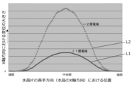
図4は、水晶片10に印加される電圧を一定にしたときの、水晶片10の長手方向における水晶片10の変位の大きさを示すグラフである。
FIG. 4 is a graph showing the magnitude of displacement of crystal blank 10 in the longitudinal direction of crystal blank 10 when the voltage applied to
同図の横軸は、水晶片10の長手方向(水晶の軸方向におけるX軸方向)における位置を示す。同図の縦軸は、X軸方向における変位の大きさを示す。同図の「L1」は励振電極が1層構造である場合の変位を示し、同図の「L2」は励振電極が2層構造である場合の変位を示す。ここで、同図の縦軸の変位の大きさは、アドミッタンスYとして示すことができる。アドミッタンスYとインピーダンスZとの間には、「Y=1/Z」の関係が成り立つ。すなわち、変位Xが大きくなると、インピーダンスZ(すなわち、CI値)が小さくなる。 The horizontal axis in the figure indicates the position in the longitudinal direction of the crystal piece 10 (the X-axis direction in the axial direction of the crystal). The vertical axis in the figure indicates the magnitude of displacement in the X-axis direction. "L1" in the figure indicates the displacement when the excitation electrode has a single-layer structure, and "L2" in the figure indicates the displacement when the excitation electrode has a two-layer structure. Here, the magnitude of displacement on the vertical axis of the figure can be indicated as admittance Y. FIG. A relationship of "Y=1/Z" holds between the admittance Y and the impedance Z. That is, as the displacement X increases, the impedance Z (that is, the CI value) decreases.
図4に示されるとおり、励振電極が2層構造である場合の変位は、同1層構造である場合の変位の約2-3倍大きい。特に、両構造における変位の差異は、X軸方向における端部から中央部に向かうに連れて大きくなる。これは、主振動の振動エネルギーが水晶片10の中央領域(両主面11,12の中央部112,122の間の領域)に集中し、同エネルギーが中央領域に閉じ込められていることを示す。
As shown in FIG. 4, the displacement when the excitation electrode has a two-layer structure is about 2-3 times larger than the displacement when it has the same one-layer structure. In particular, the difference in displacement between the two structures increases from the ends toward the center in the X-axis direction. This indicates that the vibrational energy of the main vibration is concentrated in the central region of crystal blank 10 (the region between
このように、第1励振電極211と第2励振電極221それぞれが、上層になるに連れて面積が小さくなる2層構造を有することで、主振動の振動エネルギーが水晶片10の中央領域に集中し、同振動エネルギーが中央領域に閉じ込められる。その結果、水晶片10の等価直列抵抗(CI:Crystal Impedance)値は、低減される。
In this way, the
●水晶発振器●
次いで、本発明にかかる水晶発振器の実施の形態について説明する。以下に説明する実施の形態において、先に説明した実施の形態と共通する部材の説明は、省略する。
● Crystal oscillator ●
Next, an embodiment of a crystal oscillator according to the present invention will be explained. In the embodiments described below, descriptions of members common to the previously described embodiments are omitted.
図5は、本発明にかかる水晶発振器の実施の形態を示す模式断面図である。 FIG. 5 is a schematic cross-sectional view showing an embodiment of a crystal oscillator according to the invention.
水晶発振器100は、例えば、温度補償型の水晶発振器(TCXO)である。水晶発振器100は、例えば、SMD型の水晶発振器である。水晶発振器100は、前述した水晶片10と電極20と導電性接着剤30とキャップ50と、筐体40Aと、回路60Aと、を有してなる。
筐体40Aは、水晶片10と回路60Aとを収容する。筐体40Aは、アルミナなどのセラミックスが積層された焼結体である。筐体40Aは、公知の水晶発振器の筐体(パッケージ)である。筐体40Aは、平面視において矩形状であり、上方に開口する箱状である。筐体40Aは、電極(不図示)と段部42と回路収容部43Aとを備える。
The
回路収容部43Aは、回路60Aを収容する。回路収容部43Aは、筐体40Aの底部の中央部に配置される。
The
回路60Aは、水晶片10(水晶振動子1)の振動周波数を制御する。回路60Aは、例えば、公知の温度補償回路である。
●まとめ
以上説明した各実施の形態によれば、本構造は、第1励振電極211と第2励振電極221それぞれが、上層になるに連れて面積が小さくなる2層構造を有する。そのため、本構造は、主振動の振動エネルギーを水晶片10の中央領域に集中させて、同振動エネルギーを中央領域に閉じ込める。その結果、水晶片10のCI値は、低減される。このように、本構造と、本構造を有する水晶振動子1と水晶発振器100とは、精密な水晶片10の加工を要することなくCI値を低減できる。
●Summary According to each of the embodiments described above, the present structure has a two-layer structure in which the area of each of the
また、CI値が低減されることで、CI値のばらつきの絶対値は小さくなる。すなわち、例えば、100Ωの平均CI値に対して50%増加した平均CI値は150Ωであるが、10Ωの平均CI値に対して50%増加した平均CI値は15オームである。また、例えば、100ΩのCI値に対して50Ω増加したCI値は150Ωであるが、10ΩのCI値に対して50Ω増加したCI値は60Ωである。このように、CI値がばらついたとしても、CI値は、規格内に収まり易くなる。その結果、本構造を有する水晶振動子1と水晶発振器100それぞれの生産性(歩留)は、向上する。また、この場合、本発明によるCI値の低減により、水晶片10の外縁部111,121のエッチング量は、低減される。その結果、水晶片10の生産性(歩留)は、向上する。
Also, by reducing the CI value, the absolute value of variation in the CI value becomes smaller. That is, for example, an average CI value increased by 50% for an average CI value of 100Ω is 150Ω, whereas an average CI value increased by 50% for an average CI value of 10Ω is 15 ohms. Also, for example, the CI value increased by 50Ω from the CI value of 100Ω is 150Ω, but the CI value increased by 50Ω from the CI value of 10Ω is 60Ω. In this way, even if the CI values vary, the CI values are likely to fall within the standard. As a result, the productivity (yield) of each of the
さらに、以上説明した実施の形態によれば、水晶片10の中央領域に主振動の振動エネルギーが閉じ込められることにより、水晶片10の端部、すなわち、接続電極212a,222aが配置される水晶片10の外縁部111への結合振動の影響は、抑制される。そのため、主振動に対する導電性接着剤30の影響は、抑制される。その結果、本構造を有する水晶振動子1と水晶発振器100それぞれの生産性(歩留)は、向上する。
Furthermore, according to the embodiments described above, the vibrational energy of the main vibration is confined in the central region of the
さらにまた、以上説明した実施の形態によれば、本構造を有する水晶振動子1を用いた水晶発振器100は、発振回路に組み込まれたとき、低励振動作を可能とし、発振の安定化に寄与する。
Furthermore, according to the embodiments described above, the
●その他
なお、本発明における水晶片は主振動として厚み滑り振動で励振すればよく、本発明における水晶片のカットは、ATカットに限定されない。すなわち、例えば、本発明における水晶片のカットは、BTカット、SCカット、ITカットでもよい。
●Others Note that the crystal blank in the present invention may be excited by thickness-shear vibration as the main vibration, and the cut of the crystal blank in the present invention is not limited to the AT cut. That is, for example, the cut of the crystal piece in the present invention may be BT cut, SC cut, or IT cut.
また、本発明における水晶片は、メサ型に限定されない。すなわち、例えば、本発明における水晶片は、平板型、ベベル型、逆メサ型、コンベックス型またはプラノコンベックス型のうち、いずれかの構造を有してもよい。この場合、本発明によるCI値の低減により、ベベル型においては、ベベル量が低減され、逆メサ型においては、水晶片の中央部凹部のエッチング量が低減される。その結果、水晶片の生産性(歩留)は、向上する。 Also, the crystal blank in the present invention is not limited to the mesa type. That is, for example, the crystal piece in the present invention may have any one of flat plate, bevel, inverted mesa, convex, and planoconvex structures. In this case, the reduction of the CI value according to the present invention reduces the amount of bevel in the bevel type, and reduces the amount of etching of the central concave portion of the crystal piece in the inverted mesa type. As a result, the productivity (yield) of crystal blanks is improved.
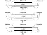
図6(a)-(c)は、本発明にかかる水晶振動子の別の実施の形態を示す模式断面図である。同図は、説明の便宜上、水晶片と電極それぞれの断面のみを示す。同図(a)は平板型の水晶片を示し、同図(b)はベベル型の水晶片を示し、同図(c)は逆メサ型の水晶片を示す。 6(a) to 6(c) are schematic cross-sectional views showing another embodiment of the crystal resonator according to the present invention. For convenience of explanation, this figure shows only the cross sections of the crystal piece and the electrodes. FIG. 1(a) shows a flat crystal piece, FIG. 1(b) shows a bevel crystal piece, and FIG. 1(c) shows an inverted mesa type crystal piece.
さらに、本発明における各水晶片の長辺(X軸方向に沿う辺)の長さは、2mm以下が望ましい。この構成によれば、本構造は、他の構造(例えば、水晶片の形状、電極の厚み・位置など)よりもCI値を低減させる。すなわち、本構造は、水晶片が小さいほど、他の構造よりもCI値を低減させ得る。 Furthermore, the length of the long side (the side along the X-axis direction) of each crystal piece in the present invention is desirably 2 mm or less. According to this configuration, this structure reduces the CI value more than other structures (for example, the shape of the crystal piece, the thickness and position of the electrodes, etc.). In other words, this structure can reduce the CI value more than other structures when the crystal piece is smaller.
さらにまた、本発明における水晶片は、フォトリソ工程により一括に形成されてもよく、あるいは、研磨・切断・表面エッチングなどの手法により個別に形成されもよい。 Furthermore, the crystal piece in the present invention may be formed collectively by a photolithography process, or may be formed individually by techniques such as polishing, cutting, and surface etching.
さらにまた、本発明における水晶片は、基本波モードの振動モードで励振してもよく、あるいは、高次(3次、5次)オーバトーンモードの振動モードで励振してもよい。 Furthermore, the crystal blank in the present invention may be excited in the vibration mode of the fundamental wave mode, or may be excited in the vibration mode of the higher-order (third or fifth order) overtone mode.
さらに、本発明における第1励振電極と第2励振電極それぞれは、両主面上に配置され、面積が順次小さくなるように積層される複数の電極部により構成されればよく、2層構造に限定されない。すなわち、例えば、本発明における第1励振電極と第2励振電極それぞれは、第2電極部上に積層して配置され、第2電極部の面積よりも小さい面積を有する第3電極部を備えてもよい。また、例えば、第1励振電極の積層数は、第2励振電極の積層数と異なってもよい。 Further, each of the first excitation electrode and the second excitation electrode in the present invention may be arranged on both main surfaces and may be composed of a plurality of electrode portions laminated so as to sequentially decrease in area, and has a two-layer structure. Not limited. That is, for example, each of the first excitation electrode and the second excitation electrode in the present invention includes a third electrode portion which is stacked on the second electrode portion and has an area smaller than that of the second electrode portion. good too. Further, for example, the number of stacked layers of the first excitation electrodes may be different from the number of stacked layers of the second excitation electrodes.
さらにまた、本発明における第2励振電極は、水晶片を挟んで、第1励振電極と非対称な構造を有してもよい。すなわち、例えば、本発明における第2励振電極は、平面視において、第1励振電極に対してX軸方向および/またはZ′軸方向にずれて配置されてもよい。 Furthermore, the second excitation electrode in the present invention may have a structure asymmetric with the first excitation electrode with the crystal blank interposed therebetween. That is, for example, the second excitation electrodes in the present invention may be arranged to be shifted in the X-axis direction and/or the Z'-axis direction with respect to the first excitation electrodes in plan view.
さらにまた、本発明における第1電極部と第2電極部とは、一体に構成されてもよい。すなわち、例えば、本発明における第1電極部と第2電極部とは1層の下地金属膜と金属膜とで構成されてもよい。この場合、電極外縁部は、例えば、1層の金属膜の外縁部が除去されることで形成されてもよい。 Furthermore, the first electrode portion and the second electrode portion in the present invention may be configured integrally. That is, for example, the first electrode portion and the second electrode portion in the present invention may be composed of one layer of base metal film and one layer of metal film. In this case, the outer edge of the electrode may be formed, for example, by removing the outer edge of one layer of metal film.
さらにまた、本発明における第1電極部の厚みと第2電極部の厚みとは、同じでもよく、あるいは、異なってもよい。ここで、各電極部の厚みは、例えば、蒸着前後の水晶片の周波数に基づいて算出される。また、各電極部の厚みは、例えば、プローブにより物理的に計測されてもよく、あるいは、透過光を用いて光学的に計測されてもよい。 Furthermore, the thickness of the first electrode portion and the thickness of the second electrode portion in the present invention may be the same or different. Here, the thickness of each electrode portion is calculated, for example, based on the frequency of the crystal piece before and after vapor deposition. Also, the thickness of each electrode portion may be physically measured using a probe, or may be optically measured using transmitted light.
さらにまた、本発明における下地金属膜は、水晶片と金属膜それぞれに親和性を有する金属製の膜であればよく、Cr膜に限定されない。すなわち、例えば、本発明における下地金属膜は、Cr,NiまたはWのうち、少なくとも1種の金属を含んでもよい。 Furthermore, the underlying metal film in the present invention is not limited to a Cr film as long as it is a metal film having an affinity for the crystal piece and the metal film. That is, for example, the underlying metal film in the present invention may contain at least one of Cr, Ni, and W.
さらにまた、本発明における金属膜は、水晶が励振可能な印加電圧を供給可能な金属製の膜であればよく、Au膜に限定されない。すなわち、例えば、本発明における金属膜は、Au,Ag,Cu,Al,W,Ni,またはMgのうち、少なくとも1種の金属を含んでもよい。 Furthermore, the metal film in the present invention is not limited to an Au film as long as it is a metal film that can supply an applied voltage that can excite crystal. That is, for example, the metal film in the present invention may contain at least one metal selected from Au, Ag, Cu, Al, W, Ni, and Mg.
さらにまた、本発明における第1励振電極と第2励振電極それぞれは、電極外縁部と、平面視において電極外縁部よりも内側の領域であって、電極外縁部を構成する金属よりも大きい質量を有する金属を含む電極中央部と、により構成されてもよい。すなわち、例えば、電極外縁部はAgやAl膜により構成され、電極中央部はAu膜により構成されてもよい。この構成において、1軸方向(例えば、X軸方向)における電極中央部の質量は、電極外縁部の質量よりも大きければよい。そのため、電極中央部の厚みは、電極外縁部の厚みと同じでもよく、あるいは、電極外縁部の厚みよりも薄くてもよい。また、例えば、電極中央部において、質量の大きい金属膜(例えば、Au膜)が、質量の小さい金属膜(例えば、Al膜)に覆われてもよい。これらの構成は、電極中央部の質量効果により、先に説明をした2層構造と同様に、主振動の振動エネルギーを水晶片の中央領域に集中させて、同振動エネルギーを中央領域に閉じ込める。 Furthermore, each of the first excitation electrode and the second excitation electrode in the present invention has an electrode outer edge portion and a region inside the electrode outer edge portion in plan view, and has a mass larger than the metal constituting the electrode outer edge portion. and an electrode center portion containing a metal having a That is, for example, the outer edge portion of the electrode may be made of Ag or Al film, and the central portion of the electrode may be made of Au film. In this configuration, the mass of the central portion of the electrode in one axial direction (eg, the X-axis direction) should be larger than the mass of the outer edge portion of the electrode. Therefore, the thickness of the central portion of the electrode may be the same as the thickness of the outer edge portion of the electrode, or may be thinner than the thickness of the outer edge portion of the electrode. Further, for example, a metal film with a large mass (eg, Au film) may be covered with a metal film with a small mass (eg, Al film) at the central portion of the electrode. These structures concentrate the vibrational energy of the main vibration in the central region of the crystal blank and confine the same vibrational energy in the central region, similar to the two-layer structure described above, due to the mass effect of the electrode central portion.
図7(a)-(c)は、本発明にかかる水晶振動子のさらに別の実施の形態を示す模式断面図である。同図は、説明の便宜上、水晶片と電極それぞれの断面のみを示す。同図の黒塗りの電極は、白抜きの電極よりも質量が大きい金属で構成される。同図(a)は電極外縁部と電極中央部それぞれの厚みが同じ構成を示し、同図(b)は電極中央部において質量の大きい金属膜が質量の小さい金属膜に覆われている構成を示し、同図(c)は電極外縁部の厚みが電極中央部の厚みよりも薄い構成を示す。 FIGS. 7(a)-(c) are schematic cross-sectional views showing still another embodiment of the crystal resonator according to the present invention. For convenience of explanation, this figure shows only the cross sections of the crystal piece and the electrodes. The black-filled electrodes in the figure are made of metal having a larger mass than the white-filled electrodes. (a) shows a configuration in which the outer edge portion and the central portion of the electrode have the same thickness. 4(c) shows a configuration in which the thickness of the outer edge of the electrode is thinner than the thickness of the central portion of the electrode.
さらにまた、本発明における各電極部の端面は、曲面でもよい。 Furthermore, the end surface of each electrode part in the present invention may be a curved surface.
さらにまた、平面視において、本発明における第2電極の4つの辺のうち、1つの辺は、第1電極の4つの辺のうち、1つの辺と重複してもよい。 Furthermore, in plan view, one of the four sides of the second electrode in the present invention may overlap with one of the four sides of the first electrode.
さらにまた、本発明にかかる水晶発振器は、温度補償型の水晶発振器に限定されない。すなわち、例えば、本発明にかかる水晶発振器は、電圧制御型の水晶発振器(VCXO)、恒温槽付の水晶発振器(OCXO)またはパッケージ型水晶発振器(SPXO)でもよい。 Furthermore, the crystal oscillator according to the present invention is not limited to a temperature compensated crystal oscillator. That is, for example, the crystal oscillator according to the present invention may be a voltage-controlled crystal oscillator (VCXO), an oven-controlled crystal oscillator (OCXO), or a packaged crystal oscillator (SPXO).
1 水晶振動子
10 水晶片
11 第1主面
12 第2主面
21 第1主面電極
211 第1励振電極
211a 第1電極部
211b 第2電極部
22 第2主面電極
221 第2励振電極
221a 第1電極部
221b 第2電極部
100 水晶発振器
1
Claims (17)
前記励振電極は、
前記水晶振動子を構成する平面視において矩形状の水晶片の主面上の少なくとも中央に配置され、平面視において矩形状の第1電極部により構成される電極外縁部と、
平面視において前記電極外縁部よりも内側の領域であり、前記第1電極部の一部と、前記第1電極部の前記一部に積層して配置される第2電極部と、により構成される矩形状の電極中央部と、
を含み、
前記第1電極部は、
前記励振電極として機能する金属膜と、
前記金属膜と前記水晶片との間に配置される下地として機能する下地金属膜と、
により構成され、
前記第2電極部は、前記励振電極として機能する金属膜により構成され、
前記第1電極部の第1面積は、前記電極外縁部の外縁により区画され、前記主面の面積よりも小さく、
前記第2電極部の第2面積は、前記第1面積よりも小さく、
前記電極中央部の単位面積当たりの質量は、前記電極外縁部の単位面積当たりの質量よりも大きく、
前記主面上に前記第1電極部を形成するステップと、
前記第1電極部の前記第1面積が固定された状態で、前記第2電極部の前記第2面積を変化させて、前記第1面積に対する前記第2面積の面積比のみにより定まるCI値と、前記面積比と、の関係を示すCI曲線を形成するステップと、
前記CI曲線において、前記CI値が極小値となる第1ボトム点と、前記第1ボトム点に対応する面積比よりも小さい面積比において前記CI値が極小値となる第2ボトム点とを特定するステップと、
前記第1面積に対する前記第2面積の面積比が前記第2ボトム点に対応する前記面積比となるように、前記第2電極部を形成するステップと、
を含む、
ことを特徴とする水晶振動子の励振電極の設計方法。 A method for designing an excitation electrode of a crystal oscillator, comprising:
The excitation electrode is
an electrode outer edge portion that is arranged at least in the center on the main surface of a crystal piece that is rectangular in plan view and that constitutes the crystal oscillator, and that is configured by a first electrode portion that is rectangular in plan view;
A region inside the outer edge of the electrode in a plan view, and is composed of a part of the first electrode part and a second electrode part laminated on the part of the first electrode part. a central portion of the rectangular electrode,
including
The first electrode part is
a metal film functioning as the excitation electrode;
a base metal film functioning as a base interposed between the metal film and the crystal piece;
is composed of
The second electrode section is composed of a metal film that functions as the excitation electrode,
the first area of the first electrode portion is defined by the outer edge of the electrode outer edge portion and is smaller than the area of the main surface;
the second area of the second electrode section is smaller than the first area,
the mass per unit area of the central portion of the electrode is greater than the mass per unit area of the outer edge portion of the electrode;
forming the first electrode portion on the main surface;
a CI value determined only by an area ratio of the second area to the first area by changing the second area of the second electrode part while the first area of the first electrode part is fixed; forming a CI curve showing the relationship between , and the area ratio ;
In the CI curve, specify a first bottom point at which the CI value is a minimum value and a second bottom point at which the CI value is a minimum value at an area ratio smaller than the area ratio corresponding to the first bottom point. and
forming the second electrode part such that the area ratio of the second area to the first area is the area ratio corresponding to the second bottom point;
including,
A method for designing an excitation electrode of a crystal oscillator, characterized by:
請求項1記載の水晶振動子の励振電極の設計方法。 The CI value at the second bottom point is less than or equal to the CI value at the first bottom point,
2. The method for designing an excitation electrode of a crystal oscillator according to claim 1.
請求項2記載の水晶振動子の励振電極の設計方法。 the CI value at the second bottom point is less than the CI value at the first bottom point;
3. The method for designing an excitation electrode of a crystal oscillator according to claim 2.
前記第2ボトム点は、前記面積比が80%以上90%未満の範囲内に存在する、
請求項1乃至3のいずれか1項に記載の水晶振動子の励振電極の設計方法。 The first bottom point exists within a range of the area ratio of 90% or more and less than 100%,
The second bottom point exists within a range of the area ratio of 80% or more and less than 90%.
4. The method for designing an excitation electrode of a crystal oscillator according to any one of claims 1 to 3.
請求項1記載の水晶振動子の励振電極の設計方法。 The angle between the end faces of each of the first electrode portion and the second electrode portion and the imaginary plane parallel to the main surface is 30°-90°.
2. The method for designing an excitation electrode of a crystal oscillator according to claim 1.
請求項5記載の水晶振動子の励振電極の設計方法。 Each of the metal film forming the first electrode portion and the metal film forming the second electrode portion is made of at least one metal selected from Au, Ag, Cu, Al, W, Ni, and Mg. to be
6. The method for designing an excitation electrode of a crystal oscillator according to claim 5.
請求項6記載の水晶振動子の励振電極の設計方法。 The metal film forming the second electrode portion is made of the same metal as the metal film forming the first electrode portion,
7. The method for designing an excitation electrode of a crystal oscillator according to claim 6.
請求項6記載の水晶振動子の励振電極の設計方法。 the base metal film contains at least one metal selected from Cr, Ni, and W;
7. The method for designing an excitation electrode of a crystal oscillator according to claim 6.
前記水晶片の主面上の少なくとも中央に配置される励振電極と、
を有してなる水晶振動子の製造方法であって、
前記励振電極は、請求項1乃至8のいずれか1項に記載の設計方法により設計される、
ことを特徴とする水晶振動子の製造方法。 a piece of crystal;
an excitation electrode arranged at least centrally on the main surface of the crystal piece;
A method for manufacturing a crystal oscillator comprising
The excitation electrode is designed by the design method according to any one of claims 1 to 8 ,
A method of manufacturing a crystal unit, characterized by:
請求項9記載の水晶振動子の製造方法。 The crystal piece excites thickness-shear vibration as a main vibration,
10. The method of manufacturing a crystal oscillator according to claim 9 .
第1主面と、
前記第1主面と反対側の面である第2主面と、
を備え、
前記励振電極は、
前記第1主面上に配置される第1励振電極と、
前記第2主面上に配置される第2励振電極と、
を含み、
前記第1励振電極と前記第2励振電極とは、前記水晶片を挟んで対称な構造を有するように形成される、
請求項9記載の水晶振動子の製造方法。 The crystal piece is
a first main surface;
a second main surface opposite to the first main surface;
with
The excitation electrode is
a first excitation electrode disposed on the first main surface;
a second excitation electrode disposed on the second main surface;
including
The first excitation electrode and the second excitation electrode are formed so as to have a symmetrical structure with the crystal piece interposed therebetween.
10. The method of manufacturing a crystal oscillator according to claim 9 .
第1主面と、
前記第1主面と反対側の面である第2主面と、
を備え、
前記励振電極は、
前記第1主面上に配置される第1励振電極と、
前記第2主面上に配置される第2励振電極と、
を含み、
前記第1励振電極と前記第2励振電極とは、前記水晶片を挟んで非対称な構造を有するように形成される、
請求項9記載の水晶振動子の製造方法。 The crystal piece is
a first main surface;
a second main surface opposite to the first main surface;
with
The excitation electrode is
a first excitation electrode disposed on the first main surface;
a second excitation electrode disposed on the second main surface;
including
The first excitation electrode and the second excitation electrode are formed to have an asymmetrical structure with the crystal piece sandwiched therebetween.
10. The method of manufacturing a crystal oscillator according to claim 9 .
請求項9記載の水晶振動子の製造方法。 The crystal piece has a substantially rectangular shape with a long side of 2 mm or less in plan view,
10. The method of manufacturing a crystal oscillator according to claim 9 .
請求項9記載の水晶振動子の製造方法。 The crystal piece is excited in any one of a fundamental wave mode, a third overtone mode, and a fifth overtone mode,
10. The method of manufacturing a crystal oscillator according to claim 9 .
請求項9記載の水晶振動子の製造方法。 the crystal piece has any one of a flat plate type, a bevel type, a mesa type, an inverted mesa type, a convex type, and a plano-convex type;
10. The method of manufacturing a crystal oscillator according to claim 9 .
前記水晶振動子の振動周波数を制御する回路と、
を有してなる水晶発振器の製造方法であって、
前記水晶振動子は、請求項9記載の製造方法により製造される、
ことを特徴とする水晶発振器の製造方法。 a crystal oscillator;
a circuit for controlling the oscillation frequency of the crystal oscillator;
A method for manufacturing a crystal oscillator , comprising:
The crystal oscillator is manufactured by the manufacturing method according to claim 9 ,
A method of manufacturing a crystal oscillator, characterized by:
前記励振電極は、The excitation electrode is
前記水晶振動子を構成する平面視において矩形状の水晶片の主面上の少なくとも中央に配置され、平面視において矩形状の第1電極部により構成される電極外縁部と、an electrode outer edge portion that is arranged at least in the center on the main surface of a crystal piece that is rectangular in plan view and that constitutes the crystal oscillator, and that is configured by a first electrode portion that is rectangular in plan view;
平面視において前記電極外縁部よりも内側の領域であり、前記第1電極部の一部と、前記第1電極部の前記一部に積層して配置される第2電極部と、により構成される矩形状の電極中央部と、A region inside the outer edge of the electrode in a plan view, and is composed of a part of the first electrode part and a second electrode part laminated on the part of the first electrode part. a central portion of the rectangular electrode,
を含み、including
前記第1電極部は、The first electrode part is
前記励振電極として機能する金属膜と、a metal film functioning as the excitation electrode;
前記金属膜と前記水晶片との間に配置される下地として機能する下地金属膜と、a base metal film functioning as a base interposed between the metal film and the crystal piece;
により構成され、is composed of
前記第2電極部は、前記励振電極として機能する金属膜により構成され、The second electrode section is composed of a metal film that functions as the excitation electrode,
前記第1電極部の第1面積は、前記電極外縁部の外縁により区画され、前記主面の面積よりも小さく、the first area of the first electrode portion is defined by the outer edge of the electrode outer edge portion and is smaller than the area of the main surface;
前記第2電極部の第2面積は、前記第1面積よりも小さく、the second area of the second electrode section is smaller than the first area,
前記電極中央部の単位面積当たりの質量は、前記電極外縁部の単位面積当たりの質量よりも大きく、the mass per unit area of the central portion of the electrode is greater than the mass per unit area of the outer edge portion of the electrode;
前記主面上に前記第1電極部を形成するステップと、forming the first electrode portion on the main surface;
前記第1電極部の前記第1面積が固定された状態で、前記第2電極部の前記第2面積を変化させて、前記第1面積に対する前記第2面積の面積比のみにより定まるCI値と、前記面積比と、の関係を示すCI曲線を形成するステップと、a CI value determined only by an area ratio of the second area to the first area by changing the second area of the second electrode part while the first area of the first electrode part is fixed; forming a CI curve showing the relationship between , and the area ratio;
前記CI曲線において、前記CI値が極小値となる第1ボトム点と、前記第1ボトム点に対応する面積比よりも小さい面積比において前記CI値が極小値となる第2ボトム点とを特定するステップと、In the CI curve, specify a first bottom point at which the CI value is a minimum value and a second bottom point at which the CI value is a minimum value at an area ratio smaller than the area ratio corresponding to the first bottom point. and
前記第1面積に対する前記第2面積の面積比が前記第2ボトム点に対応する前記面積比となるように、前記第2電極部を形成するステップと、forming the second electrode portion such that the area ratio of the second area to the first area is the area ratio corresponding to the second bottom point;
を含む、including,
ことを特徴とする水晶振動子の励振電極の製造方法。A method of manufacturing an excitation electrode for a crystal oscillator, characterized by:
Priority Applications (5)
| Application Number | Priority Date | Filing Date | Title |
|---|---|---|---|
| JP2020047607A JP7311152B2 (en) | 2020-03-18 | 2020-03-18 | Crystal oscillator electrode structure, crystal oscillator, crystal oscillator |
| PCT/JP2020/049056 WO2021186839A1 (en) | 2020-03-18 | 2020-12-28 | Electrode structure of quartz resonator, quartz resonator, quartz oscillator |
| CN202080096715.5A CN115136494A (en) | 2020-03-18 | 2020-12-28 | Electrode structure of crystal oscillator, and crystal oscillator |
| US17/906,267 US20230130678A1 (en) | 2020-03-18 | 2020-12-28 | Electrode structure of crystal unit, crystal unit, and crystal oscillator |
| TW110108543A TWI828973B (en) | 2020-03-18 | 2021-03-10 | Method of designing driven electrode of crystal unit, method of manufacturing crystal unit, method of manufacturing crystal oscillator, and method of manufacturing driven electrode of crystal unit |
Applications Claiming Priority (1)
| Application Number | Priority Date | Filing Date | Title |
|---|---|---|---|
| JP2020047607A JP7311152B2 (en) | 2020-03-18 | 2020-03-18 | Crystal oscillator electrode structure, crystal oscillator, crystal oscillator |
Publications (3)
| Publication Number | Publication Date |
|---|---|
| JP2021150761A JP2021150761A (en) | 2021-09-27 |
| JP2021150761A5 JP2021150761A5 (en) | 2022-12-02 |
| JP7311152B2 true JP7311152B2 (en) | 2023-07-19 |
Family
ID=77771144
Family Applications (1)
| Application Number | Title | Priority Date | Filing Date |
|---|---|---|---|
| JP2020047607A Active JP7311152B2 (en) | 2020-03-18 | 2020-03-18 | Crystal oscillator electrode structure, crystal oscillator, crystal oscillator |
Country Status (5)
| Country | Link |
|---|---|
| US (1) | US20230130678A1 (en) |
| JP (1) | JP7311152B2 (en) |
| CN (1) | CN115136494A (en) |
| TW (1) | TWI828973B (en) |
| WO (1) | WO2021186839A1 (en) |
Citations (7)
| Publication number | Priority date | Publication date | Assignee | Title |
|---|---|---|---|---|
| JP2005318477A (en) | 2004-04-30 | 2005-11-10 | Seiko Epson Corp | Piezo-electric vibrator, its electrode forming method, and piezo-electric device |
| JP2008005333A (en) | 2006-06-23 | 2008-01-10 | Daishinku Corp | Piezoelectric vibration device |
| JP2008047982A (en) | 2006-08-10 | 2008-02-28 | Daishinku Corp | Piezoelectric vibration device |
| JP2013255052A (en) | 2012-06-06 | 2013-12-19 | Seiko Epson Corp | Vibration element, vibrator, electronic device, electronic apparatus, mobile body, and manufacturing method of vibration element |
| JP2016019225A (en) | 2014-07-10 | 2016-02-01 | 富士通株式会社 | Crystal oscillator |
| JP2017192032A (en) | 2016-04-13 | 2017-10-19 | 日本電波工業株式会社 | Crystal resonator |
| JP2018042121A (en) | 2016-09-08 | 2018-03-15 | 株式会社村田製作所 | Crystal vibration element, manufacturing method thereof, crystal oscillator and manufacturing method thereof |
Family Cites Families (8)
| Publication number | Priority date | Publication date | Assignee | Title |
|---|---|---|---|---|
| JP2003273682A (en) * | 2002-03-15 | 2003-09-26 | Seiko Epson Corp | Frequency control method for piezoelectric vibrator, piezoelectric vibrator, and piezoelectric device |
| JP4036149B2 (en) * | 2003-07-03 | 2008-01-23 | セイコーエプソン株式会社 | Piezoelectric device leak detection method |
| JP2005159717A (en) * | 2003-11-26 | 2005-06-16 | Toyo Commun Equip Co Ltd | Piezoelectric vibrator and manufacturing method thereof |
| JP2013021667A (en) * | 2011-03-23 | 2013-01-31 | Nippon Dempa Kogyo Co Ltd | Crystal device |
| JP6552225B2 (en) * | 2015-03-12 | 2019-07-31 | エスアイアイ・クリスタルテクノロジー株式会社 | Piezoelectric vibrating reed and piezoelectric vibrator |
| JP6666166B2 (en) * | 2016-02-26 | 2020-03-13 | 京セラ株式会社 | Crystal element and crystal device |
| JP6791766B2 (en) * | 2017-01-17 | 2020-11-25 | 日本電波工業株式会社 | Piezoelectric vibrating pieces and piezoelectric devices |
| US20180241371A1 (en) * | 2017-02-21 | 2018-08-23 | Nihon Dempa Kogyo Co., Ltd. | Piezoelectric device |
-
2020
- 2020-03-18 JP JP2020047607A patent/JP7311152B2/en active Active
- 2020-12-28 US US17/906,267 patent/US20230130678A1/en active Pending
- 2020-12-28 CN CN202080096715.5A patent/CN115136494A/en active Pending
- 2020-12-28 WO PCT/JP2020/049056 patent/WO2021186839A1/en active Application Filing
-
2021
- 2021-03-10 TW TW110108543A patent/TWI828973B/en active
Patent Citations (7)
| Publication number | Priority date | Publication date | Assignee | Title |
|---|---|---|---|---|
| JP2005318477A (en) | 2004-04-30 | 2005-11-10 | Seiko Epson Corp | Piezo-electric vibrator, its electrode forming method, and piezo-electric device |
| JP2008005333A (en) | 2006-06-23 | 2008-01-10 | Daishinku Corp | Piezoelectric vibration device |
| JP2008047982A (en) | 2006-08-10 | 2008-02-28 | Daishinku Corp | Piezoelectric vibration device |
| JP2013255052A (en) | 2012-06-06 | 2013-12-19 | Seiko Epson Corp | Vibration element, vibrator, electronic device, electronic apparatus, mobile body, and manufacturing method of vibration element |
| JP2016019225A (en) | 2014-07-10 | 2016-02-01 | 富士通株式会社 | Crystal oscillator |
| JP2017192032A (en) | 2016-04-13 | 2017-10-19 | 日本電波工業株式会社 | Crystal resonator |
| JP2018042121A (en) | 2016-09-08 | 2018-03-15 | 株式会社村田製作所 | Crystal vibration element, manufacturing method thereof, crystal oscillator and manufacturing method thereof |
Also Published As
| Publication number | Publication date |
|---|---|
| TW202137698A (en) | 2021-10-01 |
| CN115136494A (en) | 2022-09-30 |
| JP2021150761A (en) | 2021-09-27 |
| TWI828973B (en) | 2024-01-11 |
| WO2021186839A1 (en) | 2021-09-23 |
| US20230130678A1 (en) | 2023-04-27 |
Similar Documents
| Publication | Publication Date | Title |
|---|---|---|
| JP5632627B2 (en) | Quartz crystal | |
| US7973458B2 (en) | Piezoelectric vibrating pieces having progressively narrowed vibrating arms | |
| JP5912557B2 (en) | Tuning fork type piezoelectric vibrating piece and piezoelectric device | |
| US7902721B2 (en) | Crystal resonator | |
| EP2051375B1 (en) | Quartz crystal device for surface mounting | |
| JP5088613B2 (en) | Frequency adjusting method for vibration device, vibration device and electronic device | |
| JP2010004456A (en) | Piezoelectric vibrating piece and piezoelectric device | |
| CN109891745B (en) | Tuning fork vibrator and method for manufacturing tuning fork vibrator | |
| JP7311152B2 (en) | Crystal oscillator electrode structure, crystal oscillator, crystal oscillator | |
| WO2014167933A1 (en) | Tuning-fork-type crystal oscillator and crystal oscillation device | |
| JP4558433B2 (en) | Crystal oscillator | |
| JP4196641B2 (en) | Ultra-thin piezoelectric device and manufacturing method thereof | |
| WO2014097945A1 (en) | Tuning-fork-type quartz vibrating piece | |
| JP5495080B2 (en) | Frequency adjusting method for vibration device, vibration device, and electronic device | |
| JP2002141765A (en) | Piezoelectric substrate, piezoelectric vibrator and piezoelectric device mounting it | |
| JP5839997B2 (en) | Manufacturing method of crystal unit | |
| EP4311108A1 (en) | Quartz resonator and method for producing same | |
| JP2020065223A (en) | Tuning fork type piezoelectric vibrating piece and tuning fork type piezoelectric vibrator using tuning fork type piezoelectric vibrating piece | |
| JP2017157934A (en) | Tuning-fork piezoelectric vibration piece and piezoelectric device using tuning-fork piezoelectric vibration piece | |
| JP7380067B2 (en) | A tuning fork type piezoelectric vibrating piece and a tuning fork type piezoelectric vibrator using the tuning fork type piezoelectric vibrating piece | |
| JP2023003011A (en) | Vibration element, vibrator, and electronic device | |
| JP2023031666A (en) | Vibration element and oscillator | |
| JP2019145896A (en) | Tuning-fork type piezoelectric oscillation piece and tuning-fork type piezoelectric oscillator using the same | |
| JP5872660B2 (en) | Quartz crystal | |
| JP2019153973A (en) | Tuning fork type piezoelectric vibrating piece |
Legal Events
| Date | Code | Title | Description |
|---|---|---|---|
| A521 | Request for written amendment filed |
Free format text: JAPANESE INTERMEDIATE CODE: A523 Effective date: 20220720 |
|
| A621 | Written request for application examination |
Free format text: JAPANESE INTERMEDIATE CODE: A621 Effective date: 20220720 |
|
| A871 | Explanation of circumstances concerning accelerated examination |
Free format text: JAPANESE INTERMEDIATE CODE: A871 Effective date: 20220720 |
|
| A131 | Notification of reasons for refusal |
Free format text: JAPANESE INTERMEDIATE CODE: A131 Effective date: 20230214 |
|
| A521 | Request for written amendment filed |
Free format text: JAPANESE INTERMEDIATE CODE: A523 Effective date: 20230320 |
|
| TRDD | Decision of grant or rejection written | ||
| A01 | Written decision to grant a patent or to grant a registration (utility model) |
Free format text: JAPANESE INTERMEDIATE CODE: A01 Effective date: 20230620 |
|
| A61 | First payment of annual fees (during grant procedure) |
Free format text: JAPANESE INTERMEDIATE CODE: A61 Effective date: 20230629 |
|
| R150 | Certificate of patent or registration of utility model |
Ref document number: 7311152 Country of ref document: JP Free format text: JAPANESE INTERMEDIATE CODE: R150 |