JP7304492B2 - Flexible printed wiring board and manufacturing method thereof - Google Patents
Flexible printed wiring board and manufacturing method thereof Download PDFInfo
- Publication number
- JP7304492B2 JP7304492B2 JP2022535005A JP2022535005A JP7304492B2 JP 7304492 B2 JP7304492 B2 JP 7304492B2 JP 2022535005 A JP2022535005 A JP 2022535005A JP 2022535005 A JP2022535005 A JP 2022535005A JP 7304492 B2 JP7304492 B2 JP 7304492B2
- Authority
- JP
- Japan
- Prior art keywords
- wiring
- plating layer
- flexible printed
- layer
- wiring board
- Prior art date
- Legal status (The legal status is an assumption and is not a legal conclusion. Google has not performed a legal analysis and makes no representation as to the accuracy of the status listed.)
- Active
Links
Images


Classifications
-
- H—ELECTRICITY
- H05—ELECTRIC TECHNIQUES NOT OTHERWISE PROVIDED FOR
- H05K—PRINTED CIRCUITS; CASINGS OR CONSTRUCTIONAL DETAILS OF ELECTRIC APPARATUS; MANUFACTURE OF ASSEMBLAGES OF ELECTRICAL COMPONENTS
- H05K1/00—Printed circuits
- H05K1/02—Details
- H05K1/0296—Conductive pattern lay-out details not covered by sub groups H05K1/02 - H05K1/0295
-
- H—ELECTRICITY
- H05—ELECTRIC TECHNIQUES NOT OTHERWISE PROVIDED FOR
- H05K—PRINTED CIRCUITS; CASINGS OR CONSTRUCTIONAL DETAILS OF ELECTRIC APPARATUS; MANUFACTURE OF ASSEMBLAGES OF ELECTRICAL COMPONENTS
- H05K3/00—Apparatus or processes for manufacturing printed circuits
- H05K3/10—Apparatus or processes for manufacturing printed circuits in which conductive material is applied to the insulating support in such a manner as to form the desired conductive pattern
- H05K3/18—Apparatus or processes for manufacturing printed circuits in which conductive material is applied to the insulating support in such a manner as to form the desired conductive pattern using precipitation techniques to apply the conductive material
-
- C—CHEMISTRY; METALLURGY
- C25—ELECTROLYTIC OR ELECTROPHORETIC PROCESSES; APPARATUS THEREFOR
- C25D—PROCESSES FOR THE ELECTROLYTIC OR ELECTROPHORETIC PRODUCTION OF COATINGS; ELECTROFORMING; APPARATUS THEREFOR
- C25D21/00—Processes for servicing or operating cells for electrolytic coating
- C25D21/12—Process control or regulation
-
- C—CHEMISTRY; METALLURGY
- C25—ELECTROLYTIC OR ELECTROPHORETIC PROCESSES; APPARATUS THEREFOR
- C25D—PROCESSES FOR THE ELECTROLYTIC OR ELECTROPHORETIC PRODUCTION OF COATINGS; ELECTROFORMING; APPARATUS THEREFOR
- C25D3/00—Electroplating: Baths therefor
- C25D3/02—Electroplating: Baths therefor from solutions
-
- C—CHEMISTRY; METALLURGY
- C25—ELECTROLYTIC OR ELECTROPHORETIC PROCESSES; APPARATUS THEREFOR
- C25D—PROCESSES FOR THE ELECTROLYTIC OR ELECTROPHORETIC PRODUCTION OF COATINGS; ELECTROFORMING; APPARATUS THEREFOR
- C25D5/00—Electroplating characterised by the process; Pretreatment or after-treatment of workpieces
- C25D5/02—Electroplating of selected surface areas
-
- C—CHEMISTRY; METALLURGY
- C25—ELECTROLYTIC OR ELECTROPHORETIC PROCESSES; APPARATUS THEREFOR
- C25D—PROCESSES FOR THE ELECTROLYTIC OR ELECTROPHORETIC PRODUCTION OF COATINGS; ELECTROFORMING; APPARATUS THEREFOR
- C25D5/00—Electroplating characterised by the process; Pretreatment or after-treatment of workpieces
- C25D5/10—Electroplating with more than one layer of the same or of different metals
-
- C—CHEMISTRY; METALLURGY
- C25—ELECTROLYTIC OR ELECTROPHORETIC PROCESSES; APPARATUS THEREFOR
- C25D—PROCESSES FOR THE ELECTROLYTIC OR ELECTROPHORETIC PRODUCTION OF COATINGS; ELECTROFORMING; APPARATUS THEREFOR
- C25D7/00—Electroplating characterised by the article coated
-
- H—ELECTRICITY
- H05—ELECTRIC TECHNIQUES NOT OTHERWISE PROVIDED FOR
- H05K—PRINTED CIRCUITS; CASINGS OR CONSTRUCTIONAL DETAILS OF ELECTRIC APPARATUS; MANUFACTURE OF ASSEMBLAGES OF ELECTRICAL COMPONENTS
- H05K1/00—Printed circuits
- H05K1/02—Details
- H05K1/0277—Bendability or stretchability details
- H05K1/028—Bending or folding regions of flexible printed circuits
-
- H—ELECTRICITY
- H05—ELECTRIC TECHNIQUES NOT OTHERWISE PROVIDED FOR
- H05K—PRINTED CIRCUITS; CASINGS OR CONSTRUCTIONAL DETAILS OF ELECTRIC APPARATUS; MANUFACTURE OF ASSEMBLAGES OF ELECTRICAL COMPONENTS
- H05K1/00—Printed circuits
- H05K1/02—Details
- H05K1/03—Use of materials for the substrate
- H05K1/0393—Flexible materials
-
- H—ELECTRICITY
- H05—ELECTRIC TECHNIQUES NOT OTHERWISE PROVIDED FOR
- H05K—PRINTED CIRCUITS; CASINGS OR CONSTRUCTIONAL DETAILS OF ELECTRIC APPARATUS; MANUFACTURE OF ASSEMBLAGES OF ELECTRICAL COMPONENTS
- H05K2203/00—Indexing scheme relating to apparatus or processes for manufacturing printed circuits covered by H05K3/00
- H05K2203/03—Metal processing
- H05K2203/0307—Providing micro- or nanometer scale roughness on a metal surface, e.g. by plating of nodules or dendrites
-
- H—ELECTRICITY
- H05—ELECTRIC TECHNIQUES NOT OTHERWISE PROVIDED FOR
- H05K—PRINTED CIRCUITS; CASINGS OR CONSTRUCTIONAL DETAILS OF ELECTRIC APPARATUS; MANUFACTURE OF ASSEMBLAGES OF ELECTRICAL COMPONENTS
- H05K2203/00—Indexing scheme relating to apparatus or processes for manufacturing printed circuits covered by H05K3/00
- H05K2203/07—Treatments involving liquids, e.g. plating, rinsing
- H05K2203/0703—Plating
- H05K2203/0723—Electroplating, e.g. finish plating
Landscapes
- Engineering & Computer Science (AREA)
- Chemical & Material Sciences (AREA)
- Chemical Kinetics & Catalysis (AREA)
- Electrochemistry (AREA)
- Materials Engineering (AREA)
- Metallurgy (AREA)
- Organic Chemistry (AREA)
- Microelectronics & Electronic Packaging (AREA)
- Manufacturing & Machinery (AREA)
- Automation & Control Theory (AREA)
- Manufacturing Of Printed Wiring (AREA)
Description
本開示は、フレキシブルプリント配線板及びその製造方法に関する。本出願は、2020年7月8日出願の日本出願第2020-117888号に基づく優先権を主張し、前記日本出願に記載された全ての記載内容を援用するものである。 TECHNICAL FIELD The present disclosure relates to flexible printed wiring boards and manufacturing methods thereof. This application claims priority based on Japanese application No. 2020-117888 filed on July 8, 2020, and incorporates all the descriptions described in the Japanese application.
フレキシブルプリント配線板は、様々な電子機器の回路を構成するために広く利用されている。近年、電子機器の小型化に伴い、フレキシブルプリント配線板の小型化及びその配線密度の増大が著しい。 Flexible printed wiring boards are widely used to form circuits of various electronic devices. In recent years, with the miniaturization of electronic equipment, the miniaturization of flexible printed wiring boards and the increase in wiring density thereof have been remarkable.
このような小型の配線板として、基板と、この基板の表面に配置される第1めっき層及び第2めっき層を含む配線とを備え、第2めっき層の表面粗さが1nm~600nmである配線板が提案されている。この配線板によれば、第2めっき層と、この第2めっき層を覆う絶縁膜との密着力を増大することができる(特開2019-186518号公報参照)。 Such a small wiring board includes a substrate and wiring including a first plating layer and a second plating layer arranged on the surface of the substrate, and the surface roughness of the second plating layer is 1 nm to 600 nm. A wiring board has been proposed. According to this wiring board, the adhesion between the second plating layer and the insulating film covering the second plating layer can be increased (see JP-A-2019-186518).
本開示の一態様に係るフレキシブルプリント配線板は、ベースフィルムと、上記ベースフィルムの表面に配置される複数の配線とを備えるフレキシブルプリント配線板であって、上記配線は、その長手方向に沿った先端面及び上記長手方向に沿った2つの側面を有し、上記側面の算術平均粗さRaが0.05μm以上2.0μm以下であり、上記配線の平均高さが40μm以上120μm以下であり、上記配線の平均間隔が1μm以上30μm以下である。 A flexible printed wiring board according to an aspect of the present disclosure is a flexible printed wiring board including a base film and a plurality of wirings arranged on the surface of the base film, wherein the wirings are along the longitudinal direction It has a tip surface and two side surfaces along the longitudinal direction, the arithmetic mean roughness Ra of the side surface is 0.05 μm or more and 2.0 μm or less, the average height of the wiring is 40 μm or more and 120 μm or less, The average spacing of the wiring is 1 μm or more and 30 μm or less.
本開示の別の態様に係るフレキシブルプリント配線板の製造方法は、ベースフィルムと、上記ベースフィルムの表面に配置される複数の配線とを備えるフレキシブルプリント配線板の製造方法であって、上記配線は、その長手方向に沿った先端面及び上記長手方向に沿った2つの側面を有し、上記側面の算術平均粗さRaが0.05μm以上2.0μm以下であり、上記配線の平均高さが40μm以上120μm以下であり、上記配線の平均間隔が1μm以上30μm以下であり、表面に導電性下地層が積層されたベースフィルムを準備し、レジストパターンを用いて第1めっき液中にて上記導電性下地層上に電気めっきすることにより第1めっき層を形成する第1めっき工程と、上記レジストパターン及び上記導電性下地層における上記第1めっき層の非積層領域を除去する工程と、上記除去する工程の後、第2めっき液中にて上記第1めっき層に電気めっきすることにより、第2めっき層を形成する第2めっき工程とを備え、上記第2めっき液が、2500以上8000以下の数平均分子量を有するポリエチレングリコールを含有し、上記第2めっき工程では、上記側面の算術平均粗さRaが0.05μm以上2.0μm以下となるように上記電気めっきの電流密度を調整する。
A method for manufacturing a flexible printed wiring board according to another aspect of the present disclosure is a method for manufacturing a flexible printed wiring board including a base film and a plurality of wirings arranged on a surface of the base film, wherein the wirings are , has a tip surface along the longitudinal direction and two side surfaces along the longitudinal direction, the arithmetic average roughness Ra of the side surface is 0.05 μm or more and 2.0 μm or less, and the average height of the wiring is A base film having a thickness of 40 μm or more and 120 μm or less, an average spacing of the wirings of 1 μm or more and 30 μm or less, and having a conductive underlayer laminated on the surface thereof is prepared. a first plating step of forming a first plating layer by electroplating on a conductive underlayer; a step of removing a non-laminated region of the first plating layer in the resist pattern and the conductive underlayer; and a second plating step of forming a second plating layer by electroplating the first plating layer in a second plating solution, after the step of In the second plating step, the current density of the electroplating is adjusted so that the arithmetic mean roughness Ra of the side surface is 0.05 μm or more and 2.0 μm or less.
[本開示が解決しようとする課題]
上記特許文献の配線板では、配線の間隔が比較的小さくかつ配線の高さが比較的大きくなると、隣接する配線が接触し、短絡が発生するおそれがある。[Problems to be Solved by the Present Disclosure]
In the wiring board disclosed in the above patent document, if the distance between the wirings is relatively small and the height of the wirings is relatively large, the adjacent wirings may come into contact with each other, causing a short circuit.
本開示は、配線を覆う絶縁膜との接着性に優れ、短絡が抑制されたフレキシブルプリント配線板及びその製造方法を提供することを目的とする。 An object of the present disclosure is to provide a flexible printed wiring board that has excellent adhesiveness to an insulating film that covers wiring and that suppresses short circuits, and a method for manufacturing the same.
[本開示の効果]
本開示の一態様に係るフレキシブルプリント配線板は、絶縁膜との接着性に優れ、しかも短絡が抑制されている。本開示の別の態様に係るフレキシブルプリント配線板の製造方法は、絶縁膜との接着性に優れ、しかも短絡が抑制されたフレキシブルプリント配線板を製造することができる。[Effect of the present disclosure]
A flexible printed wiring board according to an aspect of the present disclosure has excellent adhesiveness to an insulating film and suppresses short circuits. A method for manufacturing a flexible printed wiring board according to another aspect of the present disclosure can manufacture a flexible printed wiring board that has excellent adhesion to an insulating film and that suppresses short circuits.
[本開示の実施形態の説明]
本開示の一態様に係るフレキシブルプリント配線板は、ベースフィルムと、上記ベースフィルムの表面に配置される複数の配線とを備えるフレキシブルプリント配線板であって、上記配線は、その長手方向に沿った先端面及び上記長手方向に沿った2つの側面を有し、上記側面の算術平均粗さRaが0.05μm以上2.0μm以下であり、上記配線の平均高さが40μm以上120μm以下であり、上記配線の平均間隔が1μm以上30μm以下である。[Description of Embodiments of the Present Disclosure]
A flexible printed wiring board according to an aspect of the present disclosure is a flexible printed wiring board including a base film and a plurality of wirings arranged on the surface of the base film, wherein the wirings are along the longitudinal direction It has a tip surface and two side surfaces along the longitudinal direction, the arithmetic mean roughness Ra of the side surface is 0.05 μm or more and 2.0 μm or less, the average height of the wiring is 40 μm or more and 120 μm or less, The average spacing of the wiring is 1 μm or more and 30 μm or less.
当該フレキシブルプリント配線板では、側面の算術平均粗さRaが上記範囲内であり、かつ配線の平均高さ及び平均間隔が上記範囲であるので短絡を抑制することができる。加えて、配線を覆うように絶縁膜が積層される場合、この絶縁膜と配線との接着性を大きくすることができる。よって、当該フレキシブルプリント配線板は、絶縁膜との接着性に優れ、しかも短絡が抑制されている。 In the flexible printed wiring board, since the arithmetic average roughness Ra of the side surface is within the above range and the average height and average spacing of the wiring are within the above range, short circuits can be suppressed. In addition, when an insulating film is laminated so as to cover the wiring, the adhesion between this insulating film and the wiring can be increased. Therefore, the flexible printed wiring board has excellent adhesiveness to the insulating film, and further suppresses short circuits.
上記先端面の算術平均粗さRaが0.05μm以上2.0μm以下であってもよい。 The arithmetic mean roughness Ra of the tip surface may be 0.05 μm or more and 2.0 μm or less.
上記先端面の算術平均粗さRaが上記範囲内であることで、絶縁膜と配線との接着性をより大きくすることができる。よって、当該フレキシブルプリント配線板が、より絶縁膜との接着性に優れる。 When the arithmetic mean roughness Ra of the tip surface is within the above range, the adhesion between the insulating film and the wiring can be further increased. Therefore, the flexible printed wiring board is more excellent in adhesion to the insulating film.
上記配線の平均線幅が5μm以上30μm以下であってもよい。 An average line width of the wiring may be 5 μm or more and 30 μm or less.
平均線幅が上記範囲内である配線においても絶縁膜と配線との接着性をより大きくすることができる。よって、当該フレキシブルプリント配線板の優位性が高まる。 Even in the wiring having the average line width within the above range, the adhesion between the insulating film and the wiring can be increased. Therefore, the superiority of the flexible printed wiring board is enhanced.
上記配線の平均高さが40μm以上60μm以下であってもよい。 The average height of the wiring may be 40 μm or more and 60 μm or less.
平均高さが上記範囲内であるので、絶縁膜と配線との接着性をより大きくし、かつ短絡を抑制することができる。よって、フレキシブルプリント配線板の優位性が高まる。 Since the average height is within the above range, it is possible to increase the adhesiveness between the insulating film and the wiring and to suppress short circuits. Therefore, the superiority of the flexible printed wiring board increases.
上記配線の幅は、上記長手方向に垂直な断面において、上記ベースフィルムの上記表面から上記先端面に向けて大きくなる。この特徴によると、配線を覆う絶縁膜との接着性に優れる。 The width of the wiring increases from the surface of the base film toward the tip surface in a cross section perpendicular to the longitudinal direction. According to this feature, the adhesiveness to the insulating film covering the wiring is excellent.
上記配線は、上記ベースフィルムの上記表面に積層される第1導電性下地層と、上記第1導電性下地層における上記ベースフィルムとは反対の表面に積層される第1めっき層と、上記第1導電性下地層の両側面及び上記第1めっき層の第1導電性下地層とは反対の側の表面及び両側面を覆うように積層される第2めっき層を含み、上記第2めっき層の先端面と側面がそれぞれ上記配線の上記先端面と上記側面に相当する。 The wiring includes a first conductive underlayer laminated on the surface of the base film, a first plating layer laminated on the surface of the first conductive underlayer opposite to the base film, and the first 1 a second plating layer laminated so as to cover both side surfaces of the conductive base layer and the surface and both side surfaces of the first plating layer opposite to the first conductive base layer, the second plating layer correspond to the tip surface and the side surface of the wiring, respectively.
上記第1めっき層の側面に垂直方向の上記第2めっき層の厚みが、上記ベースフィルムの上記表面と上記第2めっき層との接触面から先端面に向けて大きくなる。この特徴によると、配線を覆う絶縁膜との接着性に優れる。 The thickness of the second plating layer in the direction perpendicular to the side surface of the first plating layer increases from the contact surface between the surface of the base film and the second plating layer toward the tip surface. According to this feature, the adhesiveness to the insulating film covering the wiring is excellent.
上記配線は、上記ベースフィルムの上記表面に積層される第2導電性下地層と、上記第2導電性下地層における上記ベースフィルムとは反対の表面に積層される第3めっき層を含み、上記第3めっき層の先端面が上記配線の上記先端面に相当し、上記第2導電性下地層の側面及び上記第3めっき層の側面が上記配線の上記側面に相当する。
The wiring includes a second conductive underlayer laminated on the surface of the base film, and a third plating layer laminated on the surface of the second conductive underlayer opposite to the base film, The tip surface of the third plating layer corresponds to the tip surface of the wiring, and the side surface of the second conductive base layer and the side surface of the third plating layer correspond to the side surface of the wiring.
本開示の別の態様に係るフレキシブルプリント配線板の製造方法は、ベースフィルムと、上記ベースフィルムの表面に配置される複数の配線とを備えるフレキシブルプリント配線板の製造方法であって、上記配線は、その長手方向に沿った先端面及び上記長手方向に沿った2つの側面を有し、上記側面の算術平均粗さRaが0.05μm以上2.0μm以下であり、上記配線の平均高さが40μm以上120μm以下であり、上記配線の平均間隔が1μm以上30μm以下であり、表面に導電性下地層が積層されたベースフィルムを準備し、レジストパターンを用いて第1めっき液中にて上記導電性下地層上に電気めっきすることにより第1めっき層を形成する第1めっき工程と、上記レジストパターン及び上記導電性下地層における上記第1めっき層の非積層領域を除去する工程と、上記除去する工程の後、第2めっき液中にて上記第1めっき層に電気めっきすることにより、第2めっき層を形成する第2めっき工程とを備え、上記第2めっき液が、2500以上8000以下の数平均分子量を有するポリエチレングリコールを含有し、上記第2めっき工程では、上記側面の算術平均粗さRaが0.05μm以上2.0μm以下となるように上記電気めっきの電流密度を調整する。
A method for manufacturing a flexible printed wiring board according to another aspect of the present disclosure is a method for manufacturing a flexible printed wiring board including a base film and a plurality of wirings arranged on a surface of the base film, wherein the wirings are , has a tip surface along the longitudinal direction and two side surfaces along the longitudinal direction, the arithmetic average roughness Ra of the side surface is 0.05 μm or more and 2.0 μm or less, and the average height of the wiring is A base film having a thickness of 40 μm or more and 120 μm or less, an average spacing of the wirings of 1 μm or more and 30 μm or less, and having a conductive underlayer laminated on the surface thereof is prepared. a first plating step of forming a first plating layer by electroplating on a conductive underlayer; a step of removing a non-laminated region of the first plating layer in the resist pattern and the conductive underlayer; and a second plating step of forming a second plating layer by electroplating the first plating layer in a second plating solution, after the step of In the second plating step, the current density of the electroplating is adjusted so that the arithmetic mean roughness Ra of the side surface is 0.05 μm or more and 2.0 μm or less.
当該フレキシブルプリント配線板の製造方法によれば、上述した当該フレキシブルプリント配線板を製造することができる。すなわち、配線と配線を覆う絶縁膜との接着性に優れ、しかも短絡が抑制されたフレキシブルプリント配線板を製造することができる。 According to the method for manufacturing the flexible printed wiring board, the flexible printed wiring board described above can be manufactured. That is, it is possible to manufacture a flexible printed wiring board which has excellent adhesiveness between the wiring and the insulating film covering the wiring, and in which short circuits are suppressed.
上記第2めっき工程では、上記電流密度を2段階で調整するとよい。 In the second plating step, the current density is preferably adjusted in two steps.
第2めっき工程において電流密度を2段階で調整することで、算術平均粗さRaを上記範囲内に調整することが容易になる。 By adjusting the current density in two stages in the second plating step, it becomes easy to adjust the arithmetic mean roughness Ra within the above range.
本明細書でいう「高さ方向」とは、配線が形成されるベースフィルムの面に垂直な方向を意味する。「配線の平均高さ」とは、1本の配線の任意の十点において測定した高さの平均値を意味する。「高さ」とは、ベースフィルムの面に垂直な方向におけるベースフィルムから配線の上端縁までの間の距離を意味する。「高さ」は「厚み」に相当する。 The "height direction" as used herein means a direction perpendicular to the surface of the base film on which the wiring is formed. “Average height of wiring” means an average value of heights measured at arbitrary ten points of one wiring. "Height" means the distance between the base film and the top edge of the wiring in the direction perpendicular to the plane of the base film. "Height" corresponds to "thickness".
配線の「間隔」とは、対向する2本の配線の隣接面間の距離を意味する。「平均間隔」とは、長手方向に垂直な配線断面をミクロトーム等の断面加工装置で露出させ任意の十点の断面観察による隣接面間の距離を平均した値を意味する。配線の「線幅」とは、配線における長手方向と垂直な方向の幅の寸法を意味する。「平均線幅」とは、配線断面をミクロトーム等の断面加工装置で露出させ任意の十点の断面観察による各最大幅を平均した値を意味する。
ただし、各配線間を接続するためのビア(スルーホール、ブラインドビア、フィルドビア)を有するランド部分、実装部品との接続するランド部分、他のプリント基板やコネクターとの接続するためのランド部分等のランド部分については、上記にて規定する「高さ」、「線幅」「間隔」から除外するものとする。The “spacing” between wirings means the distance between adjacent surfaces of two wirings facing each other. The "average distance" means a value obtained by averaging the distance between adjacent surfaces obtained by exposing a wiring cross section perpendicular to the longitudinal direction with a cross-section processing apparatus such as a microtome and observing arbitrary ten cross-sections. The "line width" of the wiring means the dimension of the width in the direction perpendicular to the longitudinal direction of the wiring. The "average line width" means a value obtained by averaging the maximum widths obtained by exposing a wiring cross section with a cross-section processing apparatus such as a microtome and observing arbitrary ten cross-sections.
However, land parts with vias (through holes, blind vias, filled vias) for connecting wiring, land parts connecting with mounted parts, land parts for connecting with other printed circuit boards and connectors, etc. The land portion shall be excluded from the "height", "line width" and "gap" defined above.
「側面の算術平均粗さRa」とは、各配線における各側面全体の算術平均粗さRaを意味する。「先端面の算術平均粗さRa」とは、各配線における先端面全体の算術平均粗さRaを意味する。ここでいう「算術平均粗さRa」とは、配線の側面又は先端面における任意の5箇所の算術平均粗さRaを測定し、これの平均値をいう。任意の5箇所の各算術平均粗さRaとは、各箇所において、粗さ曲線からその平均線の方向に位置0から位置Lまで基準長さ(L)だけを抜き取り、この抜取り部分の平均線の方向にX軸を、縦倍率の方向にY軸を取り、粗さ曲線をy=f(x)で表したときに、下記式(1)によって求められる値をマイクロメートル(μm)で表したものを意味する。具体的な測定方法は実施例で説明する。
The “arithmetic average roughness Ra of the side surface” means the arithmetic average roughness Ra of the entire side surface of each wiring. “Arithmetic mean roughness Ra of the tip surface” means the arithmetic mean roughness Ra of the entire tip surface of each wiring. The term "arithmetic mean roughness Ra" as used herein refers to the average value of the arithmetic mean roughnesses Ra measured at arbitrary five locations on the side surface or tip end face of the wiring. Each of the five arbitrary arithmetic mean roughness Ra means that at each point, only the reference length (L) is extracted from the roughness curve in the direction of the average line from position 0 to position L, and the average line of this extracted part Taking the X-axis in the direction of and the Y-axis in the direction of longitudinal magnification, and expressing the roughness curve as y = f (x), the value obtained by the following formula (1) is expressed in micrometers (μm) means what was done. A specific measuring method will be described in Examples.

[本開示の実施形態の詳細]
以下、本開示に係るフレキシブルプリント配線板及びその製造方法の実施形態について図面を参照しつつ詳説する。なお、本実施形態において「表面」とは、ベースフィルムの高さ方向のうち、配線が積層される側の面を指すものであり、本実施形態の表裏がフレキシブルプリント配線板の使用状態における表裏を決定するものではない。[Details of the embodiment of the present disclosure]
EMBODIMENT OF THE INVENTION Hereinafter, it explains in full detail, referring drawings for embodiment of the flexible printed wiring board which concerns on this indication, and its manufacturing method. In the present embodiment, the "surface" refers to the surface on which the wiring is laminated in the height direction of the base film, and the front and back of the present embodiment are the front and back in the usage state of the flexible printed wiring board. does not determine
[第一実施形態]
〔フレキシブルプリント配線板〕
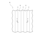
図1は、本実施形態のフレキシブルプリント配線板10の上面図である。図2は、AA線の模式的断面図である。図1と図2に示すように、本実施形態のフレキシブルプリント配線板10は、絶縁性を有するベースフィルム3と、ベースフィルム3の一方の表面に配置(積層)される複数本の配線13を有する配線層11とを主に備える。フレキシブルプリント配線板10は、ベースフィルム3又は配線層11の表面に絶縁膜(カバーフィルム)をさらに備えてもよい。この絶縁膜としては、例えば従来公知の樹脂フィルム等が挙げられ、この絶縁膜は、例えば接着剤によってベースフィルム3又は配線層11に接着される。[First embodiment]
[Flexible printed wiring board]
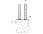
FIG. 1 is a top view of a flexible printed
<ベースフィルム>
ベースフィルム3は、絶縁性を有する合成樹脂製の層である。ベースフィルム3は、可撓性を有する。このベースフィルム3は、配線層11を形成するための基材でもある。ベースフィルム3の形成材料としては、絶縁性及び可撓性を有するものであれば特に限定されないが、シート状に形成された低誘電率の合成樹脂フィルムを採用し得る。この合成樹脂フィルムの主成分としては、例えばポリイミド、ポリエチレンテレフタレート、液晶ポリマー、フッ素樹脂等が挙げられる。「主成分」とは、最も含有量の多い成分であり、例えば形成材料中50質量%以上を占める成分を意味する。ベースフィルム3は、ポリイミド等の例示した樹脂以外の他の樹脂、帯電防止剤等を含有してもよい。<Base film>
The
ベースフィルム3の平均厚みの下限としては、特に限定されないが、3μmであってもよく、5μmであってもよく、10μmであってもよい。ベースフィルム3の平均厚みの上限としては、特に限定されないが、200μmであってもよく、150μmであってもよく、100μmであってもよい。ベースフィルム3の平均厚みが3μm未満である場合、ベースフィルム3の絶縁強度及び機械的強度が不十分となるおそれがある。一方、ベースフィルム3の平均厚みが200μmを超える場合、フレキシブルプリント配線板10が不要に厚くなるおそれがある。ここで、「平均厚み」とは、任意の十点において測定した厚みの平均値を意味する。なお、以下において他の部材等の「平均厚み」も、これと同様に測定される。
The lower limit of the average thickness of the
<配線層>
配線層11は、ベースフィルム3の表面に直接又は他の層を介して配置(積層)される。配線層11が有する配線13としては、例えば信号を送るための信号線、電力供給用の電流を送るための電流線、磁界発生用の電流を送るための電流線等が挙げられる。<Wiring layer>
The
配線13は、ベースフィルム3の表面に配置(積層)される第1導電性下地層23と、第1導電性下地層23におけるベースフィルム3とは反対の表面に配置(積層)される第1めっき層25と、第1導電性下地層23の両側面及び第1めっき層25の第1導電性下地層23とは反対の側の表面及び両側面を覆うように配置(積層)される第2めっき層27とによって形成される。
The
例えば配線13の横断面は、図2に示すように、配線13におけるベースフィルム3との接続部分からこの配線13の先端に向かう程、幅が大きくなるような形状である。換言すれば、横断面は、ベースフィルム3に向かう程先細りになっている形状である。すなわち、横断面は、逆台形状である。横断面が上記のように逆台形状であることで、配線13の両側面と絶縁膜との接着性をより大きくすることができる。よって、フレキシブルプリント配線板10が、より絶縁膜との接着性に優れる。図2のフレキシブルプリント配線板10において、第1めっき層25の側面に垂直方向の第2めっき層27の厚みが、ベースフィルムの表面と第2めっき層27との接触面から配線13の先端面に向けて大きくなる。
For example, as shown in FIG. 2, the cross section of the
配線13の平均線幅L1の下限としては、5μmであってもよく、7.5μmであってもよく、10μmであってもよい。配線13の平均線幅L1の上限としては、30μmであってもよく、25μmであってもよく、20μmであってもよい。配線13の平均線幅L1が5μmに満たない場合、配線13の製造が困難になるおそれがある。一方、配線13の平均線幅L1が30μmを超える場合、十分な配線密度を得られないおそれがある。「平均線幅」は、フレキシブルプリント配線板10の断面をミクロトーム等の断面加工装置で露出させ、各配線13における最も幅の大きい部分の長さを測定可能な顕微鏡等によって測定し、任意の十点の平均値として算出される値である。
The lower limit of the average line width L1 of the
互いに隣接して配置される複数の配線13の平均間隔S1の下限としては、1μmであり、さらに2μmであってもよい。配線13の平均間隔S1の上限としては、30μmであり、さらに20μmであってもよく、10μmであってもよい。配線13の平均間隔S1が1μmに満たない場合、短絡が発生するおそれがある。一方、配線13の平均間隔S1が30μmを超える場合、十分な配線密度を得られないおそれがある。「平均間隔」は、フレキシブルプリント配線板10の断面をミクロトーム等の断面加工装置で露出させ、各配線13間の隙間における最も間隔の小さい部分の長さを測定可能な顕微鏡等によって測定し、それらの平均値として算出される値である。
The lower limit of the average interval S1 between the plurality of
配線13の平均高さ(厚み)H1の下限としては、40μmであり、さらに50μmであってもよい。配線13の平均高さH1の上限としては、120μmであり、さらに100μmであってもよく、70μmであってもよく、60μmであってもよい。平均高さH1が40μmに満たない場合、機械的強度が不足するおそれがある。一方、平均高さH1が120μmを超える場合、後述するフレキシブルプリント配線板10の製造方法での配線13の形成が困難になるおそれがある。「平均高さ」は、フレキシブルプリント配線板10の断面をミクロトーム等の断面加工装置で露出させ、配線13において、任意の十点の断面観察による高さ(厚みに相当する。)を測定し、測定結果の平均値を算出することによって得られる。なお、以下において他の部材等の「平均高さ」も、これと同様に測定される。
The lower limit of the average height (thickness) H1 of the
第1導電性下地層23は、後述する導電性下地層M(例えば図3参照)の一部によって形成される。第1導電性下地層23の形成材料としては、例えば銅(Cu)、銀(Ag)、金(Au)、ニッケル(Ni)、チタン(Ti)、クロム(Cr)、これらの合金等が挙げられる。これら形成材料については、ベースフィルム3に対する配線層11の密着力の熱劣化を抑制する点で、第1導電性下地層23が、ベースフィルム3(例えばポリイミド)と接する側に、ニッケル、クロム、チタン及び銀よりなる群から選択される少なくとも1種を含有する層(第1層)を含んでもよい。さらに、第1導電性下地層23が、除去が容易で絶縁性を保つことが容易なニッケル及びクロムから選択される少なくとも1種を含有する層(第1層)を含んでもよい。また、第1導電性下地層23が、この第1層の上側(ベースフィルム3とは反対の側)に、銅を主成分とする層(第2層)を含んでもよい。この銅を主成分とする層が配置されることにより、電気めっきにより配線層11を形成する際に作業の短時間化が可能となる。
The first
例えば、第1層の平均厚みの下限としては、1nmであってもよく、2nmであってもよい。第1層の平均厚みの上限としては、15nmであってもよく、8nmであってもよい。平均厚みが1nmに満たない場合、ベースフィルム3に対する配線層11の密着力の熱劣化を抑制することが困難になるおそれがある。一方、平均厚みが15nmを超える場合、第1層が容易に除去され難くなり、配線層11の絶縁性を十分に保つことができないおそれがある。なお、この第1層は、スパッタ法、電気めっき法、無電解めっき法等によって形成され得る。
For example, the lower limit of the average thickness of the first layer may be 1 nm or 2 nm. The upper limit of the average thickness of the first layer may be 15 nm or 8 nm. If the average thickness is less than 1 nm, it may be difficult to suppress thermal deterioration of the adhesion of the
例えば、第2層の平均厚みの下限としては、0.1μmであってもよく、0.2μmであってもよい。第2層の平均厚みの上限としては、2μmであってもよく、1μmであってもよい。平均厚みが0.1μmに満たない場合、電気めっきによって配線層11を形成する時間が過度に長くなるおそれがある。一方、平均厚みが2μmを超える場合、第2層が容易に除去され難くなり、配線層11の絶縁性を十分に保つことができないおそれがある。なお、この第2層は、スパッタ法、電気めっき法、無電解めっき法等によって形成されることであってもよく、これらを組み合わせて形成されてもよい。特に、第1導電性下地層23の最上面側に無電解銅めっき層が配置されることであってもよく、これにより、それよりも内層がスパッタ法で形成された場合に、このスパッタ法によって生じ得る欠陥等をカバーすることができる。
For example, the lower limit of the average thickness of the second layer may be 0.1 μm or 0.2 μm. The upper limit of the average thickness of the second layer may be 2 μm or 1 μm. If the average thickness is less than 0.1 μm, it may take an excessively long time to form the
第1めっき層25を形成するための第1金属材料としては、例えば銅、ニッケル、金、銀、白金等を用いることができ、中でも比較的安価で導電性に優れる銅や比較的安価で耐食性に優れるニッケルが好適に用いられる。
As the first metal material for forming the
第1めっき層25は、後述するように、レジストパターンを用いて形成される。すなわち、第1めっき層25は、その長手方向に沿った2つの側面がレジストパターンに接触しつつ形成される。
The
第2めっき層27を形成するための第2金属材料としては、第1金属材料と同様、例えば銅、ニッケル、金、銀、白金等を用いることができ、中でも比較的安価で導電性に優れる銅や比較的安価で耐食性に優れるニッケルが好適に用いられる。
As the second metal material for forming the
第2めっき層27は、後述するように、レジストパターンを用いることなく形成される。
The
本実施形態では、第2めっき層27における長手方向に沿った先端面27aが、配線13における長手方向に沿った先端面に相当し、第2めっき層27における長手方向に沿った2つの側面27b及び27c(図2の左右の側面)が、配線13における長手方向に沿った2つの側面に相当する。本実施形態では、これら2つの側面27b、27cの算術平均粗さRaが0.05以上2.0以下である。
In this embodiment, the
各側面27b、27cの算術平均粗さRaの下限としては、上記の通り、それぞれ0.05であり、さらに0.1であってもよい。各側面27b、27cの算術平均粗さRaの上限としては、上記の通り、それぞれ2.0であり、さらに1.0であってもよく、0.7であってもよい。Raが0.05に満たない場合、絶縁膜との接着性が劣るおそれがある。一方、Raが2.0を超える場合、高周波特性が悪化するおそれがある。加えて、Raが2.0を超える場合、隣接する配線13間に短絡が生じるおそれがある。Raは、後述する実施例に記載の方法によって測定される。
As described above, the lower limit of the arithmetic mean roughness Ra of each of the side surfaces 27b and 27c is 0.05, and may be 0.1. As described above, the upper limit of the arithmetic mean roughness Ra of each of the side surfaces 27b and 27c is 2.0, and may be 1.0 or 0.7. If Ra is less than 0.05, the adhesiveness to the insulating film may deteriorate. On the other hand, if Ra exceeds 2.0, the high frequency characteristics may deteriorate. In addition, if Ra exceeds 2.0, a short circuit may occur between
配線13の先端面27aの算術平均粗さRaは特に限定されない。例えば先端面27aの算術平均粗さRaの下限としては0.05であってもよく、0.1であってもよい。先端面27aのRaの上限としては、2.0であってもよく、1.0であってもよく、0.7であってもよい。Raが0.05に満たない場合、絶縁膜との接着性を十分に高められないおそれがある。一方、Raが2.0を超える場合、高周波特性が悪化するおそれがある。先端面27aの算術平均粗さRaは、測定対象を側面から先端面に変更し、特にベースフィルムを切断することなく、後述する実施例に記載の側面のRaの測定方法と同様にして測定される。
The arithmetic average roughness Ra of the
2つの側面27b、27c、及び先端面27aの算術平均粗さRaは、後述するように、第2めっき液中の添加剤、及び電流密度を調整することによって、調整することができる。
The arithmetic mean roughness Ra of the two
<利点>
フレキシブルプリント配線板10は、配線13の平均高さH1及び平均間隔S1が上記範囲であり、側面27b、27cの算術平均粗さRaが上記範囲内であることで、短絡を抑制することができる。加えて、配線13を覆うように絶縁膜が積層される場合、この絶縁膜と配線13との接着性を大きくすることができる。従って、フレキシブルプリント配線板10は、絶縁膜との接着性に優れ、しかも短絡が抑制されている。<Advantages>
In the flexible printed
[第二実施形態]
〔フレキシブルプリント配線板の製造方法〕
次に、第一実施形態に係るフレキシブルプリント配線板の製造方法について説明する。[Second embodiment]
[Method for manufacturing flexible printed wiring board]
Next, a method for manufacturing a flexible printed wiring board according to the first embodiment will be described.
フレキシブルプリント配線板10の製造方法は、表面に導電性下地層Mが積層されたベースフィルム3を準備し、レジストパターンR1を用い、第1めっき液中にてベースフィルム3上の導電性下地層M上に電気めっきすることにより、第1めっき層25を形成する第1めっき工程と、レジストパターンR1及び導電性下地層Mにおける第1めっき層25の非積層領域を除去する第1除去工程(除去する工程)と、第1除去する工程の後、第2めっき液中にて第1めっき層25に電気めっきすることにより、第2めっき層27を形成する第2めっき工程とを備える。本実施形態では、第2めっき液が、2500以上8000以下の数平均分子量を有するポリエチレングリコールを含有する。第2めっき工程では、配線13の側面(ここでは第2めっき層27の2つの側面27b、27c)の算術平均粗さRaが0.05以上2.0以下となるように電気めっきの電流密度を調整する。
The method for manufacturing the flexible printed
<導電性下地層>
導電性下地層Mは、ベースフィルム3の表面に積層される。この導電性下地層Mは、予めベースフィルム3の表面の全面に積層されたものを用いる。導電性下地層Mの一部が、第1導電性下地層23となる。<Conductive underlayer>
A conductive underlayer M is laminated on the surface of the
導電性下地層Mの形成材料としては、例えば銅(Cu)、銀(Ag)、金(Au)、ニッケル(Ni)、チタン(Ti)、クロム(Cr)、これらの合金等が挙げられる。これら形成材料については、ベースフィルム3に対する配線層11の密着力の熱劣化を抑制する点で、導電性下地層Mが、ベースフィルム3(例えばポリイミド)と接する側に、ニッケル、クロム、チタン及び銀よりなる群から選択される少なくとも1種を含有する層(第1層)を含んでもよい。さらに、導電性下地層Mが、除去が容易で絶縁性を保つことが容易なニッケル及びクロムから選択される少なくとも1種を含有する層(第1層)を含んでもよい。また、導電性下地層Mが、この第1層の上側(ベースフィルム3とは反対の側)に、銅を主成分とする層(第2層)を含んでもよい。この銅を主成分とする層が配置されることにより、電気めっきにより配線層11を形成する際に作業の短時間化が可能となる。
Materials for forming the conductive underlayer M include, for example, copper (Cu), silver (Ag), gold (Au), nickel (Ni), titanium (Ti), chromium (Cr), and alloys thereof. Regarding these forming materials, nickel, chromium, titanium, and nickel, chromium, titanium, and the like are added to the side of the conductive underlying layer M in contact with the base film 3 (for example, polyimide) in order to suppress thermal deterioration of the adhesion of the
例えば、第1層の平均厚みの下限としては、1nmであってもよく、2nmであってもよい。第1層の平均厚みの上限としては、15nmであってもよく、8nmであってもよい。平均厚みが1nmに満たない場合、ベースフィルム3に対する配線層11の密着力の熱劣化を抑制することが困難になるおそれがある。一方、平均厚みが15nmを超える場合、第1層が容易に除去され難くなり、配線層11の絶縁性を十分に保つことができないおそれがある。なお、この第1層は、スパッタ法、電気めっき法、無電解めっき法等によって形成され得る。
For example, the lower limit of the average thickness of the first layer may be 1 nm or 2 nm. The upper limit of the average thickness of the first layer may be 15 nm or 8 nm. If the average thickness is less than 1 nm, it may be difficult to suppress thermal deterioration of the adhesion of the
例えば、第2層の平均厚みの下限としては、0.1μmであってもよく、0.2μmであってもよい。第2層の平均厚みの上限としては、2μmであってもよく、1μmであってもよい。平均厚みが0.1μmに満たない場合、電気めっきによって配線層11を形成する時間が過度に長くなるおそれがある。一方、平均厚みが2μmを超える場合、第2層が容易に除去され難くなり、配線層11の絶縁性を十分に保つことができないおそれがある。なお、この第2層は、スパッタ法、電気めっき法、無電解めっき法等によって形成されてもよく、これらを組み合わせて形成されてもよい。特に、導電性下地層Mの最上面側に無電解銅めっき層が配置されてもよく、これにより、それよりも内層がスパッタ法で形成された場合に、このスパッタ法によって生じ得る欠陥等をカバーすることができる。
For example, the lower limit of the average thickness of the second layer may be 0.1 μm or 0.2 μm. The upper limit of the average thickness of the second layer may be 2 μm or 1 μm. If the average thickness is less than 0.1 μm, it may take an excessively long time to form the
<第1めっき工程>
本工程は、導電性下地層Mの表面にフォトレジスト膜を積層する工程と、このフォトレジスト膜への露光及び現像により第1めっき層25の反転形状のレジストパターンを形成する工程と、このレジストパターンの開口部の導電性下地層M上への電気めっきにより第1めっき層25を形成する工程とを備える。<First plating step>
This step includes a step of laminating a photoresist film on the surface of the conductive base layer M, a step of forming a resist pattern of the inverted shape of the
(フォトレジスト膜を積層する工程)
フォトレジスト膜を積層する工程では、導電性下地層Mの表面にフォトレジスト膜(不図示)を積層する。(Step of laminating a photoresist film)
In the step of laminating a photoresist film, a photoresist film (not shown) is laminated on the surface of the conductive underlying layer M. As shown in FIG.
フォトレジスト膜は、感光することにより高分子の結合が強化されて現像液に対する溶解性が低下するネガ型レジスト組成物、又は感光することにより高分子の結合が弱化されて現像液に対する溶解性が増大するポジ型レジスト組成物によって形成される。 The photoresist film is a negative resist composition in which the polymer bond is strengthened by exposure to light and the solubility in the developer is reduced, or the polymer bond is weakened by the exposure to light and the solubility in the developer is reduced. formed by increasing positive resist compositions.
フォトレジスト膜は、液状のレジスト組成物の塗工及び乾燥によって導電性下地層M上に形成してもよいが、室温で流動性を有しないドライフィルムフォトレジストを熱圧着により積層してもよい。フォトレジスト膜としてドライフィルムフォトレジストを用いることによって、フォトレジスト膜の厚みを均一かつ小さくすることができるので、レジストパターンの細密化が容易となる。 The photoresist film may be formed on the conductive underlayer M by coating and drying a liquid resist composition, but a dry film photoresist that does not have fluidity at room temperature may be laminated by thermocompression bonding. . By using a dry film photoresist as the photoresist film, the thickness of the photoresist film can be made uniform and small, so that the resist pattern can be easily miniaturized.
フォトレジスト膜の平均高さ(厚さ)の下限としては、45μmであってもよく、50μmであってもよい。一方、フォトレジスト膜の平均高さの上限としては、170μmであってもよく、150μmであってもよい。フォトレジスト膜の平均高さが45μmに満たない場合、ドライフィルムレジストの取り扱いが容易でなくなるおそれがある。一方、フォトレジスト膜の平均高さが170μmを超える場合、レジストパターンの形状の精度が低下するおそれがある。 The lower limit of the average height (thickness) of the photoresist film may be 45 μm or 50 μm. On the other hand, the upper limit of the average height of the photoresist film may be 170 μm or 150 μm. If the average height of the photoresist film is less than 45 μm, handling of the dry film resist may not be easy. On the other hand, if the average height of the photoresist film exceeds 170 μm, the shape accuracy of the resist pattern may deteriorate.
(レジストパターンを形成する工程)
レジストパターンを形成する工程では、先ず例えばフォトマスク等を用いてフォトレジスト膜を選択的に露光することにより、フォトレジスト膜に現像液に溶解する部分と溶解しない部分とを形成する。(Step of forming a resist pattern)
In the step of forming the resist pattern, first, the photoresist film is selectively exposed using, for example, a photomask or the like to form a portion that dissolves in the developer and a portion that does not dissolve in the photoresist film.
続いて、現像液を用いてフォトレジスト膜の溶解性の高い部分を洗い流すことで、図3に示すように形成すべき第1めっき層25に対応する部分が開口部とされたレジストパターンR1を得る。
Subsequently, by washing away the highly soluble portion of the photoresist film using a developer, a resist pattern R1 having openings corresponding to the
レジストパターンR1は、第1めっき層25を画定する複数の開口部を有する。この開口部の平均幅の下限としては、5μmであってもよく、10μmであってもよく、15μmであってもよい。一方、開口部の平均幅の上限としては、50μmであってもよく、40μmであってもよく、30μmであってもよい。開口部の平均幅が5μmより小さいと、開口部の幅のバラツキが大きくなるおそれがあるほか、第2めっき層27の高さ(2次めっき量)が大きくなり過ぎて、寸法のバラツキ及びフレキシブルプリント配線板の製造コストが増大するおそれがある。逆に、開口部の平均幅が50μmを超えると、レジストパターンR1が剥離し易くなるおそれがあるほか、配線密度が要求を満たせないおそれがある。なお、レジストパターンR1の第1めっき層25に対応する開口部の平均幅は、後述する第1除去工程でのエッチング前の第1めっき層25の平均幅と同等である。
Resist pattern R1 has a plurality of openings that define
(第1めっき層を形成する工程)
第1めっき層を形成する工程では、第1めっき液を用い、レジストパターンR1の開口部内に露出する導電性下地層Mに電気めっきによって金属を積層することで、図4に示すように、第1めっき層25を形成する。(Step of forming first plating layer)
In the step of forming the first plating layer, a first plating solution is used to deposit a metal on the conductive base layer M exposed in the opening of the resist pattern R1 by electroplating, thereby forming a first plating layer as shown in FIG. 1
具体的には、この第1めっき層を形成する工程では、ベースフィルム3、導電性下地層M及びレジストパターンR1の積層体とこの積層体に対向する電極とを第1めっき液中に配置し、直流電源の負極を導電性下地層Mに接続し、正極を対向電極に接続することで、第1めっき液中の金属を導電性下地層M表面に析出させる。
Specifically, in the step of forming the first plating layer, the laminate of the
電気めっきにより積層する金属、すなわち第1めっき層25を形成するための第1金属材料としては、上述したように、例えば銅、ニッケル、金、銀、白金等を用いることができ、中でも比較的安価で導電性に優れる銅や比較的安価で耐食性に優れるニッケルが好適に用いられる。
As the metal to be laminated by electroplating, that is, the first metal material for forming the
第1めっき液としては、第1金属材料と、第1添加剤とを含有するものが挙げられる。第1添加剤としては、後述するポリエチレングリコールの他、硫酸銅五水和物、硫酸、塩素イオン(塩化物イオン)、3,3’-ジチオビス(1-プロパンスルホン酸)2ナトリウム(SPS)等が挙げられる。第1めっき液として、後述する第2めっき液と同じものを用いることができる。 Examples of the first plating solution include those containing a first metal material and a first additive. As the first additive, in addition to polyethylene glycol described later, copper sulfate pentahydrate, sulfuric acid, chloride ion (chloride ion), 3,3′-dithiobis(1-propanesulfonic acid) disodium (SPS), etc. is mentioned. As the first plating solution, the same one as the second plating solution described later can be used.
第1めっき層を形成する工程で形成されるエッチング前の第1めっき層25の平均高さの下限としては、20μmであってもよく、25μmであってもよく、30μmであってもよい。
一方、エッチング前の第1めっき層25の平均高さの上限としては、125μmであってもよく、120μmであってもよく、118μmであってもよい。エッチング前の第1めっき層25の平均高さが20μmより小さいと、第2めっき層27の高さ(2次めっき量)が大きくなり過ぎて、寸法のバラツキ及びフレキシブルプリント配線板の製造コストが増大するおそれがある。逆に、エッチング前の第1めっき層25の平均高さが125μmを超えると、レジストパターンR1が剥離しにくくなるおそれや、フレキシブルプリント配線板10が不要に厚くなるおそれがある。The lower limit of the average height of the
On the other hand, the upper limit of the average height of the
<第1除去工程>
第1除去工程では、図5に示すように第1めっき層25形成後にレジストパターンR1及びその底部の導電性下地層Mを除去する。<First removal step>
In the first removing step, as shown in FIG. 5, after forming the
レジストパターンR1の除去は、レジストパターンR1を導電性下地層Mから剥離することで行われる。具体的には、レジストパターンR1、第1めっき層25、導電性下地層M及びベースフィルム3を有する積層体を剥離液に浸漬させることで、レジストパターンR1を剥離液により膨張させる。これにより、レジストパターンR1と導電性下地層Mとの間に反発力が生じ、レジストパターンR1が導電性下地層Mから剥離する。この剥離液としては公知のものを用いることができる。
The removal of the resist pattern R1 is performed by peeling the resist pattern R1 from the conductive underlying layer M. As shown in FIG. Specifically, the laminate having the resist pattern R1, the
レジストパターンR1底部の導電性下地層Mの除去は、レジストパターンR1剥離後に露出する導電性下地層Mを、第1めっき層25がマスクの役目を果たしエッチングにより除去する。これにより、複数の第1めっき層25が電気的に分離される。このエッチングには導電性下地層Mを形成する金属を浸食するエッチング液が使用される。
The removal of the conductive base layer M at the bottom of the resist pattern R1 is performed by etching the conductive base layer M exposed after the resist pattern R1 is peeled off, using the
エッチング量は、導電性下地層Mが完全に除去される量であればよいが、フレキシブルプリント配線板10の製造方法では、第1めっき層25の平均エッチング量を0.5μm以上3.0μm未満であってもよい。また、平均エッチング量を2.0μm以下であってもよい。なお、「第1めっき層の平均エッチング量」とは、配線の長手方向と垂直な断面におけるエッチング前の第1めっき層の面積とエッチング後の第1めっき層の面積との差をエッチング前の第1めっき層の外面(ベースフィルムとの積層面は除く)の長さで除して得られる厚みを配線の長手方向に平均した値である。
The etching amount may be an amount that completely removes the conductive base layer M. In the method for manufacturing the flexible printed
<第2めっき工程>
第2めっき工程では、第2めっき液を用い、第1めっき層25の表面に電気めっきにより第2めっき層27を被覆し、配線13を形成する。この電気めっきは例えば公知の電気めっき法を用い、後述するように電流密度を調整することにより行うことができる。これにより、上述したような図2のフレキシブルプリント配線板10が得られる。実施形態の製造方法においては、このように、いわゆるセミアディティブ法が好適に用いられる。<Second plating process>
In the second plating step, a second plating solution is used to electroplat the surface of the
電気めっきにより積層する金属、すなわち第2めっき層27を形成するための第2金属材料としては、上述したように、例えば銅、ニッケル、金、銀、白金等を用いることができ、中でも比較的安価で導電性に優れる銅や比較的安価で耐食性に優れるニッケルが好適に用いられる。
As the metal laminated by electroplating, that is, the second metal material for forming the
この電気めっきにおいて用いる第2めっき液は、2500以上8000以下の数平均分子量を有するポリエチレングリコール(PEG)を含有する。この第2めっき液としては、第2金属材料と、第2添加剤としてポリエチレングリコールとを含有するものが挙げられる。ポリエチレングリコール以外の第2添加剤としては、上述した第1添加剤と同様、硫酸銅五水和物、硫酸、塩素イオン(塩化物イオン)、3,3’-ジチオビス(1-プロパンスルホン酸)2ナトリウム(SPS)等が挙げられる。 The second plating solution used in this electroplating contains polyethylene glycol (PEG) having a number average molecular weight of 2500 or more and 8000 or less. Examples of the second plating solution include those containing a second metal material and polyethylene glycol as a second additive. As the second additive other than polyethylene glycol, copper sulfate pentahydrate, sulfuric acid, chloride ion (chloride ion), 3,3′-dithiobis(1-propanesulfonic acid), as in the first additive described above. disodium (SPS) and the like.
ポリエチレングリコールの数平均分子量Mnの下限としては、2500であり、さらに2700であってもよく、3000であってもよい。数平均分子量Mnの上限としては、8000であり、さらに7000であってもよく、5000であってもよい。数平均分子量Mnが2500に満たない場合、第2めっき層27の2つの側面27b、27c、及び先端面27aの算術平均粗さRaを上記範囲内に設定することが困難になるおそれがある。一方、数平均分子量Mnが8000を超える場合にも、第2めっき層27の2つの側面27b、27c、及び先端面27aの算術平均粗さRaを上記範囲内に設定することが困難になるおそれがある。
The lower limit of the number average molecular weight Mn of polyethylene glycol is 2,500, and may be 2,700 or 3,000. The upper limit of the number average molecular weight Mn is 8,000, and may be 7,000 or 5,000. If the number average molecular weight Mn is less than 2500, it may be difficult to set the arithmetic average roughness Ra of the two
例えばポリエチレングリコールの重量平均分子量Mwの下限としては、10000であってもよく、10100であってもよい。重量平均分子量Mwの上限としては、20000であってもよく、18000であってもよく、16000であってもよく、15000であってもよい。重量平均分子量Mwが10000に満たない場合、第2めっき層27の2つの側面27b、27c、及び先端面27aの算術平均粗さRaを上記範囲内に設定することが困難になるおそれがある。一方、重量平均分子量Mwが20000を超える場合にも、第2めっき層27の2つの側面27b、27c、及び先端面27aの算術平均粗さRaを上記範囲内に設定することが困難になるおそれがある。
For example, the lower limit of the weight average molecular weight Mw of polyethylene glycol may be 10,000 or 10,100. The upper limit of the weight average molecular weight Mw may be 20,000, 18,000, 16,000, or 15,000. If the weight average molecular weight Mw is less than 10000, it may be difficult to set the arithmetic average roughness Ra of the two
例えばポリエチレングリコールのz平均分子量Mzの下限としては、15000であってもよく、16000であってもよい。z平均分子量Mzの上限としては、25000であってもよく、22000であってもよく、20000であってもよい。z平均分子量Mzが15000に満たない場合、第2めっき層27の2つの側面27b、27c、及び先端面27aの算術平均粗さRaを上記範囲内に設定することが困難になるおそれがある。一方、z平均分子量Mzが25000を超える場合にも、第2めっき層27の2つの側面27b、27c、及び先端面27aの算術平均粗さRaを上記範囲内に設定することが困難になるおそれがある。
For example, the lower limit of the z-average molecular weight Mz of polyethylene glycol may be 15,000 or 16,000. The upper limit of the z-average molecular weight Mz may be 25,000, 22,000, or 20,000. If the z-average molecular weight Mz is less than 15,000, it may be difficult to set the arithmetic average roughness Ra of the two
第2めっき工程での電流密度は、特に限定されず、適宜設定され得る。例えば電流密度の下限としては、合計で0.3A/m2であってもよく、0.5A/m2であってもよく、1A/m2であってもよい。電流密度の上限としては、合計で5A/m2であってもよく、4A/m2であってもよく、3A/m2であってもよい。電流密度が0.3A/m2に満たない場合、第2めっき層27の2つの側面27b、27c、及び先端面27aの算術平均粗さRaを上記範囲内に設定することが困難になるおそれがある。一方、電流密度が5A/m2を超える場合にも、第2めっき層27の2つの側面27b、27c、及び先端面27aの算術平均粗さRaを上記範囲内に設定することが困難になるおそれがある。The current density in the second plating step is not particularly limited and can be set as appropriate. For example, the lower limit of current density may be 0.3 A/m 2 in total, 0.5 A/m 2 , or 1 A/m 2 . The upper limit of the current density may be 5 A/m 2 in total, 4 A/m 2 or 3 A/m 2 . If the current density is less than 0.3 A/m 2 , it may be difficult to set the arithmetic average roughness Ra of the two
第2めっき工程では、電流密度を1段階で調整してもよく、2段階で調整してもよい。このように、第2めっき工程において電流密度を2段階で調整することで、算術平均粗さRaを上記範囲内に調整することが容易になる。電流密度を1段階で調整する場合、電流密度の下限及び上限としては、上記の範囲であってもよい。 In the second plating step, the current density may be adjusted in one step or in two steps. Thus, by adjusting the current density in two steps in the second plating step, it becomes easy to adjust the arithmetic mean roughness Ra within the above range. When the current density is adjusted in one step, the lower and upper limits of the current density may be within the above ranges.
電流密度を2段階で調整する場合、2段階目の電流密度が1段階目の電流密度よりも大きくてもよい。この場合において、例えば1段階目の電流密度の下限としては、0.1A/m2であってもよく、0.3A/m2であってもよい。1段階目の電流密度の上限としては、1.5A/m2であってもよく、1.0A/m2であってもよい。2段階目の電流密度の下限としては、0.2A/m2であってもよく、1.0A/m2であってもよい。2段階目の電流密度の上限としては、5A/m2であってもよく、3A/m2であってもよい。When adjusting the current density in two stages, the current density in the second stage may be higher than the current density in the first stage. In this case, for example, the lower limit of the current density in the first stage may be 0.1 A/m 2 or 0.3 A/m 2 . The upper limit of the current density in the first stage may be 1.5 A/m 2 or 1.0 A/m 2 . The lower limit of the second stage current density may be 0.2 A/m 2 or 1.0 A/m 2 . The upper limit of the second stage current density may be 5 A/m 2 or 3 A/m 2 .
<利点>
フレキシブルプリント配線板10の製造方法によれば、絶縁膜との接着性に優れ、しかも短絡が抑制されたフレキシブルプリント配線板10を製造することができる。フレキシブルプリント配線板10の製造方法によると、比較的密な配線パターン(配線の平均高さが40μm以上120μm以下、配線の平均間隔が1μm以上30μm以下)であっても、配線の側面を所定の表面粗さに調整することが可能となる。<Advantages>
According to the manufacturing method of the flexible printed
[第三実施形態]
〔フレキシブルプリント配線板〕
図6に示すように、本実施形態のフレキシブルプリント配線板30は、絶縁性を有するベースフィルム3と、ベースフィルム3の一方の表面に配置(積層)される複数の配線33を有する配線層31とを主に備える。上述した第一実施形態と同様、フレキシブルプリント配線板30は、ベースフィルム3又は配線層31の表面に絶縁膜(カバーフィルム)をさらに備えてもよい。[Third Embodiment]
[Flexible printed wiring board]
As shown in FIG. 6, a flexible printed
本実施形態のフレキシブルプリント配線板30では、配線33が、第2導電性下地層43と、第2導電性下地層43上に配置された1層の第3めっき層45とを有する。
In the flexible printed
<ベースフィルム>
本実施形態のベースフィルム3は、第一実施形態のベースフィルム3と同じであるため、その詳細な説明を省略する。<Base film>
Since the
<配線層>
配線層31は、ベースフィルム3の表面に直接又は他の層を介して配置(積層)される。配線層31が有する配線33としては、上述した第一実施形態と同様、例えば信号を送るための信号線、電力供給用の電流を送るための電流線、磁界発生用の電流を送るための電流線等が挙げられる。<Wiring layer>
The
配線33は、ベースフィルム3の表面に配置(積層)される第2導電性下地層43と、第2導電性下地層43のベースフィルム3と反対の側の表面に配置(積層)される第3めっき層45とによって形成される。
The
配線33の平均線幅L2、平均間隔S2及び平均高さH2は、第一実施形態の配線13と同様に設定され得る。
The average line width L2, average spacing S2, and average height H2 of the
第2導電性下地層43の形成材料としては、第一実施形態の第1導電性下地層23と同じものが使用され得る。
As the material for forming the second
第3めっき層45を形成するための第3金属材料としては、第一実施形態の第1めっき層25及び第2めっき層27を形成するための第1金属材料及び第2金属材料と同じものが使用され得る。
The third metal material for forming the
本実施形態では、第2導電性下地層43における長手方向に沿った2つの側面(図6の左右の側面)43b、43c、及び第3めっき層45における長手方向に沿った2つの側面(図6の左右の側面)45b、45cが、配線33における長手方向に沿った2つの側面に相当する。第3めっき層45における長手方向に沿った先端面45aが、配線33における長手方向に沿った先端面に相当する。
In this embodiment, the second
本実施形態では、上述した第一実施形態と同様、配線33の2つの側面の算術平均粗さRaが0.05以上2.0以下である。
In this embodiment, the arithmetic average roughness Ra of the two side surfaces of the
配線33の側面の算術平均粗さRaの下限としては、上述した第一実施形態と同様、0.05であり、さらに0.1であってもよい。側面のRaの上限としては、第一実施形態と同様、2.0であり、さらに1.0であってもよく、0.7であってもよい。
The lower limit of the arithmetic mean roughness Ra of the side surface of the
配線33の先端面(ここでは第3めっき層45の先端面45a)の算術平均粗さRaの下限としては、上述した第一実施形態と同様、0.05であってもよく、1.0であってもよい。先端面のRaの上限としては、上述した第一実施形態と同様、2.0であってもよく、1.0であってもよく、0.7であってもよい。
The lower limit of the arithmetic mean roughness Ra of the tip surface of the wiring 33 (here, the
配線33の2つの側面の該当部分、及び先端面の算術平均粗さRaは、後述するように、エッチング条件を調整することによって、調整することができる。
The corresponding portions of the two side surfaces of the
〔フレキシブルプリント配線板の製造方法〕
次に、第三実施形態に係るフレキシブルプリント配線板30の製造方法について説明する。[Method for manufacturing flexible printed wiring board]
Next, a method for manufacturing the flexible printed
フレキシブルプリント配線板30の製造方法は、レジストパターンR2(不図示)を用い、第3めっき液中にて一方の表面に導電性下地層Mが積層されたベースフィルム3の導電性下地層M上に電気めっきすることにより、第3めっき層45を形成する第3めっき工程と、レジストパターンR2及び導電性下地層Mにおける第3めっき層45の非積層領域を除去する第2除去工程と、第2除去工程の後、第3めっき層45の表面の算術平均粗さRaを調整する表面粗さ調整工程とを備える。表面粗さ調整工程では、第3めっき層45の側面のRaが0.05以上2.0以下となるように第3めっき層45の表面粗さを調整する。
The manufacturing method of the flexible printed
本実施形態では配線33の各側面のRaが0.05以上2.0以下となるように第3めっき層45及び第2導電性下地層43の表面粗さを調整する。
In this embodiment, the surface roughness of the
本実施形態では配線33の先端面(すなわち、第3めっき層45の先端面45a)のRaが0.05以上2.0以下となるように第3めっき層45の表面粗さを調整する。
In the present embodiment, the surface roughness of the
<導電性下地層>
導電性下地層Mとしては、上述した第二実施形態と同じのものを用いる。この導電性下地層Mの一部が、第2導電性下地層43となる。<Conductive underlayer>
As the conductive base layer M, the same one as in the above-described second embodiment is used. A portion of this conductive base layer M becomes the second
<第3めっき工程>
本工程は、第二実施形態の第1めっき工程と同様の工程を行う。本工程により、導電性下地層MにおけるレジストパターンR2(不図示)の開口部に第3めっき層45が積層された積層体が得られる。<Third Plating Process>
This step is the same step as the first plating step of the second embodiment. Through this step, a laminate in which the
<第2除去工程>
第2除去工程では、上述した第二実施形態の第1除去工程と同様の工程を行う。本工程により、レジストパターンR2及びその底部の導電性下地層Mを除去する。<Second removal step>
In the second removing process, the same process as the first removing process of the second embodiment described above is performed. In this step, the resist pattern R2 and the conductive base layer M on the bottom thereof are removed.
<表面粗さ調整工程>
本工程では、第2導電性下地層43の両側面43b、43c及び第3めっき層45の両側面45b、45c及び先端面45aをエッチングすることにより、これらの表面粗さを調整する。このエッチングには硫酸過酸化水素等のエッチング液が使用される。本工程により、配線33の長手方向に沿った両側面の算術平均粗さRaが上記範囲内に調整される。これと共に、配線33の先端面の算術平均表面粗さRaが上記範囲内に調整される。<Surface roughness adjustment process>
In this step, both side surfaces 43b and 43c of the second
なお、表面粗さ調整工程を、第2除去工程での導電性下地層Mのエッチングと同時に行ってもよい。 Note that the surface roughness adjustment step may be performed simultaneously with the etching of the conductive base layer M in the second removal step.
<利点>
フレキシブルプリント配線板30は、配線33の平均高さH2及び平均間隔S2が上記範囲であり、側面の算術平均粗さRaが上記範囲内であることで、短絡を抑制することができる。加えて、配線33を覆うように絶縁膜が積層される場合、この絶縁膜と配線33との接着性を大きくすることができる。従って、フレキシブルプリント配線板30は、絶縁膜との接着性に優れ、しかも短絡が抑制されている。<Advantages>
In the flexible printed
[その他の実施形態]
実施形態では、単一のベースフィルムと、このベースフィルムの一方の表面に積層された配線層を有するフレキシブルプリント配線板について説明したが、フレキシブルプリント配線板10は、単一のベースフィルムの両方の表面に配線層が積層されたものであってもよい。また、フレキシブルプリント配線板10は、複数のベースフィルムを有し、各ベースフィルムが一方の表面又は両方の表面に複数の配線層を有する多層プリント配線板であってもよい。この場合、ランド部を介して両面の配線層が導通され得る。[Other embodiments]
In the embodiments, a flexible printed wiring board having a single base film and a wiring layer laminated on one surface of this base film has been described, but the flexible printed
実施形態では、ベースフィルムに1の配線層が積層される場合について説明したが、ベースフィルムに複数の配線層が互いに間隔を空けて積層されてもよい。 In the embodiment, the case where one wiring layer is laminated on the base film has been described, but a plurality of wiring layers may be laminated on the base film at intervals.
実施形態では、各配線層11、31が各配線13、33を有する場合について説明したが、各配線層11、31がこれら配線13、33以外の配線を有する態様も採用し得る。
Although the wiring layers 11 and 31 have the
今回開示された実施の形態は全ての点で例示であって制限的なものではないと考えられるべきである。本発明の範囲は、上記実施形態の構成に限定されるものではなく、請求の範囲によって示され、請求の範囲と均等の意味及び範囲内での全ての変更が含まれることが意図される。 It should be considered that the embodiments disclosed this time are illustrative in all respects and not restrictive. The scope of the present invention is not limited to the configurations of the above-described embodiments, but is indicated by the scope of the claims, and is intended to include all modifications within the scope and meaning equivalent to the scope of the claims.
<試料の作製>
(参考例1、2、比較例1、2、実験例1~4)
ベースフィルムの一面側(表面側)に導電性下地層が積層されたフィルム(ユーピレックス(登録商標)-S、宇部興産社製)を用い、上述した第二実施形態と同様の製造方法により、図2に示すような配線板、すなわちフィルムの導電性下地層に第1めっき層及び第2めっき層が積層された複数の配線を有する配線層を備える配線板を作製した。具体的には、以下のようにして配線板を作製した。<Preparation of sample>
(Reference Examples 1 and 2, Comparative Examples 1 and 2, Experimental Examples 1 to 4)
Using a film (Upilex (registered trademark)-S, manufactured by Ube Industries, Ltd.) in which a conductive underlayer is laminated on one side (surface side) of the base film, a manufacturing method similar to that of the second embodiment described above is used. 2, that is, a wiring board provided with a wiring layer having a plurality of wirings in which a first plating layer and a second plating layer are laminated on a conductive base layer of a film. Specifically, a wiring board was produced as follows.
(めっき液)
下記の組成のめっき液を用い、PEGの種類を表1に示すように変更した。表1に示すPEGの各分子量は、下記の方法で測定した。
硫酸銅五水和物:75g/L
硫酸:190g/L
塩酸(塩化物イオンの供給源):55mg/L
PEG:0.02mmol/L
3,3’-ジチオビス(1-プロパンスルホン酸)2ナトリウム(SPS):0.5mmol/L
ヤヌスグリーンB(JGB):0.05mmol(Plating solution)
A plating solution having the following composition was used, and the type of PEG was changed as shown in Table 1. Each molecular weight of PEG shown in Table 1 was measured by the following method.
Copper sulfate pentahydrate: 75g/L
Sulfuric acid: 190g/L
Hydrochloric acid (source of chloride ions): 55 mg/L
PEG: 0.02mmol/L
3,3′-Dithiobis(1-propanesulfonic acid) disodium (SPS): 0.5 mmol/L
Janus Green B (JGB): 0.05 mmol
(PEGの数平均分子量Mn、重量平均分子量Mw及びz平均分子量Mzの測定)
PEGの数平均分子量Mn、重量平均分子量Mw及びz平均分子量MzをGPC法(gel permeation chromatography)で測定した。試料であるPEG原液を中和した後(塩が析出)、遠心分離を行い、得られた上澄み液を回収後、フィルターを用いてろ過を行い、試料溶液を調整した。測定条件を下記に示す。下記のゲル浸透クロマトグラフGPC装置を用い、下記の検出器及びカラムを準備し、下記の硝酸ナトリウム水溶液を溶媒とし、下記の流速に設定し、下記の注入量で試料溶液を注入した。
カラム温度は下記のように設定した。
・測定条件
装置:ゲル浸透クロマトグラフGPC(機器No.GPC-28)
検出器:示差屈折率検出器RI(昭和電工社製RI-201、感度:32)
カラム:TSKgel G3000PWXL 2本(7.8mm×30cm、東ソー社製)
溶媒:0.1M硝酸ナトリウム水溶液
流速:0.7mL/min
カラム温度:23℃
注入量:0.2mL
標準試料:東ソー社、Agilent社及びSigma Aldrich社製の単分散ポリエチレンオキサイド(PEO)及びポリエチレングリコール(PEG)(Measurement of number average molecular weight Mn, weight average molecular weight Mw and z average molecular weight Mz of PEG)
The number average molecular weight Mn, weight average molecular weight Mw and z average molecular weight Mz of PEG were measured by GPC (gel permeation chromatography). After neutralizing the PEG undiluted solution as a sample (salt precipitates), centrifugation was performed, and the resulting supernatant was recovered and then filtered using a filter to prepare a sample solution. Measurement conditions are shown below. Using the gel permeation chromatograph GPC apparatus described below, the following detector and column were prepared, the following sodium nitrate aqueous solution was used as the solvent, the flow rate was set as described below, and the sample solution was injected at the following injection amount.
The column temperature was set as follows.
・Measurement conditions Apparatus: Gel permeation chromatograph GPC (Equipment No. GPC-28)
Detector: Differential refractive index detector RI (RI-201 manufactured by Showa Denko, sensitivity: 32)
Column: 2 TSKgel G3000PWXL (7.8 mm × 30 cm, manufactured by Tosoh Corporation)
Solvent: 0.1 M sodium nitrate aqueous solution Flow rate: 0.7 mL/min
Column temperature: 23°C
Injection volume: 0.2 mL
Standards: monodisperse polyethylene oxide (PEO) and polyethylene glycol (PEG) from Tosoh, Agilent and Sigma Aldrich
測定後の分子量分布曲線から下記の各定義式に示すように、数平均分子量Mn、重量平均分子量Mw、及びz平均分子量Mzを算出した。下記各式において、Miは、分子量校正曲線を介して得られたGPC曲線の各溶出位置の分子量であり、Niは、分子数である。
Mn=Σ(Ni・Mi)/ΣNi
Mw=Σ(Ni・Mi2)/Σ(Ni・Mi)
Mz=Σ(Ni・Mi3)/Σ(Ni・Mi2)From the molecular weight distribution curve after measurement, the number average molecular weight Mn, weight average molecular weight Mw, and z average molecular weight Mz were calculated according to the following definitions. In each formula below, Mi is the molecular weight at each elution position on the GPC curve obtained through the molecular weight calibration curve, and Ni is the number of molecules.
Mn=Σ(Ni・Mi)/ΣNi
Mw = Σ (Ni · Mi 2 ) / Σ (Ni · Mi)
Mz = Σ (Ni · Mi 3 ) / Σ (Ni · Mi 2 )
(めっき条件)
下記のめっき条件を用いた。
めっき浴の温度:25℃
アノード:不溶性アノード
電流密度(ASD):表1に示すように変更(Plating conditions)
The following plating conditions were used.
Plating bath temperature: 25°C
Anode: Insoluble Anode Current Density (ASD): Modified as shown in Table 1
(第1めっき層の形成)
各めっき液を用い、各めっき条件で、上述した第二実施形態の第1めっき工程と同様にして、レジストパターンを用い、フィルムの導電性下地層に通電して電気めっきすることにより、導電性下地層上に第1めっき層を形成した。その後、上述した第二実施形態の第1除去工程と同様にして、レジストパターンを剥離し、第1めっき層をマスクとして導電性下地層のエッチングを行った。(Formation of first plating layer)
Using each plating solution, under each plating condition, using a resist pattern in the same manner as the first plating step of the second embodiment, electroplating is performed by energizing the conductive underlayer of the film, thereby increasing the conductivity. A first plating layer was formed on the underlayer. Thereafter, in the same manner as the first removing step of the second embodiment described above, the resist pattern was removed, and the conductive underlying layer was etched using the first plating layer as a mask.
(第2めっき層の形成)
次いで、第1めっき層の形成時と同様の各条件をそれぞれ用い、上述した第二実施形態の第2めっき工程と同様にして電気めっきを行うことにより、第2めっき層を形成した。このように、それぞれの第1めっき層の形成で用いためっき液及びめっき条件を、そのままそれぞれの第2めっき層の形成に用いた。(Formation of second plating layer)
Next, the second plating layer was formed by performing electroplating in the same manner as in the second plating step of the above-described second embodiment using the same conditions as in the formation of the first plating layer. Thus, the plating solution and plating conditions used for forming each first plating layer were used as they were for forming each second plating layer.
表1に示すようにめっき条件を変更することにより、両側面の表面を粗くした配線を有する参考例1、2、比較例1、2、及び実施例1~4の配線板を、測定試料として作製した。 Wiring boards of Reference Examples 1 and 2, Comparative Examples 1 and 2, and Examples 1 to 4 having wiring whose surfaces on both sides were roughened by changing the plating conditions as shown in Table 1 were used as measurement samples. made.
第2めっき層を形成した後の配線の平均間隔及び平均高さは、表1に示す通りである。 Table 1 shows the average spacing and average height of the wiring after the formation of the second plating layer.
<評価>
得られた各配線板について、下記に示す方法で、配線の側面の算術平均粗さRa、短絡率、絶縁膜の接着性(密着性)を評価した。<Evaluation>
For each wiring board obtained, the arithmetic mean roughness Ra of the side surface of the wiring, the short circuit rate, and the adhesiveness (adhesion) of the insulating film were evaluated by the methods described below.
(配線の側面の算術平均粗さRaの測定)
任意の1の配線の側面を観察することができるように、配線の近傍のベースフィルムを配線の長手方向に沿ってカッターで切断した後、配線の側面の任意の5箇所について、JIS B0601(2013年)に準拠して、レーザー顕微鏡(形状解析レーザー顕微鏡、VK-X100、キーエンス社製)を用いて算術平均粗さRaを測定し、得られた5箇所の算術平均粗さRaの平均値を、配線の側面の算術平均粗さRa(μm)として算出した。結果を表1に示す。(Measurement of Arithmetic Mean Roughness Ra of Side of Wiring)
After cutting the base film in the vicinity of the wiring with a cutter along the longitudinal direction of the wiring so that the side surface of any one wiring can be observed, any five points on the side surface of the wiring are cut according to JIS B0601 (2013 year), the arithmetic average roughness Ra is measured using a laser microscope (shape analysis laser microscope, VK-X100, manufactured by Keyence Corporation), and the average value of the obtained five arithmetic average roughness Ra , was calculated as the arithmetic mean roughness Ra (μm) of the side surface of the wiring. Table 1 shows the results.
(短絡率)
各配線板について、4端子法を用いて抵抗を測定することによって、短絡率(%)を測定した。結果を表1に示す。(short circuit rate)
For each circuit board, the percent short circuit was determined by measuring the resistance using the 4-probe method. Table 1 shows the results.
(絶縁膜の密着性)
各配線に厚さ30μmアクリル接着剤を塗布後、絶縁膜としての厚さ5μmのポリイミドフィルムを圧着プレスすることによって、参考例1、2、比較例1、2及び実施例1~4の配線板に、各配線を覆うように絶縁膜を接着した。接着後、下記に示すようにピール試験を行い、絶縁膜が剥れた面積が100mm2以上である場合を「1」、50mm2以上100mm2未満である場合を「2」、20mm2以上50mm2未満である場合を「3」、10mm2以上20mm2未満である場合を「4」、10mm2未満である場合(0mm2である場合も含む)を「5」と評価した。評価結果の数字が大きい程、密着性に優れる。結果を表1に示す。(Adhesion of insulating film)
After applying an acrylic adhesive with a thickness of 30 μm to each wiring, a polyimide film with a thickness of 5 μm as an insulating film was pressed to obtain the wiring boards of Reference Examples 1 and 2, Comparative Examples 1 and 2, and Examples 1 to 4. Then, an insulating film was adhered so as to cover each wiring. After bonding, a peel test is performed as shown below. If the area where the insulating film is peeled is 100 mm 2 or more, "1", 50 mm 2 or more and less than 100 mm 2 , "2", 20 mm 2 or more 50 mm A case of less than 2 was evaluated as "3", a case of 10 mm 2 or more and less than 20 mm 2 was evaluated as "4", and a case of less than 10 mm 2 (including the case of 0 mm 2 ) was evaluated as "5". The larger the evaluation result number, the better the adhesion. Table 1 shows the results.

表1に示すように、配線の平均間隔が30μmを超える参考例1、2は、短絡が抑制され、かつ密着性にも優れることが示された。このように、配線の平均間隔が30μm超という比較的大きい場合、及び平均高さが40μm未満という比較的小さい場合には、配線の側面の算術平均粗さRaが2.0を超えても、短絡が発生しないことが示された。 As shown in Table 1, it was shown that Reference Examples 1 and 2, in which the average distance between wires exceeds 30 μm, suppresses short circuits and exhibits excellent adhesion. In this way, when the average spacing of the wiring is relatively large such as over 30 μm and when the average height is relatively small such as less than 40 μm, even if the arithmetic average roughness Ra of the side surface of the wiring exceeds 2.0, It was shown that no short circuit occurred.
しかし、配線の平均間隔が30μm以下である比較例1では、算術平均粗さRaが2.0を超えると、大きな短絡が発生することが示された。加えて、配線の平均間隔が30μm以下である比較例2では、算術平均粗さRaが0.05μm未満であると、短絡は抑制されるものの、密着性に劣ることが示された。
However, in Comparative Example 1 in which the average spacing of the wiring was 30 μm or less, it was shown that a large short circuit occurred when the arithmetic mean roughness Ra exceeded 2.0. In addition, in Comparative Example 2 in which the average spacing of the wiring was 30 μm or less, when the arithmetic mean roughness Ra was less than 0.05 μm, short circuits were suppressed, but adhesion was poor.
これに対し、配線の平均間隔が30μm以下、かつ平均高さが40μm以上である実施例1~4では、配線の側面の算術平均粗さRaが0.05μm以上2.0μm以下であると、短絡が抑制され、かつ絶縁膜への密着性に優れることが示された。 On the other hand, in Examples 1 to 4 in which the average spacing of the wiring is 30 μm or less and the average height is 40 μm or more, if the arithmetic mean roughness Ra of the side surface of the wiring is 0.05 μm or more and 2.0 μm or less, It was shown that the short circuit was suppressed and the adhesion to the insulating film was excellent.
10、30フレキシブルプリント配線板、3ベースフィルム、11、31配線層、13、33配線、23第1導電性下地層、25第1めっき層、27第2めっき層、27a先端面、27b、27c側面、43第2導電性下地層、43b、43c 側面、45第3めっき層、45a先端面、45b、45c側面、H1、H2平均高さ、L1、L2平均線幅、S1、S2平均間隔、M導電性下地層、R1レジストパターン 10, 30 flexible printed wiring board, 3 base film, 11, 31 wiring layer, 13, 33 wiring, 23 first conductive base layer, 25 first plating layer, 27 second plating layer, 27a tip surface, 27b, 27c side surface, 43 second conductive base layer, 43b, 43c side surface, 45 third plating layer, 45a tip surface, 45b, 45c side surface, H1, H2 average height, L1, L2 average line width, S1, S2 average interval, M conductive underlayer, R1 resist pattern
Claims (10)
上記配線は、上記配線の長手方向に沿った先端面及び上記長手方向に沿った2つの側面を有し、上記側面の算術平均粗さRaが0.05μm以上2.0μm以下であり、
上記配線の平均高さが40μm以上120μm以下であり、
上記配線の平均間隔が1μm以上30μm以下であるフレキシブルプリント配線板。 A flexible printed wiring board comprising a base film and a plurality of wirings arranged on the surface of the base film,
The wiring has a tip surface along the longitudinal direction of the wiring and two side surfaces along the longitudinal direction, and the arithmetic average roughness Ra of the side surface is 0.05 μm or more and 2.0 μm or less,
The average height of the wiring is 40 μm or more and 120 μm or less,
A flexible printed wiring board, wherein the average spacing of the wiring is 1 μm or more and 30 μm or less.
上記第2めっき層の先端面と側面がそれぞれ上記配線の上記先端面と上記側面に相当する請求項1から請求項5のいずれか一項に記載のフレキシブルプリント配線板。 The wiring includes a first conductive underlayer laminated on the surface of the base film, a first plating layer laminated on the surface of the first conductive underlayer opposite to the base film, and the first 1 including a second plating layer laminated so as to cover both side surfaces of the conductive underlayer and the surface and both side surfaces of the first plating layer opposite to the first conductive underlayer;
The flexible printed wiring board according to any one of claims 1 to 5, wherein the tip surface and the side surface of the second plating layer respectively correspond to the tip surface and the side surface of the wiring.
上記配線は、その長手方向に沿った先端面及び上記長手方向に沿った2つの側面を有し、
上記側面の算術平均粗さRaが0.05μm以上2.0μm以下であり、
上記配線の平均高さが40μm以上120μm以下であり、
上記配線の平均間隔が1μm以上30μm以下であり、
表面に導電性下地層が積層されたベースフィルムを準備し、レジストパターンを用いて第1めっき液中にて上記導電性下地層上に電気めっきすることにより第1めっき層を形成する第1めっき工程と、
上記レジストパターン及び上記導電性下地層における上記第1めっき層の非積層領域を除去する工程と、
上記除去する工程の後、第2めっき液中にて上記第1めっき層に電気めっきすることにより、第2めっき層を形成する第2めっき工程と
を備え、
上記第2めっき液が、2500以上8000以下の数平均分子量を有するポリエチレングリコールを含有し、
上記第2めっき工程では、上記側面の算術平均粗さRaが0.05μm以上2.0μm以下となるように上記電気めっきの電流密度を調整するフレキシブルプリント配線板の製造方法。 A method for manufacturing a flexible printed wiring board comprising a base film and a plurality of wirings arranged on the surface of the base film,
The wiring has a tip surface along the longitudinal direction and two side surfaces along the longitudinal direction,
The arithmetic mean roughness Ra of the side surface is 0.05 μm or more and 2.0 μm or less,
The average height of the wiring is 40 μm or more and 120 μm or less,
The average spacing of the wiring is 1 μm or more and 30 μm or less,
A first plating for forming a first plating layer by preparing a base film having a conductive underlayer laminated on its surface and electroplating the conductive underlayer in a first plating solution using a resist pattern. process and
removing a non-laminated region of the first plating layer in the resist pattern and the conductive underlayer;
A second plating step of forming a second plating layer by electroplating the first plating layer in a second plating solution after the removing step,
The second plating solution contains polyethylene glycol having a number average molecular weight of 2500 or more and 8000 or less,
The method for manufacturing a flexible printed wiring board, wherein in the second plating step, the current density of the electroplating is adjusted so that the arithmetic mean roughness Ra of the side surface is 0.05 μm or more and 2.0 μm or less.
10. The method of manufacturing a flexible printed wiring board according to claim 9, wherein in the second plating step, the current density is adjusted in two stages.
Applications Claiming Priority (3)
| Application Number | Priority Date | Filing Date | Title |
|---|---|---|---|
| JP2020117888 | 2020-07-08 | ||
| JP2020117888 | 2020-07-08 | ||
| PCT/JP2021/023701 WO2022009675A1 (en) | 2020-07-08 | 2021-06-23 | Flexible printed wiring board and manufacturing method thereof |
Publications (3)
| Publication Number | Publication Date |
|---|---|
| JPWO2022009675A1 JPWO2022009675A1 (en) | 2022-01-13 |
| JPWO2022009675A5 JPWO2022009675A5 (en) | 2022-11-14 |
| JP7304492B2 true JP7304492B2 (en) | 2023-07-06 |
Family
ID=79552950
Family Applications (1)
| Application Number | Title | Priority Date | Filing Date |
|---|---|---|---|
| JP2022535005A Active JP7304492B2 (en) | 2020-07-08 | 2021-06-23 | Flexible printed wiring board and manufacturing method thereof |
Country Status (4)
| Country | Link |
|---|---|
| US (1) | US20230050814A1 (en) |
| JP (1) | JP7304492B2 (en) |
| CN (1) | CN115024025A (en) |
| WO (1) | WO2022009675A1 (en) |
Families Citing this family (1)
| Publication number | Priority date | Publication date | Assignee | Title |
|---|---|---|---|---|
| US12016130B2 (en) * | 2021-05-26 | 2024-06-18 | Samsung Electro-Mechanics Co., Ltd. | Method of manufacturing printed circuit board |
Citations (4)
| Publication number | Priority date | Publication date | Assignee | Title |
|---|---|---|---|---|
| JP2014192523A (en) | 2013-03-26 | 2014-10-06 | Samsung Electro-Mechanics Co Ltd | Power inductor and manufacturing method thereof |
| JP2016219559A (en) | 2015-05-19 | 2016-12-22 | 新光電気工業株式会社 | Wiring board and method of manufacturing the same, and electronic component device |
| JP2019186518A (en) | 2018-04-06 | 2019-10-24 | サムソン エレクトロ−メカニックス カンパニーリミテッド. | Coil component and manufacturing method of the same |
| JP2019197851A (en) | 2018-05-11 | 2019-11-14 | 住友電気工業株式会社 | Printed wiring board and manufacturing method thereof |
Family Cites Families (7)
| Publication number | Priority date | Publication date | Assignee | Title |
|---|---|---|---|---|
| JP4665531B2 (en) * | 2005-01-27 | 2011-04-06 | 日立電線株式会社 | Wiring board manufacturing method |
| WO2012101985A1 (en) * | 2011-01-26 | 2012-08-02 | 住友ベークライト株式会社 | Printed wiring board and method for manufacturing printed wiring board |
| CN107533404A (en) * | 2015-06-22 | 2018-01-02 | 株式会社藤仓 | Wiring body, circuit board and touch sensor |
| WO2018056089A1 (en) * | 2016-09-23 | 2018-03-29 | 富士フイルム株式会社 | Conductive film, touch panel, photomask, imprint template, conductive film-forming laminate, method for manufacturing conductive film, and method for manufacturing electronic device |
| JP6826197B2 (en) * | 2017-05-16 | 2021-02-03 | 住友電工プリントサーキット株式会社 | Printed wiring board and its manufacturing method |
| KR102698875B1 (en) * | 2018-12-13 | 2024-08-27 | 엘지이노텍 주식회사 | Printed circuit board |
| JP7078016B2 (en) * | 2019-06-17 | 2022-05-31 | 株式会社村田製作所 | Inductor parts |
-
2021
- 2021-06-23 JP JP2022535005A patent/JP7304492B2/en active Active
- 2021-06-23 WO PCT/JP2021/023701 patent/WO2022009675A1/en active Application Filing
- 2021-06-23 CN CN202180012005.4A patent/CN115024025A/en active Pending
- 2021-06-23 US US17/791,931 patent/US20230050814A1/en active Pending
Patent Citations (4)
| Publication number | Priority date | Publication date | Assignee | Title |
|---|---|---|---|---|
| JP2014192523A (en) | 2013-03-26 | 2014-10-06 | Samsung Electro-Mechanics Co Ltd | Power inductor and manufacturing method thereof |
| JP2016219559A (en) | 2015-05-19 | 2016-12-22 | 新光電気工業株式会社 | Wiring board and method of manufacturing the same, and electronic component device |
| JP2019186518A (en) | 2018-04-06 | 2019-10-24 | サムソン エレクトロ−メカニックス カンパニーリミテッド. | Coil component and manufacturing method of the same |
| JP2019197851A (en) | 2018-05-11 | 2019-11-14 | 住友電気工業株式会社 | Printed wiring board and manufacturing method thereof |
Also Published As
| Publication number | Publication date |
|---|---|
| CN115024025A (en) | 2022-09-06 |
| JPWO2022009675A1 (en) | 2022-01-13 |
| WO2022009675A1 (en) | 2022-01-13 |
| US20230050814A1 (en) | 2023-02-16 |
Similar Documents
| Publication | Publication Date | Title |
|---|---|---|
| JP5129642B2 (en) | Surface treated copper foil, copper clad laminate obtained using the surface treated copper foil, and printed wiring board obtained using the copper clad laminate | |
| JP6826197B2 (en) | Printed wiring board and its manufacturing method | |
| TWI406614B (en) | Printed wiring substrate and producing method thereof | |
| WO2019216012A1 (en) | Printed wiring board and method for manufacturing printed wiring board | |
| KR20140048803A (en) | Adhesiveless copper clad laminates and printed wiring assembly having adhesiveless copper clad laminates as substrate | |
| JP4955104B2 (en) | Method for forming an electronic circuit | |
| JP7304492B2 (en) | Flexible printed wiring board and manufacturing method thereof | |
| JP2024009076A (en) | Flexible printed wiring board and manufacturing method thereof | |
| JP2017179391A (en) | Copper foil for flexible printed wiring board, and copper clad laminate, flexible printed wiring board and electronic device using the same | |
| JP2024038334A (en) | Flexible printed wiring board and manufacturing method thereof | |
| TWI487437B (en) | Electronic circuit and method for forming the same, and copper composite sheet for forming electronic circuit | |
| JP6379055B2 (en) | Surface-treated copper foil and laminate | |
| JP7212802B2 (en) | Flexible printed wiring board and manufacturing method thereof | |
| JPWO2011102238A1 (en) | Circuit forming method on flexible laminate substrate | |
| JP4872257B2 (en) | Two-layer plated substrate and manufacturing method thereof | |
| JP5311070B2 (en) | Metalized polyimide film and evaluation method thereof | |
| TW202001000A (en) | Surface-treated copper foil, copper-cladded laminate plate, and printed wiring board | |
| WO2012124424A1 (en) | Method for forming electronic circuit, electronic circuit, and copper-clad laminated board for forming electronic circuit | |
| JP2019194360A (en) | Copper foil for flexible printed wiring board, and copper clad laminate, flexible printed wiring board and electronic device using the same | |
| JP7446331B2 (en) | Flexible printed wiring board and its manufacturing method | |
| US20230199960A1 (en) | Printed wiring board | |
| JP2011216528A (en) | Method for forming electronic circuit, electronic circuit, and copper-clad laminate for forming electronic circuit | |
| KR20220133495A (en) | Environmentally Friendly Flexible Circuit Board Using Non-Adhesive Coarse Laminated Plates and Its Manufacturing Method | |
| JP2024041991A (en) | Manufacturing method for copper clad laminate |
Legal Events
| Date | Code | Title | Description |
|---|---|---|---|
| A521 | Request for written amendment filed |
Free format text: JAPANESE INTERMEDIATE CODE: A523 Effective date: 20220805 |
|
| A621 | Written request for application examination |
Free format text: JAPANESE INTERMEDIATE CODE: A621 Effective date: 20220805 |
|
| TRDD | Decision of grant or rejection written | ||
| A01 | Written decision to grant a patent or to grant a registration (utility model) |
Free format text: JAPANESE INTERMEDIATE CODE: A01 Effective date: 20230613 |
|
| A61 | First payment of annual fees (during grant procedure) |
Free format text: JAPANESE INTERMEDIATE CODE: A61 Effective date: 20230626 |
|
| R150 | Certificate of patent or registration of utility model |
Ref document number: 7304492 Country of ref document: JP Free format text: JAPANESE INTERMEDIATE CODE: R150 |