JP7282171B2 - SUBSTRATE PROCESSING APPARATUS, SUBSTRATE INSPECTION METHOD, AND STORAGE MEDIUM - Google Patents
SUBSTRATE PROCESSING APPARATUS, SUBSTRATE INSPECTION METHOD, AND STORAGE MEDIUM Download PDFInfo
- Publication number
- JP7282171B2 JP7282171B2 JP2021526083A JP2021526083A JP7282171B2 JP 7282171 B2 JP7282171 B2 JP 7282171B2 JP 2021526083 A JP2021526083 A JP 2021526083A JP 2021526083 A JP2021526083 A JP 2021526083A JP 7282171 B2 JP7282171 B2 JP 7282171B2
- Authority
- JP
- Japan
- Prior art keywords
- substrate
- unit
- film
- wafer
- film thickness
- Prior art date
- Legal status (The legal status is an assumption and is not a legal conclusion. Google has not performed a legal analysis and makes no representation as to the accuracy of the status listed.)
- Active
Links
Images


Classifications
-
- G—PHYSICS
- G01—MEASURING; TESTING
- G01N—INVESTIGATING OR ANALYSING MATERIALS BY DETERMINING THEIR CHEMICAL OR PHYSICAL PROPERTIES
- G01N21/00—Investigating or analysing materials by the use of optical means, i.e. using sub-millimetre waves, infrared, visible or ultraviolet light
- G01N21/17—Systems in which incident light is modified in accordance with the properties of the material investigated
- G01N21/25—Colour; Spectral properties, i.e. comparison of effect of material on the light at two or more different wavelengths or wavelength bands
- G01N21/31—Investigating relative effect of material at wavelengths characteristic of specific elements or molecules, e.g. atomic absorption spectrometry
-
- G—PHYSICS
- G01—MEASURING; TESTING
- G01B—MEASURING LENGTH, THICKNESS OR SIMILAR LINEAR DIMENSIONS; MEASURING ANGLES; MEASURING AREAS; MEASURING IRREGULARITIES OF SURFACES OR CONTOURS
- G01B11/00—Measuring arrangements characterised by the use of optical techniques
- G01B11/02—Measuring arrangements characterised by the use of optical techniques for measuring length, width or thickness
- G01B11/06—Measuring arrangements characterised by the use of optical techniques for measuring length, width or thickness for measuring thickness ; e.g. of sheet material
- G01B11/0616—Measuring arrangements characterised by the use of optical techniques for measuring length, width or thickness for measuring thickness ; e.g. of sheet material of coating
- G01B11/0625—Measuring arrangements characterised by the use of optical techniques for measuring length, width or thickness for measuring thickness ; e.g. of sheet material of coating with measurement of absorption or reflection
-
- G—PHYSICS
- G01—MEASURING; TESTING
- G01N—INVESTIGATING OR ANALYSING MATERIALS BY DETERMINING THEIR CHEMICAL OR PHYSICAL PROPERTIES
- G01N21/00—Investigating or analysing materials by the use of optical means, i.e. using sub-millimetre waves, infrared, visible or ultraviolet light
- G01N21/17—Systems in which incident light is modified in accordance with the properties of the material investigated
- G01N21/25—Colour; Spectral properties, i.e. comparison of effect of material on the light at two or more different wavelengths or wavelength bands
- G01N21/27—Colour; Spectral properties, i.e. comparison of effect of material on the light at two or more different wavelengths or wavelength bands using photo-electric detection ; circuits for computing concentration
-
- G—PHYSICS
- G01—MEASURING; TESTING
- G01N—INVESTIGATING OR ANALYSING MATERIALS BY DETERMINING THEIR CHEMICAL OR PHYSICAL PROPERTIES
- G01N21/00—Investigating or analysing materials by the use of optical means, i.e. using sub-millimetre waves, infrared, visible or ultraviolet light
- G01N21/84—Systems specially adapted for particular applications
- G01N21/8422—Investigating thin films, e.g. matrix isolation method
-
- G—PHYSICS
- G01—MEASURING; TESTING
- G01N—INVESTIGATING OR ANALYSING MATERIALS BY DETERMINING THEIR CHEMICAL OR PHYSICAL PROPERTIES
- G01N21/00—Investigating or analysing materials by the use of optical means, i.e. using sub-millimetre waves, infrared, visible or ultraviolet light
- G01N21/84—Systems specially adapted for particular applications
- G01N21/88—Investigating the presence of flaws or contamination
- G01N21/95—Investigating the presence of flaws or contamination characterised by the material or shape of the object to be examined
- G01N21/9501—Semiconductor wafers
-
- G—PHYSICS
- G06—COMPUTING; CALCULATING OR COUNTING
- G06T—IMAGE DATA PROCESSING OR GENERATION, IN GENERAL
- G06T7/00—Image analysis
- G06T7/0002—Inspection of images, e.g. flaw detection
- G06T7/0004—Industrial image inspection
-
- H—ELECTRICITY
- H01—ELECTRIC ELEMENTS
- H01L—SEMICONDUCTOR DEVICES NOT COVERED BY CLASS H10
- H01L22/00—Testing or measuring during manufacture or treatment; Reliability measurements, i.e. testing of parts without further processing to modify the parts as such; Structural arrangements therefor
- H01L22/10—Measuring as part of the manufacturing process
- H01L22/12—Measuring as part of the manufacturing process for structural parameters, e.g. thickness, line width, refractive index, temperature, warp, bond strength, defects, optical inspection, electrical measurement of structural dimensions, metallurgic measurement of diffusions
-
- H—ELECTRICITY
- H04—ELECTRIC COMMUNICATION TECHNIQUE
- H04N—PICTORIAL COMMUNICATION, e.g. TELEVISION
- H04N23/00—Cameras or camera modules comprising electronic image sensors; Control thereof
- H04N23/60—Control of cameras or camera modules
-
- G—PHYSICS
- G01—MEASURING; TESTING
- G01N—INVESTIGATING OR ANALYSING MATERIALS BY DETERMINING THEIR CHEMICAL OR PHYSICAL PROPERTIES
- G01N21/00—Investigating or analysing materials by the use of optical means, i.e. using sub-millimetre waves, infrared, visible or ultraviolet light
- G01N21/84—Systems specially adapted for particular applications
- G01N21/88—Investigating the presence of flaws or contamination
- G01N21/95—Investigating the presence of flaws or contamination characterised by the material or shape of the object to be examined
- G01N21/956—Inspecting patterns on the surface of objects
-
- G—PHYSICS
- G01—MEASURING; TESTING
- G01N—INVESTIGATING OR ANALYSING MATERIALS BY DETERMINING THEIR CHEMICAL OR PHYSICAL PROPERTIES
- G01N2201/00—Features of devices classified in G01N21/00
- G01N2201/10—Scanning
- G01N2201/104—Mechano-optical scan, i.e. object and beam moving
- G01N2201/1042—X, Y scan, i.e. object moving in X, beam in Y
-
- G—PHYSICS
- G06—COMPUTING; CALCULATING OR COUNTING
- G06T—IMAGE DATA PROCESSING OR GENERATION, IN GENERAL
- G06T2207/00—Indexing scheme for image analysis or image enhancement
- G06T2207/30—Subject of image; Context of image processing
- G06T2207/30108—Industrial image inspection
- G06T2207/30148—Semiconductor; IC; Wafer
Landscapes
- Physics & Mathematics (AREA)
- Engineering & Computer Science (AREA)
- General Physics & Mathematics (AREA)
- Pathology (AREA)
- Immunology (AREA)
- Health & Medical Sciences (AREA)
- Life Sciences & Earth Sciences (AREA)
- Chemical & Material Sciences (AREA)
- Analytical Chemistry (AREA)
- Biochemistry (AREA)
- General Health & Medical Sciences (AREA)
- Spectroscopy & Molecular Physics (AREA)
- Theoretical Computer Science (AREA)
- Mathematical Physics (AREA)
- Manufacturing & Machinery (AREA)
- Quality & Reliability (AREA)
- Computer Vision & Pattern Recognition (AREA)
- Computer Hardware Design (AREA)
- Microelectronics & Electronic Packaging (AREA)
- Power Engineering (AREA)
- Multimedia (AREA)
- Signal Processing (AREA)
- Testing Or Measuring Of Semiconductors Or The Like (AREA)
- Length Measuring Devices By Optical Means (AREA)
- Investigating Or Analysing Materials By Optical Means (AREA)
Description
本開示は、基板処理装置、基板検査方法、及び記憶媒体に関する。 The present disclosure relates to a substrate processing apparatus, a substrate inspection method, and a storage medium.
特許文献1では、基板表面を撮像した画像から、基板上に形成された膜の膜厚を算出する構成が開示されている。 Patent Document 1 discloses a configuration for calculating the film thickness of a film formed on a substrate from an image of the substrate surface.
本開示は、基板上に形成された膜の評価を精度良く行うことが可能な技術を提供する。 The present disclosure provides a technology capable of accurately evaluating a film formed on a substrate.
本開示の一態様による基板処理装置は、表面に膜が形成された基板を保持する保持部と、前記保持部に保持された前記基板の表面を撮像して画像データを取得する撮像部と、前記保持部に保持された前記基板の表面からの光を分光して分光データを取得する分光測定部と、前記保持部と、前記撮像部と、前記分光測定部と、を制御する制御部と、を有する。 A substrate processing apparatus according to an aspect of the present disclosure includes a holding unit that holds a substrate having a film formed thereon; an imaging unit that acquires image data by imaging the surface of the substrate held by the holding unit; a spectroscopic measurement unit that obtains spectroscopic data by dispersing light from the surface of the substrate held by the holding unit; a control unit that controls the holding unit, the imaging unit, and the spectroscopic measurement unit; , has
本開示によれば、基板上に形成された膜の評価を精度良く行うことが可能な技術が提供される。 Advantageous Effects of Invention According to the present disclosure, a technique is provided that enables accurate evaluation of a film formed on a substrate.
以下、種々の例示的実施形態について説明する。 Various exemplary embodiments are described below.
一つの例示的実施形態において、基板処理装置は、表面に膜が形成された基板を保持する保持部と、前記保持部に保持された前記基板の表面を撮像して画像データを取得する撮像部と、前記保持部に保持された前記基板の表面からの光を分光して分光データを取得する分光測定部と、前記保持部と、前記撮像部と、前記分光測定部と、を制御する制御部と、を有する。 In one exemplary embodiment, a substrate processing apparatus includes a holding section that holds a substrate having a film formed thereon, and an imaging section that acquires image data by imaging the surface of the substrate held by the holding section. and a control for controlling a spectroscopic measurement unit that obtains spectroscopic data by dispersing light from the surface of the substrate held by the holding unit, the holding unit, the imaging unit, and the spectroscopic measurement unit. and
一つの例示的実施形態において、基板処理装置は、表面に膜が形成された基板を保持する保持部と、前記保持部に保持された前記基板の表面を撮像して画像データを取得する撮像部と、前記保持部に保持された前記基板の表面からの光を分光して分光データを取得する分光測定部と、を有する。 In one exemplary embodiment, a substrate processing apparatus includes a holding section that holds a substrate having a film formed thereon, and an imaging section that acquires image data by imaging the surface of the substrate held by the holding section. and a spectrometry section that obtains spectroscopic data by dispersing the light from the surface of the substrate held by the holding section.
上記のように、保持部に保持された状態で、基板の表面を撮像した画像データを取得することができると共に、表面からの光に係る分光データを取得することができる構成を有することで、基板上に形成された膜の評価を精度良く行うことが可能となる。すなわち、基板上に形成された膜について、画像データ及び分光データの両方を用いて評価を行うことができるため、複数種類のデータから膜に係る評価を行うことができることになり、評価に係る精度を高めることができる。 As described above, in a state in which the substrate is held by the holding portion, image data obtained by imaging the surface of the substrate can be acquired, and spectral data related to light from the surface can be acquired. It is possible to accurately evaluate the film formed on the substrate. That is, since the film formed on the substrate can be evaluated using both image data and spectral data, it is possible to evaluate the film from a plurality of types of data. can increase
ここで、前記撮像部は、前記基板の表面の全体に係る画像を取得し、前記分光測定部は、前記基板の表面に含まれる互いに異なる複数の領域からの光をそれぞれ分光して分光データを取得する態様とすることができる。 Here, the imaging unit acquires an image of the entire surface of the substrate, and the spectroscopic measurement unit separates light from a plurality of different regions included in the surface of the substrate and obtains spectral data. It can be set as the aspect to acquire.
上記の構成とすることで、撮像部で取得する画像データからは基板の表面の全体に係る情報を取得することができるため、基板の表面の全体的な評価を行うことができる。一方、分光測定部は、基板の表面に含まれる互いに異なる複数の領域に係る分光データを取得することができるため、基板の複数の位置における分光特性に係る情報を取得することができるため、分光特性のばらつき等を利用した評価を行うことができる。したがって、基板の表面の膜に係る評価をより多面的に行うことができる。 With the above configuration, it is possible to acquire information about the entire surface of the substrate from the image data acquired by the imaging unit, so that the entire surface of the substrate can be evaluated. On the other hand, since the spectroscopic measurement unit can acquire spectroscopic data on a plurality of mutually different regions included in the surface of the substrate, it can acquire information on the spectroscopic characteristics at a plurality of positions on the substrate. Evaluation can be performed using variations in characteristics and the like. Therefore, the evaluation of the film on the surface of the substrate can be performed in a more multifaceted manner.
制御部は、前記保持部と、前記撮像部と、前記分光測定部と、を制御してもよい。また、前記制御部は、前記保持部を一の方向に移動させながら、前記撮像部によって前記基板の表面を撮像させるのと並行して、前記分光測定部によって前記基板の表面に含まれる互いに異なる複数の領域からの光を分光して分光データを取得させる態様とすることができる。 A control unit may control the holding unit, the imaging unit, and the spectroscopic measurement unit. Further, the control unit causes the imaging unit to image the surface of the substrate while moving the holding unit in one direction, and at the same time, the spectroscopic measurement unit allows the spectroscopic measurement unit to perform different measurements included on the surface of the substrate. It is possible to employ a mode in which light from a plurality of regions is dispersed to acquire spectral data.
上記の構成とすることで、保持部を一の方向に移動させながら、撮像部による画像データの取得と、分光測定部による分光データの取得と、を同時に行うことができる。したがって、画像データ及び分光データを両方取得するにもかかわらずその所要時間が長くなることが防がれ、画像データ及び分光データの取得を効率よく行うことができる。 With the above configuration, it is possible to simultaneously acquire image data by the imaging unit and acquire spectral data by the spectroscopic measurement unit while moving the holding unit in one direction. Therefore, it is possible to prevent the required time from becoming long even though both the image data and the spectral data are acquired, and the image data and the spectral data can be efficiently acquired.
前記制御部は、前記撮像部で撮像する画像データに基づいて前記基板の表面における成膜状況の評価を行う態様とすることができる。 The control section may evaluate the film formation state on the surface of the substrate based on image data captured by the imaging section.
上記のように画像データに基づいて基板の表面における成膜状況を評価する構成とすることで、例えば、画像データに基づく成膜状況の評価結果に基づいて、分光データの取り扱いを変更することもできる。そのため、基板の検査において画像データ及び分光データをより適切に取り扱うことができる。 By adopting a configuration that evaluates the film formation state on the surface of the substrate based on the image data as described above, for example, it is also possible to change the handling of the spectral data based on the evaluation result of the film formation state based on the image data. can. Therefore, image data and spectral data can be handled more appropriately in substrate inspection.
前記保持部に保持された前記基板の周縁領域を露光する周辺露光部をさらに有し、前記制御部は、前記周辺露光部も制御する態様とすることができる。 A mode may further include a peripheral exposure section that exposes a peripheral edge region of the substrate held by the holding section, and the control section may also control the peripheral exposure section.
上記のように、周縁領域を露光する周辺露光部をさらに有している場合であっても、保持部に保持された状態で、基板の表面を撮像した画像データを取得することができる。また、表面からの光に係る分光データを取得することができる構成を有することで、基板上に形成された膜の評価を精度良く行うことが可能となる。さらに、上記の構成によれば、周辺露光部による基板の周縁領域の露光の結果についても評価を行うことができる。 As described above, even when the peripheral exposure part for exposing the peripheral area is further provided, it is possible to obtain image data of the surface of the substrate while being held by the holding part. Further, by having a configuration capable of acquiring spectral data related to light from the surface, it is possible to accurately evaluate the film formed on the substrate. Furthermore, according to the above configuration, it is possible to evaluate the result of the exposure of the peripheral area of the substrate by the peripheral exposure section.
前記制御部は、前記分光測定部によって前記周辺露光部による露光の前後の前記基板のそれぞれについて、複数の箇所からの光をそれぞれ分光して分光データを取得させる態様とすることができる。 The control unit may cause the spectroscopic measurement unit to spectroscopically separate light from a plurality of locations on each of the substrates before and after exposure by the peripheral exposure unit to obtain spectral data.
上記のように、周辺露光部による露光の前後の前記基板のそれぞれについて、複数の箇所からの光に基づく分光データを取得することで、露光前後における分光データの違いを把握することができる。したがって、この露光前後における分光データに基づいて、周辺露光部による露光の結果を評価することが可能となる。 As described above, by obtaining spectral data based on light from a plurality of locations on each of the substrates before and after exposure by the peripheral exposure section, it is possible to grasp the difference in spectral data before and after exposure. Therefore, it is possible to evaluate the result of the exposure by the peripheral exposure portion based on the spectral data before and after the exposure.
一つの例示的施形態において、基板検査方法は、成膜後の基板の検査方法であって、保持部に保持された前記基板の表面を撮像部により撮像して画像データを取得する画像取得ステップと、前記保持部に保持された前記基板の表面に含まれる一部の領域からの光を分光測定部により分光して分光データを取得する分光測定ステップと、前記画像データ及び前記分光データに基づいて、前記膜が合格基準を満たすかを判定する判定ステップと、前記判定ステップにおいて、前記膜が前記合格基準を満たさなかった場合、検査用基板に対して前記基板と同じ成膜処理を行う成膜ステップと、前記保持部に保持された成膜後の前記検査用基板の表面において2次元状に分散した測定位置からの光をそれぞれ前記分光測定部により分光して分光データを取得する詳細測定ステップと、を有する。 In one exemplary embodiment, the substrate inspection method is a method for inspecting a substrate after film formation, and includes an image acquisition step of acquiring image data by capturing an image of the surface of the substrate held by a holding unit with an imaging unit. a spectroscopic measurement step of obtaining spectroscopic data by spectroscopically measuring light from a partial region included in the surface of the substrate held by the holding unit; and based on the image data and the spectroscopic data. a determination step of determining whether the film satisfies the acceptance criteria; and, in the determination step, if the film does not meet the acceptance criteria, the inspection substrate is subjected to the same film formation process as the substrate. a film step, and a detailed measurement of obtaining spectroscopic data by spectroscopy the light from the measurement position, which is two-dimensionally dispersed on the surface of the inspection substrate held by the holding part, by the spectroscopic measurement part. and a step.
上記のように、画像データ及び分光データに基づいて基板上に形成された膜が合格基準を満たすか判定した結果、合格基準を満たさなかった場合に、検査用基板に対して成膜処理を行う。そして、成膜後の検査用基板について、分光測定部を利用して2次元状に分散した測定位置からの分光データを取得して詳細測定を行う。このような構成とすることで、通常の基板に形成された膜が合格基準を満たさなかった場合に、同じ分光測定部を利用して成膜後の検査用基板に係る詳細測定を行うことができる。また、通常の基板について、画像データ及び分光データに基づいて膜の評価を適切に行うことができるだけでなく、膜が合格基準を満たさなかった場合の詳細な検査も同じ分光測定部を利用して実施することができ、膜の評価をより詳細に行うことができる。 As described above, as a result of determining whether the film formed on the substrate satisfies the acceptance criteria based on the image data and the spectral data, if the acceptance criteria are not met, the film formation process is performed on the inspection substrate. . Then, for the inspection substrate after film formation, spectroscopic data is acquired from two-dimensionally dispersed measurement positions using the spectroscopic measurement unit, and detailed measurement is performed. With such a configuration, when a film formed on a normal substrate does not meet the acceptance criteria, the same spectroscopic measurement unit can be used to perform detailed measurement of the inspection substrate after film formation. can. In addition, for ordinary substrates, it is possible not only to appropriately evaluate the film based on the image data and the spectroscopic data, but also to use the same spectroscopic measurement unit for detailed inspection when the film does not meet the acceptance criteria. can be carried out and a more detailed evaluation of the film can be made.
前記画像取得ステップにおいて、前記保持部を一の方向に移動させながら、前記撮像部によって前記基板の表面を撮像するのと並行して、前記分光測定ステップとして、前記分光測定部によって前記基板の表面に含まれる互いに異なる複数の領域からの光を分光して分光データを取得する態様とすることができる。 In the image acquisition step, the surface of the substrate is imaged by the imaging unit while the holding unit is moved in one direction. It is possible to obtain spectroscopic data by dispersing light from a plurality of mutually different regions included in the .
上記の構成とすることで、保持部を一の方向に移動させながら、撮像部による画像データの取得と、分光測定部による分光データの取得と、を同時に行うことができる。したがって、画像データ及び分光データを両方取得すルにもかかわらずその所要時間が長くなることが防がれ、画像データ及び分光データの取得を効率よく行うことができる。 With the above configuration, it is possible to simultaneously acquire image data by the imaging unit and acquire spectral data by the spectroscopic measurement unit while moving the holding unit in one direction. Therefore, it is possible to prevent the required time from becoming long even though both the image data and the spectral data are acquired, and the acquisition of the image data and the spectral data can be efficiently performed.
別の例示的施形態において、記憶媒体は、上述の基板検査方法を装置に実行させるためのプログラムを記憶した、コンピュータ読み取り可能な記憶媒体である。 In another exemplary embodiment, the storage medium is a computer-readable storage medium storing a program for causing the apparatus to execute the substrate inspection method described above.
以下、種々の例示的実施形態について説明する。説明において、同一要素又は同一機能を有する要素には同一の符号を付し、重複する説明を省略する。 Various exemplary embodiments are described below. In the explanation, the same reference numerals are given to the same elements or elements having the same function, and duplicate explanations are omitted.
[基板処理システム]
基板処理システム1は、基板に対し、感光性被膜の形成、当該感光性被膜の露光、及び当該感光性被膜の現像を施すシステムである。処理対象の基板は、例えば半導体のウェハWである。[Substrate processing system]
The substrate processing system 1 is a system that forms a photosensitive film on a substrate, exposes the photosensitive film, and develops the photosensitive film. A substrate to be processed is a semiconductor wafer W, for example.
基板処理システム1は、塗布・現像装置2と露光装置3とを備える。露光装置3は、ウェハW(基板)上に形成されたレジスト膜(感光性被膜)の露光処理を行う。具体的には、露光装置3は、液浸露光等の方法によりレジスト膜の露光対象部分にエネルギー線を照射する。塗布・現像装置2は、露光装置3による露光処理の前に、ウェハW(基板)の表面にレジスト膜を形成する処理を行い、露光処理後にレジスト膜の現像処理を行う。
A substrate processing system 1 includes a coating/developing
[基板処理装置]
以下、基板処理装置の一例として、塗布・現像装置2の構成を説明する。図1及び図2に示すように、塗布・現像装置2は、キャリアブロック4と、処理ブロック5と、インタフェースブロック6と、制御装置100(制御部)とを備える。本実施形態で説明する基板処理装置としての塗布・現像装置2は、基板上での成膜状況の検査を行う基板検査システムに相当する。基板検査システムとしての機能については後述する。[Substrate processing equipment]
The configuration of the coating/developing
キャリアブロック4は、塗布・現像装置2内へのウェハWの導入及び塗布・現像装置2内からのウェハWの導出を行う。例えばキャリアブロック4は、ウェハW用の複数のキャリアC(収容部)を支持可能であり、受け渡しアームを含む搬送装置A1を内蔵している。キャリアCは、例えば円形の複数枚のウェハWを収容する。搬送装置A1は、キャリアCからウェハWを取り出して処理ブロック5に渡し、処理ブロック5からウェハWを受け取ってキャリアC内に戻す。処理ブロック5は、複数の処理モジュール11,12,13,14を有する。
The
処理モジュール11は、複数の塗布ユニットU1と、複数の熱処理ユニットU2と、複数の検査ユニットU3と、これらのユニットにウェハWを搬送する搬送装置A3とを内蔵している。処理モジュール11は、塗布ユニットU1及び熱処理ユニットU2によりウェハWの表面上に下層膜を形成する。処理モジュール11の塗布ユニットU1は、例えば、ウェハWを所定の回転数で回転させながら、下層膜形成用の処理液をウェハW上に塗布する。処理モジュール11の熱処理ユニットU2は、下層膜の形成に伴う各種熱処理を行う。熱処理ユニットU2は、例えば熱板及び冷却板を内蔵しており、熱板によりウェハWを所定の加熱温度に加熱し、加熱後のウェハWを冷却板により冷却して熱処理を行う。検査ユニットU3は、ウェハWの表面の状態を検査するための処理を行い、ウェハWの表面の状態を示す情報として、例えば表面画像または膜厚に係る情報等を取得する。
The
処理モジュール12は、複数の塗布ユニットU1と、複数の熱処理ユニットU2と、複数の検査ユニットU3と、これらのユニットにウェハWを搬送する搬送装置A3とを内蔵している。処理モジュール12は、塗布ユニットU1及び熱処理ユニットU2により下層膜上に中間膜を形成する。処理モジュール12の塗布ユニットU1は、中間膜形成用の処理液を下層膜の上に塗布することで、ウェハWの表面に塗布膜を形成する。処理モジュール12の熱処理ユニットU2は、中間膜の形成に伴う各種熱処理を行う。熱処理ユニットU2は、例えば熱板及び冷却板を内蔵しており、熱板によりウェハWを所定の加熱温度に加熱し、加熱後のウェハWを冷却板により冷却して熱処理を行う。検査ユニットU3は、ウェハWの表面の状態を検査するための処理を行い、ウェハWの表面の状態を示す情報として、例えば表面画像または膜厚に係る情報等を取得する。
The
処理モジュール13は、複数の塗布ユニットU1と、複数の熱処理ユニットU2と、複数の検査ユニットU3と、これらのユニットにウェハWを搬送する搬送装置A3とを内蔵している。処理モジュール13は、塗布ユニットU1及び熱処理ユニットU2により中間膜上にレジスト膜を形成する。処理モジュール13の塗布ユニットU1は、例えば、ウェハWを所定の回転数で回転させながら、レジスト膜形成用の処理液を中間膜の上に塗布する。処理モジュール13の熱処理ユニットU2は、レジスト膜の形成に伴う各種熱処理を行う。処理モジュール13の熱処理ユニットU2は、塗布膜が形成されているウェハWに対して所定の加熱温度で熱処理(PAB:Pre Applied Bake)を施すことでレジスト膜を形成する。検査ユニットU3は、ウェハWの表面の状態を検査するための処理を行い、ウェハWの表面の状態を示す情報として、例えば膜厚に係る情報を取得する。
The
処理モジュール14は、複数の塗布ユニットU1と、複数の熱処理ユニットU2と、これらのユニットにウェハWを搬送する搬送装置A3とを内蔵している。処理モジュール14は、塗布ユニットU1及び熱処理ユニットU2により、露光後のレジスト膜の現像処理を行う。処理モジュール14の塗布ユニットU1は、例えば、ウェハWを所定の回転数で回転させながら、露光済みのウェハWの表面上に現像液を塗布した後、これをリンス液により洗い流すことで、レジスト膜の現像処理を行う。処理モジュール14の熱処理ユニットU2は、現像処理に伴う各種熱処理を行う。熱処理の具体例としては、現像処理前の加熱処理(PEB:Post Exposure Bake)、現像処理後の加熱処理(PB:Post Bake)等が挙げられる。
The
処理ブロック5内におけるキャリアブロック4側には棚ユニットU10が設けられている。棚ユニットU10は、上下方向に並ぶ複数のセルに区画されている。棚ユニットU10の近傍には昇降アームを含む搬送装置A7が設けられている。搬送装置A7は、棚ユニットU10のセル同士の間でウェハWを昇降させる。
A shelf unit U10 is provided on the
処理ブロック5内におけるインタフェースブロック6側には棚ユニットU11が設けられている。棚ユニットU11は、上下方向に並ぶ複数のセルに区画されている。
A shelf unit U11 is provided on the side of the
インタフェースブロック6は、露光装置3との間でウェハWの受け渡しを行う。例えばインタフェースブロック6は、受け渡しアームを含む搬送装置A8を内蔵しており、露光装置3に接続される。搬送装置A8は、棚ユニットU11に配置されたウェハWを露光装置3に渡し、露光装置3からウェハWを受け取って棚ユニットU11に戻す。
The
[検査ユニット]
処理モジュール11~13に含まれる検査ユニットU3について説明する。検査ユニットU3は、塗布ユニットU1及び熱処理ユニットU2により形成された膜(下層膜、中間膜、またはレジスト膜)の表面に係る情報、及び、膜厚に係る情報を取得する。[Inspection unit]
The inspection unit U3 included in the processing modules 11-13 will be described. The inspection unit U3 acquires information about the surface of the film (lower layer film, intermediate film, or resist film) formed by the coating unit U1 and the heat treatment unit U2, and information about the film thickness.
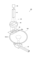
図3に示すように、検査ユニットU3は、筐体30と、保持部31と、リニア駆動部32と、撮像部33と、投光・反射部34と、分光測定部40と、を含む。保持部31は、ウェハWを水平に保持する。リニア駆動部32は、例えば電動モータなどを動力源とし、水平な直線状の経路に沿って保持部31を移動させる。撮像部33は、例えばCCDカメラ等のカメラ35を有する。カメラ35は、保持部31の移動方向において検査ユニットU3内の一端側に設けられており、当該移動方向の他端側に向けられている。投光・反射部34は、撮像範囲に投光し、当該撮像範囲からの反射光をカメラ35側に導く。例えば投光・反射部34は、ハーフミラー36及び光源37を有する。ハーフミラー36は、保持部31よりも高い位置において、リニア駆動部32の移動範囲の中間部に設けられており、下方からの光をカメラ35側に反射する。光源37は、ハーフミラー36の上に設けられており、ハーフミラー36を通して下方に照明光を照射する。
As shown in FIG. 3, the inspection unit U3 includes a
分光測定部40は、ウェハWからの光を入射して分光し、分光スペクトルを取得する機能を有する。分光測定部40は、ウェハWからの光を入射する入射部41と、入射部41に入射した光を導波する導波部42と、導波部42により導波された光を分光して分光スペクトルを取得する分光器43と、光源44と、を有する。入射部41は、保持部31に保持されたウェハWがリニア駆動部32による駆動に伴って移動する際に、ウェハWの中央部からの光を入射可能な構成とされる。すなわち、リニア駆動部32の駆動によって移動する保持部31の中心の移動経路に対応する位置に設けられる。そして、保持部31の移動によってウェハWが移動した際に、ウェハWの径方向に沿ってウェハWの表面に対して入射部41が相対的に移動するように、入射部41が取り付けられる。これにより、分光測定部40は、ウェハWの中心部を含むウェハWの径方向に沿った各位置での分光スペクトルを取得することができる。導波部42は、例えば光ファイバ等によって構成される。分光器43は、入射した光を分光して各波長に対応する強度情報を含む分光スペクトル取得する。光源44は、下方に照明光を照射する。これにより、ウェハWでの反射光が入射部41、導波部42を経て分光器43に入射する。
The
なお、分光器43で取得する分光スペクトルの波長範囲としては、例えば、可視光(380nm~780nm)の波長範囲とすることができる。したがって、可視光を出射する光源を光源44として用いて、光源44からの光に対するウェハW表面での反射光を分光器43で分光することで、可視光の波長範囲の分光スペクトルデータ(分光データ)を得ることができる。なお、分光器43で取得する分光スペクトルの波長範囲は、可視光の範囲に限定されず、例えば、赤外線や紫外線を含む波長範囲としてもよい。取得する分光スペクトルデータの波長範囲に応じて、分光器43及び光源44として適切なものを選択することができる。
The wavelength range of the spectral spectrum obtained by the
検査ユニットU3は、次のように動作してウェハWの表面の画像データを取得する。まず、リニア駆動部32が保持部31を移動させる。これにより、ウェハWがハーフミラー36の下を通過する。この通過過程において、ウェハW表面の各部からの反射光がカメラ35に順次送られる。カメラ35は、ウェハW表面の各部からの反射光を結像させ、ウェハW表面の画像データを取得する。ウェハW表面に形成される膜の膜厚が変化すると、例えば、膜厚に応じて色がウェハW表面の色が変化する等、カメラ35で撮像されるウェハW表面の画像データが変化する。すなわち、ウェハW表面の画像データを取得することは、ウェハWの表面に形成された膜の膜厚に係る情報を取得することに相当する。この点については後述する。
The inspection unit U3 acquires image data of the surface of the wafer W by operating as follows. First, the
カメラ35で取得された画像データは、制御装置100に対して送られる。制御装置100において、画像データに基づいてウェハW表面の膜の膜厚を推定することができ、推定結果が制御装置100において検査結果として保持されることになる。
Image data acquired by the
また、検査ユニットU3による画像データの取得と同時に、分光測定部40においてウェハWの表面からの光を入射して分光測定が行われる。リニア駆動部32が保持部31を移動させる際に、ウェハWは入射部41の下を通過する。この通過過程において、ウェハW表面の各部からの反射光が入射部41に入射し、導波部42を経て分光器43に入射する。分光器43において入射した光を分光し、分光スペクトルデータを取得する。ウェハW表面に形成される膜の膜厚が変化すると、例えば、膜厚に応じて分光スペクトルが変化する。すなわち、ウェハW表面の分光スペクトルデータを取得することは、ウェハWの表面に形成された膜の膜厚に係る情報を取得することに相当する。この点については後述する。検査ユニットU3では、画像データの取得と分光測定とを並行して実施することができる。そのため、これらを個別に行う場合と比較して短時間での計測を行うことができる。
At the same time when the inspection unit U3 acquires the image data, the
分光器43で取得された分光スペクトルデータは、制御装置100に対して送られる。制御装置100において、分光スペクトルデータに基づいてウェハW表面の膜の膜厚を推定することができ、推定結果が制御装置100において検査結果として保持されることになる。
Spectroscopic data acquired by the
[制御装置]
制御装置100の一例について詳細に説明する。制御装置100は、塗布・現像装置2に含まれる各要素を制御する。制御装置100は、ウェハWの表面に上述の各膜を形成させること、及び、現像処理を行うことを含むプロセス処理を実行するように構成されている。また、制御装置100は、プロセス処理におった結果に基づいて、プロセス処理に係るパラメータの補正等も実行するように構成されている。これらのプロセス処理等の詳細については後述する。[Control device]
An example of the
図4に示されるように、制御装置100は、機能上の構成として、検査実施部101、画像情報保持部102、分光測定結果保持部103、膜厚算出部104、及び、判定部105を有する。さらに制御装置100は、詳細検査実施部106、モデル作成部107、モデル保持部108、及び、分光情報保持部109を有する。
As shown in FIG. 4, the
検査実施部101は、検査ユニットU3でのウェハWの検査に係る動作を制御する機能を有する。検査ユニットU3での検査の結果、画像データ及び分光スペクトルデータが取得される。
The
画像情報保持部102は、検査ユニットU3の撮像部33からウェハWの表面を撮像した画像データを取得し、保持する機能を有する。画像情報保持部102において保持される画像データは、ウェハWに形成された膜の膜厚の推定に利用される。なお、ウェハWに形成された膜の膜厚によっては、画像データは膜の膜厚の評価ではなく成膜状態の評価に用いられる場合がある。この点についても後述する。
The image
分光測定結果保持部103は、検査ユニットU3の分光器43からウェハWの表面に係る分光スペクトルデータを取得し、保持する機能を有する。分光測定結果保持部103において保持される分光スペクトルデータは、ウェハWに形成された膜の膜厚の推定に利用される。
The spectroscopic measurement
膜厚算出部104は、画像情報保持部102において保持される画像データ、及び、分光測定結果保持部103において保持される分光スペクトルデータに基づいて、ウェハWに形成された膜の膜厚を算出する機能を有する。膜厚の算出に係る手順の詳細は後述する。
The film
判定部105は、膜厚算出部104で算出された膜厚が適切であるかを判定する機能を有する。膜の形成は、検査ユニットU3の前段の塗布ユニットU1及び熱処理ユニットU2で行われるので、この判定は、塗布ユニットU1及び熱処理ユニットU2が適切に動作しているかどうかの判定に対応する。
The
詳細検査実施部106は、判定部105による判定の結果、膜厚に問題があると判定された場合、塗布ユニットU1及び熱処理ユニットU2の動作を確認するための詳細検査を実施する機能を有する。詳細検査については後述するが、パターンが形成されていないベアウェハを検査用のウェハとして準備し、当該ウェハに対して膜の形成を行いその膜厚を評価する。
The detailed
モデル作成部107及びモデル保持部108は、画像データから膜厚を算出する際に使用するモデルを作成し、保持する機能を有する。検査ユニットU3で撮像される画像データからはウェハWの表面の色情報を取得することができる。そこで、モデル作成部107においてウェハW表面の色情報に基づいて膜厚を推定することが可能なモデルを作成し、モデル保持部108において作成したモデルを保持する。膜厚算出部104では、当該モデルを利用して検査対象のウェハWについて膜厚を推定する。
The
分光情報保持部109は、分光スペクトルデータから膜厚を算出する際に使用する分光情報を保持する機能を有する。検査ユニットU3で取得される分光スペクトルデータは、ウェハW表面に形成される膜の種類及び膜厚によって変化する。そこで、分光情報保持部109において膜厚と分光スペクトルとの対応関係に係る情報を保持する。膜厚算出部104では、分光情報保持部109において保持される情報に基づいて検査対象のウェハW(対象基板)について膜厚を推定する。
The spectral
制御装置100は、一つ又は複数の制御用コンピュータにより構成される。例えば制御装置100は、図5に示される回路120を有する。回路120は、一つ又は複数のプロセッサ121と、メモリ122と、ストレージ123と、入出力ポート124とを有する。ストレージ123は、例えばハードディスク等、コンピュータによって読み取り可能な記憶媒体を有する。記憶媒体は、後述のプロセス処理手順を制御装置100に実行させるためのプログラムを記憶している。記憶媒体は、不揮発性の半導体メモリ、磁気ディスク及び光ディスク等の取り出し可能な媒体であってもよい。メモリ122は、ストレージ123の記憶媒体からロードしたプログラム及びプロセッサ121による演算結果を一時的に記憶する。プロセッサ121は、メモリ122と協働して上記プログラムを実行することで、上述した各機能モジュールを構成する。入出力ポート124は、プロセッサ121からの指令に従って、制御対象の部材との間で電気信号の入出力を行う。
The
なお、制御装置100のハードウェア構成は、必ずしもプログラムにより各機能モジュールを構成するものに限られない。例えば制御装置100の各機能モジュールは、専用の論理回路又はこれを集積したASIC(Application Specific Integrated Circuit)により構成されていてもよい。
Note that the hardware configuration of the
なお、図4及び以下の実施形態では、制御装置100内に上記構成が含まれている場合について説明するが、制御装置100に上記の全機能が含まれていなくてもよい。例えば、モデル作成部107及びモデル保持部108を含むモデル管理部110、または、モデル作成部107のみが、外部装置に設けられる構成であってもよい。換言すると、これらの機能は例えば、塗布・現像装置2を制御する制御装置100とは異なる装置に設けられていてもよい。このように、モデルの作成に係る機能が制御装置100とは外部装置に設けられている場合、外部装置と制御装置100とが連携して以下の実施形態で説明する機能を発揮する。また、このような場合、本実施形態で説明する制御装置100に対応する機能が搭載された外部装置と、本実施形態で説明する基板処理装置と、が一体的に基板検査システムとして機能し得る。
In addition, although FIG. 4 and the following embodiments describe the case where the above configuration is included in the
[プロセス処理手順]
続いて、塗布・現像処理の一例として塗布・現像装置2において実行されるプロセス処理手順について説明する。[Process procedure]
Next, as an example of the coating/developing process, a process procedure performed in the coating/developing
プロセス処理手順において、まず制御装置100は、キャリアC内のプロセス処理対象のウェハWを棚ユニットU10に搬送するように搬送装置A1を制御し、このウェハWを処理モジュール11用のセルに配置するように搬送装置A7を制御する。
In the process procedure, the
次に制御装置100は、棚ユニットU10のウェハWを処理モジュール11内の塗布ユニットU1及び熱処理ユニットU2に搬送するように搬送装置A3を制御する。また、制御装置100は、このウェハWの表面上に下層膜を形成するように塗布ユニットU1及び熱処理ユニットU2を制御する。なお、下層膜の形成後、制御装置100は、ウェハWを検査ユニットU3に搬送するように搬送装置A3を制御し、検査ユニットU3を用いて当該ウェハWの表面の状態を検査してもよい。その後制御装置100は、下層膜が形成されたウェハWを棚ユニットU10に戻すように搬送装置A3を制御し、このウェハWを処理モジュール12用のセルに配置するように搬送装置A7を制御する。
Next, the
次に制御装置100は、棚ユニットU10のウェハWを処理モジュール12内の塗布ユニットU1及び熱処理ユニットU2に搬送するように搬送装置A3を制御する。また、制御装置100は、このウェハWの下層膜上に中間膜を形成するように塗布ユニットU1及び熱処理ユニットU2を制御する。例えば、制御装置100は、ウェハWの下層膜上に中間膜形成用の処理液を塗布することによって中間膜を形成するように塗布ユニットU1を制御する。次に、制御装置100は、中間膜に熱処理を施すように熱処理ユニットU2を制御する。中間膜の形成後、制御装置100は、ウェハWを検査ユニットU3に搬送するように搬送装置A3を制御し、検査ユニットU3を用いて当該ウェハWの表面の状態を検査するように制御する。その後制御装置100は、ウェハWを棚ユニットU10に戻すように搬送装置A3を制御し、このウェハWを処理モジュール13用のセルに配置するように搬送装置A7を制御する。
Next, the
次に制御装置100は、棚ユニットU10のウェハWを処理モジュール13内の各ユニットに搬送するように搬送装置A3を制御し、このウェハWの中間膜上にレジスト膜を形成するように塗布ユニットU1及び熱処理ユニットU2を制御する。例えば、制御装置100は、ウェハWの中間膜上にレジスト膜形成用の処理液を塗布することによってレジスト膜を形成するように塗布ユニットU1を制御する。次に、制御装置100は、レジスト膜に熱処理を施すように熱処理ユニットU2を制御する。なお、レジスト膜の形成後、制御装置100は、ウェハWを検査ユニットU3に搬送するように搬送装置A3を制御し、検査ユニットU3を用いて当該ウェハWの表面の状態(例えば、上層膜の膜厚)を検査してもよい。その後制御装置100は、ウェハWを棚ユニットU11に搬送するように搬送装置A3を制御する。
Next, the
次に制御装置100は、棚ユニットU11のウェハWを露光装置3に送り出すように搬送装置A8を制御する。その後制御装置100は、露光処理が施されたウェハWを露光装置3から受け入れて、棚ユニットU11における処理モジュール14用のセルに配置するように搬送装置A8を制御する。
Next, the
次に制御装置100は、棚ユニットU11のウェハWを処理モジュール14内の各ユニットに搬送するように搬送装置A3を制御し、このウェハWのレジスト膜に現像処理を施すように塗布ユニットU1及び熱処理ユニットU2を制御する。その後制御装置100は、ウェハWを棚ユニットU10に戻すように搬送装置A3を制御し、このウェハWをキャリアC内に戻すように搬送装置A7及び搬送装置A1を制御する。以上でプロセス処理が完了する。
Next, the
[基板検査方法]
次に、図6~図11を参照しながら、制御装置100による処理モジュール11~13における基板検査方法について説明する。基板検査方法は、処理モジュール11~13に設けられた検査ユニットU3において行われる成膜後のウェハWの検査に係る方法である。検査ユニットU3では、成膜後のウェハWにおいて所望の成膜が実施されたかを検査する。具体的には、ウェハW上に形成された膜の表面の状態及び膜厚の評価を行う。検査ユニットU3は、上述の通り例えば撮像部33及び分光測定部40を有しているので、撮像部33によりウェハWの表面を撮像した画像データと、分光測定部40によりウェハWの表面の分光スペクトルデータとを取得することができる。制御装置100では、これらのデータに基づいて成膜状況を評価する。なお、ウェハWの成膜状況を評価する目的から、処理モジュール11~13における下層膜、中間膜、レジスト膜のそれぞれを成膜した後に、検査ユニットU3による検査を行うことができる。[Board inspection method]
Next, a substrate inspection method in the
図6は、検査ユニットU3における基板検査方法の一連の流れを説明するフロー図である。まず、制御装置100は、ステップS01を実行する。ステップS01では、塗布ユニットU1及び熱処理ユニットU2において成膜が行われたウェハWを検査ユニットU3に搬入する。ウェハWは保持部31において保持される。
FIG. 6 is a flow diagram for explaining a series of flows of the board inspection method in the inspection unit U3. First, the
次に、制御装置100の検査実施部101は、ステップS02(画像取得ステップ)を実行する。ステップS02では、撮像部33によりウェハWの表面を撮像する。具体的には、リニア駆動部32の駆動により保持部31を所定の方向に移動させながら撮像部33によりウェハW表面の撮像を行う。これにより、撮像部33においてウェハWの表面に係る画像データが取得される。画像データは、制御装置100の画像情報保持部102において保持される。
Next, the
なお、ステップS02の実施と同時に、制御装置100の検査実施部101は、ステップS03(分光測定ステップ)を実行する。ステップS03では、分光測定部40によりウェハWの表面の1ラインの分光測定を行う。上述のように、分光測定部40の入射部41は、保持部31が移動する際に保持部31に保持されたウェハWの中心が通過する経路上に設けられるので、ウェハWの中心部を含むウェハWの径方向に沿った各位置での分光スペクトルを取得することができる。したがって、図7に示すように、入射部41には、ウェハWの中心を通る中心線Lに沿った表面での反射光が入射する。分光器43では、所定の間隔で入射した光の分光スペクトルに係る測定を行う。その結果、分光器43では、中心線Lに沿った複数箇所として、例えば、図7に示すP1~Pnのn個の位置に対応した分光スペクトルデータを取得する。このように、分光器43を用いることでウェハWの中心線Lに沿った複数箇所でのウェハW表面に係る分光スペクトルデータが取得される。なお、nは分光器43による分光測定の間隔と、保持部31によるウェハWの移動速度とによって適宜変更することができる。分光器43で取得された分光スペクトルデータは、制御装置100の分光測定結果保持部103において保持される。Simultaneously with execution of step S02,
制御装置100の膜厚算出部104は、ステップS04を実行する。ステップS04では、ウェハW表面に係る画像データまたは分光測定による分光スペクトルデータに基づいて、ウェハW表面の膜の膜厚を算出する。
The
画像データを用いて膜厚を算出する場合の手順について、図8を参照しながら説明する。画像データを用いた膜厚の算出では、モデル作成部107によって作成されてモデル保持部108において保持される膜厚モデルが使用される。膜厚モデルとは、所定の膜を形成した際のウェハW表面を撮像した画像データにおける各画素の色の変化に係る情報(所定の膜を形成する前と後の色の変化)から膜厚を算出するためのモデルであり、色の変化に係る情報と膜厚との対応関係を示したモデルである。このようなモデルを予め制御装置100のモデル作成部107で作成し、モデル保持部108で保持することにより、画像データの各位置における色の変化に係る情報を取得することで、当該色の変化から膜厚を推定することができる。膜厚モデルの作成方法については後述するが、前段までの各処理を行ったウェハWと、その後の所定の膜を形成したウェハWと、の両方について、その表面の撮像を行って画像データを取得し、色がどのように変化したかを特定する。また、同一条件で成膜したウェハにおける膜厚の計測を行う。これにより膜厚と色の変化との対応関係を特定することができる。膜厚を変更しながらこの計測を繰り返すことで、色の変化に係る情報と膜厚との対応関係を得ることができる。
A procedure for calculating the film thickness using image data will be described with reference to FIG. In the film thickness calculation using image data, a film thickness model created by the
画像データからの膜厚の算出方法は、具体的には、図8に示す通りである。まず、撮像した画像データを取得(ステップS11)した後、当該画像データから画素毎の色の変化に係る情報を取得する(ステップS12)。色の変化に係る情報を取得するためには、成膜前の画像データとの差分を算出する処理を行うことができる。その後、モデル保持部108で保持される膜厚モデルとの比較を行う(ステップS13)。これにより、画素毎に当該画素が撮像した領域の膜厚を推定することができる(ステップS14)。これにより、画素毎、すなわち、ウェハW表面の各位置での膜厚を推定することが可能となる。
Specifically, the method for calculating the film thickness from the image data is as shown in FIG. First, after acquiring captured image data (step S11), information relating to color change for each pixel is acquired from the image data (step S12). In order to obtain information related to color change, a process of calculating a difference from image data before film formation can be performed. After that, comparison with the film thickness model held in the
なお、上記の画像データに基づく膜厚の算出(推定)は、ウェハW上に形成する膜が比較的薄い場合(例えば、500nm以下程度)は可能であるが、膜厚が大きくなると難しい。これは、膜厚が大きくなると、膜厚の変化に対する色の変化が少なくなるため、色の変化に係る情報から膜厚を精度よく推定することが困難となるためである。したがって、膜厚が大きな膜を形成した場合には、膜厚の推定は分光スペクトルデータに基づいて行われる。 The calculation (estimation) of the film thickness based on the above image data is possible when the film formed on the wafer W is relatively thin (for example, about 500 nm or less), but is difficult when the film thickness is large. This is because as the film thickness increases, the change in color with respect to the change in film thickness decreases, making it difficult to accurately estimate the film thickness from the information relating to the change in color. Therefore, when a film having a large film thickness is formed, the film thickness is estimated based on spectral data.
分光スペクトルデータを用いて膜厚を算出する場合の手順について、図9を参照しながら説明する。分光スペクトルデータを用いた膜厚の算出とは、表面の膜の膜厚に応じた反射率の変化を利用するものである。表面に膜が形成されたウェハに対して光を照射すると、光が最上位の膜の表面で反射するか、または最上位の膜とその下層(の膜またはウェハ)との界面で反射する。そして、これらの光が反射光として出射される。すなわち、反射光には、位相が異なる2つの成分の光が含まれる。また、表面の膜厚が大きくなると、その位相差が大きくなる。したがって、膜厚が変化すると、上記の膜表面で反射された光と、下層との界面で反射された光との干渉の度合いが変化する。すなわち、反射光の分光スペクトルの形状に変化が生じる。膜厚に応じての分光スペクトルの変化は、理論上算出することができる。したがって制御装置100では、表面に形成される膜の膜厚に応じた分光スペクトルの形状に係る情報を予め保持しておく。そして、実際のウェハWに対して光を照射して得られる反射光の分光スペクトルと、予め保持している情報とを比較する。これにより、ウェハWの表面の膜の膜厚を推定することが可能となる。膜厚の推定に用いられる膜厚と分光スペクトルの形状との関係に係る情報は、制御装置100の分光情報保持部109に保持される。
A procedure for calculating the film thickness using spectral data will be described with reference to FIG. Calculation of the film thickness using spectroscopic data utilizes changes in reflectance according to the film thickness of the film on the surface. When a wafer having a film formed on its surface is irradiated with light, the light is reflected on the surface of the uppermost film or reflected at the interface between the uppermost film and its lower layer (film or wafer). These lights are emitted as reflected lights. That is, the reflected light contains two light components with different phases. Further, as the film thickness on the surface increases, the phase difference increases. Therefore, when the film thickness changes, the degree of interference between the light reflected on the film surface and the light reflected on the interface with the lower layer changes. That is, a change occurs in the shape of the spectrum of the reflected light. The change in the spectral spectrum depending on the film thickness can be theoretically calculated. Therefore, the
分光スペクトルデータからの膜厚の算出方法は、具体的には、図9に示す通りである。まず、分光測定の結果、すなわち、分光スペクトルデータを取得(ステップS21)した後、当該分光スペクトルデータを、分光情報保持部109で保持する情報、すなわち、理論上の膜厚に対応する分光スペクトルの形状に係る情報と比較する(ステップS22)。これにより、分光スペクトルデータ毎に当該分光スペクトルデータが得られた領域の膜厚を推定することができる(ステップS23)。これにより、分光スペクトルデータ毎、すなわち、ウェハW表面の各位置での膜厚を推定することが可能となる。上述のように、1枚のウェハWにおいて、中心線Lに沿った複数箇所において分光スペクトルデータが得られるため、各分光スペクトルデータに基づいて膜厚を算出することで、ウェハW表面での膜厚の分布に係る情報を得ることができる。
Specifically, the method for calculating the film thickness from the spectroscopic data is as shown in FIG. First, after acquiring the result of spectroscopic measurement, that is, spectroscopic data (step S21), the spectroscopic data is stored in the spectroscopic
撮像部33で撮像されるウェハWの画像データは、ウェハW表面の全体を撮像したものになるので、ウェハW表面全体の膜厚を画像データから推定することが可能である。一方、分光測定部40により取得する分光スペクトルデータに基づく膜厚の推定では、分光スペクトルデータを取得する箇所がウェハWの中心線L上に限定される。したがって、分光スペクトルデータに基づくウェハW表面の膜の膜厚の推定では、画像データに基づく膜厚の推定と比較して、全体的な膜厚の分布を評価することは難しい。ただし、上記の1ラインでの分光測定によっても中心線Lに沿って複数箇所の膜厚を推定することは可能である。したがって、ウェハW表面に形成される膜の膜厚の面内分布に異常がある場合には、複数の分光スペクトルデータから推定される膜厚にばらつきが生じる等何らかの変化を検出することが可能であると考えられる。
Since the image data of the wafer W imaged by the
上記のように、画像データに基づく膜厚の推定は、ウェハWに形成する膜がある程度薄い場合に限定される。一方、分光スペクトルデータに基づく膜厚の推定は、ウェハWに形成する膜がある程度厚くても可能であるだけでなく、膜厚が小さい(例えば、数十nm等)場合であっても可能である。このように、分光スペクトルデータに基づく膜厚の推定はウェハWの厚さに限定されにくいため汎用性が高いと考えられる。ただし、ウェハWには所定のパターンが形成されている。そのため、パターンの凹凸の影響を受けた分光スペクトルデータが得られる可能性もある。そのため、ウェハWから取得された分光スペクトルデータは、ウェハWに形成された膜の膜厚が正確に反映したものとは限らない可能性がある。その点を考慮して分光スペクトルデータを取り扱う必要がある。また、分光スペクトルデータから推定される膜厚についても正確ではない可能性があることを考慮することが求められる。ただし、この問題は、分光スペクトルデータを取得する位置をより精度良く特定できると解決し得る。すなわち、パターニングされているウェハWの表面に係る分光スペクトルを取得する際に、段差が形成される位置とは異なる位置において分光スペクトルデータを取得できるように制御可能であると、パターンに由来する精度の低下を避けることができる。 As described above, the film thickness estimation based on the image data is limited to the case where the film formed on the wafer W is thin to some extent. On the other hand, the estimation of the film thickness based on the spectroscopic data is possible not only when the film formed on the wafer W is thick to some extent, but also when the film thickness is small (for example, several tens of nanometers). be. In this way, the estimation of the film thickness based on the spectroscopic data is less likely to be limited to the thickness of the wafer W, so it is considered to have high versatility. However, the wafer W has a predetermined pattern formed thereon. Therefore, there is a possibility that spectroscopic data affected by the unevenness of the pattern can be obtained. Therefore, the spectral data acquired from the wafer W may not necessarily reflect the film thickness of the film formed on the wafer W accurately. Spectroscopic data must be handled with this point in mind. In addition, it is required to take into account the possibility that the film thickness estimated from spectroscopic data may not be accurate. However, this problem can be solved if the position from which spectroscopic data is acquired can be specified with higher accuracy. That is, when acquiring the spectral spectrum of the patterned surface of the wafer W, it is possible to obtain the spectral data at a position different from the position where the step is formed. can be avoided.
膜厚の推定を分光スペクトルデータに基づいて行う場合、画像データは、例えば、成膜状況の評価に用いることができる。成膜状況の評価とは、膜表面にスポットなどの欠損がないか等の画像データから検出できる異常がないかというものである。そのため、画像データと分光スペクトルデータの両方を取得することで、成膜状況をより詳細に評価することができる。例えば、分光スペクトルデータを取得する対象となるウェハWの中心線L上の一部の領域に欠損があることが画像データから検出できたとする。この場合、その領域に重複又は隣接する箇所の分光スペクトルデータを特定して当該分光スペクトルデータを膜厚推定の平均値の算出には利用しないことで、推定値の精度を上げることができる。また、欠損領域に対応する画像とその箇所の分光スペクトルデータに基づく膜厚推定値とを自動的に関連づけて記憶しておくこともできる。これにより、欠損が生じた平面領域における深さ方向の情報を簡単かつ確実に取り出せるので、例えば、事後的に欠損の状態や生じた理由等を解析する作業の効率化や高精度化が図れる。このように、画像データに基づいて基板の表面における成膜状況の評価を行う構成とすることで、画像データから得られる成膜状況に応じて分光スペクトルデータを広く活用することができる。 When the film thickness is estimated based on spectral data, the image data can be used, for example, to evaluate the film formation status. Evaluation of the film formation state means whether or not there is an abnormality that can be detected from the image data, such as whether or not there is a defect such as a spot on the film surface. Therefore, by obtaining both the image data and the spectrum data, the film formation state can be evaluated in more detail. For example, it is assumed that it is possible to detect from the image data that there is a defect in a part of the area on the center line L of the wafer W for which spectral data is to be acquired. In this case, the accuracy of the estimated value can be improved by specifying the spectroscopic data of a portion overlapping or adjacent to the region and not using the spectroscopic data for calculating the average value of the film thickness estimation. It is also possible to automatically associate and store an image corresponding to the missing region and the estimated film thickness value based on the spectroscopic data of that location. As a result, information in the depth direction in a plane region where a defect has occurred can be obtained easily and reliably, so that, for example, it is possible to improve the efficiency and accuracy of post-analysis of the state of the defect and the reason for the occurrence of the defect. In this way, by adopting a configuration in which the film formation state on the surface of the substrate is evaluated based on the image data, it is possible to widely utilize the spectral data according to the film formation state obtained from the image data.
なお、膜厚の推定を画像データに基づいて行う場合には、分光スペクトルデータの取得(ステップS03)を省略してもよい。この場合、分光測定部40による分光スペクトルデータ自体を行わず、画像データのみに基づいて、膜厚の推定及び成膜状況の評価を行う構成としてもよい。
Note that when the film thickness is estimated based on the image data, the acquisition of spectral data (step S03) may be omitted. In this case, a configuration may be adopted in which the estimation of the film thickness and the evaluation of the film formation state are performed based only on the image data without performing the spectroscopic data itself by the
図6に戻り、膜厚の算出(ステップS04)の後、制御装置100の検査実施部101は、ステップS05を実行する。ステップS05では、ウェハWを検査ユニットU3から搬出する。搬出されたウェハWは、例えば、後段の処理モジュールに送られる。
Returning to FIG. 6, after calculating the film thickness (step S04), the
次に、制御装置100の判定部105は、ステップS06(判定ステップ)を実行する。ステップS06では、ウェハWの膜厚が合格基準に達しているかを確認する。合格基準とは、ウェハW全体の膜厚が所定の膜厚の設定範囲に含まれているか否かに基づくものである。すなわち、ステップS06は、前段の塗布ユニットU1及び熱処理ユニットU2において、適切に成膜が行われたかの評価を行うものである。
Next, the
ステップS06での膜厚の合否判定に係る基準について、図10を参照しながら説明する。ウェハWに形成される膜には、それぞれ膜厚の設定値(設定範囲)が定められている。図10では、膜厚の設定範囲Dを示すと共に、複数のウェハWの膜厚の推定結果を時系列にそれぞれドットとして示している。上述のように、画像データ及び分光スペクトルデータの何れに基づいても1枚のウェハWの表面の複数箇所の膜厚が推定される。図10では、1枚のウェハWにおける複数箇所での膜厚の平均値の推定結果を示しているとする。ここでは、同一の基板処理を行うウェハWに対して、1ロット(25枚)毎に1枚を推定用にサンプリングした例を示しているが、これに限らず、例えば、10枚を処理するごとに1枚、1時間経過するごとに1枚といった単位でも良い。 The criteria related to the pass/fail determination of the film thickness in step S06 will be described with reference to FIG. Each film formed on the wafer W has a set value (set range) of film thickness. In FIG. 10, the set range D of the film thickness is shown, and the estimation results of the film thicknesses of the plurality of wafers W are shown as dots in chronological order. As described above, the film thickness at a plurality of locations on the surface of one wafer W is estimated based on both the image data and the spectrum data. In FIG. 10, it is assumed that estimation results of the average value of the film thickness at a plurality of locations on one wafer W are shown. Here, an example is shown in which one sample is sampled for estimation from each lot (25 wafers) of the wafers W subjected to the same substrate processing. The unit may be one sheet every time, or one sheet every time one hour elapses.
ここで、時系列に沿って処理された複数枚のウェハWに係る全ての箇所での膜厚の推定結果が設定範囲Dに含まれている場合には、ウェハWは合格であると判定することができる。一方、図10においてX1として示すように、設定範囲Dから外れている膜厚の推定結果が現れた場合には、合格基準に達して以内と判定することができる。また、合格基準として膜厚の偏りを考慮する構成としてもよい。例えば、分光スペクトルデータからの膜厚の推定の場合、図10の実線X2または実線X3で示すように、時系列に沿って処理された複数の膜厚の推定結果が設定範囲Dから徐々に外れるように推移している結果が得られる場合がある。この場合、現段階では当該ウェハWの膜厚の推定結果は設定範囲Dに含まれているとしても、将来的には膜厚が設定範囲Dから外れていく可能性も考えられる。そのため、当該ウェハWについて不合格と判定した上で、装置に係る詳細な検査(後述のQC検査)を行うように構成してもよい。このように、ステップS06での膜厚の合否判定を行う際の基準(合格基準)は、時系列の変化状況に応じて適宜変更してもよい。 Here, when the estimation results of the film thickness at all locations of a plurality of wafers W processed in chronological order are included in the set range D, the wafer W is determined to be acceptable. be able to. On the other hand, as indicated by X1 in FIG. 10, when the estimation result of the film thickness outside the set range D appears, it can be determined that the acceptance criteria are met. Moreover, it is good also as a structure which considers the bias|inclination of a film thickness as acceptance criteria. For example, in the case of estimating the film thickness from spectroscopic data, as indicated by the solid line X2 or the solid line X3 in FIG. You may get results that are trending like this. In this case, even if the estimated film thickness of the wafer W is within the set range D at the present stage, the film thickness may deviate from the set range D in the future. Therefore, after determining that the wafer W is rejected, a detailed inspection (QC inspection to be described later) of the apparatus may be performed. In this manner, the criteria (acceptance criteria) for judging whether or not the film thickness is acceptable in step S06 may be appropriately changed in accordance with the chronological changes.
膜厚に係る合否判定が合格である場合(S06-YES)、制御装置100の検査実施部101は、ステップS07を実行する。ステップS07では、次のウェハWに係る検査を行うか判定し、検査を終了するか(S07-YES)、次のウェハWに係る検査を開始する(S07-NO)。
If the pass/fail determination regarding the film thickness is pass (S06-YES), the
一方、膜厚に係る合否判定が不合格である場合(S06-NO)、制御装置100は詳細検査を行うと判断し、詳細検査実施部106により、ステップS08を実行する。ステップS08とは、膜厚に係る詳細検査(QC検査)である。
On the other hand, if the pass/fail determination regarding the film thickness is rejected (S06-NO), the
詳細検査とは、QCウェハ(検査用基板)と呼ばれるベアウェハ(表面にパターニング等が行われていないウェハ)を用いた検査である。QCウェハを塗布ユニットU1及び熱処理ユニットU2に搬入し、通常のウェハと同じ条件で成膜を行った後に、検査ユニットU3において通常のウェハよりもより詳細に膜厚の評価を行うことを詳細検査という。この詳細検査は、特に、通常のウェハWでは分光スペクトルデータを用いた膜厚の推定を行っている場合に有用である。通常のウェハWに係る検査で分光スペクトルデータを用いて膜厚を評価している場合、通常のウェハWについてはウェハWの表面全体の膜厚分布を評価しているわけではない。したがって、合否判定(ステップS06)でウェハWが不合格であると判定された場合、膜厚の推定を行っていない領域についてどのような膜厚となっているかを把握することが必要となる。詳細検査とは、この検査に対応するものである。 A detailed inspection is an inspection using a bare wafer (a wafer whose surface is not subjected to patterning or the like) called a QC wafer (substrate for inspection). After carrying the QC wafer into the coating unit U1 and the heat treatment unit U2 and performing film formation under the same conditions as for a normal wafer, the detailed inspection is to evaluate the film thickness in more detail than the normal wafer in the inspection unit U3. It says. This detailed inspection is particularly useful when estimating the film thickness of a normal wafer W using spectral data. When the film thickness is evaluated using spectroscopic data in the normal inspection of the wafer W, the film thickness distribution over the entire surface of the normal wafer W is not evaluated. Therefore, when the wafer W is determined to be unacceptable in the pass/fail determination (step S06), it is necessary to grasp what kind of film thickness is in the region where the film thickness is not estimated. A detailed inspection corresponds to this inspection.
詳細検査の手順について図11を参照しながら説明する。まず、制御装置100の詳細検査実施部106は、ステップS31を実行する。ステップS31では、塗布ユニットU1及び熱処理ユニットU2での成膜処理が終わったQCウェハを検査ユニットU3に搬入する。すなわち、QCウェハは、対象基板であるウェハWと同じ条件での成膜処理を行った(成膜ステップ)後に、検査ユニットU3に搬入される。搬入されたQCウェハは保持部31において保持される。
A detailed inspection procedure will be described with reference to FIG. First, the detailed
次に、制御装置100の詳細検査実施部106は、ステップS32(詳細測定ステップ)を実行する。ステップS32では、面内の色々な場所で膜厚を測定する。膜厚の測定の際には、分光スペクトルデータを多点で取得する。膜厚の測定を行う点は、QCウェハの表面全体に分散させる。通常のウェハWの場合には、画像データの取得と同時に分光スペクトルデータの取得が行われるため、保持部31の一方向への移動にあわせて、ウェハWの中心線Lに沿って複数の分光スペクトルデータを取得している。これに対して、面内多点での膜厚測定では、保持部31において保持するQCウェハの向きを変更させながら、保持部31を移動させる。これにより、検査ユニットU3を利用してウェハ表面において2次元状に分散配置された種々の測定位置での分光スペクトルデータを取得することができる。
Next, the detailed
分光スペクトルデータが取得されると、制御装置100の膜厚算出部104は、ステップS33(詳細測定ステップ)を実行する。ステップS33では、ウェハW表面に係る複数の分光スペクトルデータのそれぞれに基づいて、ウェハW表面の膜の膜厚を算出し、面内の膜厚分布の算出を行う。なお、分光スペクトルデータを用いて膜厚を算出する場合の手順は、通常のウェハWに係る膜厚の算出と同じ方法を用いることができ、具体的には、図9に示す通りである。
When the spectral data is acquired, the
膜厚分布の算出(ステップS33)の後、制御装置100の詳細検査実施部106は、ステップS34を実行する。ステップS34では、QCウェハを検査ユニットU3から搬出する。搬出されたウェハWは、例えば、後段の処理モジュールに送られる。
After calculating the film thickness distribution (step S33), the detailed
次に、制御装置100の判定部105は、ステップS35を実行する。ステップS35では、ウェハWの膜厚が合格基準に達しているかを確認する。ここでの合格基準とは、QCウェハの表面で測定された膜厚分布が所定の膜厚の設定範囲に含まれているか否かに基づくものである。すなわち、ステップS33は、前段の塗布ユニットU1及び熱処理ユニットU2において、ウェハ表面の全体において適切に成膜が行われたかの評価を行うものである。
Next, the
膜厚分布に係る合否判定が合格である場合(S35-YES)、制御装置100の詳細検査実施部106は、一連の処理を終了する。一方、膜厚分布に係る合否判定が不合格である場合(S35-NO)、制御装置100の詳細検査実施部106では、エラーメッセージを発信する等により、成膜が適切に行われていないことをオペレータ等に通知する。そして、膜厚が適切になっていない原因を調査すると共に(ステップS36)、原因に係る部分について調整を行う(ステップS37)。その後、再度QCウェハを導入して(ステップS31)一連の詳細検査を行う。原因の調査(ステップS37)及び調整(ステップS38)は、制御装置100によって主体的に行う構成としてもよい。また、これらのステップは、例えば、制御装置100はエラー通知のみを行う構成として、制御装置100(基板処理システム1)のオペレータ等が制御装置100を操作することによって行われてもよい。
If the pass/fail determination regarding the film thickness distribution is pass (S35-YES), the detailed
詳細検査(QC検査)は、ウェハ表面の膜厚の面内分布に係る合否判定(ステップS35)が合格となるまで繰り返し行われる。換言すると、この合否判定(ステップS35)が合格となると、通常のウェハWに係る成膜を再開することができるともいえる。すなわち、図6に示すように、処理を終了しない場合(S07-NO)には、通常のウェハWを搬入した検査を再開することができる。 The detailed inspection (QC inspection) is repeated until the pass/fail judgment (step S35) regarding the in-plane distribution of the film thickness on the wafer surface is passed. In other words, it can be said that normal film formation on the wafer W can be resumed when the pass/fail determination (step S35) is passed. That is, as shown in FIG. 6, if the process is not finished (S07-NO), the normal inspection with the loaded wafer W can be resumed.
[基板検査方法で使用するモデルの作成方法]
次に、図12,図13を参照しながら、制御装置100による基板検査方法で用いるモデル(膜厚モデル)の作成方法について説明する。上述したように、膜厚モデルは、膜厚と画像データの色情報の対応関係とを対応付けたものである。したがって、膜厚が既知のウェハWについて、そのウェハWを撮像した画像データから色情報を特定することで、膜厚と色情報との対応関係を取得することができる。ウェハに対して成膜を行った場合の膜厚を正確に測定するためには、パターニングが行われていないウェハ(ベアウェハ)に対して成膜を行った場合の膜厚を断面計測等によって測定することが求められる。[How to create a model used in the board inspection method]
Next, referring to FIGS. 12 and 13, a method of creating a model (film thickness model) used in the substrate inspection method by the
そこで、膜厚モデルで使用する膜厚情報及び色情報を取得する。ここでは、色情報の取得するために用いられるパターニングが行われていないベアウェハ(色情報用基板)と、膜厚を測定するために用いられるパターニングが行われていないベアウェハ(膜厚測定用基板)とが用いられる。 Therefore, the film thickness information and color information used in the film thickness model are obtained. Here, a bare wafer without patterning (color information substrate) used for acquiring color information and a bare wafer without patterning (film thickness measurement substrate) used for measuring film thickness are shown. and are used.
図12を参照しながら、制御装置100によるモデル作成のうち、色情報用基板であるベアウェハを用いた色情報の取得方法について説明する。
With reference to FIG. 12, a method of acquiring color information using a bare wafer, which is a substrate for color information, in model creation by the
まず、制御装置100のモデル作成部107は、ステップS41を実行する。ステップS41では、色情報用基板の準備が行われる。色情報用基板として上述のようにベアウェハを準備する。また、この段階で色情報用基板として用いられるベアウェハを検査ユニットU3において撮像することで、成膜前の基板に係る画像データを取得する。このとき得られる画像データは、下層膜を形成した後のウェハの表面の色情報の取得に利用される。
First, the
次に、制御装置100のモデル作成部107は、ステップS42を実行する。ステップS42では、処理モジュール11の各ユニットを制御することで、準備された色情報用基板対して下層膜の形成が行われる。ここでは、予め定められた設定で下層膜の形成を行う。
Next, the
次に、制御装置100のモデル作成部107は、ステップS43を実行する。ステップS43では、処理モジュール11の検査ユニットU3を制御することで、下層膜が形成された色情報用基板の表面に係る画像データを取得する。このとき得られる画像データは、下層膜を形成した後のウェハの表面の色情報の取得に利用される。
Next, the
次に、制御装置100のモデル作成部107は、ステップS44を実行する。ステップS44では、処理モジュール12の各ユニットを制御することで、色情報用基板の下層膜上に中間膜の形成が行われる。ここでは、予め定められた設定で中間膜の形成を行う。
Next, the
次に、制御装置100のモデル作成部107は、ステップS45を実行する。ステップS45では、処理モジュール12の検査ユニットU3を制御することで、中間膜が形成された色情報用基板の表面に係る画像データを取得する。このとき得られる画像データは、中間膜を形成した後のウェハの表面の色情報の取得に利用される。
Next, the
次に、制御装置100のモデル作成部107は、ステップS46を実行する。ステップS46では、処理モジュール13の各ユニットを制御することで、色情報用基板の中間膜上にレジスト膜の形成が行われる。ここでは、予め定められた設定で中間膜の形成を行う。
Next, the
次に、制御装置100のモデル作成部107は、ステップS47を実行する。ステップS47では、処理モジュール13の検査ユニットU3を制御することで、レジスト膜が形成された色情報用基板の表面に係る画像データを取得する。このとき得られる画像データは、レジスト膜を形成した後のウェハの表面の色情報の取得に利用される。
Next, the
このように、色情報用基板については、実際のウェハWに係る基板処理工程と同様に、下層膜、中間膜、レジスト膜の成膜を行うと共に、膜を形成する度に画像データの取得を行う。これにより、ウェハWの成膜時と同様の条件で製造された色情報用基板の表面の画像データを取得することができる。 As described above, for the color information substrate, the lower layer film, the intermediate film, and the resist film are formed in the same manner as in the substrate processing process for the actual wafer W, and image data is acquired each time the film is formed. conduct. As a result, image data of the surface of the color information substrate manufactured under the same conditions as when the film was formed on the wafer W can be acquired.
次に、図13を参照しながら、制御装置100によるモデル作成における手順のうち、膜厚測定用基板を用いた膜厚情報の取得方法について説明する。膜厚測定用基板は、所定の条件で成膜を行った際にウェハ上に形成される膜厚を正確に算出するために用いられる。したがって、下層膜、中間膜、レジスト膜の3種類の膜をウェハ上に形成する場合、各膜の形成の際に、下層に他の膜が形成されていないベアウェハを用いる。これにより、他の膜が下層に設けられることによる膜厚の微妙な変化等の影響を受けることなく正確に膜厚を測定することができる。
Next, a method for obtaining film thickness information using a film thickness measurement substrate, which is part of the procedure for creating a model by the
まず、制御装置100のモデル作成部107は、ステップS51を実行する。ステップS51では、膜厚測定用基板の準備が行われる。膜厚測定用基板は表面にパターニング等が行われていないウェハである。その後の成膜の数に応じて膜厚測定用基板は複数準備される。
First, the
次に、制御装置100のモデル作成部107は、ステップS52を実行する。ステップS52では、処理モジュール11の各ユニットを制御することで、準備された膜厚測定用基板に対して下層膜の形成が行われる。ここでは、色情報用基板と同じ設定(予め定められた設定)で下層膜の形成を行う。
Next, the
次に、制御装置100のモデル作成部107は、ステップS53を実行する。ステップS53では、処理モジュール11の検査ユニットU3を制御することで、下層膜が形成された膜厚測定用基板の表面に係る画像データを取得する。このとき得られるベアウェハの画像データは、下層膜を形成した後のウェハの表面の色情報のモデルの作成時に利用してもよい。
Next, the
次に、制御装置100のモデル作成部107は、ステップS54を実行する。ステップS54では、処理モジュール12の各ユニットを制御することで、膜厚測定用基板に対して中間膜の形成が行われる。ここでは、色情報用基板と同じ設定(予め定められた設定)で中間膜の形成を行う。ただし、色情報用基板とは異なり、何も成膜されていないベアウェハに対して成膜が行われる。
Next, the
次に、制御装置100のモデル作成部107は、ステップS55を実行する。ステップS55では、処理モジュール12の検査ユニットU3を制御することで、中間膜が形成された膜厚測定用基板の表面に係る画像データを取得する。このとき得られる画像データは、中間膜を形成した後のウェハの表面の色情報のモデルの作成時に利用してもよい。
Next, the
次に、制御装置100のモデル作成部107は、ステップS56を実行する。ステップS56では、処理モジュール12の各ユニットを制御することで、膜厚測定用基板に対してレジスト膜の形成が行われる。ここでは、色情報用基板と同じ設定(予め定められた設定)でレジスト膜の形成を行う。ただし、色情報用基板とは異なり、何も成膜されていないベアウェハに対して成膜が行われる。
Next, the
次に、制御装置100のモデル作成部107は、ステップS57を実行する。ステップS57では、処理モジュール12の検査ユニットU3を制御することで、レジスト膜が形成された膜厚測定用基板の表面に係る画像データを取得する。このとき得られる画像データは、レジスト膜を形成した後のウェハの表面の色情報のモデルの作成時に利用してもよい。
Next, the
このように、膜厚測定用基板については、実際のウェハWに対して行われる下層膜、中間膜、レジスト膜の成膜を個別に互いに異なるベアウェハに対して行うことになる。そのため、膜厚測定用基板は成膜の工程の数に応じて複数準備される。 As described above, with respect to the film thickness measurement substrate, the film formation of the lower layer film, the intermediate film, and the resist film, which are performed on the actual wafer W, are individually performed on different bare wafers. Therefore, a plurality of substrates for film thickness measurement are prepared according to the number of film formation steps.
そして、これらの処理を行った後、制御装置100のモデル作成部107は、ステップS58を実行する。ステップS58では、下層膜が形成された膜厚測定用基板、中間膜が形成された膜厚測定用基板、レジスト膜が形成された膜厚測定用基板のそれぞれについて、膜厚の計測を行う。膜厚の計測は、上述の分光測定部40を利用して行うことができる。すなわち、上述のように、表面の膜の膜厚に応じた反射率の変化を利用して、分光スペクトルデータを用いた膜厚の算出することができる。すなわち、分光スペクトルデータの取得に用いられるウェハからの反射光には、膜厚に応じて位相差が異なる成分の光が含まれる。これを利用すると、分光スペクトルの形状の変化から膜厚を特定することが可能となる。上記のように膜厚測定用基板として用いるベアウェハの表面に所望の膜を形成した場合、膜の下面が平坦となっているため、分光スペクトルの形状は膜厚測定用基板の表面に形成された膜の膜厚を反映している。したがって、表面に膜が形成された膜厚測定用基板を撮像した分光スペクトルデータから正確に膜厚を算出することができる。分光スペクトルデータからの膜厚の算出は、図9を参照しながら説明した方法と同じである。
After performing these processes, the
上記の図12及び図13で示す処理を経ることで色情報用基板に対して成膜した状態での各段階での画像データと、膜厚測定用基板に対して同じ条件で成膜した際の膜厚を特定する情報を取得することができる。なお、上記のように色情報用基板及び膜厚測定用基板での成膜条件をより同じ状態とするための方法として、例えば、図14で示す順で各成膜を行うことができる。 12 and 13 above, the image data at each stage in the state of forming a film on the substrate for color information, and the case of forming a film on the substrate for film thickness measurement under the same conditions. It is possible to acquire information specifying the thickness of the film. As a method for making the film formation conditions of the color information substrate and the film thickness measurement substrate more uniform as described above, for example, each film formation can be performed in the order shown in FIG.
具体的には、まず、色情報用基板に対して下層膜を形成する(ステップS61)と同時またはその後に、膜厚測定用基板に対して下層膜を形成する(ステップS62)。また、下層膜が形成された色情報用基板に対して中間膜を形成する(ステップS63)と同時またはその後に、膜厚測定用基板に対して中間膜を形成する(ステップS64)。また、中間膜が形成された色情報用基板に対してレジスト膜を形成する(ステップS65)と同時またはその後に、膜厚測定用基板に対してレジスト膜を形成する(ステップS66)。このように、色情報用基板に対する成膜タイミングと、膜厚測定用基板に対する成膜タイミングとをできるだけ近付けることで、より近い条件で色情報用基板及び膜厚測定用基板の両方に対して成膜を行うことができる。色情報用基板に対する成膜タイミングと、膜厚測定用基板に対する成膜タイミングとは近いほうが好ましい。例えば、色情報用基板に対する塗布ユニットU1での処理液の塗布の後に、膜厚測定用基板に対する塗布ユニットU1での処理液の塗布を行う。そして、色情報用基板に対する熱処理ユニットU2での熱処理の後に、膜厚測定用基板に対する熱処理ユニットU2での熱処理を行う。このように、各ユニットでの処理を色情報用基板と膜厚測定用基板とで交互に行う構成とすることで、成膜タイミングを近付けることもできる。 Specifically, first, at the same time or after forming the lower layer film on the substrate for color information (step S61), the lower layer film is formed on the substrate for film thickness measurement (step S62). Simultaneously with or after forming an intermediate film on the color information substrate on which the lower layer film is formed (step S63), an intermediate film is formed on the film thickness measuring substrate (step S64). Simultaneously with or after forming a resist film on the color information substrate on which the intermediate film is formed (step S65), a resist film is formed on the film thickness measurement substrate (step S66). In this way, by making the film formation timing for the color information substrate and the film formation timing for the film thickness measurement substrate as close as possible, both the color information substrate and the film thickness measurement substrate are formed under closer conditions. membrane can be performed. It is preferable that the film formation timing for the color information substrate is close to the film formation timing for the film thickness measurement substrate. For example, after applying the treatment liquid to the substrate for color information in the application unit U1, the treatment liquid is applied to the substrate for film thickness measurement in the application unit U1. After the color information substrate is heat-treated in the heat treatment unit U2, the film thickness measurement substrate is heat-treated in the heat treatment unit U2. In this way, by alternately performing the processing in each unit on the substrate for color information and the substrate for film thickness measurement, the timing of film formation can be brought closer.
上記の手順で得られたデータを組み合わせることで、膜厚モデルを作成することができる。制御装置100のモデル作成部107による膜厚モデルの作成手順についてさらに図15を参照しながら説明する。
A film thickness model can be created by combining the data obtained by the above procedure. A procedure for creating a film thickness model by the
まず、色情報用基板を撮像した画像データから、各段階での膜を形成することによる色の変化に係る情報を取得することができる(ステップS71:撮像ステップ)。例えば、下層膜に係るモデルを作成する場合には、色情報用基板の準備段階(ステップS41)で撮像した画像データと、下層膜形成後(ステップS43)に撮像した画像データとを比較する。この比較により、下層膜を形成する場合に、どの程度表面の色が変化したかを特定することができる。一方、同一の成膜条件で下層膜を形成した膜厚測定用基板の膜厚を測定する(ステップS58)ことにより、下層膜の膜厚を特定することができる(ステップS72:膜厚測定ステップ)。これにより、所定の膜厚(例えば、100nm)の下層膜を色情報用基板に形成すると、色情報としてこの程度の色の変化を観測することができる、ということが分かる。このような膜厚と色情報との組み合わせを互いに異なる膜厚で複数準備する(ステップS73:モデル作成ステップ)。すなわち、成膜条件を変更して膜厚を変化させた状態(例えば、90nm、95nm、100nm、110nm)での膜厚と色情報との組み合わせを複数種類準備する。このように複数の組み合わせを準備すると、膜厚の変化に対応して色情報がどのように変化するかを特定した関係式等を特定することができる。これが膜厚に対する色の変化のモデル化に相当し、これにより膜厚モデルが得られる(ステップS74:モデル作成ステップ)。ここでは、下層膜について例を示したが、中間膜、レジスト膜についてもそれぞれ同様の手順を経ることで膜厚モデルを作成することができる。 First, from image data obtained by imaging the substrate for color information, it is possible to acquire information on changes in color due to film formation at each stage (step S71: imaging step). For example, when creating a model for the underlayer film, the image data captured in the preparation stage of the color information substrate (step S41) is compared with the image data captured after the underlayer film is formed (step S43). By this comparison, it is possible to identify how much the color of the surface changed when forming the underlayer film. On the other hand, by measuring the film thickness of the film thickness measurement substrate on which the lower layer film is formed under the same film formation conditions (step S58), the film thickness of the lower layer film can be specified (step S72: film thickness measurement step ). From this, it can be seen that when a lower layer film having a predetermined film thickness (for example, 100 nm) is formed on the substrate for color information, it is possible to observe a change in color of this degree as color information. A plurality of such combinations of film thickness and color information are prepared with different film thicknesses (step S73: model creation step). That is, a plurality of types of combinations of film thickness and color information are prepared in a state where the film thickness is changed by changing the film formation conditions (for example, 90 nm, 95 nm, 100 nm, and 110 nm). By preparing a plurality of combinations in this manner, it is possible to specify a relational expression or the like that specifies how color information changes in response to changes in film thickness. This corresponds to modeling of color change with respect to film thickness, and a film thickness model is thereby obtained (step S74: model creation step). Here, an example of an underlayer film is shown, but a film thickness model can also be created for an intermediate film and a resist film by going through the same procedure.
なお、上記では、色情報用基板がベアウェハである場合について説明したが、色情報用基板は、例えば、対象となるウェハWに対応したパターニングが施されたパターンウェハを用いてもよい。この場合、色情報用基板を撮像して得られる色情報が実際のウェハWにより近いものになることが考えられる。 In the above description, the case where the color information substrate is a bare wafer has been described, but the color information substrate may be, for example, a patterned wafer on which patterning corresponding to the target wafer W is performed. In this case, it is conceivable that the color information obtained by imaging the color information substrate will be closer to the actual wafer W.
[他の適用例1]
上記実施形態で説明した検査ユニットU3に周辺露光部を追加し、ウェハWについての周辺露光を行うようにしても良い。以下では、一例として処理モジュール12に含まれ得る検査ユニットU4について説明する。[Other application example 1]
A peripheral exposure section may be added to the inspection unit U3 described in the above embodiment, and the peripheral exposure of the wafer W may be performed. In the following, an inspection unit U4 that may be included in the
図16に示すように、検査ユニットU4は、筐体30と、保持部31と、リニア駆動部32と、撮像部33と、投光・反射部34と、分光測定部40と、周辺露光部80とを有する。
As shown in FIG. 16, the inspection unit U4 includes a
検査ユニットU4の各部のうち、筐体30と、保持部31と、リニア駆動部32と、撮像部33と、投光・反射部34と、分光測定部40と、は、上述の検査ユニットU3と同様の構成とされている。そのため、詳細の説明は省略する。検査ユニットU4の各部のうち検査ユニットU3には含まれない構成としては、周辺露光部80が挙げられる。
Among the parts of the inspection unit U4, the
周辺露光部80は、レジスト膜が形成されたウェハWの周縁領域Wd(図17参照)に紫外線を照射して、レジスト膜のうち周縁領域Wdに位置する部分を露光処理するように構成されている。周辺露光部80は、保持部31の上方に位置している。周辺露光部80は、図17に示されるように、光源81と、光学系82と、マスク83と、アクチュエータ84とを有する。光源81は、ウェハW上のレジスト膜を露光可能な波長成分を含むエネルギー線(例えば紫外線)を下方(保持部31側)に向けて照射する。光源81としては、例えば、超高圧UVランプ、高圧UVランプ、低圧UVランプ、エキシマランプなどを使用してもよい。
The
光学系82は、光源81の下方に位置している。光学系82は、少なくとも一つのレンズによって構成されている。光学系82は、光源81からの光を略平行光に変換して、マスク83に照射する。マスク83は、光学系82の下方に位置している。マスク83には、露光面積を調節するための開口83aが形成されている。光学系82からの平行光は、開口83aを通過し、保持微31に保持されているウェハWの表面Waのうち周縁領域に照射される。
The
アクチュエータ84は、光源81に接続されている。アクチュエータ84は、例えば昇降シリンダであり、光源81を上下方向に昇降させる。すなわち、光源81は、アクチュエータ84によって、保持部31に保持されているウェハWに近づく第1の高さ位置(下降位置)と、保持部31に保持されているウェハWから遠ざかる第2の高さ位置(上昇位置)との間で移動可能である。
なお、上記の検査ユニットU4についても、制御装置100によって制御可能である。上述のように、検査ユニットU4に含まれる各部のうち周辺露光部80以外の各部は、検査ユニットU3と同様の機能を有している。また、周辺露光部80については、ウェハWを保持部31に保持させると共に、所定の位置において所定の回転数(例えば30rpm程度)でウェハWを回転させる。この状態で、制御装置100は、周辺露光部80を制御して、ウェハWの表面Waのうち周縁領域Wdに位置するレジスト膜Rに対して所定のエネルギー線(紫外線)を光源81から照射させることで、周辺露光を行うことができる。
Note that the inspection unit U4 can also be controlled by the
なお、制御装置100は、保持部31と、リニア駆動部32と、撮像部33と、投光・反射部34と、分光測定部40と、を駆動させることで、周辺露光の前後のウェハWについて検査ユニットU3と同様のウェハWの表面の検査を行うことができる。
Note that the
[他の適用例2]
上記他の適用例1で説明した検査ユニットU4の分光測定部40を省略し、撮像部33及び投光・反射部34を動作させることにより取得したウェハWの表面の画像データを用いた検査のみを行うようにしてもよい。以下では、一例として処理モジュール12に含まれ得る検査ユニットU5について説明する。[Another application example 2]
Only the inspection using the image data of the surface of the wafer W obtained by operating the
図18に示すように、検査ユニットU5は、筐体30と、保持部31と、リニア駆動部32と、撮像部33と、投光・反射部34と、周辺露光部80とを有する。検査ユニットU5の各部は、上述の検査ユニットU4と同様の構成とされている。そのため、詳細の説明は省略する。なお、制御装置100は、保持部31と、リニア駆動部32と、撮像部33と、投光・反射部34と、を駆動させることで、周辺露光の前後のウェハWについて検査ユニットU4と同様のウェハWの表面の検査を行うことができる。すなわち、図6のステップS02における撮像動作及び図8の膜厚算出を行うことができる。
As shown in FIG. 18, the inspection unit U5 has a
[他の適用例3]
上記実施形態で説明した検査ユニットU4の撮像部33及び投光・反射部34を省略し、分光測定部40を動作させることにより取得したウェハWの表面の分光データを用いた検査のみを行うようにしてもよい。以下では、一例として処理モジュール12に含まれ得る検査ユニットU6について説明する。[Other application example 3]
The
図19に示すように、検査ユニットU6は、筐体30と、保持部31と、リニア駆動部32と、分光測定部40と、周辺露光部80とを有する。検査ユニットU5の各部は、上述の検査ユニットU4と同様の構成とされている。そのため、詳細の説明は省略する。なお、制御装置100は、保持部31と、リニア駆動部32と、分光測定部40と、を駆動させることで、周辺露光の前後のウェハWについて検査ユニットU4と同様のウェハWの表面の検査を行うことができる。すなわち、図6のステップS02における撮像動作以外の動作を行うことができる。
As shown in FIG. 19, the inspection unit U6 has a
[他の適用例4]
上記他の適用例1~3では、周辺露光の前後のウェハWについて検査ユニットU3と同様のウェハWの表面の検査を行うことができるものとして説明した。しかしながら、上記の構成に限らず、周辺露光処理に連動させることなく、ウェハWの表面の検査を独立させて実行するようにしてもよい。[Another application example 4]
In the other application examples 1 to 3, it is assumed that the surface of the wafer W can be inspected in the same manner as the inspection unit U3 for the wafer W before and after the peripheral exposure. However, the configuration is not limited to the above, and the inspection of the surface of the wafer W may be performed independently without interlocking with the edge exposure process.
例えば、上記他の適用例1の検査ユニットU4及び適用例3の検査ユニットU6は、製品ウェハWに関しては周辺露光部80を用いる周辺露光ユニットとして機能させ、QCウェハに関しては分光測定部40を用いる検査ユニットとして機能させるようにしてもよい。QCウェハ検査のタイミングは、図6のステップS08のような不合格のウェハが生じた場合に限らず、任意のタイミングでもよい。
For example, the inspection unit U4 of Application Example 1 and the inspection unit U6 of Application Example 3 function as peripheral exposure units using the
また、例えば、上記他の適用例2では、周辺露光した後に一度検査ユニットU5からウェハWを塗布ユニットU1へ搬送して現像処理行い、再度、検査ユニットU5に現像後のウェハWを検査するようにしてもよい。 Further, for example, in the above-described application example 2, after the peripheral exposure, the wafer W is once transferred from the inspection unit U5 to the coating unit U1 and developed, and the wafer W after development is again inspected by the inspection unit U5. can be
[作用]
以上のように、本実施形態に係る基板処理装置では、検査ユニットU3において、表面に膜が形成された基板を保持する保持部31と、保持部31に保持された基板の表面を撮像して画像データを取得する撮像部33と、保持部31に保持された基板の表面からの光を分光して分光データを取得する分光測定部40とを有する。[Action]
As described above, in the substrate processing apparatus according to the present embodiment, in the inspection unit U3, the holding
上記のように、保持部31に保持された状態で、基板の表面を撮像した画像データを取得することができると共に、表面からの光に係る分光データを取得することができる構成を有することで、基板上に形成された膜の評価を精度良く行うことが可能となる。
As described above, in a state in which the substrate is held by the holding
従来から、基板の表面を撮像した画像データから膜の状態を評価することは行われていた。しかしながら、画像データだけでは膜の状態を適切に評価できない場合があった。特に、膜厚の大きな膜を基板表面に形成した場合、画像データだけでは成膜状況の評価を精度良く行うことができない場合がある。これに対して、膜の状態を評価するための新たな検査ユニット等を設けることも考えられるが、膜の評価に係る処理が増大し、基板処理に係る作業量も増大する可能性がある。これに対して、上記のように、検査ユニットU3において画像データの取得と分光データの取得とを行う構成とすることで、新たなユニット等を設けることなく、基板上の膜の評価を精度良く行うことができる。特に、分光データを用いた評価を行うことが可能となるため、画像データだけでは評価を適切に行うことが困難な膜厚の膜が形成された基板についても、その評価を精度良く行うことができる。 Conventionally, the state of a film has been evaluated from image data obtained by imaging the surface of a substrate. However, in some cases, the state of the film cannot be properly evaluated only by image data. In particular, when a film with a large thickness is formed on the substrate surface, it may not be possible to accurately evaluate the film formation state only with image data. On the other hand, it is conceivable to provide a new inspection unit or the like for evaluating the state of the film, but there is a possibility that the amount of processing related to film evaluation will increase and the amount of work related to substrate processing will also increase. On the other hand, as described above, the inspection unit U3 is configured to acquire image data and acquire spectral data, so that the film on the substrate can be evaluated with high accuracy without providing a new unit or the like. It can be carried out. In particular, since it is possible to perform evaluation using spectroscopic data, it is possible to accurately perform evaluation even for substrates on which a film having a thickness that is difficult to evaluate appropriately using only image data is formed. can.
また、撮像部33は、基板の表面の全体に係る画像を取得し、分光測定部40は、基板の表面に含まれる互いに異なる複数の領域からの光をそれぞれ分光して分光データを取得する態様とすることができる。
In addition, the
このような構成とすることで、撮像部で取得する画像データからは基板の表面の全体に係る情報を取得することができるため、基板の表面の全体的な評価を行うことができる。一方、分光測定部は、基板の表面に含まれる互いに異なる複数の領域に係る分光データを取得することができるため、基板の複数の位置における分光特性に係る情報を取得することができるため、分光特性のばらつき等を利用した評価を行うことができる。したがって、基板の表面の膜に係る評価をより多面的に行うことができる。 With such a configuration, it is possible to acquire information about the entire surface of the substrate from the image data acquired by the imaging unit, so that the entire surface of the substrate can be evaluated. On the other hand, since the spectroscopic measurement unit can acquire spectroscopic data on a plurality of mutually different regions included in the surface of the substrate, it can acquire information on the spectroscopic characteristics at a plurality of positions on the substrate. Evaluation can be performed using variations in characteristics and the like. Therefore, the evaluation of the film on the surface of the substrate can be performed in a more multifaceted manner.
また、基板処理装置は、保持部31と、撮像部33と、分光測定部40と、を制御する制御部としての制御装置100をさらに有し、制御部は、保持部31を一の方向に移動させながら、撮像部33によって基板の表面を撮像させるのと並行して、分光測定部40によって基板の表面に含まれる互いに異なる複数の領域からの光を分光して分光データを取得させる態様としている。
The substrate processing apparatus further includes a
このような構成とすることで、保持部31を一の方向に移動させながら、撮像部33による画像データの取得と、分光測定部40による分光データの取得と、を同時に行うことができる。したがって、画像データ及び分光データを両方取得するにもかかわらずその所要時間が長くなることが防がれ、画像データ及び分光データの取得を効率よく行うことができる。
With such a configuration, it is possible to acquire image data by the
また、上記の制御装置100は、撮像部33で撮像する画像データに基づいて基板の表面における成膜状況の評価を行う態様とすることができる。
Further, the
上記のように画像データに基づいて基板の表面における成膜状況を評価する構成とすることで、例えば、画像データに基づく成膜状況の評価結果に基づいて、分光データの取り扱いを変更することもできる。そのため、基板の検査において画像データ及び分光データをより適切に取り扱うことができる。 By adopting a configuration that evaluates the film formation state on the surface of the substrate based on the image data as described above, for example, it is also possible to change the handling of the spectral data based on the evaluation result of the film formation state based on the image data. can. Therefore, image data and spectral data can be handled more appropriately in substrate inspection.
また、上記実施形態で説明した検査ユニットU4のように、検査ユニットU3としての機能に加えて、周縁領域を露光する周辺露光部80をさらに有している構成としてもよい。この場合であっても、保持部31に保持された状態で、基板の表面を撮像した画像データを取得することができると共に、表面からの光に係る分光データを取得することができるため、基板上に形成された膜の評価を精度良く行うことが可能となる。さらに、別個に周辺露光ユニットを備える必要がないので装置の大型化を抑制することもできる。
Further, like the inspection unit U4 described in the above embodiment, in addition to the function as the inspection unit U3, the configuration may further include a
上記の検査ユニットU4において、制御装置100は、分光測定部40によって前記周辺露光部による露光の前後の前記基板のそれぞれについて、複数の箇所からの光をそれぞれ分光して分光データを取得させてもよい。これにより、別個に周辺露光ユニットを備える場合に比べて基板を搬送する手間と時間が省略され、全体としてスループットを向上させることができる。
In the inspection unit U4 described above, the
また、上記実施形態で説明した基板の検査方法は、成膜後の基板の検査方法であって、保持部に保持された基板の表面を撮像部により撮像して画像データを取得する画像取得ステップと、保持部に保持された基板の表面に含まれる一部の領域からの光を分光測定部により分光して分光データを取得する分光測定ステップと、画像データ及び分光データに基づいて、膜が合格基準を満たすかを判定する判定ステップと、判定ステップにおいて、膜が合格基準を満たさなかった場合、検査用基板に対して基板と同じ成膜処理を行う成膜ステップと、保持部に保持された成膜後の検査用基板の表面において2次元状に分散した測定位置からの光をそれぞれ分光測定部により分光して分光データを取得する詳細測定ステップと、を有する。 Further, the substrate inspection method described in the above embodiment is a substrate inspection method after film formation, and is an image acquisition step of acquiring image data by imaging the surface of the substrate held by the holding unit with the imaging unit. a spectroscopic measurement step of obtaining spectroscopic data by dispersing light from a part of the surface of the substrate held by the holding part by means of the spectroscopic measurement part; a determination step of determining whether the acceptance criteria are met; a film formation step of performing the same film formation process on the inspection substrate if the film does not meet the acceptance criteria in the judgment step; and a detailed measurement step of obtaining spectroscopic data by spectroscopy the light from two-dimensionally dispersed measurement positions on the surface of the inspection substrate after film formation by the spectroscopic measurement unit.
このように、画像データ及び分光データに基づいて基板上に形成された膜が合格基準を満たすか判定する。そして、結果、合格基準を満たさなかった場合に、検査用基板に対して成膜処理を行い、成膜後の検査用基板について、分光測定部を利用して2次元状に分散した測定位置からの分光データを取得して詳細測定を行う。このような構成とすることで、通常の基板に形成された膜が合格基準を満たさなかった場合に、同じ分光測定部を利用して成膜後の検査用基板に係る詳細測定を行うことができる。また、通常の基板について、画像データ及び分光データに基づいて膜の評価を適切に行うことができるだけでなく、膜が合格基準を満たさなかった場合の詳細な検査も同じ分光測定部を利用して実施することができ、膜の評価をより詳細に行うことができる。 In this way, it is determined whether the film formed on the substrate satisfies the acceptance criteria based on the image data and the spectral data. As a result, if the acceptance criteria are not satisfied, the inspection substrate is subjected to film formation processing, and the inspection substrate after the film formation is measured from two-dimensionally dispersed measurement positions using the spectroscopic measurement unit. to acquire spectral data and perform detailed measurements. With such a configuration, when a film formed on a normal substrate does not meet the acceptance criteria, the same spectroscopic measurement unit can be used to perform detailed measurement of the inspection substrate after film formation. can. In addition, for ordinary substrates, it is possible not only to appropriately evaluate the film based on the image data and the spectroscopic data, but also to use the same spectroscopic measurement unit for detailed inspection when the film does not meet the acceptance criteria. can be carried out and a more detailed evaluation of the film can be made.
画像取得ステップにおいて、保持部を一の方向に移動させながら、撮像部によって基板の表面を撮像する。このとき、これに並行して、分光測定ステップとして、分光測定部によって基板の表面に含まれる互いに異なる複数の領域からの光を分光して分光データを取得する態様とすることができる。 In the image acquisition step, the surface of the substrate is imaged by the imaging section while moving the holding section in one direction. At this time, in parallel with this, as a spectroscopic measurement step, the spectroscopic measurement section can spectroscopically separate light from a plurality of mutually different regions included in the surface of the substrate to obtain spectroscopic data.
このような構成とすることで、保持部31を一の方向に移動させながら、撮像部33による画像データの取得と、分光測定部40による分光データの取得と、を同時に行うことができる。したがって、画像データ及び分光データを両方取得するにもかかわらずその所要時間が長くなることが防がれ、画像データ及び分光データの取得を効率よく行うことができる。
With such a configuration, it is possible to acquire image data by the
また、本実施形態に係る基板検査システムとしての塗布・現像装置2では、基板処理装置に設けられ、対象基板と同じパターニングが施されて、表面に膜が形成された色情報用基板の表面を撮像して画像データを取得する撮像部33を有する。また、塗布・現像装置2では、基板処理装置に設けられ色情報用基板と同じ条件で表面に膜が形成された膜厚測定用基板の膜厚を測定する膜厚測定部(分光測定部40)を有する。さらに、画像データに基づいて得られる膜の形成による色情報用基板の表面の色の変化に係る情報と、膜厚算出部104により測定された膜厚測定用基板の膜厚と、の対応関係に係る膜厚モデルを作成するモデル作成部107を有する。
Further, in the coating/developing
また、本実施形態に係る基板検査方法は、対象基板に係る成膜を行う基板処理装置を含む基板検査システムにおける基板検査方法である。具体的には、基板処理装置において、対象基板と同じパターニングが施されて、表面に膜が形成された色情報用基板の表面を撮像して画像データを取得する撮像ステップを有する。また、基板処理装置において、色情報用基板と同じ条件で表面に膜が形成された膜厚測定用基板の膜厚を測定する膜厚測定ステップを有する。さらに、画像データに基づいて得られる膜の形成による色情報用基板の表面の色の変化に係る情報と、膜厚測定ステップにおいて測定された膜厚と、の対応関係に係る膜厚モデルを作成するモデル作成ステップを有する。 Also, the substrate inspection method according to the present embodiment is a substrate inspection method in a substrate inspection system including a substrate processing apparatus that forms a film on a target substrate. Specifically, the substrate processing apparatus has an imaging step of acquiring image data by imaging the surface of the substrate for color information, which is patterned in the same manner as the target substrate and has a film formed on the surface. The substrate processing apparatus also has a film thickness measurement step of measuring the film thickness of the film thickness measurement substrate having a film formed thereon under the same conditions as the color information substrate. Furthermore, a film thickness model is created which relates to the relationship between the information about the color change of the surface of the color information substrate due to the formation of the film obtained based on the image data and the film thickness measured in the film thickness measurement step. It has a model creation step that
上記の基板検査システム及び基板検査方法によれば、色情報用基板の表面の画像データに基づいて表面の色の変化に係る情報が取得されると共に、同じ条件で成膜された膜厚測定用基板の膜厚が膜厚測定部としての分光測定部40において測定される。そして、これらの情報を組み合わせて、色の変化に係る情報と膜厚との対応関係に係る膜厚モデルが作成される。したがって、対象基板に係る膜の膜厚を算出するためのモデルをより簡単に作成することができる。
According to the substrate inspection system and the substrate inspection method described above, information related to the color change of the surface of the substrate for color information is acquired based on the image data of the surface of the substrate for color information, and the film thickness measurement substrate formed under the same conditions is obtained. The film thickness of the substrate is measured by the
従来から、画像データで得られる情報と膜厚との関係を予め保持しておき、これに基づいて対象基板の画像データから膜厚を推定する方法は検討されていた。しかしながら、従来は、基板に成膜された膜の膜厚を正確に計測するためには、基板処理装置とは別に設けられた膜厚測定装置等で基板に係る分析を行う必要があった。そのため、対象基板に係る膜の膜厚を算出するためのモデルを作成するための作業が煩雑であり、且つ、所要時間も増大することが考えられた。 Conventionally, a method has been studied in which the relationship between the information obtained from image data and the film thickness is stored in advance, and the film thickness is estimated from the image data of the target substrate based on this relationship. Conventionally, however, in order to accurately measure the film thickness of a film formed on a substrate, it has been necessary to analyze the substrate using a film thickness measuring device or the like provided separately from the substrate processing apparatus. Therefore, it was considered that the work for creating a model for calculating the film thickness of the film on the target substrate would be complicated and that the required time would be increased.
これに対して、上記の基板検査システム及び基板検査方法では、膜厚測定用基板に対して形成された膜について、検査ユニットU3における検査結果(分光測定部40による分光データ)に基づいて膜厚算出部104において膜厚を特定することができる。具体的には、分光測定部40を利用した分光データから、膜厚を算出ることが可能とされている。一方、対象基板と同様にパターニングされた色情報用基板を用いて、膜を形成した際の色の変化に係る情報も検査ユニットU3における撮像部33による撮像結果から取得することができる。したがって、制御装置100のモデル作成部107においてこれらを組み合わせてモデルを作成することが可能となる。すなわち、基板処理装置における検査ユニットU3における検査結果を利用して対象基板の膜厚の算出に用いられるモデルの作成をすることができるため、従来と比較してより簡単にモデルを作成することが可能となる。
On the other hand, in the above substrate inspection system and substrate inspection method, the thickness of the film formed on the film thickness measurement substrate is measured based on the inspection result (spectroscopic data from the spectroscopic measurement unit 40) in the inspection unit U3. The film thickness can be specified in the
撮像部33は表面に膜が形成された対象基板を撮像して対象基板に係る画像データを取得し、対象基板に係る画像データから得られる膜の形成による対象基板の表面の色の変化に係る情報と、膜厚モデルと、に基づいて、対象基板の膜厚を推定する膜厚算出部104をさらに有する態様とすることができる。
The
また、表面に膜が形成された対象基板を撮像して対象基板に係る画像データを取得し、対象基板に係る画像データから得られる膜の形成による対象基板の表面の色の変化に係る情報と、膜厚モデルと、に基づいて、対象基板の膜厚を推定する膜厚算出ステップをさらに有する態様とすることができる。 Further, an image of a target substrate having a film formed on the surface thereof is captured to acquire image data of the target substrate, and information relating to a change in color of the surface of the target substrate due to formation of the film obtained from the image data of the target substrate; , a film thickness model, and a film thickness calculation step of estimating the film thickness of the target substrate.
上記の構成とすることで、膜厚算出部104において対象基板に係る画像データから得られる膜の形成による対象基板の表面の色の変化に係る情報と、膜厚モデルと、に基づいて、対象基板の膜厚が推定される。したがって、上記で得られたモデルを利用した対象基板の膜厚についても好適に行うことができる。
With the above configuration, the film
また、基板検査システムは、色情報用基板及び膜厚測定用基板のそれぞれの表面に膜を形成する複数の処理を行う成膜部としての塗布ユニットU1及び熱処理ユニットU2をさらに有する。成膜部は、色情報用基板に対する膜の形成に係る処理と及び膜厚測定用基板に対する膜の形成に係る処理とを交互に行う態様とすることができる。 The substrate inspection system further includes a coating unit U1 and a heat treatment unit U2 as film forming units that perform a plurality of processes for forming films on the respective surfaces of the color information substrate and the film thickness measurement substrate. The film forming section may alternately perform a process for forming a film on the color information substrate and a process for forming a film on the film thickness measuring substrate.
また、色情報用基板及び膜厚測定用基板のそれぞれの表面に膜を形成する複数の処理を行う成膜ステップにおいて、色情報用基板に対する膜の形成に係る処理と及び膜厚測定用基板に対する膜の形成に係る処理とを交互に行う態様とすることができる。 In addition, in the film formation step of performing a plurality of processes for forming films on the respective surfaces of the color information substrate and the film thickness measurement substrate, the film formation process for the color information substrate and the film thickness measurement substrate for film thickness measurement are performed. It is also possible to adopt a mode in which the process for forming the film and the process for forming the film are alternately performed.
上記のように、色情報用基板及び膜厚測定用基板に係る成膜を行う成膜部において、これらの基板に対する処理を交互に実施することで、色情報用基板及び膜厚測定用基板の両方に対する成膜をより近い条件で実施することができる。したがって、色情報用基板から得られる色の変化に係る情報と、膜厚測定用基板から得られる膜厚とをより高い精度で対応付けることができることが可能となるため、より高い精度のモデルを作成することができる。 As described above, in the film forming unit that forms films for the color information substrate and the film thickness measurement substrate, the substrates are alternately processed to obtain the color information substrate and the film thickness measurement substrate. Film formation for both can be performed under closer conditions. Therefore, it is possible to associate the information on the color change obtained from the color information substrate with the film thickness obtained from the film thickness measurement substrate with higher accuracy, so that a model with higher accuracy can be created. can do.
膜厚測定用基板は、表面が平坦な基板である態様とすることができる。 The film thickness measurement substrate may be a substrate having a flat surface.
上記のように表面が平坦な基板を膜厚測定用基板として用い、この膜厚測定用基板上に膜を形成して膜厚を測定する態様とすることで、膜厚測定部による膜厚の測定をより高い精度で行うことができるため、より高い精度のモデルを作成することができる。 As described above, a substrate having a flat surface is used as a film thickness measurement substrate, and a film is formed on the film thickness measurement substrate to measure the film thickness. Since the measurements can be made with higher accuracy, a more accurate model can be created.
撮像部33と膜厚測定部としての分光測定部40とは、同一ユニットに設けられる態様とすることができる。
The
また、撮像ステップと膜厚測定ステップとが、並行して行われる態様とすることができる。 Also, the imaging step and the film thickness measurement step may be performed in parallel.
上記実施形態で説明した検査ユニットU3のように撮像部33と分光測定部40とが同一ユニットに設けられる場合、装置の大型化等を防ぎながら、簡便なモデルを作成するための装置構成を実現することができる。また、撮像ステップと膜厚測定ステップとを並行して行うことで、処理時間の短縮化が図られる。
When the
なお、上記実施形態では、撮像部33と、分光測定部40とが検査ユニットU3に設けられている場合について説明したが、モデルを作成するための膜厚測定部は撮像部33とは異なるユニットに設けられていてもよい。上述のように、検査ユニットU3の分光測定部40を利用して、膜厚測定用基板に形成された膜の膜厚を測定することができる場合、この結果を利用して膜厚モデルを作成してもよい。ただし、膜厚を測定する方法は上記の分光スペクトルデータの取得には限定されない。具体的には、膜厚を測定するためのユニットを検査ユニットU3とは別に設けて、モデルの作成時には膜厚を測定するためのユニットを利用して膜厚測定用基板の膜の膜厚に係る測定を行う構成としてもよい。この場合、対象基板の膜厚の算出時には検査ユニットU3で取得される画像データに基づいて、膜厚の推定を行い、評価を行う構成としてもよい。
In the above-described embodiment, the
[他の実施形態]
以上、種々の例示的実施形態について説明してきたが、上述した例示的実施形態に限定されることなく、様々な省略、置換、及び変更がなされてもよい。また、異なる実施形態における要素を組み合わせて他の実施形態を形成することが可能である。[Other embodiments]
While various exemplary embodiments have been described above, various omissions, substitutions, and modifications may be made without being limited to the exemplary embodiments described above. Also, elements from different embodiments can be combined to form other embodiments.
例えば、上記実施形態では、処理モジュール11,12,13のそれぞれにおいて検査ユニットU3が設けられる場合について説明した。しかしながら、検査ユニットU3は、各モジュールに設けられるのではなく、各モジュールとは独立して設けられていてもよい。
For example, in the above embodiment, the case where the inspection unit U3 is provided in each of the
また、上記の処理モジュール11,12,13で形成する膜は一例であり、適宜変更される。例えば、レジスト膜の上方にも膜を形成する構成であってもよい。すなわち、本実施形態で説明した膜の検査方法は、膜の種類及びその数に限定されず、基板上に形成される種々の膜に適用することができる。
Also, the films formed by the
また、上記実施形態では、分光測定部40は、ウェハWの中心線Lに沿った1箇所のみ設けられている場合について説明したが、分光測定部40は中心線Lとは異なる線に沿って設けられていてもよい。ただし、保持部31の移動に伴ってウェハWが移動する際のウェハWの中心線Lに対応する位置に分光測定部40が設けられている場合、ウェハWの中心線Lに沿って複数領域での分光スペクトルデータを取得することができる。したがって、1ラインに沿った分光測定ではありながらもより広範囲での分光スペクトルデータを得ることができる。また、分光測定部40は複数設けられていてもよい。分光測定部40により分光スペクトルデータを取得する場合について説明したが、分光測定部40において取得する分光データはスペクトルデータではなくてもよい。
In the above embodiment, the
以上の説明から、本開示の種々の実施形態は、説明の目的で本明細書で説明されており、本開示の範囲及び主旨から逸脱することなく種々の変更をなし得ることが、理解されるであろう。したがって、本明細書に開示した種々の実施形態は限定することを意図しておらず、真の範囲と主旨は、添付の特許請求の範囲によって示される。 From the foregoing description, it will be appreciated that various embodiments of the present disclosure have been set forth herein for purposes of illustration, and that various changes may be made without departing from the scope and spirit of the present disclosure. Will. Therefore, the various embodiments disclosed herein are not intended to be limiting, with a true scope and spirit being indicated by the following claims.
1…基板処理システム、2…塗布・現像装置(基板検査システム)、3…露光装置、4…キャリアブロック、5…処理ブロック、6…インタフェースブロック、11~14…処理モジュール、30…筐体、31…保持部、32…リニア駆動部、33…撮像部、34…反射部、35…カメラ、36…ハーフミラー、37…光源、40…分光測定部、41…入射部、42…導波部、43…分光器、44…光源、80…周辺露光部、100…制御装置、101…検査実施部、102…画像情報保持部、103…分光測定結果保持部、104…膜厚算出部、105…判定部、106…詳細検査実施部、107…モデル作成部、108…モデル保持部、109…分光情報保持部。
DESCRIPTION OF SYMBOLS 1... Substrate processing system, 2... Coating/developing apparatus (substrate inspection system), 3... Exposure apparatus, 4... Carrier block, 5... Processing block, 6... Interface block, 11 to 14... Processing module, 30... Case, 31... Holding
Claims (12)
前記保持部に保持された前記基板の表面を撮像して画像データを取得する撮像部と、
前記保持部に保持された前記基板の表面からの光を分光して分光データを取得する分光測定部と、
前記保持部を前記基板の表面に沿って一の方向に移動させる制御部と、
を有し、
前記撮像部は、前記一の方向への前記保持部の移動によって、前記基板の表面の全体が前記撮像部による撮像範囲を通過するように構成され、前記保持部が前記一の方向に移動する間に前記基板の表面の全体に係る画像データを取得し、
前記分光測定部は、前記一の方向への前記保持部の移動によって、前記一の方向に沿って前記基板の中心部を通る1ラインが前記分光測定部による分光測定位置を通過するように構成され、前記保持部が前記一の方向に移動する間に、前記1ラインに沿って並ぶ複数の箇所からの光をそれぞれ分光して分光データを取得する、基板処理装置。 a holding unit that holds a substrate having a film formed on its surface;
an imaging unit that acquires image data by imaging the surface of the substrate held by the holding unit;
a spectroscopic measurement unit that obtains spectroscopic data by spectroscopy the light from the surface of the substrate held by the holding unit;
a control unit that moves the holding unit in one direction along the surface of the substrate ;
has
The imaging unit is configured such that the movement of the holding unit in the one direction causes the entire surface of the substrate to pass through an imaging range of the imaging unit, and the holding unit moves in the one direction. Acquiring image data for the entire surface of the substrate during
The spectroscopic measurement unit is configured such that by moving the holding unit in the one direction, one line passing through the central portion of the substrate along the one direction passes through the spectroscopic measurement position of the spectroscopic measurement unit. wherein, while the holding unit moves in the one direction, the light from the plurality of positions arranged along the one line is dispersed to obtain spectral data.
前記制御部は、前記周辺露光部も制御する、請求項1~5のいずれか一項に記載の基板処理装置。 further comprising a peripheral exposure unit that exposes a peripheral area of the substrate held by the holding unit;
6. The substrate processing apparatus according to claim 1 , wherein said control section also controls said peripheral exposure section.
前記基板を保持する保持部を前記基板の表面に沿って一の方向に移動させるステップと、
前記一の方向への前記保持部の移動によって、前記基板の表面の全体が撮像範囲を通過するように構成された撮像部により、前記保持部が前記一の方向に移動する間に前記基板の表面の全体に係る画像データを取得する画像取得ステップと、
前記一の方向への前記保持部の移動によって、前記一の方向に沿って前記基板の中心部を通る1ラインが分光測定位置を通過するように構成された分光測定部により、前記保持部が前記一の方向に移動する間に、前記1ラインに沿って並ぶ複数の箇所からの光をそれぞれ分光して分光データを取得する分光測定ステップと、
前記画像データ及び前記分光データに基づいて、前記膜が合格基準を満たすかを判定する判定ステップと、
前記判定ステップにおいて、前記膜が前記合格基準を満たさなかった場合、検査用基板に対して前記基板と同じ成膜処理を行う成膜ステップと、
前記保持部に保持された成膜後の前記検査用基板の表面において2次元状に分散した測定位置からの光をそれぞれ前記分光測定部により分光して分光データを取得する詳細測定ステップと、
を有する、基板検査方法。 A method for inspecting a substrate after film formation,
moving a holder that holds the substrate in one direction along the surface of the substrate;
While the holding unit is moving in the one direction, the imaging unit is configured such that the entire surface of the substrate passes through the imaging range when the holding unit is moved in the one direction. an image acquisition step of acquiring image data for the entire surface ;
By moving the holding part in the one direction, a line passing through the center of the substrate along the one direction passes through the spectroscopic measurement position by the spectroscopic measurement part. a spectroscopic measurement step of obtaining spectroscopic data by spectroscopically dispersing light from a plurality of positions arranged along the one line while moving in the one direction;
a determination step of determining whether the film satisfies acceptance criteria based on the image data and the spectral data;
a film-forming step of performing the same film-forming process on an inspection substrate as that on the substrate if the film does not meet the acceptance criteria in the judgment step;
a detailed measurement step of obtaining spectroscopic data by spectroscopically dispersing light from measurement positions that are two-dimensionally dispersed on the surface of the inspection substrate held by the holding unit;
A board inspection method.
A computer-readable storage medium storing a program for causing an apparatus to execute the substrate inspection method according to any one of claims 8 to 11 .
Applications Claiming Priority (5)
| Application Number | Priority Date | Filing Date | Title |
|---|---|---|---|
| JP2019108148 | 2019-06-10 | ||
| JP2019108148 | 2019-06-10 | ||
| JP2020093162 | 2020-05-28 | ||
| JP2020093162 | 2020-05-28 | ||
| PCT/JP2020/022612 WO2020250868A1 (en) | 2019-06-10 | 2020-06-09 | Substrate processing device, substrate inspection method, and storage medium |
Publications (2)
| Publication Number | Publication Date |
|---|---|
| JPWO2020250868A1 JPWO2020250868A1 (en) | 2020-12-17 |
| JP7282171B2 true JP7282171B2 (en) | 2023-05-26 |
Family
ID=73781163
Family Applications (1)
| Application Number | Title | Priority Date | Filing Date |
|---|---|---|---|
| JP2021526083A Active JP7282171B2 (en) | 2019-06-10 | 2020-06-09 | SUBSTRATE PROCESSING APPARATUS, SUBSTRATE INSPECTION METHOD, AND STORAGE MEDIUM |
Country Status (5)
| Country | Link |
|---|---|
| US (1) | US20220252507A1 (en) |
| JP (1) | JP7282171B2 (en) |
| KR (1) | KR20220020346A (en) |
| TW (1) | TWI848121B (en) |
| WO (1) | WO2020250868A1 (en) |
Families Citing this family (5)
| Publication number | Priority date | Publication date | Assignee | Title |
|---|---|---|---|---|
| JP7431694B2 (en) * | 2020-07-28 | 2024-02-15 | キヤノン株式会社 | Information processing device, film forming device, article manufacturing method, and program |
| JP7482018B2 (en) | 2020-12-24 | 2024-05-13 | 東京エレクトロン株式会社 | Estimation model creation device, estimation model creation method, and storage medium |
| DE102021111707B3 (en) * | 2021-05-05 | 2022-06-02 | Sioptica Gmbh | Method and arrangement for non-destructive testing of a surface structure |
| JP7171092B1 (en) * | 2021-11-08 | 2022-11-15 | 株式会社シンクロン | Film formation control device, film formation device and film formation method |
| DE102023106815B3 (en) * | 2023-03-17 | 2024-05-23 | Confovis Gmbh | Method for creating a layer thickness variation profile of a surface layer of a substrate |
Citations (6)
| Publication number | Priority date | Publication date | Assignee | Title |
|---|---|---|---|---|
| JP2001153620A (en) | 1999-11-29 | 2001-06-08 | Dainippon Screen Mfg Co Ltd | Film thickness measuring device and film thickness measuring method |
| JP2001196298A (en) | 1999-10-25 | 2001-07-19 | Tokyo Electron Ltd | Substrate processing system and method for processing substrate |
| JP2002141274A (en) | 2000-11-06 | 2002-05-17 | Tokyo Electron Ltd | Measuring apparatus for film thickness and its method |
| JP2003100598A (en) | 2001-09-25 | 2003-04-04 | Dainippon Screen Mfg Co Ltd | Substrate processor control system and substrate processor |
| JP2010117161A (en) | 2008-11-11 | 2010-05-27 | Nikon Corp | Inspection device |
| US20120307041A1 (en) | 2011-06-01 | 2012-12-06 | Nariaki Fujiwara | Image acquisition apparatus, pattern inspection apparatus, and image acquisition method |
Family Cites Families (9)
| Publication number | Priority date | Publication date | Assignee | Title |
|---|---|---|---|---|
| JPH0346501A (en) * | 1989-07-13 | 1991-02-27 | Dainippon Screen Mfg Co Ltd | Film thickness measuring method |
| JP3450651B2 (en) * | 1997-06-10 | 2003-09-29 | キヤノン株式会社 | Polishing method and polishing apparatus using the same |
| US7095511B2 (en) * | 2000-07-06 | 2006-08-22 | Filmetrics, Inc. | Method and apparatus for high-speed thickness mapping of patterned thin films |
| AU2001295060A1 (en) * | 2000-09-20 | 2002-04-02 | Kla-Tencor-Inc. | Methods and systems for semiconductor fabrication processes |
| TWI263267B (en) * | 2004-03-04 | 2006-10-01 | Sharp Kk | Method for fabricating a semiconductor device and apparatus for inspecting a semiconductor |
| DE102004049518B3 (en) * | 2004-10-11 | 2006-02-02 | Infineon Technologies Ag | Method for deep-resolved characterization of a layer of a carrier |
| US8751033B2 (en) * | 2008-11-14 | 2014-06-10 | Applied Materials, Inc. | Adaptive tracking spectrum features for endpoint detection |
| JP2012063321A (en) * | 2010-09-17 | 2012-03-29 | Hamamatsu Photonics Kk | Reflectivity measurement device, reflectivity measurement method, film thickness measurement device, and film thickness measurement method |
| JP6035279B2 (en) | 2014-05-08 | 2016-11-30 | 東京エレクトロン株式会社 | Film thickness measuring apparatus, film thickness measuring method, program, and computer storage medium |
-
2020
- 2020-06-02 TW TW109118380A patent/TWI848121B/en active
- 2020-06-09 KR KR1020227000733A patent/KR20220020346A/en unknown
- 2020-06-09 WO PCT/JP2020/022612 patent/WO2020250868A1/en active Application Filing
- 2020-06-09 US US17/617,979 patent/US20220252507A1/en active Pending
- 2020-06-09 JP JP2021526083A patent/JP7282171B2/en active Active
Patent Citations (6)
| Publication number | Priority date | Publication date | Assignee | Title |
|---|---|---|---|---|
| JP2001196298A (en) | 1999-10-25 | 2001-07-19 | Tokyo Electron Ltd | Substrate processing system and method for processing substrate |
| JP2001153620A (en) | 1999-11-29 | 2001-06-08 | Dainippon Screen Mfg Co Ltd | Film thickness measuring device and film thickness measuring method |
| JP2002141274A (en) | 2000-11-06 | 2002-05-17 | Tokyo Electron Ltd | Measuring apparatus for film thickness and its method |
| JP2003100598A (en) | 2001-09-25 | 2003-04-04 | Dainippon Screen Mfg Co Ltd | Substrate processor control system and substrate processor |
| JP2010117161A (en) | 2008-11-11 | 2010-05-27 | Nikon Corp | Inspection device |
| US20120307041A1 (en) | 2011-06-01 | 2012-12-06 | Nariaki Fujiwara | Image acquisition apparatus, pattern inspection apparatus, and image acquisition method |
Also Published As
| Publication number | Publication date |
|---|---|
| TWI848121B (en) | 2024-07-11 |
| JPWO2020250868A1 (en) | 2020-12-17 |
| US20220252507A1 (en) | 2022-08-11 |
| TW202113331A (en) | 2021-04-01 |
| CN113994199A (en) | 2022-01-28 |
| KR20220020346A (en) | 2022-02-18 |
| WO2020250868A1 (en) | 2020-12-17 |
Similar Documents
| Publication | Publication Date | Title |
|---|---|---|
| JP7282171B2 (en) | SUBSTRATE PROCESSING APPARATUS, SUBSTRATE INSPECTION METHOD, AND STORAGE MEDIUM | |
| JP7296257B2 (en) | Board inspection system, board inspection method, and storage medium | |
| JP4722244B2 (en) | Apparatus for processing a substrate according to a predetermined photolithography process | |
| TWI676799B (en) | Substrate inspection method, substrate processing system, and computer storage medium | |
| JP5392520B2 (en) | Adjustment method and substrate processing method | |
| TWI414783B (en) | Method of determining defects in a substrate and apparatus for exposing a substrate in a lithographic process | |
| US7352439B2 (en) | Lithography system, control system and device manufacturing method | |
| TWI424281B (en) | Lithographic apparatus and device manufacturing method | |
| KR102257889B1 (en) | Diffractive optical system alignment method and diffractive optical element | |
| TWI448829B (en) | Lithographic apparatus and patterning method | |
| KR20040004380A (en) | Pinhole defect repair by resist flow | |
| JP2013500597A (en) | Inspection method for lithography | |
| JP7202828B2 (en) | Board inspection method, board inspection apparatus and recording medium | |
| US6657215B2 (en) | Apparatus for determining exposure conditions, method for determining exposure conditions and process apparatus | |
| US10642168B2 (en) | Auxiliary exposure apparatus and exposure amount distribution acquisition method | |
| JP2002093697A (en) | Device and method for setting exposure conditions, and processor | |
| JP7153521B2 (en) | SUBSTRATE PROCESSING APPARATUS AND INSPECTION METHOD | |
| JP7090005B2 (en) | Board processing equipment and inspection method | |
| CN113994199B (en) | Substrate processing apparatus, substrate inspection method, and storage medium | |
| US20100279213A1 (en) | Methods and systems for controlling variation in dimensions of patterned features across a wafer | |
| US8922755B2 (en) | Support structure, inspection apparatus, lithographic apparatus and methods for loading and unloading substrates | |
| JP6956024B2 (en) | Liquid treatment device and liquid film condition determination method | |
| JP7425700B2 (en) | Shape characteristic value estimation device, shape characteristic value estimation method, and storage medium | |
| JP7482018B2 (en) | Estimation model creation device, estimation model creation method, and storage medium | |
| WO2022091779A1 (en) | Warpage estimation device and warpage estimation method |
Legal Events
| Date | Code | Title | Description |
|---|---|---|---|
| A621 | Written request for application examination |
Free format text: JAPANESE INTERMEDIATE CODE: A621 Effective date: 20211202 |
|
| A131 | Notification of reasons for refusal |
Free format text: JAPANESE INTERMEDIATE CODE: A131 Effective date: 20220906 |
|
| A601 | Written request for extension of time |
Free format text: JAPANESE INTERMEDIATE CODE: A601 Effective date: 20221019 |
|
| A521 | Request for written amendment filed |
Free format text: JAPANESE INTERMEDIATE CODE: A523 Effective date: 20221219 |
|
| TRDD | Decision of grant or rejection written | ||
| A01 | Written decision to grant a patent or to grant a registration (utility model) |
Free format text: JAPANESE INTERMEDIATE CODE: A01 Effective date: 20230418 |
|
| A61 | First payment of annual fees (during grant procedure) |
Free format text: JAPANESE INTERMEDIATE CODE: A61 Effective date: 20230516 |
|
| R150 | Certificate of patent or registration of utility model |
Ref document number: 7282171 Country of ref document: JP Free format text: JAPANESE INTERMEDIATE CODE: R150 |