JP7253255B2 - 低温で大気圧プラズマ強化化学蒸着を実施する装置 - Google Patents
低温で大気圧プラズマ強化化学蒸着を実施する装置 Download PDFInfo
- Publication number
- JP7253255B2 JP7253255B2 JP2019512614A JP2019512614A JP7253255B2 JP 7253255 B2 JP7253255 B2 JP 7253255B2 JP 2019512614 A JP2019512614 A JP 2019512614A JP 2019512614 A JP2019512614 A JP 2019512614A JP 7253255 B2 JP7253255 B2 JP 7253255B2
- Authority
- JP
- Japan
- Prior art keywords
- post
- substrate
- plasma
- discharge
- vapor deposition
- Prior art date
- Legal status (The legal status is an assumption and is not a legal conclusion. Google has not performed a legal analysis and makes no representation as to the accuracy of the status listed.)
- Active
Links
Images


Classifications
-
- C—CHEMISTRY; METALLURGY
- C23—COATING METALLIC MATERIAL; COATING MATERIAL WITH METALLIC MATERIAL; CHEMICAL SURFACE TREATMENT; DIFFUSION TREATMENT OF METALLIC MATERIAL; COATING BY VACUUM EVAPORATION, BY SPUTTERING, BY ION IMPLANTATION OR BY CHEMICAL VAPOUR DEPOSITION, IN GENERAL; INHIBITING CORROSION OF METALLIC MATERIAL OR INCRUSTATION IN GENERAL
- C23C—COATING METALLIC MATERIAL; COATING MATERIAL WITH METALLIC MATERIAL; SURFACE TREATMENT OF METALLIC MATERIAL BY DIFFUSION INTO THE SURFACE, BY CHEMICAL CONVERSION OR SUBSTITUTION; COATING BY VACUUM EVAPORATION, BY SPUTTERING, BY ION IMPLANTATION OR BY CHEMICAL VAPOUR DEPOSITION, IN GENERAL
- C23C16/00—Chemical coating by decomposition of gaseous compounds, without leaving reaction products of surface material in the coating, i.e. chemical vapour deposition [CVD] processes
- C23C16/02—Pretreatment of the material to be coated
- C23C16/0227—Pretreatment of the material to be coated by cleaning or etching
- C23C16/0245—Pretreatment of the material to be coated by cleaning or etching by etching with a plasma
-
- C—CHEMISTRY; METALLURGY
- C23—COATING METALLIC MATERIAL; COATING MATERIAL WITH METALLIC MATERIAL; CHEMICAL SURFACE TREATMENT; DIFFUSION TREATMENT OF METALLIC MATERIAL; COATING BY VACUUM EVAPORATION, BY SPUTTERING, BY ION IMPLANTATION OR BY CHEMICAL VAPOUR DEPOSITION, IN GENERAL; INHIBITING CORROSION OF METALLIC MATERIAL OR INCRUSTATION IN GENERAL
- C23C—COATING METALLIC MATERIAL; COATING MATERIAL WITH METALLIC MATERIAL; SURFACE TREATMENT OF METALLIC MATERIAL BY DIFFUSION INTO THE SURFACE, BY CHEMICAL CONVERSION OR SUBSTITUTION; COATING BY VACUUM EVAPORATION, BY SPUTTERING, BY ION IMPLANTATION OR BY CHEMICAL VAPOUR DEPOSITION, IN GENERAL
- C23C16/00—Chemical coating by decomposition of gaseous compounds, without leaving reaction products of surface material in the coating, i.e. chemical vapour deposition [CVD] processes
- C23C16/02—Pretreatment of the material to be coated
- C23C16/0272—Deposition of sub-layers, e.g. to promote the adhesion of the main coating
-
- C—CHEMISTRY; METALLURGY
- C23—COATING METALLIC MATERIAL; COATING MATERIAL WITH METALLIC MATERIAL; CHEMICAL SURFACE TREATMENT; DIFFUSION TREATMENT OF METALLIC MATERIAL; COATING BY VACUUM EVAPORATION, BY SPUTTERING, BY ION IMPLANTATION OR BY CHEMICAL VAPOUR DEPOSITION, IN GENERAL; INHIBITING CORROSION OF METALLIC MATERIAL OR INCRUSTATION IN GENERAL
- C23C—COATING METALLIC MATERIAL; COATING MATERIAL WITH METALLIC MATERIAL; SURFACE TREATMENT OF METALLIC MATERIAL BY DIFFUSION INTO THE SURFACE, BY CHEMICAL CONVERSION OR SUBSTITUTION; COATING BY VACUUM EVAPORATION, BY SPUTTERING, BY ION IMPLANTATION OR BY CHEMICAL VAPOUR DEPOSITION, IN GENERAL
- C23C16/00—Chemical coating by decomposition of gaseous compounds, without leaving reaction products of surface material in the coating, i.e. chemical vapour deposition [CVD] processes
- C23C16/22—Chemical coating by decomposition of gaseous compounds, without leaving reaction products of surface material in the coating, i.e. chemical vapour deposition [CVD] processes characterised by the deposition of inorganic material, other than metallic material
- C23C16/30—Deposition of compounds, mixtures or solid solutions, e.g. borides, carbides, nitrides
- C23C16/40—Oxides
-
- C—CHEMISTRY; METALLURGY
- C23—COATING METALLIC MATERIAL; COATING MATERIAL WITH METALLIC MATERIAL; CHEMICAL SURFACE TREATMENT; DIFFUSION TREATMENT OF METALLIC MATERIAL; COATING BY VACUUM EVAPORATION, BY SPUTTERING, BY ION IMPLANTATION OR BY CHEMICAL VAPOUR DEPOSITION, IN GENERAL; INHIBITING CORROSION OF METALLIC MATERIAL OR INCRUSTATION IN GENERAL
- C23C—COATING METALLIC MATERIAL; COATING MATERIAL WITH METALLIC MATERIAL; SURFACE TREATMENT OF METALLIC MATERIAL BY DIFFUSION INTO THE SURFACE, BY CHEMICAL CONVERSION OR SUBSTITUTION; COATING BY VACUUM EVAPORATION, BY SPUTTERING, BY ION IMPLANTATION OR BY CHEMICAL VAPOUR DEPOSITION, IN GENERAL
- C23C16/00—Chemical coating by decomposition of gaseous compounds, without leaving reaction products of surface material in the coating, i.e. chemical vapour deposition [CVD] processes
- C23C16/44—Chemical coating by decomposition of gaseous compounds, without leaving reaction products of surface material in the coating, i.e. chemical vapour deposition [CVD] processes characterised by the method of coating
- C23C16/448—Chemical coating by decomposition of gaseous compounds, without leaving reaction products of surface material in the coating, i.e. chemical vapour deposition [CVD] processes characterised by the method of coating characterised by the method used for generating reactive gas streams, e.g. by evaporation or sublimation of precursor materials
- C23C16/4486—Chemical coating by decomposition of gaseous compounds, without leaving reaction products of surface material in the coating, i.e. chemical vapour deposition [CVD] processes characterised by the method of coating characterised by the method used for generating reactive gas streams, e.g. by evaporation or sublimation of precursor materials by producing an aerosol and subsequent evaporation of the droplets or particles
-
- C—CHEMISTRY; METALLURGY
- C23—COATING METALLIC MATERIAL; COATING MATERIAL WITH METALLIC MATERIAL; CHEMICAL SURFACE TREATMENT; DIFFUSION TREATMENT OF METALLIC MATERIAL; COATING BY VACUUM EVAPORATION, BY SPUTTERING, BY ION IMPLANTATION OR BY CHEMICAL VAPOUR DEPOSITION, IN GENERAL; INHIBITING CORROSION OF METALLIC MATERIAL OR INCRUSTATION IN GENERAL
- C23C—COATING METALLIC MATERIAL; COATING MATERIAL WITH METALLIC MATERIAL; SURFACE TREATMENT OF METALLIC MATERIAL BY DIFFUSION INTO THE SURFACE, BY CHEMICAL CONVERSION OR SUBSTITUTION; COATING BY VACUUM EVAPORATION, BY SPUTTERING, BY ION IMPLANTATION OR BY CHEMICAL VAPOUR DEPOSITION, IN GENERAL
- C23C16/00—Chemical coating by decomposition of gaseous compounds, without leaving reaction products of surface material in the coating, i.e. chemical vapour deposition [CVD] processes
- C23C16/44—Chemical coating by decomposition of gaseous compounds, without leaving reaction products of surface material in the coating, i.e. chemical vapour deposition [CVD] processes characterised by the method of coating
- C23C16/50—Chemical coating by decomposition of gaseous compounds, without leaving reaction products of surface material in the coating, i.e. chemical vapour deposition [CVD] processes characterised by the method of coating using electric discharges
- C23C16/511—Chemical coating by decomposition of gaseous compounds, without leaving reaction products of surface material in the coating, i.e. chemical vapour deposition [CVD] processes characterised by the method of coating using electric discharges using microwave discharges
-
- C—CHEMISTRY; METALLURGY
- C23—COATING METALLIC MATERIAL; COATING MATERIAL WITH METALLIC MATERIAL; CHEMICAL SURFACE TREATMENT; DIFFUSION TREATMENT OF METALLIC MATERIAL; COATING BY VACUUM EVAPORATION, BY SPUTTERING, BY ION IMPLANTATION OR BY CHEMICAL VAPOUR DEPOSITION, IN GENERAL; INHIBITING CORROSION OF METALLIC MATERIAL OR INCRUSTATION IN GENERAL
- C23C—COATING METALLIC MATERIAL; COATING MATERIAL WITH METALLIC MATERIAL; SURFACE TREATMENT OF METALLIC MATERIAL BY DIFFUSION INTO THE SURFACE, BY CHEMICAL CONVERSION OR SUBSTITUTION; COATING BY VACUUM EVAPORATION, BY SPUTTERING, BY ION IMPLANTATION OR BY CHEMICAL VAPOUR DEPOSITION, IN GENERAL
- C23C16/00—Chemical coating by decomposition of gaseous compounds, without leaving reaction products of surface material in the coating, i.e. chemical vapour deposition [CVD] processes
- C23C16/44—Chemical coating by decomposition of gaseous compounds, without leaving reaction products of surface material in the coating, i.e. chemical vapour deposition [CVD] processes characterised by the method of coating
- C23C16/54—Apparatus specially adapted for continuous coating
- C23C16/545—Apparatus specially adapted for continuous coating for coating elongated substrates
-
- H—ELECTRICITY
- H01—ELECTRIC ELEMENTS
- H01J—ELECTRIC DISCHARGE TUBES OR DISCHARGE LAMPS
- H01J37/00—Discharge tubes with provision for introducing objects or material to be exposed to the discharge, e.g. for the purpose of examination or processing thereof
- H01J37/32—Gas-filled discharge tubes
- H01J37/32009—Arrangements for generation of plasma specially adapted for examination or treatment of objects, e.g. plasma sources
- H01J37/32192—Microwave generated discharge
- H01J37/32293—Microwave generated discharge using particular waveforms, e.g. polarised waves
-
- H—ELECTRICITY
- H01—ELECTRIC ELEMENTS
- H01J—ELECTRIC DISCHARGE TUBES OR DISCHARGE LAMPS
- H01J37/00—Discharge tubes with provision for introducing objects or material to be exposed to the discharge, e.g. for the purpose of examination or processing thereof
- H01J37/32—Gas-filled discharge tubes
- H01J37/32431—Constructional details of the reactor
- H01J37/3244—Gas supply means
-
- H—ELECTRICITY
- H01—ELECTRIC ELEMENTS
- H01J—ELECTRIC DISCHARGE TUBES OR DISCHARGE LAMPS
- H01J37/00—Discharge tubes with provision for introducing objects or material to be exposed to the discharge, e.g. for the purpose of examination or processing thereof
- H01J37/32—Gas-filled discharge tubes
- H01J37/32431—Constructional details of the reactor
- H01J37/32733—Means for moving the material to be treated
- H01J37/32752—Means for moving the material to be treated for moving the material across the discharge
- H01J37/32761—Continuous moving
-
- H—ELECTRICITY
- H01—ELECTRIC ELEMENTS
- H01J—ELECTRIC DISCHARGE TUBES OR DISCHARGE LAMPS
- H01J37/00—Discharge tubes with provision for introducing objects or material to be exposed to the discharge, e.g. for the purpose of examination or processing thereof
- H01J37/32—Gas-filled discharge tubes
- H01J37/32431—Constructional details of the reactor
- H01J37/32798—Further details of plasma apparatus not provided for in groups H01J37/3244 - H01J37/32788; special provisions for cleaning or maintenance of the apparatus
- H01J37/32816—Pressure
- H01J37/32825—Working under atmospheric pressure or higher
-
- H—ELECTRICITY
- H01—ELECTRIC ELEMENTS
- H01J—ELECTRIC DISCHARGE TUBES OR DISCHARGE LAMPS
- H01J37/00—Discharge tubes with provision for introducing objects or material to be exposed to the discharge, e.g. for the purpose of examination or processing thereof
- H01J37/32—Gas-filled discharge tubes
- H01J37/32431—Constructional details of the reactor
- H01J37/32798—Further details of plasma apparatus not provided for in groups H01J37/3244 - H01J37/32788; special provisions for cleaning or maintenance of the apparatus
- H01J37/32899—Multiple chambers, e.g. cluster tools
-
- H—ELECTRICITY
- H05—ELECTRIC TECHNIQUES NOT OTHERWISE PROVIDED FOR
- H05H—PLASMA TECHNIQUE; PRODUCTION OF ACCELERATED ELECTRICALLY-CHARGED PARTICLES OR OF NEUTRONS; PRODUCTION OR ACCELERATION OF NEUTRAL MOLECULAR OR ATOMIC BEAMS
- H05H1/00—Generating plasma; Handling plasma
- H05H1/24—Generating plasma
- H05H1/46—Generating plasma using applied electromagnetic fields, e.g. high frequency or microwave energy
-
- H—ELECTRICITY
- H01—ELECTRIC ELEMENTS
- H01J—ELECTRIC DISCHARGE TUBES OR DISCHARGE LAMPS
- H01J2237/00—Discharge tubes exposing object to beam, e.g. for analysis treatment, etching, imaging
- H01J2237/32—Processing objects by plasma generation
- H01J2237/33—Processing objects by plasma generation characterised by the type of processing
- H01J2237/332—Coating
- H01J2237/3321—CVD [Chemical Vapor Deposition]
-
- H—ELECTRICITY
- H05—ELECTRIC TECHNIQUES NOT OTHERWISE PROVIDED FOR
- H05H—PLASMA TECHNIQUE; PRODUCTION OF ACCELERATED ELECTRICALLY-CHARGED PARTICLES OR OF NEUTRONS; PRODUCTION OR ACCELERATION OF NEUTRAL MOLECULAR OR ATOMIC BEAMS
- H05H1/00—Generating plasma; Handling plasma
- H05H1/24—Generating plasma
- H05H1/46—Generating plasma using applied electromagnetic fields, e.g. high frequency or microwave energy
- H05H1/461—Microwave discharges
- H05H1/4615—Microwave discharges using surface waves
Landscapes
- Chemical & Material Sciences (AREA)
- Engineering & Computer Science (AREA)
- Physics & Mathematics (AREA)
- Plasma & Fusion (AREA)
- Materials Engineering (AREA)
- Mechanical Engineering (AREA)
- Metallurgy (AREA)
- Organic Chemistry (AREA)
- Chemical Kinetics & Catalysis (AREA)
- General Chemical & Material Sciences (AREA)
- Analytical Chemistry (AREA)
- Electromagnetism (AREA)
- Spectroscopy & Molecular Physics (AREA)
- Dispersion Chemistry (AREA)
- Inorganic Chemistry (AREA)
- Chemical Vapour Deposition (AREA)
- Plasma Technology (AREA)
Description
低温でのアナターゼ薄膜のPMMA光ファイバ上への大気圧プラズマ強化化学蒸着
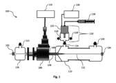
金ナノ粒子を含むアナターゼTiO2薄膜も、図14で示している設定を使用して蒸着された。この設定は、放電後領域に2個の同時注入システムが存在していることを除いて、図1に示している設定に基づいている。一方が、たとえば、TiO2前駆物質(たとえばTEOT、チタン(IV)エトキシド)の霧である第1の化学前駆物質を供給するのに対して、他方は、Au前駆物質(たとえば、HAuCl4.3H2O)の霧である第2の化学前駆物質を供給する。マイクロ波電力は、200Wで設定され、Arプラズマ気体流は、10slmで設定される。
Claims (15)
- 結晶金属酸化物誘導体を基質(112;212)上に蒸着するプラズマ放電後蒸着装置(100;200)であって、
a)基質入口(102;202)を備えている気体源(116;216)と、
b)基質出口(104;204)を備えている放電後蒸着室(110;210)であって、
前記基質入口(102;202)と前記基質出口(104;204)とは、長手方向の中心軸線を定めている放電後蒸着室(110;210)と、
c)前記長手方向の中心軸線上で前記気体源(116;216)と前記蒸着室(110;210)との間に配置されており、プラズマ放電を閉じ込めるように構成されている誘電性チューブ(108;208)と、
を有し、
前記誘電性チューブ(108;208)は、前記誘電性チューブ(108;208)の内側の表面上に配置されている放電区域(136)と、前記長手方向の中心軸線上で中心に配置されている中心区域(138)とを有しており、
前記中心区域(138)は、前記誘電性チューブ(108;208)の内側の表面から1mmと2.5mmとの間の距離に位置しており、
前記誘電性チューブ(108;208)は、プラズマ放電を発生するように構成されている表面波ランチャ(106;206)に囲まれており、
前記プラズマ放電によって前記基質(112;212)を活性化する、プラズマ放電後蒸着装置(100;200)。 - 前記表面波ランチャ(106;206)は、前記中心区域(138)内で150℃以下または150℃、好ましくは100℃未満の温度を提供するように構成されていることを特徴とする、請求項1に記載のプラズマ放電後蒸着装置(100;200)。
- 前記誘電性チューブ(108;208)は、水晶、パイレックス(登録商標)、アルミナ、シリカ、または任意の誘電性材料、優先的には水晶の放電チューブであることを特徴とする、請求項1または2に記載のプラズマ放電後蒸着装置(100;200)。
- 前記表面波ランチャ(106;206)は、300MHzと300GHzとの間の周波数、優先的には2.45GHzの周波数のマイクロ波表面波ランチャであることを特徴とする、請求項1に記載のプラズマ放電後蒸着装置(100;200)。
- 前記放電後蒸着室(110;210)は、前記表面波ランチャ(106;206)から0.5cmと20cmとの間の距離に、優先的には6cmの距離に位置していることを特徴とする、請求項1から4のいずれか1項に記載のプラズマ放電後蒸着装置(100;200)。
- 前記気体源(116;216)は、気体を前記表面波ランチャ(106;206)内に注入するように構成されており、前記気体は、優先的には、アルゴン、ヘリウム、クリプトン、キセノン、窒素、水素、酸素、及び/またはそれらの任意の組み合わせであることを特徴とする、請求項1から5のいずれか1項に記載のプラズマ放電後蒸着装置(100;200)。
- 該装置(100;200)は、装置(100;200)の放電後領域に配置されており、化学前駆物質を基質(112;122)のプラズマ活性化表面上に送達するように構成されており、前記化学前駆物質は、優先的には、結晶金属酸化物誘導体前駆物質、より優先的には、ドーピング用に予備成形されている金属ナノ粒子と混合されている及び/または化学前駆物質と混合されている結晶金属酸化物誘導体前駆物質である、化学前駆物質源(118;218)をさらに有することを特徴とする、請求項1から6のいずれか1項に記載のプラズマ放電後蒸着装置(100;200)。
- 前記化学前駆物質源(118;218)は、化学前駆物質を霧及び/またはエアロゾルの形態で送達するように構成されている微粒化構成(120;220)に接続されており、前記微粒化構成(120;220)は、優先的には超音波システムであることを特徴とする、請求項7に記載のプラズマ放電後蒸着装置(100;200)。
- 前記気体源(116;216)は、金属ナノ粒子前駆物質を前記気体内に送達するように構成されている金属ナノ粒子前駆物質送達システム(248)をさらに有し、前記金属ナノ粒子前駆物質は、より優先的には、銀、パラジウム、プラチナ、または金のナノ粒子前駆物質であることを特徴とする、請求項1から8のいずれか1項に記載のプラズマ放電後蒸着装置(100;200)。
- 該装置は、装置の放電後領域に配置されており、第1の化学前駆物質と第2の化学前駆物質とを基質のプラズマ活性化表面上に送達するように構成されている2個の化学前駆物質源を有し、前記化学前駆物質は、優先的にはチタン(IV)エトキシド及び金三塩酸塩であることを特徴とする、請求項1から9のいずれか1項に記載のプラズマ放電後蒸着装置。
- a)プラズマ活性化基質を生成するように、基質(112;212)をプラズマ放電後蒸着装置内で活性化し、
b)前記プラズマ放電後蒸着装置(100; 200)の放電後領域に配置され、化学前駆物質を基質(112;122)のプラズマ活性化表面上に送達するように構成された化学前駆物質源(118;218)によって、前記プラズマ放電後蒸着装置の放電後領域において前記プラズマ活性化基質に官能基を持たせる、
ステップを有し、
前記化学前駆物質は、結晶金属酸化物誘導体であり、
前記プラズマ放電後蒸着装置は、請求項1から10のいずれか1項に記載のプラズマ放電後蒸着装置(100;200)であることを特徴とする、プラズマ増強化学蒸着方法。 - プラズマ増強化学蒸着は、大気圧及び/または150℃以下または150℃の、好ましくは100℃未満の温度で実施されることを特徴とする、請求項11に記載のプラズマ増強化学蒸着方法。
- 前記基質(112;212)は、熱敏感基質であることを特徴とする、請求項11または12に記載のプラズマ増強化学蒸着方法。
- 前記基質(112;212)は、1次元基質または2次元基質であることを特徴とする、請求項11から13のいずれか1項に記載のプラズマ増強化学蒸着方法。
- 前記結晶金属酸化物誘導体は、優先的には、TiO2、ZnO、WO3、またはドーピングされている結晶金属酸化物誘導体であって、優先的には、ホウ素でドーピングされているTiO2、または金属ナノ粒子の結晶金属酸化物誘導体との混合物であることを特徴とする、請求項11から14のいずれか1項に記載のプラズマ増強化学蒸着方法。
Applications Claiming Priority (3)
| Application Number | Priority Date | Filing Date | Title |
|---|---|---|---|
| LU93221A LU93221B1 (en) | 2016-09-15 | 2016-09-15 | Device for performing atmospheric pressure plasma enhanced chemical vapour deposition at low temperature |
| LU93221 | 2016-09-15 | ||
| PCT/EP2017/073165 WO2018050758A1 (en) | 2016-09-15 | 2017-09-14 | Device for performing atmospheric pressure plasma enhanced chemical vapour deposition at low temperature |
Publications (2)
| Publication Number | Publication Date |
|---|---|
| JP2019533078A JP2019533078A (ja) | 2019-11-14 |
| JP7253255B2 true JP7253255B2 (ja) | 2023-04-06 |
Family
ID=57178453
Family Applications (1)
| Application Number | Title | Priority Date | Filing Date |
|---|---|---|---|
| JP2019512614A Active JP7253255B2 (ja) | 2016-09-15 | 2017-09-14 | 低温で大気圧プラズマ強化化学蒸着を実施する装置 |
Country Status (7)
| Country | Link |
|---|---|
| US (1) | US20190259583A1 (ja) |
| EP (1) | EP3513423B1 (ja) |
| JP (1) | JP7253255B2 (ja) |
| ES (1) | ES2854982T3 (ja) |
| LU (1) | LU93221B1 (ja) |
| PL (1) | PL3513423T3 (ja) |
| WO (1) | WO2018050758A1 (ja) |
Families Citing this family (2)
| Publication number | Priority date | Publication date | Assignee | Title |
|---|---|---|---|---|
| US11251430B2 (en) | 2018-03-05 | 2022-02-15 | The Research Foundation For The State University Of New York | ϵ-VOPO4 cathode for lithium ion batteries |
| TWI754245B (zh) * | 2020-03-17 | 2022-02-01 | 國立陽明交通大學 | 電漿系統及混合電漿與水霧的方法 |
Citations (4)
| Publication number | Priority date | Publication date | Assignee | Title |
|---|---|---|---|---|
| JP2008028231A (ja) | 2006-07-24 | 2008-02-07 | Furukawa Electric Co Ltd:The | 半導体膜形成装置、半導体膜形成方法、及び半導体膜付き線条体 |
| JP2008504442A (ja) | 2004-06-28 | 2008-02-14 | サントル ナショナル ドゥ ラ ルシェルシュ シアンティフィック(セーエヌエールエス) | 電気流体力学、特に後放電噴霧によって、薄膜蒸着する方法及び装置 |
| JP2008073986A (ja) | 2006-09-22 | 2008-04-03 | Dainippon Printing Co Ltd | ガスバリア性積層フィルム |
| JP2011162877A (ja) | 2010-02-08 | 2011-08-25 | Sungkyunkwan Univ Foundation For Corporate Collaboration | グラフィンロールトロールコーティング装置及びこれを用いたグラフィンロールトロールコーティング方法 |
Family Cites Families (4)
| Publication number | Priority date | Publication date | Assignee | Title |
|---|---|---|---|---|
| FR2664294B1 (fr) * | 1990-07-06 | 1992-10-23 | Plasmametal | Procede de metallisation d'une surface. |
| JP3206095B2 (ja) * | 1991-04-12 | 2001-09-04 | 株式会社ブリヂストン | 表面処理方法及びその装置 |
| JP2006324146A (ja) * | 2005-05-19 | 2006-11-30 | Shimada Phys & Chem Ind Co Ltd | 大気圧マイクロ波プラズマ反応装置および方法 |
| US20070212486A1 (en) * | 2005-05-20 | 2007-09-13 | Dinega Dmitry P | Plasma Enhanced Chemical Vapor Deposition of Metal Oxide |
-
2016
- 2016-09-15 LU LU93221A patent/LU93221B1/en active IP Right Grant
-
2017
- 2017-09-14 US US16/333,819 patent/US20190259583A1/en not_active Abandoned
- 2017-09-14 WO PCT/EP2017/073165 patent/WO2018050758A1/en unknown
- 2017-09-14 JP JP2019512614A patent/JP7253255B2/ja active Active
- 2017-09-14 EP EP17768110.3A patent/EP3513423B1/en active Active
- 2017-09-14 PL PL17768110T patent/PL3513423T3/pl unknown
- 2017-09-14 ES ES17768110T patent/ES2854982T3/es active Active
Patent Citations (4)
| Publication number | Priority date | Publication date | Assignee | Title |
|---|---|---|---|---|
| JP2008504442A (ja) | 2004-06-28 | 2008-02-14 | サントル ナショナル ドゥ ラ ルシェルシュ シアンティフィック(セーエヌエールエス) | 電気流体力学、特に後放電噴霧によって、薄膜蒸着する方法及び装置 |
| JP2008028231A (ja) | 2006-07-24 | 2008-02-07 | Furukawa Electric Co Ltd:The | 半導体膜形成装置、半導体膜形成方法、及び半導体膜付き線条体 |
| JP2008073986A (ja) | 2006-09-22 | 2008-04-03 | Dainippon Printing Co Ltd | ガスバリア性積層フィルム |
| JP2011162877A (ja) | 2010-02-08 | 2011-08-25 | Sungkyunkwan Univ Foundation For Corporate Collaboration | グラフィンロールトロールコーティング装置及びこれを用いたグラフィンロールトロールコーティング方法 |
Also Published As
| Publication number | Publication date |
|---|---|
| EP3513423A1 (en) | 2019-07-24 |
| LU93221B1 (en) | 2018-04-11 |
| US20190259583A1 (en) | 2019-08-22 |
| WO2018050758A1 (en) | 2018-03-22 |
| PL3513423T3 (pl) | 2021-07-19 |
| EP3513423B1 (en) | 2020-11-18 |
| JP2019533078A (ja) | 2019-11-14 |
| ES2854982T3 (es) | 2021-09-23 |
Similar Documents
| Publication | Publication Date | Title |
|---|---|---|
| US20220220317A1 (en) | Carbon-nanotube-based composite coating and production method thereof | |
| JP5115522B2 (ja) | 薄膜形成方法 | |
| US20160289826A1 (en) | Method for continuous production of aligned nanostructures on a running substrate and related device | |
| Banerjee et al. | Atmospheric pressure plasma deposition of TiO2: a review | |
| JP7253255B2 (ja) | 低温で大気圧プラズマ強化化学蒸着を実施する装置 | |
| JP2007182605A (ja) | 薄膜形成方法及び薄膜 | |
| US5618580A (en) | Method for producing ceramic fine particles and apparatus used therefor | |
| Jin et al. | Development of CVD Ti-containing films | |
| Quesada-González et al. | Interstitial boron-doped anatase TiO 2 thin-films on optical fibres: atmospheric pressure-plasma enhanced chemical vapour deposition as the key for functional oxide coatings on temperature-sensitive substrates | |
| Karaman et al. | Template assisted synthesis of photocatalytic titanium dioxide nanotubes by hot filament chemical vapor deposition method | |
| AU2013212183A1 (en) | Method for cold gas spraying | |
| CA2802245A1 (en) | Plasma spray method | |
| Mitronika et al. | Hybrid approaches coupling sol–gel and plasma for the deposition of oxide-based nanocomposite thin films: A review | |
| Yuan et al. | The synthesis of C, N-codoped TiO2 hollow spheres by a dual-frequency atmospheric pressure cold plasma jet | |
| Duminica et al. | Pyrosol deposition of anatase TiO2 thin films starting from Ti (OiPr) 4/acetylacetone solutions | |
| García-López et al. | Preparation of photocatalysts by physical methodologies | |
| LU100335B1 (en) | Plasma device for depositing functional composite film comprising crystallized particles embedded in a matrix and method of deposition thereof | |
| JP2003171123A (ja) | 窒素含有酸化亜鉛粉末およびその製造法 | |
| JP6717663B2 (ja) | 膜形成方法 | |
| Beaudette | Nanostructures, nanoparticles, and 2D materials from nonthermal plasmas | |
| Oliveira et al. | SiO x C y H z-TiO 2 Nanocomposite Films Prepared by a Novel PECVD-Sputtering Process | |
| KR101007150B1 (ko) | 정전분무코팅법을 이용한 광촉매 박막 제조 방법 | |
| JP2004285388A (ja) | 薄膜形成装置 | |
| KR100525296B1 (ko) | 화염을 이용한 기상 코팅법에 의해 복합 미세입자를제조하는 방법 | |
| Kim et al. | Uniform coating of TiO2 thin films on particles by rotating cylindrical PCVD reactor |
Legal Events
| Date | Code | Title | Description |
|---|---|---|---|
| A621 | Written request for application examination |
Free format text: JAPANESE INTERMEDIATE CODE: A621 Effective date: 20200820 |
|
| A977 | Report on retrieval |
Free format text: JAPANESE INTERMEDIATE CODE: A971007 Effective date: 20210721 |
|
| A131 | Notification of reasons for refusal |
Free format text: JAPANESE INTERMEDIATE CODE: A131 Effective date: 20210824 |
|
| A601 | Written request for extension of time |
Free format text: JAPANESE INTERMEDIATE CODE: A601 Effective date: 20211124 |
|
| A601 | Written request for extension of time |
Free format text: JAPANESE INTERMEDIATE CODE: A601 Effective date: 20220124 |
|
| A521 | Request for written amendment filed |
Free format text: JAPANESE INTERMEDIATE CODE: A523 Effective date: 20220221 |
|
| A131 | Notification of reasons for refusal |
Free format text: JAPANESE INTERMEDIATE CODE: A131 Effective date: 20220607 |
|
| A601 | Written request for extension of time |
Free format text: JAPANESE INTERMEDIATE CODE: A601 Effective date: 20220906 |
|
| A521 | Request for written amendment filed |
Free format text: JAPANESE INTERMEDIATE CODE: A523 Effective date: 20221107 |
|
| TRDD | Decision of grant or rejection written | ||
| A01 | Written decision to grant a patent or to grant a registration (utility model) |
Free format text: JAPANESE INTERMEDIATE CODE: A01 Effective date: 20230228 |
|
| A61 | First payment of annual fees (during grant procedure) |
Free format text: JAPANESE INTERMEDIATE CODE: A61 Effective date: 20230317 |
|
| R150 | Certificate of patent or registration of utility model |
Ref document number: 7253255 Country of ref document: JP Free format text: JAPANESE INTERMEDIATE CODE: R150 |