JP7183902B2 - Vibration devices, electronic equipment and moving objects - Google Patents
Vibration devices, electronic equipment and moving objects Download PDFInfo
- Publication number
- JP7183902B2 JP7183902B2 JP2019057447A JP2019057447A JP7183902B2 JP 7183902 B2 JP7183902 B2 JP 7183902B2 JP 2019057447 A JP2019057447 A JP 2019057447A JP 2019057447 A JP2019057447 A JP 2019057447A JP 7183902 B2 JP7183902 B2 JP 7183902B2
- Authority
- JP
- Japan
- Prior art keywords
- axis
- vibrating
- vibration
- along
- base
- Prior art date
- Legal status (The legal status is an assumption and is not a legal conclusion. Google has not performed a legal analysis and makes no representation as to the accuracy of the status listed.)
- Active
Links
- 239000000758 substrate Substances 0.000 claims description 113
- 238000001514 detection method Methods 0.000 claims description 42
- 238000006073 displacement reaction Methods 0.000 claims description 26
- 230000005489 elastic deformation Effects 0.000 claims description 8
- 238000005452 bending Methods 0.000 claims description 7
- 239000010453 quartz Substances 0.000 claims description 5
- VYPSYNLAJGMNEJ-UHFFFAOYSA-N silicon dioxide Inorganic materials O=[Si]=O VYPSYNLAJGMNEJ-UHFFFAOYSA-N 0.000 claims description 5
- 239000013078 crystal Substances 0.000 description 15
- 230000000694 effects Effects 0.000 description 9
- WABPQHHGFIMREM-UHFFFAOYSA-N lead(0) Chemical compound [Pb] WABPQHHGFIMREM-UHFFFAOYSA-N 0.000 description 9
- 230000035882 stress Effects 0.000 description 7
- 239000000853 adhesive Substances 0.000 description 6
- 230000001070 adhesive effect Effects 0.000 description 6
- 230000006866 deterioration Effects 0.000 description 6
- 230000000052 comparative effect Effects 0.000 description 4
- 238000013016 damping Methods 0.000 description 4
- 230000006870 function Effects 0.000 description 4
- 239000000463 material Substances 0.000 description 4
- 230000008646 thermal stress Effects 0.000 description 4
- 239000000470 constituent Substances 0.000 description 3
- 238000010586 diagram Methods 0.000 description 3
- 239000002184 metal Substances 0.000 description 3
- 229910052751 metal Inorganic materials 0.000 description 3
- 238000003384 imaging method Methods 0.000 description 2
- 230000003287 optical effect Effects 0.000 description 2
- 241000251468 Actinopterygii Species 0.000 description 1
- WQZGKKKJIJFFOK-GASJEMHNSA-N Glucose Natural products OC[C@H]1OC(O)[C@H](O)[C@@H](O)[C@@H]1O WQZGKKKJIJFFOK-GASJEMHNSA-N 0.000 description 1
- BQCADISMDOOEFD-UHFFFAOYSA-N Silver Chemical compound [Ag] BQCADISMDOOEFD-UHFFFAOYSA-N 0.000 description 1
- NIXOWILDQLNWCW-UHFFFAOYSA-N acrylic acid group Chemical group C(C=C)(=O)O NIXOWILDQLNWCW-UHFFFAOYSA-N 0.000 description 1
- PNEYBMLMFCGWSK-UHFFFAOYSA-N aluminium oxide Inorganic materials [O-2].[O-2].[O-2].[Al+3].[Al+3] PNEYBMLMFCGWSK-UHFFFAOYSA-N 0.000 description 1
- 239000008280 blood Substances 0.000 description 1
- 210000004369 blood Anatomy 0.000 description 1
- 239000000919 ceramic Substances 0.000 description 1
- 239000011231 conductive filler Substances 0.000 description 1
- 230000007423 decrease Effects 0.000 description 1
- 230000000593 degrading effect Effects 0.000 description 1
- 230000007613 environmental effect Effects 0.000 description 1
- 239000000945 filler Substances 0.000 description 1
- 239000008103 glucose Substances 0.000 description 1
- 230000005484 gravity Effects 0.000 description 1
- 229910000833 kovar Inorganic materials 0.000 description 1
- 239000007769 metal material Substances 0.000 description 1
- 238000000034 method Methods 0.000 description 1
- 230000010355 oscillation Effects 0.000 description 1
- 229920001296 polysiloxane Polymers 0.000 description 1
- 230000004044 response Effects 0.000 description 1
- 229910052709 silver Inorganic materials 0.000 description 1
- 239000004332 silver Substances 0.000 description 1
- 238000009736 wetting Methods 0.000 description 1
Images


Classifications
-
- G—PHYSICS
- G01—MEASURING; TESTING
- G01C—MEASURING DISTANCES, LEVELS OR BEARINGS; SURVEYING; NAVIGATION; GYROSCOPIC INSTRUMENTS; PHOTOGRAMMETRY OR VIDEOGRAMMETRY
- G01C19/00—Gyroscopes; Turn-sensitive devices using vibrating masses; Turn-sensitive devices without moving masses; Measuring angular rate using gyroscopic effects
- G01C19/56—Turn-sensitive devices using vibrating masses, e.g. vibratory angular rate sensors based on Coriolis forces
- G01C19/5719—Turn-sensitive devices using vibrating masses, e.g. vibratory angular rate sensors based on Coriolis forces using planar vibrating masses driven in a translation vibration along an axis
- G01C19/5733—Structural details or topology
- G01C19/574—Structural details or topology the devices having two sensing masses in anti-phase motion
-
- G—PHYSICS
- G01—MEASURING; TESTING
- G01C—MEASURING DISTANCES, LEVELS OR BEARINGS; SURVEYING; NAVIGATION; GYROSCOPIC INSTRUMENTS; PHOTOGRAMMETRY OR VIDEOGRAMMETRY
- G01C19/00—Gyroscopes; Turn-sensitive devices using vibrating masses; Turn-sensitive devices without moving masses; Measuring angular rate using gyroscopic effects
- G01C19/56—Turn-sensitive devices using vibrating masses, e.g. vibratory angular rate sensors based on Coriolis forces
- G01C19/5705—Turn-sensitive devices using vibrating masses, e.g. vibratory angular rate sensors based on Coriolis forces using masses driven in reciprocating rotary motion about an axis
-
- H—ELECTRICITY
- H03—ELECTRONIC CIRCUITRY
- H03B—GENERATION OF OSCILLATIONS, DIRECTLY OR BY FREQUENCY-CHANGING, BY CIRCUITS EMPLOYING ACTIVE ELEMENTS WHICH OPERATE IN A NON-SWITCHING MANNER; GENERATION OF NOISE BY SUCH CIRCUITS
- H03B5/00—Generation of oscillations using amplifier with regenerative feedback from output to input
- H03B5/30—Generation of oscillations using amplifier with regenerative feedback from output to input with frequency-determining element being electromechanical resonator
- H03B5/32—Generation of oscillations using amplifier with regenerative feedback from output to input with frequency-determining element being electromechanical resonator being a piezoelectric resonator
-
- G—PHYSICS
- G01—MEASURING; TESTING
- G01P—MEASURING LINEAR OR ANGULAR SPEED, ACCELERATION, DECELERATION, OR SHOCK; INDICATING PRESENCE, ABSENCE, OR DIRECTION, OF MOVEMENT
- G01P3/00—Measuring linear or angular speed; Measuring differences of linear or angular speeds
- G01P3/02—Devices characterised by the use of mechanical means
- G01P3/14—Devices characterised by the use of mechanical means by exciting one or more mechanical resonance systems
Landscapes
- Physics & Mathematics (AREA)
- General Physics & Mathematics (AREA)
- Engineering & Computer Science (AREA)
- Radar, Positioning & Navigation (AREA)
- Remote Sensing (AREA)
- Gyroscopes (AREA)
- Pressure Sensors (AREA)
- Piezo-Electric Or Mechanical Vibrators, Or Delay Or Filter Circuits (AREA)
Description
本発明は、振動デバイス、電子機器および移動体に関するものである。 TECHNICAL FIELD The present invention relates to vibration devices, electronic devices, and moving bodies.
特許文献1に記載されている振動素子は、振動体と、振動体を支持し、パッケージ等に固定される第1支持部および第2支持部と、振動体と第1支持部とを接続している一対の梁部と、振動体と第2支持部とを接続している一対の梁部と、を有する。
The vibrating element described in
しかしながら、上述の振動素子では、振動体の空隙を縫うように梁部を形成しなければならないため、梁部の形状が制約を受ける。そのため、不要振動の周波数設計が制約を受け、不要振動が十分に抑制された振動素子を実現することが困難であった。 However, in the vibrating element described above, since the beams must be formed so as to weave through the gaps of the vibrating body, the shape of the beams is restricted. Therefore, frequency design of unnecessary vibration is restricted, and it has been difficult to realize a vibrating element in which unnecessary vibration is sufficiently suppressed.
本適用例に係る振動デバイスは、互いに直交する3軸をA軸、B軸およびC軸としたとき、
前記A軸および前記B軸に平行な平面に沿って、かつ前記A軸に沿って屈曲振動する振動腕を有する振動素子と、前記振動素子と前記C軸に沿って並んで配置された支持基板と、を備えている振動構造体を有し、
前記支持基板は、前記振動素子を支持している基部と、前記基部を支持している支持部と、前記基部と前記支持部とを接続する梁部と、を有し、
前記振動構造体の前記B軸に沿った振動の共振周波数をf0とし、前記振動素子の駆動周波数をf1としたとき、
f0<f1である。
In the vibrating device according to this application example, when the three mutually orthogonal axes are the A axis, the B axis, and the C axis,
a vibrating element having a vibrating arm that bends and vibrates along a plane parallel to the A-axis and the B-axis and along the A-axis; and a supporting substrate arranged side by side with the vibrating element along the C-axis. and a vibrating structure comprising
The support substrate has a base that supports the vibration element, a support that supports the base, and a beam that connects the base and the support,
When the resonance frequency of vibration of the vibrating structure along the B-axis is f0 and the drive frequency of the vibrating element is f1,
f0<f1.
本適用例に係る振動デバイスでは、前記梁部の前記A軸に沿った弾性変形のばね定数をKaとし、前記梁部の前記B軸に沿った弾性変形のばね定数をKbとしたとき、
Ka>Kbであり、
前記C軸に沿った方向からの平面視で、
前記支持部は、前記振動素子に対して前記A軸に沿った一方側に位置している第1支持部と、前記A軸に沿った他方側に位置している第2支持部と、を有することが好ましい。
In the vibration device according to this application example, when the spring constant of elastic deformation of the beam along the A axis is Ka, and the spring constant of elastic deformation of the beam along the B axis is Kb,
Ka>Kb, and
In a plan view from the direction along the C axis,
The support portion includes a first support portion located on one side along the A axis with respect to the vibration element and a second support portion located on the other side along the A axis. It is preferable to have
本適用例に係る振動デバイスでは、前記C軸に沿った方向からの平面視で、
前記支持部は、前記振動素子に対して前記B軸に沿った一方側に位置している第1支持部と、前記B軸に沿った他方側に位置している第2支持部と、を有することが好ましい。
In the vibration device according to this application example, in a plan view from the direction along the C axis,
The support portion includes a first support portion located on one side along the B axis with respect to the vibration element and a second support portion located on the other side along the B axis. It is preferable to have
本適用例に係る振動デバイスでは、前記振動素子は、
素子基部と、
前記素子基部から前記B軸に沿って両側に向けて延出している検出腕と、
前記素子基部から前記A軸に沿って延出している第1連結腕と、
前記素子基部から前記A軸に沿って前記第1連結腕が延出する方向とは反対側に延出している第2連結腕と、
前記第1連結腕の先端部から前記B軸に沿って両側に向けて延出している前記振動腕と、
前記第2連結腕の先端部から前記B軸に沿って両側に向けて延出し、前記A軸および前記B軸に平行な平面に沿って、かつ前記A軸に沿って屈曲振動する振動腕と、
を有し、
前記素子基部が接合部材を介して前記基部に固定されることが好ましい。
In the vibration device according to this application example, the vibration element includes:
an element base;
detection arms extending from the element base toward both sides along the B-axis;
a first connecting arm extending from the element base along the A-axis;
a second connecting arm extending from the element base along the A-axis in a direction opposite to the direction in which the first connecting arm extends;
the vibrating arms extending from the tip of the first connecting arm toward both sides along the B axis;
a vibrating arm extending from the tip of the second connecting arm toward both sides along the B axis and bending and vibrating along the A axis and a plane parallel to the B axis and along the A axis; ,
has
It is preferable that the element base is fixed to the base via a joining member.
本適用例に係る振動デバイスでは、前記駆動周波数f1における前記振動素子の前記B軸に沿った振動の変位振幅倍率が0.8未満であることが好ましい。 In the vibrating device according to this application example, it is preferable that a displacement amplitude magnification of vibration of the vibrating element along the B-axis at the driving frequency f1 is less than 0.8.
本適用例に係る振動デバイスでは、前記振動素子は、振動基板と、前記振動基板に配置されている電極と、を有し、
前記振動基板および前記支持基板は、同じカット角の水晶基板で構成されていることが好ましい。
In the vibrating device according to this application example, the vibrating element includes a vibrating substrate and electrodes arranged on the vibrating substrate,
It is preferable that the vibration substrate and the support substrate are made of quartz substrates having the same cut angle.
本適用例に係る振動デバイスでは、前記C軸に沿った方向からの平面視で、
前記支持基板と前記振動腕とが重なっていることが好ましい。
In the vibration device according to this application example, in a plan view from the direction along the C axis,
It is preferable that the supporting substrate and the vibrating arms overlap each other.
本適用例に係る振動デバイスでは、前記振動素子は、物理量を検出する物理量センサー素子であることが好ましい。 In the vibrating device according to this application example, it is preferable that the vibrating element is a physical quantity sensor element that detects a physical quantity.
本適用例に係る電子機器は、上述の振動デバイスと、
前記振動デバイスの出力信号に基づいて信号処理を行う信号処理回路と、を備えていることを特徴とする。
An electronic device according to this application example includes the vibration device described above,
and a signal processing circuit that performs signal processing based on the output signal of the vibration device.
本適用例に係る移動体は、上述の振動デバイスと、
前記振動デバイスの出力信号に基づいて信号処理を行う信号処理回路と、を備えていることを特徴とする。
A moving object according to this application example includes the vibration device described above,
and a signal processing circuit that performs signal processing based on the output signal of the vibration device.
以下、本適用例の振動デバイス、電子機器および移動体を添付図面に示す実施形態に基づいて詳細に説明する。 Hereinafter, a vibration device, an electronic device, and a moving body according to this application example will be described in detail based on embodiments shown in the accompanying drawings.
<第1実施形態>
図1は、第1実施形態に係る振動デバイスを示す断面図である。図2は、図1の振動デバイスを示す平面図である。図3は、図1の振動デバイスが有する振動素子を示す平面図である。図4および図5は、図3の振動素子の駆動を説明する模式図である。図6は、図1に示す振動デバイスが有する支持基板を示す平面図である。図7は、周波数比f1/fdと、駆動周波数f1における不要振動の変位振幅倍率(gain)との関係を示すグラフである。図8は、周波数比f1/fd=1のときの、f0/f1と、駆動周波数f1における不要振動の変位振幅倍率(gain)との関係を示すグラフである。なお、説明の便宜上、図1ないし図6には、互いに直交する3軸であるA軸、B軸およびC軸を示している。また、以下では、各軸の矢印先端側を「プラス側」とも言い、反対側を「マイナス側」とも言う。また、C軸のプラス側を「上」とも言い、マイナス側を「下」とも言う。また、C軸に沿った方向からの平面視を、単に「平面視」とも言う。
<First embodiment>
FIG. 1 is a cross-sectional view showing the vibration device according to the first embodiment. 2 is a plan view showing the vibration device of FIG. 1. FIG. 3 is a plan view showing a vibration element included in the vibration device of FIG. 1. FIG. 4 and 5 are schematic diagrams for explaining the driving of the vibrating element of FIG. 3. FIG. 6 is a plan view showing a support substrate of the vibrating device shown in FIG. 1. FIG. FIG. 7 is a graph showing the relationship between the frequency ratio f1/fd and the displacement amplitude magnification (gain) of unwanted vibration at the drive frequency f1. FIG. 8 is a graph showing the relationship between f0/f1 and the displacement amplitude magnification (gain) of unwanted vibration at the drive frequency f1 when the frequency ratio f1/fd=1. For convenience of explanation, FIG. 1 to FIG. 6 show three mutually perpendicular axes, the A-axis, the B-axis and the C-axis. Also, hereinafter, the arrow tip side of each axis is also called the "plus side", and the opposite side is also called the "minus side". Also, the positive side of the C-axis is also called "upper" and the negative side is also called "lower". A planar view from the direction along the C-axis is also simply referred to as a “planar view”.
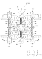
図1に示す振動デバイス1は、C軸を検出軸とする角速度ωcを検出する物理量センサーである。振動デバイス1を物理量センサーとすることにより、振動デバイス1を幅広い電子機器に搭載することができ、利便性の高い振動デバイス1となる。このような振動デバイス1は、パッケージ2と、パッケージ2に収納されている回路素子3、支持基板4および振動素子6と、を有している。
A
パッケージ2は、上面に開口する凹部211を備えるベース21と、凹部211の開口を塞ぐようにベース21の上面に接合部材23を介して接合されているリッド22と、を有する。パッケージ2の内側には凹部211によって内部空間Sが形成され、内部空間Sに回路素子3、支持基板4および振動素子6が収容されている。例えば、ベース21は、アルミナ等のセラミックスで構成することができ、リッド22は、コバール等の金属材料で構成することができる。ただし、ベース21およびリッド22の構成材料としては、それぞれ、特に限定されない。
The
収納空間Sは、気密であり、減圧状態、好ましくは、より真空に近い状態となっている。これにより、振動素子6の振動特性が向上する。ただし、収納空間Sの雰囲気は、特に限定されず、例えば、大気圧状態、加圧状態となっていてもよい。
The storage space S is airtight and is in a decompressed state, preferably in a state closer to a vacuum. Thereby, the vibration characteristics of the vibrating
また、凹部211は、複数の凹部で構成され、ベース21の上面に開口している凹部211aと、凹部211aの底面に開口し、凹部211aよりも開口幅が小さい凹部211bと、凹部211bの底面に開口し、凹部211bよりも開口幅が小さい凹部211cと、を有する。そして、凹部211aの底面に、振動素子6を支持した状態で支持基板4が固定され、凹部211cの底面に、回路素子3が固定されている。
The recessed
また、図2に示すように、内部空間Sにおいて、振動素子6、支持基板4および回路素子3は、平面視で互いに重なって配置されている。言い換えると、振動素子6、支持基板4および回路素子3は、C軸に沿って並んで配置されている。これにより、パッケージ2のA軸およびB軸に沿った方向への平面積の広がりを抑制でき、振動デバイス1の小型化を図ることができる。また、支持基板4は、振動素子6と回路素子3との間に位置し、振動素子6を下側すなわちC軸マイナス側から支えるように支持している。
Further, as shown in FIG. 2, in the internal space S, the
また、図1および図2に示すように、凹部211aの底面には複数の内部端子241が配置され、凹部211bの底面には複数の内部端子242が配置され、ベース21の下面には複数の外部端子243が配置されている。これら内部端子241、242および外部端子243は、ベース21内に形成されている図示しない配線を介して電気的に接続されている。また、内部端子241は、導電性の接合部材B1、B2および支持基板4を介して振動素子6と電気的に接続され、内部端子242は、ボンディングワイヤーBWを介して回路素子3と電気的に接続されている。
1 and 2, a plurality of
振動素子6は、物理量センサー素子として、C軸を検出軸とする角速度ωcを検出することのできる角速度センサー素子である。図3に示すように、振動素子6は、振動基板7と、振動基板7の表面に配置されている電極8と、を有する。また、振動基板7は、Zカットの水晶基板で構成され、素子の中央部に位置する素子基部70と、素子基部70からB軸に沿って両側に向けて延出している検出腕71、72と、素子基部70からA軸に沿って延出している第1連結腕73と、素子基部70からA軸に沿って第1連結腕73が延出している方向とは反対側に延出している第2連結腕74と、第1連結腕73の先端部からB軸に沿って両側に向けて延出している振動腕としての駆動腕75、76と、第2連結腕74の先端部からB軸に沿って両側に向けて延出している振動腕としての駆動腕77、78と、を有する。なお、Zカットの水晶基板は、水晶の結晶軸である電気軸としてのX軸および機械軸としてのY軸で規定されるX-Y平面に広がりを有し、光軸としてのZ軸に沿った方向に厚みを有している。
The
また、各検出腕71、72は、その先端部に、基端側の部分よりも幅広の幅広部711、721を有する。また、各駆動腕75、76、77、78は、その先端部に、基端側の部分よりも幅広の幅広部751、761、771、781を有する。
In addition, each of the
また、電極8は、駆動信号電極81と、駆動接地電極82と、第1検出信号電極83と、第1検出接地電極84と、第2検出信号電極85と、第2検出接地電極86と、を有する。駆動信号電極81は、駆動腕75、76の上下面と駆動腕77、78の両側面とに配置されている。一方、駆動接地電極82は、駆動腕75、76の両側面と駆動腕77、78の上下面とに配置されている。また、第1検出信号電極83は、検出腕71の上下面に配置され、第1検出接地電極84は、検出腕71の両側面に配置されている。一方、第2検出信号電極85は、検出腕72の上下面に配置され、第2検出接地電極86は、検出腕72の両側面に配置されている。
The
また、これら電極81~86は、それぞれ、素子基部70の下面まで引き回されている。そのため、素子基部70の下面には、駆動信号電極81と電気的に接続されている端子701と、駆動接地電極82と電気的に接続されている端子702と、第1検出信号電極83と電気的に接続されている端子703と、第1検出接地電極84と電気的に接続されている端子704と、第2検出信号電極85と電気的に接続されている端子705と、第2検出接地電極86と電気的に接続されている端子706と、が配置されている。
Further, these
また、図3に示すように、振動素子6は、駆動腕75~78の幅広部751~781にも電極8が配置されている。振動デバイス1では、リッド22をベース21に接合する前に、C軸プラス側から幅広部751~781上の電極8にレーザー光を照射し、電極8の少なくとも一部を除去することにより、駆動腕75~78の質量を減少させ、振動素子6の振動バランスや駆動周波数を調整することができる。以下、この工程を「駆動周波数調整工程」とも言う。
In addition, as shown in FIG. 3, the vibrating
このような振動素子6は、次のようにして角速度ωcを検出する。まず、駆動信号電極81および駆動接地電極82間に駆動信号を印加すると、駆動腕75~78が、図4に示すように、A軸およびB軸に平行な平面内に沿って、かつA軸に沿って屈曲振動する。以下、この駆動モードを駆動振動モードと言う。そして、駆動振動モードで駆動している状態で、振動素子6に角速度ωcが加わると、図5に示す検出振動モードが新たに励振される。検出振動モードでは、駆動腕75~78にコリオリの力が作用して矢印Dに示す方向の振動が励振され、この振動に呼応して、検出腕71、72が矢印Eに示す方向に屈曲振動する。このような検出振動モードによって検出腕71に発生した電荷を第1検出信号電極83および第1検出接地電極84の間から第1検出信号として取り出し、検出腕72に発生した電荷を第2検出信号電極85および第2検出接地電極86の間から第2検出信号として取り出し、これら第1、第2検出信号に基づいて角速度ωcを検出することができる。
Such a
図1に示すように、回路素子3は、凹部211cの底面に固定されている。また、回路素子3には、振動素子6を駆動し、振動素子6に加わった角速度ωcを検出する駆動回路および検出回路が含まれている。ただし、回路素子3としては、特に限定されず、例えば、温度補償回路等、他の回路が含まれていてもよい。
As shown in FIG. 1, the
図2に示すように、支持基板4は、基部40と、基部40を支持し、基部40のA軸に沿って両側に分かれて配置されている第1支持部411および第2支持部412を備える支持部41と、基部40と第1支持部411とを接続している一対の梁部42、43と、基部40と第2支持部412とを接続している一対の梁部44、45と、を有する。
As shown in FIG. 2, the
そして、基部40に導電性の接合部材B2を介して振動素子6の素子基部70が固定されており、第1支持部411および第2支持部412がそれぞれ接合部材B1を介して凹部211aの底面に固定されている。つまり、振動素子6は、支持基板4を介してベース21に固定されている。このように、振動素子6とベース21との間に支持基板4を介在させることにより、支持基板4によってベース21から伝わる応力を吸収、緩和することができ、当該応力が振動素子6に伝わり難くなる。そのため、振動素子6の振動特性の低下や変動を効果的に抑制することができる。
The
特に、本実施形態では、平面視で、第1、第2支持部411、412がそれぞれ振動素子6の外側に位置している。具体的には、振動素子6のA軸プラス側に第1支持部411が位置し、A軸マイナス側に第2支持部412が位置している。これにより、第1、第2支持部411、412を、振動素子6を間に挟んで互いに十分に離間させて配置することができるため、支持基板4によって振動素子6をより安定した姿勢で支持することができる。そのため、振動素子6の振動特性が向上する。
In particular, in this embodiment, the first and
なお、接合部材B1、B2としては、導電性と接合性とを兼ね備えていれば、特に限定されず、例えば、金バンプ、銀バンプ、銅バンプ、はんだバンプ等の各種金属バンプ、ポリイミド系、エポキシ系、シリコーン系、アクリル系の各種接着剤に銀フィラー等の導電性フィラーを分散させた導電性接着剤等を用いることができる。接合部材B1、B2として前者の金属バンプを用いると、接合部材B1、B2からのガスの発生を抑制でき、内部空間Sの環境変化、特に圧力の上昇を効果的に抑制することができる。一方、接合部材B1、B2として後者の導電性接着剤を用いると、接合部材B1、B2が比較的柔らかくなり、接合部材B1、B2においても前述の応力を吸収、緩和することができる。 The bonding members B1 and B2 are not particularly limited as long as they have both conductivity and bonding properties. A conductive adhesive obtained by dispersing a conductive filler such as a silver filler in various types of adhesives such as silicone-based, acrylic-based, etc. can be used. When the former metal bumps are used as the bonding members B1 and B2, generation of gas from the bonding members B1 and B2 can be suppressed, and environmental changes in the internal space S, particularly pressure increases, can be effectively suppressed. On the other hand, when the latter conductive adhesive is used as the joint members B1 and B2, the joint members B1 and B2 become relatively soft, and the aforementioned stress can be absorbed and relaxed in the joint members B1 and B2 as well.
本実施形態では、接合部材B1として導電性接着剤を用いており、接合部材B2として金属バンプを用いている。異種の材料である支持基板4とベース21とを接合する接合部材B1として導電性接着剤を用いることにより、これらの間の熱膨張係数の差に起因して生じる熱応力を接合部材B1によって効果的に吸収、緩和することができる。一方、支持基板4と振動素子6とは、比較的狭い領域に配置されている6つの接合部材B2で接合されているため、接合部材B2として金属バンプを用いることにより、導電性接着剤のような濡れ広がりが抑制され、接合部材B2同士の接触を効果的に抑制することができる。
In this embodiment, a conductive adhesive is used as the bonding member B1, and a metal bump is used as the bonding member B2. By using a conductive adhesive as the bonding member B1 for bonding the
図3に示すように、梁部42、43、44、45は、それぞれ、その途中にS字状に蛇行した屈曲部421、431、441、451を有し、A軸方向およびB軸方向に弾性変形し易い形状となっている。そのため、梁部42~45によって、ベース21から伝わる応力をより効果的に吸収、緩和することができる。ただし、梁部42~45の形状は、それぞれ、特に限定されず、例えば、屈曲部421~451を省略してストレート状としてもよい。また、梁部42~45は、少なくとも1つが他と異なる形状となっていてもよい。
As shown in FIG. 3, the
また、平面視で、振動素子6の駆動腕75が梁部42と重なっており、駆動腕76が梁部43と重なっており、駆動腕77が梁部44と重なっており、駆動腕78が梁部45と重なっている。そのため、衝撃等によって駆動腕75~78がC軸方向に撓んだ際、駆動腕75~78が梁部42~45と接触し、それ以上の過度な撓みが抑制される。すなわち、梁部42~45が駆動腕75~78のC軸方向への過度な変形を抑制するストッパーとして機能する。これにより、振動素子6の破損を抑制することができる。特に、梁部42~45は、支持基板4の中でも柔らかい部位であるため、駆動腕75~78を梁部42~45に接触させることにより、接触時の衝撃を和らげることもできる。また、本実施形態では、駆動腕75~78の先端部すなわち幅広部751~781と梁部42~45とが重なっているため、駆動腕75~78のC軸方向への過度な変形をより効果的に抑制することができる。
In a plan view, the
ただし、これに限定されず、例えば、基部40や第1、第2支持部411、412が駆動腕75~78と重なっていてもよいし、基部40、第1、第2支持部411、412および梁部42~45のいずれも駆動腕75~78と重なっていなくてもよい。
However, it is not limited to this, and for example, the
このような支持基板4は、水晶基板で構成されている。このように、支持基板4を振動基板7と同様に水晶基板で構成することにより、支持基板4と振動基板7との熱膨張係数を等しくすることができる。そのため、支持基板4と振動基板7との間には、互いの熱膨張係数差に起因する熱応力が実質的に生じず、振動素子6がより応力を受け難くなる。そのため、振動素子6の振動特性の低下や変動をより効果的に抑制することができる。
Such a
特に、支持基板4は、振動素子6が有する振動基板7と同じカット角の水晶基板で構成されている。本実施形態では、振動基板7がZカット水晶基板で構成されているため、支持基板4もZカット水晶基板で構成されている。また、支持基板4の結晶軸の向きは、振動基板7の結晶軸の向きと一致している。すなわち、支持基板4と振動基板7とで互いにX軸に沿う方向が一致し、互いにY軸に沿う方向が一致し、互いにZ軸に沿う方向が一致している。水晶は、X軸に沿う方向、Y軸に沿う方向およびZ軸に沿う方向のそれぞれで熱膨張係数が異なるため、支持基板4と振動基板7とを同じカット角とし、互いの結晶軸の向きを揃えることにより、支持基板4と振動基板7との間で前述の熱応力がより生じ難くなる。そのため、振動素子6がさらに応力を受け難くなり、その振動特性の低下や変動をさらに効果的に抑制することができる。
In particular, the
なお、支持基板4としては、これに限定されず、例えば、振動基板7と同じカット角であるが、結晶軸の方向が振動基板7とは異なっていてもよい。また、支持基板4は、振動基板7と異なるカット角の水晶基板から形成されていてもよい。また、支持基板4は、水晶基板から形成されていなくてもよい。この場合、支持基板4の構成材料は、水晶との熱膨張係数の差が、水晶とベース21の構成材料との熱膨張係数差よりも小さい材料であることが好ましい。
Note that the
また、支持基板4には、振動素子6と内部端子241とを電気的に接続する配線5が配置されている。図6に示すように、配線5は、基部40に配置されている端子511、521、531、541、551、561と、第1支持部411に配置されている端子512、532、542と、第2支持部412に配置されている端子522、552、562と、を有する。また、配線5は、梁部42を通って端子511と端子512を接続する引出配線513と、梁部44を通って端子521と端子522とを接続する引出配線523と、梁部43を通って端子531と端子532とを接続する引出配線533と、梁部42、43を通って端子541と端子542とを接続する引出配線543と、梁部45を通って端子551と端子552とを接続する引出配線553と、梁部44、45を通って端子561と端子562とを接続する引出配線563と、を有する。
Wiring 5 for electrically connecting the vibrating
そして、図示しないが、基部40に配置されている端子511~561は、接合部材B2を介して、振動素子6の素子基部70に配置されている端子701~706と電気的に接続されており、第1、第2支持部411、412に配置されている端子512~562は、接合部材B1を介して、内部端子241と電気的に接続されている。これにより、振動素子6と回路素子3とが電気的に接続される。
Although not shown, the
以上、振動デバイス1の構成について簡単に説明した。ここで、前述した振動素子6では、例えば、振動基板7の駆動周波数調整工程によって駆動腕75~78の重量バランスが十分に調整されず、振動素子6の重心が素子の中心からずれてしまうと、駆動振動モード時に振動素子6がB軸に沿って振動する不要振動(以下、単に「不要振動」と言う。)が生じる。この不要振動が生じると振動素子6の振動漏れが大きくなり、その分、Q値が低下して振動素子6の振動特性が低下する。
The configuration of the
そこで、振動デバイス1では、振動素子6を支持している支持基板4で振動素子6の不要振動を減衰し、振動素子6の振動特性の低下を抑制する構成となっている。以下、このことについて詳細に説明する。なお、以下では、振動素子6と支持基板4とからなる構造体を「振動構造体10」とも言う。振動構造体10は、基部40および振動素子6を含む質量部と、4つの梁部42~45を含むばね部と、からなる振動系100を有する。
Therefore, in the vibrating
前述したように、振動デバイス1では、振動素子6を支持する支持基板4を振動素子6とは別体で構成し、しかも、支持基板4と振動素子6とをC軸に沿って重ねて配置している。これにより、振動素子6に邪魔されることなく、支持基板4を自由に設計することができる。支持基板4の設計自由度が増すことにより、その設計がより好適なものとなり、より効果的に振動素子6の不要振動を抑制することができる。
As described above, in the vibrating
振動構造体10すなわち振動系100のB軸に沿った振動の共振周波数をf0とし、駆動振動モードにおける振動素子6単体の駆動周波数をf1としたとき、本実施形態の振動デバイス1は、f0<f1の関係を満たす。振動素子6の不要振動は、駆動振動モードにおける駆動腕75~78の振動に起因して生じるため、その周波数は、駆動周波数f1と実質的に等しい。したがって、f0<f1とすることにより、実質的にf1である不要振動の周波数と共振周波数f0との間に差が生じ、言い換えると、不要振動の周波数が共振周波数f0からずれ、不要振動に呼応した振動系100の共振を抑制することができる。そのため、支持基板4によって振動素子6の不要振動を効果的に減衰させることができる。
When the resonance frequency of the vibration of the vibrating
ここで、共振周波数f0と駆動周波数f1との間に差を生じさせるためなら、f0>f1であってもよい。しかしながら、f0>f1とするには、振動系100の前記質量部を軽くするか、振動系100の前記ばね部のばね定数を大きくする必要がある。そして、前者の場合、例えば、振動素子6のサイズを小さくすることにより対応可能であるが、振動素子6のサイズを小さくすれば、その分、振動素子6の振動特性が低下する。一方、後者の場合、梁部42~45を硬くすることにより対応可能であるが、梁部42~45を硬くすれば、その分、パッケージ2からの応力が支持基板4を伝って振動素子6に伝わり易くなる。このように、f0>f1では、他の要因によって振動素子6の振動特性の低下を招いてしまう。これに対して、本実施形態のように、f0<f1とすれば、そのような問題が生じず、より効果的に、振動素子6の振動特性の低下を抑制することができる。
Here, f0>f1 may be satisfied in order to generate a difference between the resonance frequency f0 and the drive frequency f1. However, in order to satisfy f0>f1, it is necessary to lighten the mass portion of the
特に、本実施形態では、梁部42~45をB軸よりもA軸に沿って長く形成させており、これにより、各梁部42~45は、A軸に沿った弾性変形よりもB軸に沿って弾性変形し易くなっている。つまり、振動系100のばね部では、A軸に沿った弾性変形のばね定数をKaとし、B軸に沿った弾性変形のばね定数をKbとしたとき、Ka>Kbである。これにより、共振周波数f0を効果的に下げることができ、共振周波数f0と駆動周波数f1の差f1-f0をより大きくすることができる。したがって、支持基板4による不要振動の減衰効果がより向上する。なお、ばね定数Ka、Kbは、0.2≦Kb/Ka≦0.8であることが好ましく、0.3≦Kb/Ka≦0.7であることがより好ましく、0.4≦Kb/Ka≦0.6であることがさらに好ましい。これにより、梁部42~45の機械的強度を確保しつつ、ばね定数Kbを十分に小さくすることができる。そのため、支持基板4による不要振動の減衰効果がさらに向上する。ただし、これに限定されず、Ka≦Kbであってもよい。
In particular, in this embodiment, the
次に、図7に、振動素子6のB軸に沿った振動である不要振動の周波数をfdとしたときのf1/fdと、駆動周波数f1における振動素子6のB軸に沿った振動の変位振幅倍率(gain)との関係を示す。なお、「変位振幅」とは、振動時の寸法変位の最大幅であり、「変位振幅倍率」とは、f1/fdを0.01としたときの変位振幅に対する変位振幅の倍率である。このグラフ中の曲線Q1は、本実施形態の振動構造体10であり、曲線Q2は、後述する第2実施形態の振動構造体10であり、曲線Q3は、従来技術で挙げた特開2017-194485号公報に記載されている比較例としての振動素子である。
Next, FIG. 7 shows f1/fd, where fd is the frequency of unwanted vibration that is vibration along the B axis of the
前述したように、不要振動の周波数fdは、駆動周波数f1と実質的に等しいため、図7中のf1/fd=1について比較すれば、本実施形態の振動構造体10の変位振幅倍率(gain)が最も小さく、次に、後述する第2実施形態の振動構造体10の変位振幅倍率(gain)が小さく、比較例としての振動素子の変位振幅倍率(gain)が最も大きいことが分かる。変位振幅倍率(gain)が小さい程、振動系100における質量部すなわち振動素子6のB軸方向への振幅が小さいことを意味するため、本実施形態の振動構造体10によれば、振動素子6の不要振動をより効果的に減衰させることができる。
As described above, since the frequency fd of the unwanted vibration is substantially equal to the drive frequency f1, the displacement amplitude magnification (gain ) is the smallest, the displacement amplitude magnification (gain) of the
また、図8に、f1/fd=1のときの、振動系100のB軸に沿った振動の共振周波数f0と駆動周波数f1の比であるf0/f1と、駆動周波数f1における振動素子6のB軸に沿った振動の変位振幅倍率(gain)との関係を示す。この図から分かるように、f0/f1が小さくなる程、すなわち、共振周波数f0と駆動周波数f1の差:f1-f0が大きくなる程、変位振幅倍率(gain)が小さくなる。そして、本実施形態では、変位振幅倍率(gain)が0.8未満である。比較例として挙げた振動素子の変位振幅倍率(gain)が0.8であるため、少なくとも0.8未満であれば、比較例に対して優れた不要振動減衰効果を発揮することができる。なお、変位振幅倍率(gain)は、0.6未満であることが好ましく、0.4未満であることがより好ましく、0.2未満であることがさらに好ましい。これにより、不要振動減衰効果をより顕著に発揮することができる。
FIG. 8 shows f0/f1, which is the ratio between the resonance frequency f0 of the vibration of the
なお、図8から、変位振幅倍率を0.8未満とするには、f0/f1を0.7未満とすればよく、変位振幅倍率を0.6未満とするには、f0/f1を0.65未満とすればよく、変位振幅倍率を0.4未満とするには、f0/f1を0.55未満とすればよく、変位振幅倍率を0.2未満とするには、f0/f1を0.4未満とすればよいことが分かる。つまり、f0/f1は、0.7未満であることが好ましく、0.65未満であることがより好ましく、0.55未満であることがさらに好ましく、0.4未満であることがますます好ましい。 From FIG. 8, f0/f1 should be less than 0.7 in order to make the displacement amplitude magnification less than 0.8, and f0/f1 should be 0 in order to make the displacement amplitude magnification less than 0.6. 0.65, f0/f1 should be less than 0.55 to make the displacement amplitude ratio less than 0.4, and f0/f1 to make the displacement amplitude ratio less than 0.2. is less than 0.4. That is, f0/f1 is preferably less than 0.7, more preferably less than 0.65, even more preferably less than 0.55, and even more preferably less than 0.4. .
以上、振動デバイス1について説明した。振動デバイス1は、前述したように、互いに直交する3軸をA軸、B軸およびC軸としたとき、A軸およびB軸に平行な平面に沿って、かつA軸に沿って屈曲振動する振動腕としての駆動腕75、76、77、78を有する振動素子6と、振動素子6とC軸に沿って並んで配置された支持基板4と、を備えている振動構造体10を有する。また、支持基板4は、振動素子6を支持している基部40と、基部40を支持している支持部41と、基部40と支持部41とを接続する梁部42、43、44、45と、を有する。そして、振動構造体10のB軸に沿った振動の共振周波数をf0とし、振動素子6の駆動周波数をf1としたとき、f0<f1である。このように、f0<f1とすることにより、実質的にf1である不要振動の周波数と共振周波数f0とに差が生じ、不要振動による振動系100の共振を抑制することができる。そのため、支持基板4によって振動素子6の不要振動を効果的に減衰させることができる。
The
また、前述したように、梁部42、43、44、45のA軸に沿った弾性変形のばね定数をKaとし、梁部42、43、44、45のB軸に沿った弾性変形のばね定数をKbとしたとき、Ka>Kbである。また、C軸に沿った方向からの平面視で、支持部41は、振動素子6に対してA軸に沿った一方側、本実施形態ではプラス側に位置している第1支持部411と、A軸に沿った他方側、本実施形態ではマイナス側に位置している第2支持部412と、を有する。このように、第1、第2支持部411、412を振動素子6の両側に配置することにより、振動素子6を安定した姿勢で支持することができる。そのため、振動素子6の振動特性が安定する。また、第1、第2支持部411、412をA軸に沿って並べて配置することにより、基部40と第1、第2支持部411、412とを接続する梁部42、43、44、45をB軸よりもA軸に沿って長く形成させ易くなり、Ka>Kbの関係を満たし易くなる。そのため、支持基板4の設計自由度が向上する。
Further, as described above, the spring constant of elastic deformation along the A-axis of the
また、前述したように、振動素子6は、素子基部70と、素子基部70からB軸に沿って両側に向けて延出している検出腕71、72と、素子基部70からA軸に沿って延出している第1連結腕73と、素子基部70からA軸に沿って第1連結腕73が延出する方向とは反対側に延出している第2連結腕74と、第1連結腕73の先端部からB軸に沿って両側に向けて延出している振動腕としての駆動腕75、76と、第2連結腕74の先端部からB軸に沿って両側に向けて延出している振動腕としての駆動腕77、78と、を有しており、素子基部70が接合部材B2を介して基部40に固定されている。これにより、物理量を検出する物理量センサー素子としての振動素子6の不要振動をより効果的に減衰させることができ、高精度の振動デバイス1を実現することができる。
As described above, the
また、前述したように、駆動周波数f1における振動素子6のB軸に沿った振動の変位振幅倍率(gain)が0.8未満である。これにより、支持基板4によって、振動素子6の不要振動をより効果的に減衰させることができる。
Further, as described above, the displacement amplitude magnification (gain) of the vibration of the vibrating
また、前述したように、振動素子6は、振動基板7と、振動基板7に配置されている電極8と、を有する。そして、振動基板7および支持基板4は、同じカット角の水晶基板で構成されている。これにより、支持基板4と振動基板7との熱膨張係数を等しくすることができる。そのため、支持基板4と振動基板7との間には、互いの熱膨張係数差に起因する熱応力が実質的に生じず、振動素子6がより応力を受け難くなる。そのため、振動素子6の振動特性の低下や変動をより効果的に抑制することができる。
Further, as described above, the vibrating
また、前述したように、C軸に沿った方向からの平面視で、支持基板4と駆動腕75、76、77、78とが重なっている。そのため、支持基板4が駆動腕75~78のC軸方向への過度な変形を抑制するストッパーとして機能し、振動素子6の破損を効果的に抑制することができる。
Further, as described above, the
また、前述したように、振動素子6は、物理量を検出する物理量センサー素子である。特に、本実施形態では、振動素子6は、角速度ωcを検出する角速度センサー素子である。これにより、振動デバイス1を幅広い電子機器に搭載することができ、利便性の高い振動デバイス1となる。
Also, as described above, the
なお、以上のような第1実施形態では、支持基板4は、振動素子6と回路素子3との間に位置し、振動素子6を下側すなわちC軸マイナス側から支えるように支持していたが、振動素子6は、支持基板4と回路素子3との間に位置し、支持基板4が、振動素子6を上側すなわちC軸プラス側から支えるように支持してもよい。また、第1実施形態では、支持基板4は、接合部材B1を介してベース21の凹部211aの底面に固定されていたが、支持基板4は、接合部材を介して回路素子3に固定されていてもよい。
In the first embodiment as described above, the supporting
<第2実施形態>
図9は、第2実施形態の振動デバイスを示す平面図である。
<Second embodiment>
FIG. 9 is a plan view showing the vibration device of the second embodiment.
本実施形態は、振動素子6の向きが異なること以外は、前述した第1実施形態と同様である。なお、以下の説明では、本実施形態に関し、前述した実施形態との相違点を中心に説明し、同様の事項に関してはその説明を省略する。また、図9において、前述した実施形態と同様の構成については、同一符号を付している。
This embodiment is the same as the above-described first embodiment except that the orientation of the
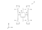
図9示すように、本実施形態の支持基板4では、振動素子6以外の各部分、すなわち、パッケージ2、支持基板4および回路素子3が前述した第1実施形態からC軸まわりに90°回転して配置されている。すなわち、支持基板4は、基部40と、基部40を支持し、基部40のB軸に沿って両側に分かれて配置されている第1支持部411および第2支持部412を備える支持部41と、基部40と第1支持部411とを接続している一対の梁部42、43と、基部40と第2支持部412とを接続している一対の梁部44、45と、を有する。そして、基部40に導電性の接合部材B2を介して振動素子6の素子基部70が固定されており、第1支持部411および第2支持部412がそれぞれ接合部材B1を介して凹部211aの底面に固定されている。このような構成によっても、前述した図7中の曲線Q2に示すように、支持基板4によって振動素子6の不要振動を効果的に減衰させることができる。なお、支持基板4は、結晶軸の向きについてはC軸まわりに回転しておらず、前述した第1実施形態のままである。
As shown in FIG. 9, in the
このような、本実施形態の振動デバイス1によれば、支持基板4によって振動素子6の不要振動を効果的に減衰させることができるとともに、第1、第2支持部411、412を振動素子6の両側に配置することにより、振動素子6を安定した姿勢で支持することができる。そのため、振動素子6の振動特性が安定する。
According to the
<第3実施形態>
図10は、第3実施形態の振動デバイスが有する支持基板を示す平面図である。
<Third Embodiment>
FIG. 10 is a plan view showing a support substrate included in the vibrating device of the third embodiment.
本実施形態は、支持基板4の構成が異なること以外は、前述した第1実施形態と同様である。なお、以下の説明では、本実施形態に関し、前述した実施形態との相違点を中心に説明し、同様の事項に関してはその説明を省略する。また、図10において、前述した実施形態と同様の構成については、同一符号を付している。
This embodiment is the same as the first embodiment described above, except that the configuration of the
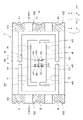
図10に示すように、本実施形態の支持基板4は、ジンバル形状となっている。すなわち、支持基板4は、中央部に位置し、接合部材B2を介して振動素子6が固定されている基部46と、基部46を囲み、基部46を支持すると共に接合部材B1を介して凹部211aの底面に固定されている支持部47と、基部46と支持部47との間に位置し、これらを接続する梁部48と、を有する。
As shown in FIG. 10, the
また、梁部48は、基部46と支持部47との間に位置し、基部46を囲む枠状の枠部481と、基部46と枠部481とを接続する第1梁部482と、支持部47と枠部481とを接続する第2梁部483と、を有する。第1梁部482は、B軸に沿った方向の中央において基部46と枠部481とを接続しており、その中心軸J2がA軸に沿っている。一方、第2梁部483は、A軸に沿った方向の中央において支持部47と枠部481とを接続しており、その中心軸J1がB軸に沿っている。つまり、中心軸J1、J2は、直交しており、その交点は、支持基板4の中心O4とほぼ一致している。ただし、中心軸J1、J2は、0°超90°未満の角度で交わっていてもよいし、これらの交点が中心O4からずれていてもよい。
The
また、支持部47は、矩形の枠状をなし、平面視で、振動素子6に対してA軸プラス側に位置する第1支持部471と、A軸マイナス側に位置する第2支持部472と、を有する。そして、第1支持部471および第2支持部472がそれぞれ接合部材B1を介して凹部211aの底面に固定されている。
In addition, the
このような構成によっても、前述した第1実施形態と同様の作用効果を発揮することができる。なお、本実施形態では、支持部47が枠状をなしているが、これに限定されず、例えば、周方向の一部が欠損して、C字状となっていてもよい。枠部481についても同様である。
Such a configuration can also exhibit the same effects as the first embodiment described above. Although the supporting
<第4実施形態>
図11は、第4実施形態のパーソナルコンピューターを示す斜視図である。
<Fourth Embodiment>
FIG. 11 is a perspective view showing the personal computer of the fourth embodiment.
図11に示す電子機器としてのパーソナルコンピューター1100は、キーボード1102を備えた本体部1104と、表示部1108を備えた表示ユニット1106と、により構成され、表示ユニット1106は、本体部1104に対しヒンジ構造部を介して回動可能に支持されている。また、パーソナルコンピューター1100には、物理量センサーとしての振動デバイス1と、振動デバイス1からの出力信号に基づいて信号処理すなわち各部の制御を行う信号処理回路1110と、が内蔵されている。
A
このように、電子機器としてのパーソナルコンピューター1100は、振動デバイス1と、振動デバイス1の出力信号に基づいて信号処理を行う信号処理回路1110と、を備える。そのため、前述した振動デバイス1の効果を享受でき、高い信頼性を発揮することができる。
As described above, the
<第5実施形態>
図12は、第5実施形態の携帯電話機を示す斜視図である。
<Fifth Embodiment>
FIG. 12 is a perspective view showing the mobile phone of the fifth embodiment.
図12に示す電子機器としての携帯電話機1200は、図示しないアンテナ、複数の操作ボタン1202、受話口1204および送話口1206を備え、操作ボタン1202と受話口1204との間には、表示部1208が配置されている。また、携帯電話機1200には、物理量センサーとしての振動デバイス1と、振動デバイス1からの出力信号に基づいて信号処理すなわち各部の制御を行う信号処理回路1210と、が内蔵されている。
A
このように、電子機器としての携帯電話機1200は、振動デバイス1と、振動デバイス1の出力信号に基づいて信号処理を行う信号処理回路1210と、を備える。そのため、前述した振動デバイス1の効果を享受でき、高い信頼性を発揮することができる。
As described above, the
<第6実施形態>
図13は、第6実施形態のデジタルスチールカメラを示す斜視図である。
<Sixth embodiment>
FIG. 13 is a perspective view showing the digital still camera of the sixth embodiment.
図13に示す電子機器としてのデジタルスチールカメラ1300は、ケース1302を備え、このケース1302の背面には表示部1310が設けられている。表示部1310は、CCDによる撮像信号に基づいて表示を行う構成となっており、被写体を電子画像として表示するファインダーとして機能する。また、ケース1302の正面側には、光学レンズやCCDなどを含む受光ユニット1304が設けられている。そして、撮影者が表示部1310に表示された被写体像を確認し、シャッターボタン1306を押すと、その時点におけるCCDの撮像信号が、メモリー1308に転送・格納される。また、デジタルスチールカメラ1300には、物理量センサーとしての振動デバイス1と、振動デバイス1からの出力信号に基づいて信号処理すなわち各部の制御を行う信号処理回路1312と、が内蔵されている。
A
このように、電子機器としてのデジタルスチールカメラ1300は、振動デバイス1と、振動デバイス1の出力信号に基づいて信号処理を行う信号処理回路1312と、を備える。そのため、前述した振動デバイス1の効果を享受でき、高い信頼性を発揮することができる。
As described above, the
なお、振動デバイス1を備える電子機器は、前述したパーソナルコンピューター1100、携帯電話機1200およびデジタルスチールカメラ1300の他、例えば、スマートフォン、タブレット端末、スマートウォッチを含む時計、インクジェット式吐出装置、例えばインクジェットプリンター、HMD(ヘッドマウントディスプレイ)等のウェアラブル端末、テレビ、ビデオカメラ、ビデオテープレコーダー、カーナビゲーション装置、ページャ、電子手帳、電子辞書、電卓、電子ゲーム機器、ワードプロセッサー、ワークステーション、テレビ電話、防犯用テレビモニター、電子双眼鏡、POS端末、電子体温計、血圧計、血糖計、心電図計測装置、超音波診断装置、電子内視鏡のような医療機器、魚群探知機、各種測定機器、車両、航空機、船舶のような計器類、携帯端末用の基地局、フライトシミュレーター等であってもよい。
In addition to the
<第7実施形態>
図14は、第7実施形態の自動車を示す斜視図である。
<Seventh embodiment>
FIG. 14 is a perspective view showing the automobile of the seventh embodiment.
図14に示す移動体としての自動車1500は、エンジンシステム、ブレーキシステムおよびキーレスエントリーシステム等のシステム1502を含んでいる。また、自動車1500には、物理量センサーとしての振動デバイス1と、振動デバイス1からの出力信号に基づいて信号処理すなわちシステム1502の制御を行う信号処理回路1510と、が内蔵されている。
An
このように、移動体としての自動車1500は、振動デバイス1と、振動デバイス1の出力信号としての発振信号に基づいて信号処理を行う信号処理回路1510と、を備える。そのため、前述した振動デバイス1の効果を享受でき、高い信頼性を発揮することができる。
As described above, the
なお、振動デバイス1を備える移動体は、自動車1500の他、例えば、ロボット、ドローン、二輪車、航空機、船舶、電車、ロケット、宇宙船等であってもよい。
In addition to the
以上、本発明の振動デバイス、電子機器および移動体について、図示の実施形態に基づいて説明したが、本発明はこれに限定されるものではなく、各部の構成は、同様の機能を有する任意の構成のものに置換することができる。また、本発明に、他の任意の構成物が付加されていてもよい。また、各実施形態を適宜組み合わせてもよい。 As described above, the vibration device, the electronic device, and the moving body of the present invention have been described based on the illustrated embodiments, but the present invention is not limited to this, and the configuration of each part can be any arbitrary device having similar functions. It can be replaced with a configuration. Also, other optional components may be added to the present invention. Further, each embodiment may be combined as appropriate.
1…振動デバイス、10…振動構造体、100…振動系、2…パッケージ、21…ベース、211…凹部、211a、211b、211c…凹部、22…リッド、23…接合部材、241、242…内部端子、243…外部端子、3…回路素子、4…支持基板、40…基部、41…支持部、411…第1支持部、412…第2支持部、42…梁部、421…屈曲部、43…梁部、431…屈曲部、44…梁部、441…屈曲部、45…梁部、451…屈曲部、46…基部、47…支持部、471…第1支持部、472…第2支持部、48…梁部、481…枠部、482…第1梁部、483…第2梁部、5…配線、511、512…端子、513…引出配線、521、522…端子、523…引出配線、531、532…端子、533…引出配線、541、542…端子、543…引出配線、551、552…端子、553…引出配線、561、562…端子、563…引出配線、6…振動素子、7…振動基板、70…素子基部、701~706…端子、71…検出腕、711…幅広部、72…検出腕、721…幅広部、73…第1連結腕、74…第2連結腕、75…駆動腕、751…幅広部、76…駆動腕、761…幅広部、77…駆動腕、771…幅広部、78…駆動腕、781…幅広部、8…電極、81…駆動信号電極、82…駆動接地電極、83…第1検出信号電極、84…第1検出接地電極、85…第2検出信号電極、86…第2検出接地電極、1100…パーソナルコンピューター、1102…キーボード、1104…本体部、1106…表示ユニット、1108…表示部、1110…信号処理回路、1200…携帯電話機、1202…操作ボタン、1204…受話口、1206…送話口、1208…表示部、1210…信号処理回路、1300…デジタルスチールカメラ、1302…ケース、1304…受光ユニット、1306…シャッターボタン、1308…メモリー、1310…表示部、1312…信号処理回路、1500…自動車、1502…システム、1510…信号処理回路、B1、B2…接合部材、BW…ボンディングワイヤー、D、E…矢印、J1、J2…中心軸、O4…中心、Q1~Q3…曲線、S…内部空間、f0…共振周波数、f1…駆動周波数、fd…周波数、ωc…角速度
DESCRIPTION OF
Claims (10)
前記A軸および前記B軸に平行な平面に沿って、かつ前記A軸に沿って屈曲振動する振動腕を有する振動素子と、前記振動素子と前記C軸に沿って並んで配置された支持基板と、を備えている振動構造体を有し、
前記支持基板は、前記振動素子を支持している基部と、前記基部を支持している支持部と、前記基部と前記支持部とを接続する梁部と、を有し、
前記振動構造体の前記B軸に沿った振動の共振周波数をf0とし、前記振動素子の駆動周波数をf1としたとき、
f0<f1であることを特徴とする振動デバイス。 When the three mutually orthogonal axes are the A-axis, B-axis and C-axis,
a vibrating element having a vibrating arm that bends and vibrates along a plane parallel to the A-axis and the B-axis and along the A-axis; and a supporting substrate arranged side by side with the vibrating element along the C-axis. and a vibrating structure comprising
The support substrate has a base that supports the vibration element, a support that supports the base, and a beam that connects the base and the support,
When the resonance frequency of vibration of the vibrating structure along the B-axis is f0 and the drive frequency of the vibrating element is f1,
A vibrating device characterized in that f0<f1.
Ka>Kbであり、
前記C軸に沿った方向からの平面視で、
前記支持部は、前記振動素子に対して前記A軸に沿った一方側に位置している第1支持部と、前記A軸に沿った他方側に位置している第2支持部と、を有する請求項1に記載の振動デバイス。 Let Ka be the spring constant of elastic deformation of the beam along the A axis, and let Kb be the spring constant of elastic deformation of the beam along the B axis,
Ka>Kb, and
In a plan view from the direction along the C axis,
The support portion includes a first support portion located on one side along the A axis with respect to the vibration element and a second support portion located on the other side along the A axis. The vibration device of claim 1, comprising:
前記支持部は、前記振動素子に対して前記B軸に沿った一方側に位置している第1支持部と、前記B軸に沿った他方側に位置している第2支持部と、を有する請求項1に記載の振動デバイス。 In a plan view from the direction along the C axis,
The support portion includes a first support portion located on one side along the B axis with respect to the vibration element and a second support portion located on the other side along the B axis. The vibration device of claim 1, comprising:
素子基部と、
前記素子基部から前記B軸に沿って両側に向けて延出している検出腕と、
前記素子基部から前記A軸に沿って延出している第1連結腕と、
前記素子基部から前記A軸に沿って前記第1連結腕が延出する方向とは反対側に延出している第2連結腕と、
前記第1連結腕の先端部から前記B軸に沿って両側に向けて延出している前記振動腕と、
前記第2連結腕の先端部から前記B軸に沿って両側に向けて延出し、前記A軸および前記B軸に平行な平面に沿って、かつ前記A軸に沿って屈曲振動する振動腕と、
を有し、
前記素子基部が接合部材を介して前記基部に固定される請求項1ないし3のいずれか1項に記載の振動デバイス。 The vibration element is
an element base;
detection arms extending from the element base toward both sides along the B-axis;
a first connecting arm extending from the element base along the A-axis;
a second connecting arm extending from the element base along the A-axis in a direction opposite to the direction in which the first connecting arm extends;
the vibrating arms extending from the tip of the first connecting arm toward both sides along the B axis;
a vibrating arm extending from the tip of the second connecting arm toward both sides along the B axis and bending and vibrating along the A axis and a plane parallel to the B axis and along the A axis; ,
has
4. The vibration device according to any one of claims 1 to 3, wherein the element base is fixed to the base via a joining member.
前記振動基板および前記支持基板は、同じカット角の水晶基板で構成されている請求項1ないし5のいずれか1項に記載の振動デバイス。 The vibrating element has a vibrating substrate and an electrode arranged on the vibrating substrate,
6. The vibrating device according to claim 1, wherein said vibrating substrate and said supporting substrate are made of quartz substrates having the same cut angle.
前記支持基板と前記振動腕とが重なっている請求項1ないし6のいずれか1項に記載の振動デバイス。 In a plan view from the direction along the C axis,
7. The vibrating device according to claim 1, wherein said support substrate and said vibrating arms overlap each other.
前記振動デバイスの出力信号に基づいて信号処理を行う信号処理回路と、を備えていることを特徴とする電子機器。 a vibration device according to any one of claims 1 to 8;
and a signal processing circuit that performs signal processing based on an output signal of the vibration device.
前記振動デバイスの出力信号に基づいて信号処理を行う信号処理回路と、を備えていることを特徴とする移動体。 a vibration device according to any one of claims 1 to 8;
and a signal processing circuit that performs signal processing based on the output signal of the vibration device.
Priority Applications (7)
| Application Number | Priority Date | Filing Date | Title |
|---|---|---|---|
| JP2019057447A JP7183902B2 (en) | 2019-03-25 | 2019-03-25 | Vibration devices, electronic equipment and moving objects |
| CN202310693769.5A CN116545384A (en) | 2019-03-25 | 2020-03-23 | Vibration device, electronic apparatus, and moving object |
| CN202010205984.2A CN111740702B (en) | 2019-03-25 | 2020-03-23 | Vibration device, electronic apparatus, and moving object |
| US16/827,809 US11307033B2 (en) | 2019-03-25 | 2020-03-24 | Vibrator device, electronic apparatus, and vehicle |
| US17/679,272 US11650054B2 (en) | 2019-03-25 | 2022-02-24 | Vibrator device, electronic apparatus, and vehicle |
| JP2022185561A JP7405221B2 (en) | 2019-03-25 | 2022-11-21 | Vibration devices, electronic equipment and moving objects |
| JP2023209937A JP2024015386A (en) | 2019-03-25 | 2023-12-13 | Vibration device, electronic apparatus, and moving vehicle |
Applications Claiming Priority (1)
| Application Number | Priority Date | Filing Date | Title |
|---|---|---|---|
| JP2019057447A JP7183902B2 (en) | 2019-03-25 | 2019-03-25 | Vibration devices, electronic equipment and moving objects |
Related Child Applications (1)
| Application Number | Title | Priority Date | Filing Date |
|---|---|---|---|
| JP2022185561A Division JP7405221B2 (en) | 2019-03-25 | 2022-11-21 | Vibration devices, electronic equipment and moving objects |
Publications (2)
| Publication Number | Publication Date |
|---|---|
| JP2020159772A JP2020159772A (en) | 2020-10-01 |
| JP7183902B2 true JP7183902B2 (en) | 2022-12-06 |
Family
ID=72605738
Family Applications (3)
| Application Number | Title | Priority Date | Filing Date |
|---|---|---|---|
| JP2019057447A Active JP7183902B2 (en) | 2019-03-25 | 2019-03-25 | Vibration devices, electronic equipment and moving objects |
| JP2022185561A Active JP7405221B2 (en) | 2019-03-25 | 2022-11-21 | Vibration devices, electronic equipment and moving objects |
| JP2023209937A Pending JP2024015386A (en) | 2019-03-25 | 2023-12-13 | Vibration device, electronic apparatus, and moving vehicle |
Family Applications After (2)
| Application Number | Title | Priority Date | Filing Date |
|---|---|---|---|
| JP2022185561A Active JP7405221B2 (en) | 2019-03-25 | 2022-11-21 | Vibration devices, electronic equipment and moving objects |
| JP2023209937A Pending JP2024015386A (en) | 2019-03-25 | 2023-12-13 | Vibration device, electronic apparatus, and moving vehicle |
Country Status (3)
| Country | Link |
|---|---|
| US (2) | US11307033B2 (en) |
| JP (3) | JP7183902B2 (en) |
| CN (2) | CN116545384A (en) |
Families Citing this family (3)
| Publication number | Priority date | Publication date | Assignee | Title |
|---|---|---|---|---|
| JP7143941B2 (en) * | 2019-04-19 | 2022-09-29 | 株式会社村田製作所 | vibration device |
| JP7251385B2 (en) * | 2019-07-30 | 2023-04-04 | セイコーエプソン株式会社 | Vibration devices, electronic equipment and moving bodies |
| JP7415444B2 (en) * | 2019-10-30 | 2024-01-17 | セイコーエプソン株式会社 | Vibration devices, electronic equipment and moving objects |
Citations (5)
| Publication number | Priority date | Publication date | Assignee | Title |
|---|---|---|---|---|
| JP2009162778A (en) | 2009-04-20 | 2009-07-23 | Panasonic Corp | Rotation rate sensor |
| JP2014089049A (en) | 2012-10-29 | 2014-05-15 | Tdk Corp | Angular velocity sensor |
| JP2016085183A (en) | 2014-10-28 | 2016-05-19 | セイコーエプソン株式会社 | Sensor element, physical quantity sensor, electronic apparatus and movable body |
| JP2016133330A (en) | 2015-01-16 | 2016-07-25 | セイコーエプソン株式会社 | Electronic component manufacturing method, electronic component, electronic apparatus, and mobile entity |
| JP2017151010A (en) | 2016-02-26 | 2017-08-31 | セイコーエプソン株式会社 | Sensor device, electronic equipment, and moving body |
Family Cites Families (16)
| Publication number | Priority date | Publication date | Assignee | Title |
|---|---|---|---|---|
| JP3567570B2 (en) * | 1995-11-28 | 2004-09-22 | 神鋼電機株式会社 | Vibration equipment |
| JP4389480B2 (en) * | 2003-05-28 | 2009-12-24 | セイコーエプソン株式会社 | Vibrator support mechanism and vibrator unit |
| CN101915574B (en) * | 2003-11-12 | 2013-01-09 | 精工爱普生株式会社 | Support member of vibrator |
| JP2005331258A (en) * | 2004-05-18 | 2005-12-02 | Denso Corp | Vibration angular-velocity sensor |
| US20060052883A1 (en) * | 2004-09-08 | 2006-03-09 | Lee Sang H | System and method for optimizing data acquisition of plasma using a feedback control module |
| JP4381354B2 (en) * | 2004-09-10 | 2009-12-09 | セイコーエプソン株式会社 | Vibrator support structure and physical quantity measuring device |
| TW201242246A (en) * | 2011-02-25 | 2012-10-16 | Seiko Epson Corp | Piezoelectric vibration element, piezoelectric vibrator, piezoelectric oscillator, vibration gyro element, vibration gyro sensor, and electronic apparatus |
| JP2014021038A (en) | 2012-07-23 | 2014-02-03 | Seiko Epson Corp | Vibration piece, manufacturing method of vibration piece, vibrator, electronic device, electronic equipment and mobile body |
| JP2014054134A (en) * | 2012-09-10 | 2014-03-20 | Panasonic Corp | Power transmission device for non-contact power transmission system, non-contact power transmission system, and power transmission capability adjusting method for non-contact power transmission system |
| JP2015184157A (en) * | 2014-03-25 | 2015-10-22 | セイコーエプソン株式会社 | Physical quantity detection circuit, physical quantity detection device, electronic apparatus, and mobile entity |
| JP2016017825A (en) * | 2014-07-08 | 2016-02-01 | セイコーエプソン株式会社 | Vibration element, electronic apparatus and moving body |
| JP6517553B2 (en) | 2015-03-19 | 2019-05-22 | 京セラ株式会社 | Angular velocity sensor |
| JP6840960B2 (en) * | 2016-09-07 | 2021-03-10 | セイコーエプソン株式会社 | Manufacturing methods for sensor substrates, physical quantity detection sensors, accelerometers, electronic devices, moving objects, and sensor substrates |
| JP6957921B2 (en) | 2017-03-23 | 2021-11-02 | セイコーエプソン株式会社 | Vibration devices, angular velocity sensors, electronics and mobiles |
| JP2018165642A (en) | 2017-03-28 | 2018-10-25 | セイコーエプソン株式会社 | Vibration device, electronic apparatus and moving body |
| JP6432652B2 (en) | 2017-07-24 | 2018-12-05 | セイコーエプソン株式会社 | Manufacturing method of vibrating piece |
-
2019
- 2019-03-25 JP JP2019057447A patent/JP7183902B2/en active Active
-
2020
- 2020-03-23 CN CN202310693769.5A patent/CN116545384A/en active Pending
- 2020-03-23 CN CN202010205984.2A patent/CN111740702B/en active Active
- 2020-03-24 US US16/827,809 patent/US11307033B2/en active Active
-
2022
- 2022-02-24 US US17/679,272 patent/US11650054B2/en active Active
- 2022-11-21 JP JP2022185561A patent/JP7405221B2/en active Active
-
2023
- 2023-12-13 JP JP2023209937A patent/JP2024015386A/en active Pending
Patent Citations (5)
| Publication number | Priority date | Publication date | Assignee | Title |
|---|---|---|---|---|
| JP2009162778A (en) | 2009-04-20 | 2009-07-23 | Panasonic Corp | Rotation rate sensor |
| JP2014089049A (en) | 2012-10-29 | 2014-05-15 | Tdk Corp | Angular velocity sensor |
| JP2016085183A (en) | 2014-10-28 | 2016-05-19 | セイコーエプソン株式会社 | Sensor element, physical quantity sensor, electronic apparatus and movable body |
| JP2016133330A (en) | 2015-01-16 | 2016-07-25 | セイコーエプソン株式会社 | Electronic component manufacturing method, electronic component, electronic apparatus, and mobile entity |
| JP2017151010A (en) | 2016-02-26 | 2017-08-31 | セイコーエプソン株式会社 | Sensor device, electronic equipment, and moving body |
Also Published As
| Publication number | Publication date |
|---|---|
| US20200309526A1 (en) | 2020-10-01 |
| US11307033B2 (en) | 2022-04-19 |
| JP2024015386A (en) | 2024-02-01 |
| JP2020159772A (en) | 2020-10-01 |
| JP2023022132A (en) | 2023-02-14 |
| CN111740702A (en) | 2020-10-02 |
| JP7405221B2 (en) | 2023-12-26 |
| CN111740702B (en) | 2023-06-30 |
| US11650054B2 (en) | 2023-05-16 |
| CN116545384A (en) | 2023-08-04 |
| US20220178694A1 (en) | 2022-06-09 |
Similar Documents
| Publication | Publication Date | Title |
|---|---|---|
| JP7405221B2 (en) | Vibration devices, electronic equipment and moving objects | |
| JP7505622B2 (en) | Vibration devices, electronic devices and mobile devices | |
| JP7533663B2 (en) | Vibration devices, electronic devices and mobile devices | |
| US11444235B2 (en) | Vibrator device, electronic apparatus, and vehicle | |
| JP6477101B2 (en) | Angular velocity detecting element, angular velocity detecting device, electronic device and moving body | |
| JP2019102857A (en) | Vibration device, electronic apparatus, and movable body | |
| CN106017448B (en) | Angular velocity detection element, angular velocity detection device, electronic apparatus, and moving object | |
| JP2023076518A (en) | Vibration device, electronic apparatus, and movable body | |
| JP2021032831A (en) | Vibration device, electronic apparatus, and movable body | |
| JP2021071370A (en) | Vibration device, electronic apparatus, and moving member | |
| JP7276008B2 (en) | Vibration devices, electronic equipment and moving bodies | |
| JP2019161525A (en) | Vibration device, electronic apparatus, and moving body | |
| JP2019176224A (en) | Vibrator, oscillator, electronic apparatus, and movable body | |
| JP2019169796A (en) | Vibration device, electronic apparatus, and movable body | |
| JP2019153855A (en) | Vibration device, electronic apparatus, and movable body | |
| JP2021032832A (en) | Vibration device, electronic apparatus, and movable body |
Legal Events
| Date | Code | Title | Description |
|---|---|---|---|
| A621 | Written request for application examination |
Free format text: JAPANESE INTERMEDIATE CODE: A621 Effective date: 20220114 |
|
| A977 | Report on retrieval |
Free format text: JAPANESE INTERMEDIATE CODE: A971007 Effective date: 20221012 |
|
| TRDD | Decision of grant or rejection written | ||
| A01 | Written decision to grant a patent or to grant a registration (utility model) |
Free format text: JAPANESE INTERMEDIATE CODE: A01 Effective date: 20221025 |
|
| A61 | First payment of annual fees (during grant procedure) |
Free format text: JAPANESE INTERMEDIATE CODE: A61 Effective date: 20221107 |
|
| R150 | Certificate of patent or registration of utility model |
Ref document number: 7183902 Country of ref document: JP Free format text: JAPANESE INTERMEDIATE CODE: R150 |