JP2015184157A - Physical quantity detection circuit, physical quantity detection device, electronic apparatus, and mobile entity - Google Patents

Physical quantity detection circuit, physical quantity detection device, electronic apparatus, and mobile entity Download PDF

Info

Publication number
JP2015184157A
JP2015184157A JP2014061547A JP2014061547A JP2015184157A JP 2015184157 A JP2015184157 A JP 2015184157A JP 2014061547 A JP2014061547 A JP 2014061547A JP 2014061547 A JP2014061547 A JP 2014061547A JP 2015184157 A JP2015184157 A JP 2015184157A
Authority
JP
Japan
Prior art keywords
detection
physical quantity
drive
vibration
signal
Prior art date
Legal status (The legal status is an assumption and is not a legal conclusion. Google has not performed a legal analysis and makes no representation as to the accuracy of the status listed.)
Withdrawn
Application number
JP2014061547A
Other languages
Japanese (ja)
Other versions
JP2015184157A5 (en
Inventor
竜太 西澤
Ryuta Nishizawa
竜太 西澤
啓史 中川
Hiroshi Nakagawa
啓史 中川
Current Assignee (The listed assignees may be inaccurate. Google has not performed a legal analysis and makes no representation or warranty as to the accuracy of the list.)
Seiko Epson Corp
Original Assignee
Seiko Epson Corp
Priority date (The priority date is an assumption and is not a legal conclusion. Google has not performed a legal analysis and makes no representation as to the accuracy of the date listed.)
Filing date
Publication date
Application filed by Seiko Epson Corp filed Critical Seiko Epson Corp
Priority to JP2014061547A priority Critical patent/JP2015184157A/en
Priority to US14/666,679 priority patent/US20150276404A1/en
Priority to CN201510134545.6A priority patent/CN104949665A/en
Publication of JP2015184157A publication Critical patent/JP2015184157A/en
Publication of JP2015184157A5 publication Critical patent/JP2015184157A5/ja
Withdrawn legal-status Critical Current

Links

Images

Classifications

    • GPHYSICS
    • G01MEASURING; TESTING
    • G01CMEASURING DISTANCES, LEVELS OR BEARINGS; SURVEYING; NAVIGATION; GYROSCOPIC INSTRUMENTS; PHOTOGRAMMETRY OR VIDEOGRAMMETRY
    • G01C19/00Gyroscopes; Turn-sensitive devices using vibrating masses; Turn-sensitive devices without moving masses; Measuring angular rate using gyroscopic effects
    • G01C19/56Turn-sensitive devices using vibrating masses, e.g. vibratory angular rate sensors based on Coriolis forces
    • G01C19/5642Turn-sensitive devices using vibrating masses, e.g. vibratory angular rate sensors based on Coriolis forces using vibrating bars or beams
    • GPHYSICS
    • G01MEASURING; TESTING
    • G01CMEASURING DISTANCES, LEVELS OR BEARINGS; SURVEYING; NAVIGATION; GYROSCOPIC INSTRUMENTS; PHOTOGRAMMETRY OR VIDEOGRAMMETRY
    • G01C19/00Gyroscopes; Turn-sensitive devices using vibrating masses; Turn-sensitive devices without moving masses; Measuring angular rate using gyroscopic effects
    • G01C19/56Turn-sensitive devices using vibrating masses, e.g. vibratory angular rate sensors based on Coriolis forces
    • G01C19/5607Turn-sensitive devices using vibrating masses, e.g. vibratory angular rate sensors based on Coriolis forces using vibrating tuning forks
    • G01C19/5614Signal processing
    • GPHYSICS
    • G01MEASURING; TESTING
    • G01CMEASURING DISTANCES, LEVELS OR BEARINGS; SURVEYING; NAVIGATION; GYROSCOPIC INSTRUMENTS; PHOTOGRAMMETRY OR VIDEOGRAMMETRY
    • G01C19/00Gyroscopes; Turn-sensitive devices using vibrating masses; Turn-sensitive devices without moving masses; Measuring angular rate using gyroscopic effects
    • G01C19/56Turn-sensitive devices using vibrating masses, e.g. vibratory angular rate sensors based on Coriolis forces
    • G01C19/5776Signal processing not specific to any of the devices covered by groups G01C19/5607 - G01C19/5719

Abstract

PROBLEM TO BE SOLVED: To provide a physical quantity detection device, etc., capable of reducing the possibility of detection sensitivity declining even when a rotational vibration of a frequency close to the detuning frequency of a vibration element is applied.SOLUTION: A physical quantity detection device 400 includes a vibration element 100 and a detection circuit 450. The detection circuit 450 includes a sync detection circuit 456 for detecting, on the basis of a drive signal for driving the vibration element 100, a signal that corresponds to the physical quantity included in the output signal of the vibration element 100, and a filter circuit 454 provided at a stage preceding the sync detection circuit 456. The cut-off frequency of the filter circuit 454 lies between the drive-mode resonance frequency and the detection-mode resonance frequency of the vibration element 100, the drive-mode resonance frequency being included in a pass band.

Description

本発明は、物理量検出回路、物理量検出装置、電子機器及び移動体に関する。   The present invention relates to a physical quantity detection circuit, a physical quantity detection device, an electronic device, and a moving object.

水晶振動子(圧電振動子)やMEMS(Micro Electro Mechanical Systems)振動子などの振動素子を用いて、角速度や加速度などの物理量を検出する物理量検出装置が知られている。   2. Description of the Related Art A physical quantity detection device that detects a physical quantity such as angular velocity and acceleration using a vibration element such as a crystal vibrator (piezoelectric vibrator) or a MEMS (Micro Electro Mechanical Systems) vibrator is known.

例えば、回転系の回転角速度を検出するための角速度検出装置として、水晶振動子などの圧電素子を用いた振動型ジャイロセンサーが各種電子機器に組み込まれており、カーナビゲーションや撮像時の手振れ検出などに利用されている。   For example, as an angular velocity detection device for detecting the rotational angular velocity of a rotating system, a vibration gyro sensor using a piezoelectric element such as a quartz crystal vibrator is incorporated in various electronic devices, such as car navigation and camera shake detection during imaging. Has been used.

このような振動型ジャイロセンサーとしては、例えば、特許文献1に記載のものが提案されている。   As such a vibration type gyro sensor, for example, the one described in Patent Document 1 has been proposed.

特開2010−256332号公報JP 2010-256332 A

しかしながら、特許文献1に記載の振動型ジャイロセンサーのような従来の物理量検出装置では、実装基板の共振などに起因して振動素子の検出軸まわりに回転振動が発生し、この回転振動の周波数が振動素子の離調周波数に近いと、検出振動腕が共振してその振幅が非常に大きくなるため、検出回路の出力信号が飽和するおそれがある。そうすると、出力信号の中心電圧(0点電圧)がずれて角速度の検出精度が低下するおそれがある。   However, in the conventional physical quantity detection device such as the vibration type gyro sensor described in Patent Document 1, rotational vibration is generated around the detection axis of the vibration element due to resonance of the mounting substrate, and the frequency of this rotational vibration is If it is close to the detuning frequency of the vibration element, the detection vibration arm resonates and the amplitude thereof becomes very large, so that the output signal of the detection circuit may be saturated. As a result, the center voltage (zero point voltage) of the output signal is shifted, and the angular velocity detection accuracy may be lowered.

本発明は、以上のような問題点に鑑みてなされたものであり、本発明のいくつかの態様によれば、振動素子の離調周波数に近い周波数の回転振動が加わっても検出精度が低下するおそれを低減することが可能な物理量検出回路および物理量検出装置、並びに、当該物理量検出回路または当該物理量検出装置を用いた電子機器及び移動体を提供することができる。   The present invention has been made in view of the above problems, and according to some aspects of the present invention, the detection accuracy is reduced even when rotational vibration having a frequency close to the detuning frequency of the vibration element is applied. It is possible to provide a physical quantity detection circuit and a physical quantity detection device capable of reducing the risk of occurrence, and an electronic apparatus and a moving body using the physical quantity detection circuit or the physical quantity detection device.

本発明は前述の課題の少なくとも一部を解決するためになされたものであり、以下の態様または適用例として実現することが可能である。   SUMMARY An advantage of some aspects of the invention is to solve at least a part of the problems described above, and the invention can be implemented as the following aspects or application examples.

[適用例1]
本適用例に係る物理量検出用回路は、振動素子を駆動する駆動信号に基づいて前記振動素子の出力信号に含まれる物理量に応じた信号を検波する検波部と、前記検波部よりも前段に設けられたフィルター部と、を含み、前記フィルター部は、カットオフ周波数が、前記振動素子の駆動モードの共振周波数と検出モードの共振周波数との間にあり、通過帯域に前記駆動モードの共振周波数を含む。
[Application Example 1]
The physical quantity detection circuit according to this application example is provided with a detection unit that detects a signal corresponding to a physical quantity included in the output signal of the vibration element based on a drive signal that drives the vibration element, and a stage preceding the detection unit. The filter unit has a cutoff frequency between a resonance frequency of the drive mode of the vibration element and a resonance frequency of the detection mode, and the resonance frequency of the drive mode is set in a pass band. Including.

本適用例に係る物理量検出用回路によれば、振動素子の検出軸方向に、振動素子の駆動モードの共振周波数と検出モードの共振周波数との差の絶対値として定義される離調周波数に近い周波数の回転振動が加わった場合、振動素子は検出モードの共振周波数付近の振幅の大きい不要な信号を出力するが、フィルター部によりこの不要な信号が取り除かれ(正確には、大きく減衰し)、駆動モードの共振周波数付近の検出したい信号は検波部に入力される。従って、本適用例に係る物理量検出用回路によれば、振動素子の離調周波数に近い周波数の回転振動が加わっても検出精度が低下するおそれを低減することができる。   According to the physical quantity detection circuit according to this application example, in the detection axis direction of the vibration element, close to the detuning frequency defined as the absolute value of the difference between the resonance frequency of the drive mode of the vibration element and the resonance frequency of the detection mode. When rotational vibration at a frequency is applied, the vibration element outputs an unnecessary signal having a large amplitude near the resonance frequency in the detection mode, but this unnecessary signal is removed by the filter unit (precisely, it is greatly attenuated), A signal to be detected near the resonance frequency of the drive mode is input to the detection unit. Therefore, according to the physical quantity detection circuit according to this application example, it is possible to reduce the possibility that the detection accuracy is lowered even when rotational vibration having a frequency close to the detuning frequency of the vibration element is applied.

また、本適用例に係る物理量検出用回路によれば、検出モードの共振周波数付近の不要な信号が検波部の前に取り除かれるので、検波部の検波により信号が飽和するおそれを低減することができる。従って、本適用例に係る物理量検出用回路によれば、検波部の後段にフィルター部を設けて回転振動に起因する不要な信号を取り除く場合よりも高い検出精度が得られやすい。   In addition, according to the physical quantity detection circuit according to this application example, unnecessary signals near the resonance frequency in the detection mode are removed before the detection unit, so that the possibility of signal saturation due to detection by the detection unit can be reduced. it can. Therefore, according to the physical quantity detection circuit according to this application example, it is easier to obtain higher detection accuracy than when a filter unit is provided after the detection unit to remove unnecessary signals caused by rotational vibration.

[適用例2]
上記適用例に係る物理量検出用回路は、前記駆動モードの前記共振周波数が前記検出モードの前記共振周波数よりも低く、前記フィルター部は、カットオフ周波数が前記検出モードの前記共振周波数よりも低いローパスフィルターであってもよい。
[Application Example 2]
In the physical quantity detection circuit according to the application example, the resonance frequency of the drive mode is lower than the resonance frequency of the detection mode, and the filter unit is a low pass whose cut-off frequency is lower than the resonance frequency of the detection mode. It may be a filter.

本適用例に係る物理量検出用回路によれば、フィルター部をローパスフィルターとすることで、検出モードの共振周波数付近の不要な信号が取り除かれるとともに、検出モードの共振周波数よりも低い駆動モードの共振周波数付近の検出したい信号を検波することができる。   According to the physical quantity detection circuit according to this application example, by using a low-pass filter as the filter unit, unnecessary signals in the vicinity of the resonance frequency of the detection mode are removed, and the resonance in the drive mode lower than the resonance frequency of the detection mode. A signal to be detected near the frequency can be detected.

[適用例3]
上記適用例に係る物理量検出用回路は、前記駆動モードの前記共振周波数が前記検出モードの前記共振周波数よりも高く、前記フィルター部は、カットオフ周波数が前記検出モードの前記共振周波数よりも高いハイパスフィルターであってもよい。
[Application Example 3]
In the physical quantity detection circuit according to the application example, the resonance frequency of the drive mode is higher than the resonance frequency of the detection mode, and the filter unit has a high pass whose cutoff frequency is higher than the resonance frequency of the detection mode. It may be a filter.

本適用例に係る物理量検出用回路によれば、フィルター部をハイパスフィルターとすることで、検出モードの共振周波数付近の不要な信号が取り除かれるとともに、検出モードの共振周波数よりも高い駆動モードの共振周波数付近の検出したい信号を検波することができる。   According to the physical quantity detection circuit according to this application example, by using a high-pass filter as the filter unit, unnecessary signals near the resonance frequency of the detection mode are removed, and the resonance of the drive mode higher than the resonance frequency of the detection mode. A signal to be detected near the frequency can be detected.

[適用例4]
上記適用例に係る物理量検出用回路は、前記振動素子の出力信号を差動増幅する差動増幅部と、前記差動増幅部と前記検波部との間に設けられている交流増幅部と、を含み、前記フィルター部は、前記差動増幅部と前記交流増幅部との間に設けられていてもよい。
[Application Example 4]
The physical quantity detection circuit according to the application example includes a differential amplification unit that differentially amplifies the output signal of the vibration element, an AC amplification unit provided between the differential amplification unit and the detection unit, The filter unit may be provided between the differential amplifier unit and the AC amplifier unit.

本適用例に係る物理量検出用回路によれば、検出モードの共振周波数付近の不要な信号が交流増幅部の前に取り除かれるので、AC増幅部の増幅により信号が飽和するおそれを低減することができる。従って、本適用例に係る物理量検出用回路によれば、検波部の直前にフィルター部を設けて回転振動に起因する不要な信号を取り除く場合よりも高い検出精度が得られやすい。   According to the physical quantity detection circuit according to this application example, unnecessary signals near the resonance frequency in the detection mode are removed before the AC amplification unit, so that the possibility of signal saturation due to amplification of the AC amplification unit can be reduced. it can. Therefore, according to the physical quantity detection circuit according to this application example, it is easier to obtain higher detection accuracy than when a filter unit is provided immediately before the detection unit to remove unnecessary signals caused by rotational vibration.

[適用例5]
上記適用例に係る物理量検出用回路は、前記振動素子の出力信号を差動増幅する差動増幅部と、前記差動増幅部と前記検波部との間に設けられている交流増幅部と、を含み、前記フィルター部は、前記交流増幅部と前記検波部との間に設けられていてもよい。
[Application Example 5]
The physical quantity detection circuit according to the application example includes a differential amplification unit that differentially amplifies the output signal of the vibration element, an AC amplification unit provided between the differential amplification unit and the detection unit, The filter unit may be provided between the AC amplification unit and the detection unit.

本適用例に係る物理量検出用回路によれば、検出モードの共振周波数付近の不要な信号が検波部の前に取り除かれるので、検波部の検波により信号が飽和するおそれを低減することができる。従って、本適用例に係る物理量検出用回路によれば、検波部の後段にフィルター部を設けて回転振動に起因する不要な信号を取り除く場合よりも高い検出精度が得られやすい。   According to the physical quantity detection circuit according to this application example, since unnecessary signals near the resonance frequency in the detection mode are removed before the detection unit, it is possible to reduce the possibility of signal saturation due to detection by the detection unit. Therefore, according to the physical quantity detection circuit according to this application example, it is easier to obtain higher detection accuracy than when a filter unit is provided after the detection unit to remove unnecessary signals caused by rotational vibration.

[適用例6]
本適用例に係る物理量検出装置は、上記のいずれかの物理量検出用回路と、前記振動素子と、を含む。
[Application Example 6]
A physical quantity detection device according to this application example includes any of the physical quantity detection circuits described above and the vibration element.

本適用例に係る物理量検出装置によれば、振動素子の検出軸方向に離調周波数に近い周波数の回転振動が加わった場合に発生する検出モードの共振周波数付近の振幅の大きい不要な信号がフィルター部により取り除かれ、駆動モードの共振周波数付近の検出したい信号は検波されるので、離調周波数に近い周波数の回転振動が加わった場合でも検出精度が低下するおそれを低減することができる。   According to the physical quantity detection device according to this application example, an unnecessary signal having a large amplitude near the resonance frequency of the detection mode that is generated when rotational vibration having a frequency close to the detuning frequency is applied in the detection axis direction of the vibration element is filtered. Since the signal to be detected in the vicinity of the resonance frequency of the drive mode is detected by the unit, the possibility that the detection accuracy is lowered even when rotational vibration having a frequency close to the detuning frequency is applied can be reduced.

また、本適用例に係る物理量検出用回路によれば、検出モードの共振周波数付近の不要な信号が検波部の前に取り除かれるので、検波部の検波により信号が飽和するおそれを低減することができ、検波部の後段にフィルター部を設けて回転振動に起因する不要な信号を取り除く場合よりも高い検出精度が得られやすい。   In addition, according to the physical quantity detection circuit according to this application example, unnecessary signals near the resonance frequency in the detection mode are removed before the detection unit, so that the possibility of signal saturation due to detection by the detection unit can be reduced. It is possible to obtain higher detection accuracy than when a filter unit is provided after the detection unit to remove unnecessary signals caused by rotational vibration.

[適用例7]
本適用例に係る電子機器は、上記のいずれかの物理量検出用回路、又は、上記の物理量検出装置を含む。
[Application Example 7]
An electronic apparatus according to this application example includes any one of the physical quantity detection circuits described above or the physical quantity detection device described above.

[適用例8]
本適用例に係る移動体は、上記のいずれかの物理量検出用回路、又は、上記の物理量検出装置を含む。
[Application Example 8]
The moving body according to this application example includes any one of the physical quantity detection circuits described above or the physical quantity detection device described above.

これらの適用例に係る電子機器及び移動体は、振動素子の離調周波数に近い周波数の回転振動が加わっても検出精度が低下するおそれを低減させた物理量検出用回路又は物理量検出装置を含むので、より信頼性の高い電子機器及び移動体を実現することができる。   Since the electronic apparatus and the moving body according to these application examples include the physical quantity detection circuit or the physical quantity detection device that reduces the possibility that the detection accuracy is lowered even when rotational vibration having a frequency close to the detuning frequency of the vibration element is applied. Thus, a more reliable electronic device and moving body can be realized.

第1実施形態に係る物理量検出装置の機能ブロック図。The functional block diagram of the physical quantity detection apparatus which concerns on 1st Embodiment. 第1実施形態に係る振動素子を模式的に示す平面図。FIG. 3 is a plan view schematically showing the resonator element according to the first embodiment. 第1実施形態に係る振動素子を模式的に示す平面図。FIG. 3 is a plan view schematically showing the resonator element according to the first embodiment. 第1実施形態に係る振動素子の動作を説明するための平面図。FIG. 6 is a plan view for explaining the operation of the vibration element according to the first embodiment. 駆動振動腕の共振特性と検出振動腕の共振特性の一例を示す図。The figure which shows an example of the resonance characteristic of a drive vibration arm, and the resonance characteristic of a detection vibration arm. 第1実施形態に係る物理量検出装置に回転振動が加わる様子を示す図。The figure which shows a mode that rotational vibration is added to the physical quantity detection apparatus which concerns on 1st Embodiment. 第1実施形態に係るフィルター回路のフィルター特性の一例を示す図。The figure which shows an example of the filter characteristic of the filter circuit which concerns on 1st Embodiment. 物理量検出装置に回転振動が加わった時の信号波形の一例を示す図。The figure which shows an example of a signal waveform when rotational vibration is added to the physical quantity detection apparatus. 第2実施形態に係る振動素子を模式的に示す平面図。The top view which shows typically the vibration element which concerns on 2nd Embodiment. 第2実施形態に係る振動素子を模式的に示す平面図。The top view which shows typically the vibration element which concerns on 2nd Embodiment. 第2実施形態に係る振動素子の動作を説明するための平面図。The top view for demonstrating operation | movement of the vibration element which concerns on 2nd Embodiment. 第2実施形態に係る物理量検出装置に回転振動が加わる様子を示す図。The figure which shows a mode that rotational vibration is added to the physical quantity detection apparatus which concerns on 2nd Embodiment. 第3実施形態に係る物理量検出装置の機能ブロック図。The functional block diagram of the physical quantity detection apparatus which concerns on 3rd Embodiment. 第4実施形態に係るフィルター回路のフィルター特性の一例を示す図。The figure which shows an example of the filter characteristic of the filter circuit which concerns on 4th Embodiment. 本実施形態に係る電子機器を模式的に示す斜視図。The perspective view which shows typically the electronic device which concerns on this embodiment. 本実施形態に係る電子機器を模式的に示す斜視図。The perspective view which shows typically the electronic device which concerns on this embodiment. 本実施形態に係る電子機器を模式的に示す斜視図。The perspective view which shows typically the electronic device which concerns on this embodiment. 本実施形態に係る移動体を模式的に示す斜視図。The perspective view which shows typically the mobile body which concerns on this embodiment.

以下、本発明の好適な実施形態について図面を用いて詳細に説明する。なお、以下に説明する実施の形態は、特許請求の範囲に記載された本発明の内容を不当に限定するものではない。また以下で説明される構成の全てが本発明の必須構成要件であるとは限らない。   DESCRIPTION OF EMBODIMENTS Hereinafter, preferred embodiments of the present invention will be described in detail with reference to the drawings. The embodiments described below do not unduly limit the contents of the present invention described in the claims. Also, not all of the configurations described below are essential constituent requirements of the present invention.

以下では、物理量として角速度を検出する物理量検出装置を例に挙げて説明するが、角速度以外の物理量を検出する物理量検出装置も本発明に含まれる。   Hereinafter, a physical quantity detection device that detects an angular velocity as a physical quantity will be described as an example, but a physical quantity detection device that detects a physical quantity other than the angular velocity is also included in the present invention.

1.物理量検出装置
1−1.第1実施形態
[物理量検出装置の機能構成]
図1は、第1実施形態に係る物理量検出装置の機能ブロック図である。図1に示すように、本実施形態に係る物理量検出装置400は、振動素子100と、振動素子100の駆動振動腕220,222(図2及び図3参照)を駆動振動させるための駆動回路440と、角速度(物理量の一例)が加わったときに振動素子100の検出振動腕230,232に生じる検出振動を検出するための検出回路450(物理量検出用回路の一例)とを含む。駆動回路440及び検出回路450は、1チップのICで実現されていてもよいし、それぞれ別個のICチップで実現されていてもよい。
1. Physical quantity detection device 1-1. First Embodiment [Functional Configuration of Physical Quantity Detection Device]
FIG. 1 is a functional block diagram of the physical quantity detection device according to the first embodiment. As shown in FIG. 1, the physical quantity detection device 400 according to this embodiment includes a drive circuit 440 for driving and vibrating the vibration element 100 and the drive vibration arms 220 and 222 (see FIGS. 2 and 3) of the vibration element 100. And a detection circuit 450 (an example of a physical quantity detection circuit) for detecting a detection vibration generated in the detection vibration arms 230 and 232 of the vibration element 100 when an angular velocity (an example of a physical quantity) is applied. The drive circuit 440 and the detection circuit 450 may be realized by a one-chip IC, or may be realized by separate IC chips.

駆動回路440は、I/V変換回路(電流電圧変換回路)441と、AC増幅回路(交流増幅回路)442と、振幅調整回路443と、を有している。駆動回路440は、振動素子100の駆動入力電極30(図2及び図3参照)に駆動振動腕220,222を駆動させる信号を出力し、かつ振動素子100の駆動出力電極32(図2及び図3参照)から出力される信号が入力される回路である。以下、駆動回路440について、詳細に説明する。   The drive circuit 440 includes an I / V conversion circuit (current / voltage conversion circuit) 441, an AC amplification circuit (AC amplification circuit) 442, and an amplitude adjustment circuit 443. The drive circuit 440 outputs a signal for driving the drive vibration arms 220 and 222 to the drive input electrode 30 (see FIGS. 2 and 3) of the vibration element 100, and the drive output electrode 32 (see FIGS. 2 and 2) of the vibration element 100. 3 is a circuit to which a signal output from (see 3) is input. Hereinafter, the drive circuit 440 will be described in detail.

振動素子100の駆動振動腕220,222が振動すると、圧電効果に基づく交流電流が、駆動出力電極32から出力され、I/V変換回路441に入力される。I/V変換回路441は、入力された交流電流を駆動振動腕220,222の振動周波数と同一の周波数の交流電圧信号に変換して出力する。   When the drive vibration arms 220 and 222 of the vibration element 100 vibrate, an alternating current based on the piezoelectric effect is output from the drive output electrode 32 and input to the I / V conversion circuit 441. The I / V conversion circuit 441 converts the input AC current into an AC voltage signal having the same frequency as the vibration frequency of the drive vibrating arms 220 and 222 and outputs the AC voltage signal.

I/V変換回路441から出力された交流電圧信号は、AC増幅回路442に入力される。AC増幅回路442は、入力された交流電圧信号を増幅して出力する。   The AC voltage signal output from the I / V conversion circuit 441 is input to the AC amplifier circuit 442. The AC amplifier circuit 442 amplifies and outputs the input AC voltage signal.

AC増幅回路442から出力された交流電圧信号は、振幅調整回路443に入力される。振幅調整回路443は、入力された交流電圧信号の振幅を一定値に保持するように利得を制御し、利得制御後の交流電圧信号を、振動素子100の駆動入力電極30に出力する。この駆動入力電極30に入力される交流電圧信号(駆動信号)により駆動振動腕220,222が振動する。   The AC voltage signal output from the AC amplifier circuit 442 is input to the amplitude adjustment circuit 443. The amplitude adjustment circuit 443 controls the gain so that the amplitude of the input AC voltage signal is held at a constant value, and outputs the AC voltage signal after gain control to the drive input electrode 30 of the vibration element 100. The drive vibrating arms 220 and 222 vibrate by an AC voltage signal (drive signal) input to the drive input electrode 30.

検出回路450は、チャージアンプ451と、チャージアンプ452と、差動増幅回路453と、フィルター回路454と、AC増幅回路455と、同期検波回路456と、平滑回路457と、可変増幅回路458と、フィルター回路459と、を有している。検出回路450は、振動素子100の第1検出電極40、第2検出電極42(図2及び図3参照)からそれぞれ出力される信号に基づいて、角速度を検出する回路である。以下、検出回路450について、詳細に説明する。   The detection circuit 450 includes a charge amplifier 451, a charge amplifier 452, a differential amplifier circuit 453, a filter circuit 454, an AC amplifier circuit 455, a synchronous detection circuit 456, a smoothing circuit 457, a variable amplifier circuit 458, And a filter circuit 459. The detection circuit 450 is a circuit that detects an angular velocity based on signals output from the first detection electrode 40 and the second detection electrode 42 (see FIGS. 2 and 3) of the vibration element 100. Hereinafter, the detection circuit 450 will be described in detail.

チャージアンプ451は、第1検出電極40から出力された第1検出信号(交流電流)が入力され、入力された第1検出信号(交流電流)を交流電圧信号に変換する。   The charge amplifier 451 receives the first detection signal (AC current) output from the first detection electrode 40 and converts the input first detection signal (AC current) into an AC voltage signal.

チャージアンプ452は、第2検出電極42から出力された第2検出信号(交流電流)が入力され、入力された第2検出信号(交流電流)を交流電圧信号に変換する。   The charge amplifier 452 receives the second detection signal (AC current) output from the second detection electrode 42 and converts the input second detection signal (AC current) into an AC voltage signal.

なお、第1検出信号と第2検出信号とは、電気的特性が逆である。   Note that the first detection signal and the second detection signal have opposite electrical characteristics.

チャージアンプ451の出力信号とチャージアンプ452の出力信号は、差動増幅回路453に入力される。   The output signal of the charge amplifier 451 and the output signal of the charge amplifier 452 are input to the differential amplifier circuit 453.

差動増幅回路453は、振動素子100の出力信号を差動増幅する差動増幅部として機能し、チャージアンプ451の出力信号とチャージアンプ452の出力信号との電位差を増幅(差動増幅)した信号を出力する。差動増幅回路453の出力信号は、フィルター回路454に入力される。   The differential amplifier circuit 453 functions as a differential amplifier that differentially amplifies the output signal of the vibration element 100, and amplifies (differential amplification) the potential difference between the output signal of the charge amplifier 451 and the output signal of the charge amplifier 452. Output a signal. The output signal of the differential amplifier circuit 453 is input to the filter circuit 454.

フィルター回路454は、カットオフ周波数fが、振動素子100の駆動モードの共振周波数(駆動振動腕200,220(図2及び図3参照)の共振周波数)fdrと検出モードの共振周波数(検出振動腕230,232(図2及び図3参照)の共振周波数)fdtとの間にあり、通過帯域に駆動モードの共振周波数fdrを含むフィルター部として機能する。フィルター回路454は、振動素子100がfdr<fdtの関係にある場合はローパスフィルターとして構成され、振動素子100がfdr>fdtの関係にある場合はハイパスフィルターとして構成される。フィルター回路454の出力信号は、AC増幅回路455に入力される。 Filter circuit 454, the cut-off frequency f c is, f dr and detection mode resonance frequency (detection (resonance frequency of the driving vibration arms 200 and 220 (see FIGS. 2 and 3)) the resonant frequency of the drive mode of the vibrating element 100 Between the vibrating arms 230 and 232 (refer to FIGS. 2 and 3) f dt and functions as a filter unit including the resonance frequency f dr of the driving mode in the pass band. The filter circuit 454 is configured as a low-pass filter when the vibration element 100 has a relationship of f dr <f dt , and is configured as a high-pass filter when the vibration element 100 has a relationship of f dr > f dt . The output signal of the filter circuit 454 is input to the AC amplifier circuit 455.

AC増幅回路455は、AC信号(交流信号)を増幅するAC増幅部(交流増幅部)として機能し、フィルター回路454の出力信号を増幅した信号を出力する。AC増幅回路455の出力信号は同期検波回路456に入力される。   The AC amplifier circuit 455 functions as an AC amplifier (AC amplifier) that amplifies an AC signal (AC signal), and outputs a signal obtained by amplifying the output signal of the filter circuit 454. The output signal of the AC amplifier circuit 455 is input to the synchronous detection circuit 456.

同期検波回路456は、振動素子100を駆動する駆動信号に基づいて振動素子100の出力信号に含まれる角速度に応じた信号を検波する検波部として機能する。具体的には、同期検波回路456は、駆動回路440のAC増幅回路442が出力する交流電圧信号を基に、AC増幅回路455の出力信号を同期検波することにより角速度成分を抽出する。   The synchronous detection circuit 456 functions as a detection unit that detects a signal corresponding to the angular velocity included in the output signal of the vibration element 100 based on a drive signal for driving the vibration element 100. Specifically, the synchronous detection circuit 456 extracts the angular velocity component by synchronously detecting the output signal of the AC amplifier circuit 455 based on the AC voltage signal output from the AC amplifier circuit 442 of the drive circuit 440.

同期検波回路456で抽出された角速度成分の信号は、平滑回路457で直流電圧信号に平滑化され、可変増幅回路458に入力される。   The angular velocity component signal extracted by the synchronous detection circuit 456 is smoothed into a DC voltage signal by the smoothing circuit 457 and input to the variable amplification circuit 458.

可変増幅回路458は、平滑回路457の出力信号(直流電圧信号)を、設定された増幅率(または減衰率)で増幅(または減衰)して角速度感度を変化させる。可変増幅回路458で増幅(または減衰)された信号は、フィルター回路459に入力される。   The variable amplifier circuit 458 amplifies (or attenuates) the output signal (DC voltage signal) of the smoothing circuit 457 with a set amplification factor (or attenuation factor) to change the angular velocity sensitivity. The signal amplified (or attenuated) by the variable amplifier circuit 458 is input to the filter circuit 459.

フィルター回路459は、可変増幅回路458の出力信号からセンサー帯域外のノイズ成分を除去し(正確には所定レベル以下に減衰させ)、角速度の方向および大きさに応じた極性および電圧レベルの検出信号を出力する。そして、この検出信号は外部出力端子(図示せず)から外部へ出力される。   The filter circuit 459 removes a noise component outside the sensor band from the output signal of the variable amplifier circuit 458 (precisely attenuates to a predetermined level or less), and detects a polarity and voltage level detection signal according to the direction and magnitude of the angular velocity. Is output. This detection signal is output to the outside from an external output terminal (not shown).

[振動素子の構成]
次に、第1実施形態に係る振動素子100について、図面を参照しながら説明する。図2および図3は、第1実施形態に係る振動素子100を模式的に示す平面図である。なお、図2,3および以下に示す図では、互いに直交する3つの軸として、X軸(第1軸)、Y軸(第2軸)、およびZ軸(第3軸)を図示している。
[Configuration of vibrating element]
Next, the vibration element 100 according to the first embodiment will be described with reference to the drawings. 2 and 3 are plan views schematically showing the resonator element 100 according to the first embodiment. 2 and 3 and the drawings shown below, the X axis (first axis), the Y axis (second axis), and the Z axis (third axis) are illustrated as three axes orthogonal to each other. .

なお、図2は、振動素子100を第1主面2a側から見た図であって、第1主面2a側の構成を説明するための図である。図3は、振動素子100を第1主面2a側から見た透視図であって、第2主面2b側の構成を説明するための図である。   FIG. 2 is a diagram of the vibration element 100 as viewed from the first main surface 2a side, and is a diagram for explaining the configuration on the first main surface 2a side. FIG. 3 is a perspective view of the vibration element 100 as viewed from the first main surface 2a side, and is a view for explaining the configuration on the second main surface 2b side.

振動素子100は、図2および図3に示すように、基部10と、駆動振動腕220,222と、検出振動腕230,232と、支持部240と、梁部250,252,254,256と、駆動入力電極30と、駆動出力電極32と、検出電極40,42と、駆動入力配線50と、駆動出力配線52と、検出配線60,62と、固定電位配線70と、を有している。   2 and 3, the vibration element 100 includes a base 10, drive vibration arms 220 and 222, detection vibration arms 230 and 232, a support portion 240, beam portions 250, 252, 254, and 256. Drive input electrode 30, drive output electrode 32, detection electrodes 40 and 42, drive input wiring 50, drive output wiring 52, detection wiring 60 and 62, and fixed potential wiring 70. .

基部10と、駆動振動腕220,222、検出振動腕230,232、支持部240、梁部250,252,254,256は、振動片1を構成している。振動片1の材質は、例えば、水晶、タンタル酸リチウム、ニオブ酸リチウムなどの圧電材料である。振動片1は、互いに反対方向を向く第1主面2aおよび第2主面2bと、主面2a,2bに接続された側面3と、を有している。図示の例では、第1主面2aは、+Z軸方向を向く面であり、第2主面2bは、−Z軸方向を向く面であり、側面3は、垂線がZ軸と直交する面である。主面2a,2bは、例えば、平坦な面である。振動片1の厚さ(Z軸方向の大きさ)は、例えば、100μm程度である。   The base 10, the drive vibration arms 220 and 222, the detection vibration arms 230 and 232, the support portion 240, and the beam portions 250, 252, 254, and 256 constitute the vibration piece 1. The material of the resonator element 1 is a piezoelectric material such as quartz, lithium tantalate, or lithium niobate. The resonator element 1 has a first main surface 2a and a second main surface 2b facing in opposite directions, and a side surface 3 connected to the main surfaces 2a and 2b. In the illustrated example, the first main surface 2a is a surface facing the + Z-axis direction, the second main surface 2b is a surface facing the -Z-axis direction, and the side surface 3 is a surface whose perpendicular is perpendicular to the Z-axis. It is. The main surfaces 2a and 2b are flat surfaces, for example. The thickness (size in the Z-axis direction) of the resonator element 1 is, for example, about 100 μm.

第1駆動振動腕220および第2駆動振動腕222は、基部10から、Y軸に沿って延出している。図示の例では、駆動振動腕220,222は、基部10から−Y軸方向に延出している。駆動振動腕220,222は、X軸に沿って並んで配置されている。図示の例では、第1駆動振動腕220は、第2駆動振動腕222よりも−X軸方向側に配置されている。   The first drive vibrating arm 220 and the second drive vibrating arm 222 extend from the base 10 along the Y axis. In the illustrated example, the drive vibrating arms 220 and 222 extend from the base 10 in the −Y axis direction. The drive vibrating arms 220 and 222 are arranged side by side along the X axis. In the illustrated example, the first drive vibrating arm 220 is arranged on the −X axis direction side with respect to the second drive vibrating arm 222.

第1検出振動腕230および第2検出振動腕232は、基部10から、駆動振動腕220,222の延出方向と反対方向に延出している。図示の例では、検出振動腕230,232は、基部10から+Y軸方向に延出している。検出振動腕230,232は、X軸に沿って並んで配置されている。図示の例では、第1検出振動腕230は、第2検出振動腕232よりも−X軸方向側に配置されている。   The first detection vibrating arm 230 and the second detection vibrating arm 232 extend from the base 10 in a direction opposite to the extending direction of the drive vibrating arms 220 and 222. In the illustrated example, the detection vibrating arms 230 and 232 extend from the base 10 in the + Y axis direction. The detection vibrating arms 230 and 232 are arranged side by side along the X axis. In the illustrated example, the first detection vibrating arm 230 is disposed on the −X axis direction side with respect to the second detection vibrating arm 232.

第1検出振動腕230には、貫通孔231が設けられている。貫通孔231によって、第1主面2aに設けられた第2検出電極42と、第2主面2bに設けられた第2検出電極42と、を導通させることができる。第2検出振動腕232には、貫通孔233が設けられている。貫通孔233によって、第1主面2aに設けられた第1検出電極40と、第2主面2bに設けられた第1検出電極40と、を導通させることができる。   The first detection vibrating arm 230 is provided with a through hole 231. Through the through-hole 231, the second detection electrode 42 provided on the first main surface 2 a and the second detection electrode 42 provided on the second main surface 2 b can be conducted. A through hole 233 is provided in the second detection vibrating arm 232. Through the through-hole 233, the first detection electrode 40 provided on the first main surface 2a and the first detection electrode 40 provided on the second main surface 2b can be conducted.

振動腕220,222,230,232の先端には、幅広部5が設けられている。幅広部5は、振動腕220,222,230,232の他の部分より、幅(X軸方向の大きさ)が大きい。図示はしないが、幅広部5には、錘部が設けられていてもよい。該錘部の質量を調整することによって、振動腕220,222,230,232の振動の周波数を調整することができる。   A wide portion 5 is provided at the tip of the vibrating arms 220, 222, 230, and 232. The wide portion 5 has a larger width (size in the X-axis direction) than other portions of the vibrating arms 220, 222, 230, and 232. Although not shown, the wide portion 5 may be provided with a weight portion. By adjusting the mass of the weight portion, the vibration frequency of the vibrating arms 220, 222, 230, and 232 can be adjusted.

支持部240は、基部10よりも−Y軸方向側に設けられている。支持部240は、振動素子100が実装される際に、パッケージに固定される部分である。支持部240は、梁部250,252,254,256を介して、基部10を支持している。   The support portion 240 is provided on the −Y axis direction side with respect to the base portion 10. The support portion 240 is a portion that is fixed to the package when the vibration element 100 is mounted. The support portion 240 supports the base portion 10 via the beam portions 250, 252, 254, and 256.

第1梁部250および第2梁部252は、それぞれ基部10から支持部240まで延出し、基部10と支持部240とを連結している。   The first beam portion 250 and the second beam portion 252 each extend from the base portion 10 to the support portion 240 and connect the base portion 10 and the support portion 240.

第3梁部254および第4梁部256は、それぞれ基部10から支持部240まで延出し、基部10と支持部240とを連結している。   The third beam portion 254 and the fourth beam portion 256 respectively extend from the base portion 10 to the support portion 240 and connect the base portion 10 and the support portion 240.

これにより、支持部240は、振動腕220,222,230,232の振動を阻害することなく、梁部250,252,254,256を介して、基部10を支持することができる。   Accordingly, the support portion 240 can support the base portion 10 via the beam portions 250, 252, 254, and 256 without hindering the vibration of the vibrating arms 220, 222, 230, and 232.

駆動入力電極30、駆動出力電極32、第1検出電極40、第2検出電極42、駆動入力配線50、駆動出力配線52、第1検出配線60、第2検出配線62としては、例えば、振動片1側からクロム、金の順で積層したものを用いる。   As the drive input electrode 30, the drive output electrode 32, the first detection electrode 40, the second detection electrode 42, the drive input wiring 50, the drive output wiring 52, the first detection wiring 60, and the second detection wiring 62, for example, a vibrating piece A laminate of chromium and gold in this order from the one side is used.

駆動入力電極30は、駆動振動腕220,222に設けられている。図示の例では、駆動入力電極30は、第1駆動振動腕220の側面3と、第2駆動振動腕222の主面2a,2bと、に設けられている。駆動入力電極30は、駆動振動腕220,222を駆動させる信号(駆動信号)が入力される電極である。   The drive input electrode 30 is provided on the drive vibrating arms 220 and 222. In the illustrated example, the drive input electrode 30 is provided on the side surface 3 of the first drive vibration arm 220 and the main surfaces 2 a and 2 b of the second drive vibration arm 222. The drive input electrode 30 is an electrode to which a signal (drive signal) for driving the drive vibrating arms 220 and 222 is input.

駆動出力電極32は、駆動振動腕220,222に設けられている。図示の例では、駆動出力電極32は、第1駆動振動腕220の主面2a,2bと、第2駆動振動腕222の側面3と、に設けられている。駆動出力電極32は、駆動振動腕220,222の屈曲に基づく信号を出力するための電極である。   The drive output electrode 32 is provided on the drive vibrating arms 220 and 222. In the illustrated example, the drive output electrode 32 is provided on the main surfaces 2 a and 2 b of the first drive vibrating arm 220 and the side surface 3 of the second drive vibrating arm 222. The drive output electrode 32 is an electrode for outputting a signal based on the bending of the drive vibrating arms 220 and 222.

第1検出電極40は、検出振動腕230,232に設けられている。図示の例では、第1検出電極40は、第1検出振動腕230の主面2a,2bと、第2検出振動腕232の主面2a,2bおよび側面3および貫通孔233の内面と、に設けられている。第1検出電極40は、コリオリ力による検出振動腕230,232の屈曲に基づく信号(第1検出信号)を検出するための電極である。   The first detection electrode 40 is provided on the detection vibrating arms 230 and 232. In the illustrated example, the first detection electrode 40 is formed on the main surfaces 2 a and 2 b of the first detection vibrating arm 230, the main surfaces 2 a and 2 b and the side surface 3 of the second detection vibrating arm 232, and the inner surfaces of the through holes 233. Is provided. The first detection electrode 40 is an electrode for detecting a signal (first detection signal) based on bending of the detection vibrating arms 230 and 232 due to Coriolis force.

第2検出電極42は、検出振動腕230,232に設けられている。図示の例では、第2検出電極42は、第1検出振動腕230の主面2a,2bおよび貫通孔231の内面と、第2検出振動腕232の主面2a,2bおよび側面3と、に設けられている。第2検出電極42は、コリオリ力による検出振動腕230,232の屈曲に基づく信号(第2検出信号)を検出するための電極である。   The second detection electrode 42 is provided on the detection vibrating arms 230 and 232. In the illustrated example, the second detection electrode 42 is formed on the main surfaces 2 a and 2 b of the first detection vibrating arm 230 and the inner surfaces of the through holes 231 and the main surfaces 2 a and 2 b and the side surface 3 of the second detection vibrating arm 232. Is provided. The second detection electrode 42 is an electrode for detecting a signal (second detection signal) based on the bending of the detection vibrating arms 230 and 232 due to the Coriolis force.

なお、図示はしないが、振動腕220,222,230,232の主面2a,2bには、溝部が設けられていてもよく、電極30,32,40,42は、該溝部内に設けられていてもよい。   Although not shown, grooves may be provided on the main surfaces 2a and 2b of the vibrating arms 220, 222, 230, and 232, and the electrodes 30, 32, 40, and 42 are provided in the grooves. It may be.

駆動入力配線50は、基部10と、支持部240と、第3梁部254と、に設けられている。駆動入力配線50は、支持部240に端子部50aを有し、端子部50aと駆動入力電極30とを接続している。図示の例では、端子部50aの平面形状は、矩形である。端子部50aは、外部部材(例えば、ボンディングワイヤー)に接続され、駆動回路440から出力される駆動信号は、外部部材および駆動入力配線50を介して駆動入力電極30に入力される。   The drive input wiring 50 is provided on the base portion 10, the support portion 240, and the third beam portion 254. The drive input wiring 50 has a terminal portion 50 a on the support portion 240 and connects the terminal portion 50 a and the drive input electrode 30. In the illustrated example, the planar shape of the terminal portion 50a is a rectangle. The terminal portion 50 a is connected to an external member (for example, a bonding wire), and a drive signal output from the drive circuit 440 is input to the drive input electrode 30 via the external member and the drive input wiring 50.

駆動出力配線52は、基部10と、支持部240と、第4梁部256と、に設けられている。駆動出力配線52は、支持部240に端子部52aを有し、端子部52aと駆動出力電極32とを接続している。図示の例では、端子部52aの平面形状は、矩形である。端子部52aは、外部部材(例えば、ボンディングワイヤー)に接続され、駆動出力電極32から出力される信号は、駆動出力配線52および外部部材を介して駆動回路440に入力される。   The drive output wiring 52 is provided on the base portion 10, the support portion 240, and the fourth beam portion 256. The drive output wiring 52 has a terminal portion 52 a on the support portion 240, and connects the terminal portion 52 a and the drive output electrode 32. In the illustrated example, the planar shape of the terminal portion 52a is a rectangle. The terminal portion 52a is connected to an external member (for example, a bonding wire), and a signal output from the drive output electrode 32 is input to the drive circuit 440 via the drive output wiring 52 and the external member.

第1検出配線60は、基部10と、支持部240と、第2梁部252と、に設けられている。第1検出配線60は、支持部240に端子部60aを有し、端子部60aと第1検出電極40とを接続している。端子部60aは、外部部材(例えば、ボンディングワイヤー)に接続され、第1検出電極40から出力される第1検出信号は、第1検出配線60および外部部材を介して検出回路450のチャージアンプ451に入力される。   The first detection wiring 60 is provided on the base portion 10, the support portion 240, and the second beam portion 252. The first detection wiring 60 has a terminal portion 60 a on the support portion 240, and connects the terminal portion 60 a and the first detection electrode 40. The terminal portion 60a is connected to an external member (for example, a bonding wire), and the first detection signal output from the first detection electrode 40 is a charge amplifier 451 of the detection circuit 450 via the first detection wiring 60 and the external member. Is input.

第2検出配線62は、基部10と、支持部240と、第1梁部250と、に設けられている。第2検出配線62は、支持部240に端子部62aを有し、端子部62aと第2検出電極42とを接続している。端子部62aは、外部部材(例えば、ボンディングワイヤー)に接続され、第2検出電極42から出力される第2検出信号は、第2検出配線62および外部部材を介して検出回路450のチャージアンプ452に入力される。   The second detection wiring 62 is provided on the base portion 10, the support portion 240, and the first beam portion 250. The second detection wiring 62 has a terminal portion 62 a on the support portion 240, and connects the terminal portion 62 a and the second detection electrode 42. The terminal portion 62a is connected to an external member (for example, a bonding wire), and the second detection signal output from the second detection electrode 42 is a charge amplifier 452 of the detection circuit 450 via the second detection wiring 62 and the external member. Is input.

固定電位配線70は、基部10と、支持部240と、梁部250,252,254,256と、に設けられている。図示の例では、固定電位配線70は、検出振動腕230,232の側面3および幅広部5にも設けられている。固定電位配線70は、固定された電位が入力される配線である。具体的には、固定電位配線70は、グランド電位を有している。すなわち、固定電位配線70は、接地されている。   The fixed potential wiring 70 is provided on the base portion 10, the support portion 240, and the beam portions 250, 252, 254, and 256. In the illustrated example, the fixed potential wiring 70 is also provided on the side surface 3 and the wide portion 5 of the detection vibrating arms 230 and 232. The fixed potential wiring 70 is a wiring to which a fixed potential is input. Specifically, the fixed potential wiring 70 has a ground potential. That is, the fixed potential wiring 70 is grounded.

なお、図2,3において、振動片1の側面3に設けられている電極30,32,40,42、配線50,52,60,62,70を、太線で示している。   2 and 3, the electrodes 30, 32, 40, 42 and the wirings 50, 52, 60, 62, 70 provided on the side surface 3 of the resonator element 1 are indicated by bold lines.

次に、振動素子100の動作について説明する。図4(A)および図4(B)は、振動素子100の動作を説明するための斜視図である。なお、便宜上、図4(A)および図4(B)では、基部10、および振動腕220,222,230,232以外の部材の図示を省略している。   Next, the operation of the vibration element 100 will be described. 4A and 4B are perspective views for explaining the operation of the vibration element 100. FIG. 4A and 4B, illustration of members other than the base 10 and the vibrating arms 220, 222, 230, and 232 is omitted.

図4(A)に示すように、振動素子100は、角速度が加わらない状態において、駆動振動腕220,222に設けられた駆動入力電極30に、所定の交流電圧が印加されると、XY平面内で互いに逆向きに屈曲運動する。   As shown in FIG. 4A, when a predetermined AC voltage is applied to the drive input electrodes 30 provided on the drive vibrating arms 220 and 222 in a state where no angular velocity is applied, the vibration element 100 is in the XY plane. Bend in opposite directions.

駆動振動腕220,222がこのような駆動振動を行っている状態で、振動素子100にY軸まわりの角速度が加わると、この角速度に応じたコリオリ力が働き、駆動振動腕220,222は、Z軸方向に互いに逆向きに屈曲振動する。   When an angular velocity around the Y axis is applied to the vibration element 100 in a state where the driving vibration arms 220 and 222 perform such a driving vibration, a Coriolis force according to the angular velocity works, and the driving vibration arms 220 and 222 Bend and vibrate in opposite directions in the Z-axis direction.

速度vで動作する質量mの物体が、角速度Ωで回転した時に受けるコリオリ力は次式(1)で表される。   The Coriolis force received when an object of mass m operating at a speed v rotates at an angular speed Ω is expressed by the following equation (1).

Figure 2015184157
Figure 2015184157

駆動モードでの駆動振動腕220,222の振動周波数をfdr、最大振幅をAとすると、駆動振動腕220,222の速度vは時間変数tを用いて次式(2)で表される。 When the vibration frequency of the drive vibration arms 220 and 222 in the drive mode is f dr and the maximum amplitude is A, the speed v of the drive vibration arms 220 and 222 is expressed by the following equation (2) using the time variable t.

Figure 2015184157
Figure 2015184157

従って、駆動振動腕220,222の質量をmとして、式(2)を式(1)に代入すると、駆動振動腕220,222が受けるコリオリ力は次式(3)で表される。   Accordingly, when the mass of the drive vibrating arms 220 and 222 is m and Equation (2) is substituted into Equation (1), the Coriolis force received by the drive vibrating arms 220 and 222 is expressed by the following Equation (3).

Figure 2015184157
Figure 2015184157

駆動振動腕220,222は、角速度Ωの回転が加わると、式(3)で表されるコリオリ力を受けて屈曲振動し、この屈曲振動に共振して検出振動腕230,232は、Z軸方向に互いに逆向きに屈曲振動する。この検出振動腕230,232の振動(屈曲振動)により、第1検出電極40および第2検出電極42には、それぞれ、第1検出信号および第2検出信号が発生する。   When the rotation of the angular velocity Ω is applied, the driving vibrating arms 220 and 222 undergo bending vibration under the Coriolis force expressed by the equation (3), and the detection vibrating arms 230 and 232 resonate with the bending vibration to cause the detection vibrating arms 230 and 232 to Bend and vibrate in directions opposite to each other. Due to the vibration (bending vibration) of the detection vibrating arms 230 and 232, the first detection signal and the second detection signal are generated at the first detection electrode 40 and the second detection electrode 42, respectively.

この時、第1検出信号の電気的極性と第2検出信号の電気的極性は逆である。例えば、第1検出電極40に正の電荷δ+が発生する時には第2検出電極42に負の電荷δ−が発生し、第1検出電極40に負の電荷δ−が発生する時には第2検出電極42に正の電荷δ+が発生する。第1検出信号は端子部60aから検出回路450に出力され、第2検出信号は端子部62aから検出回路450に出力され、検出回路450は、これらの検出信号によってY軸まわりの角速度を求めることができる。   At this time, the electrical polarity of the first detection signal is opposite to the electrical polarity of the second detection signal. For example, when a positive charge δ + is generated at the first detection electrode 40, a negative charge δ− is generated at the second detection electrode 42, and when a negative charge δ− is generated at the first detection electrode 40, the second detection electrode. 42 generates a positive charge δ +. The first detection signal is output from the terminal unit 60a to the detection circuit 450, the second detection signal is output from the terminal unit 62a to the detection circuit 450, and the detection circuit 450 obtains the angular velocity around the Y axis based on these detection signals. Can do.

以下では、図4(A)のように、角速度を未検出の状態を「駆動モード」と呼び、図4(B)のように、角速度を検出している状態を「検出モード」と呼ぶことにする。   Hereinafter, the state in which the angular velocity is not detected as shown in FIG. 4A is referred to as “driving mode”, and the state in which the angular velocity is detected as shown in FIG. 4B is referred to as “detection mode”. To.

[離調周波数と実装基板の振動周波数との関係]
駆動モードの共振周波数fdrは、駆動振動腕220,222,224,226の長さ、厚み、材質等によって決まり、検出モードの共振周波数fdtは、検出振動腕230,232の長さ、厚み、材質等によって決まる。この駆動モードの共振周波数fdrと検出モードの共振周波数fdtとの差は離調周波数と呼ばれる。
[Relationship between detuning frequency and vibration frequency of mounting board]
The resonance frequency f dr in the drive mode is determined by the length, thickness, material, and the like of the drive vibration arms 220, 222, 224, and 226, and the resonance frequency f dt in the detection mode is the length and thickness of the detection vibration arms 230 and 232. It depends on the material. The difference between the resonance frequency f dr in the drive mode and the resonance frequency f dt in the detection mode is called a detuning frequency.

図5(A)および図5(B)は、駆動振動腕220,222の共振特性と検出振動腕230,232の共振特性の一例を示す図である。図5(A)は、fdr<fdtの場合の例であり、離調周波数Δf=fdt−fdrである。一方、図5(B)は、fdr>fdtの場合の例であり、離調周波数Δf=fdr−fdtである。 FIG. 5A and FIG. 5B are diagrams showing an example of the resonance characteristics of the drive vibration arms 220 and 222 and the resonance characteristics of the detection vibration arms 230 and 232. FIG. 5A is an example in the case of f dr <f dt , and the detuning frequency Δf = f dt −f dr . On the other hand, FIG. 5B is an example in the case of f dr > f dt , and the detuning frequency Δf = f dr −f dt .

駆動モードでは、駆動回路440が出力する駆動信号により、駆動振動腕220,222は共振周波数fdrで振動する。検出モードでも、駆動振動腕220,222は共振周波数fdrで振動し、この駆動周波数fdrで検出振動腕230,232の振動が励起(加振)されるので、検出振動腕230,232も周波数fdrで振動する。この駆動モードの共振周波数fdrが検出モードの共振周波数fdtに近いほど、すなわち、離調周波数Δfが低いほど、検出振動腕230,232の振幅が大きくなり、検出電極40,42に発生する電荷量が大きくなるため、素子感度が高くなる。すなわち、素子感度は、離調周波数Δfに反比例する。しかしながら、離調周波数Δfが低いほど、検出振動腕230,232の振幅が大きくなり検出振動腕230,232が破損しやすい等、様々な問題が生じやすくなるため、離調周波数Δfはできるだけ高くしたいが、素子感度が低下すると角速度の検出感度が低下するため、離調周波数Δfをある程度低くせざるを得ない。 In the drive mode, the drive vibration arms 220 and 222 vibrate at the resonance frequency f dr by the drive signal output from the drive circuit 440. Even in the detection mode, the drive vibration arms 220 and 222 vibrate at the resonance frequency f dr , and the vibrations of the detection vibration arms 230 and 232 are excited (vibrated) at the drive frequency f dr , so the detection vibration arms 230 and 232 also It vibrates at the frequency f dr . The closer the resonance frequency f dr in the drive mode is to the resonance frequency f dt in the detection mode, that is, the lower the detuning frequency Δf, the larger the amplitude of the detection vibrating arms 230 and 232 is generated at the detection electrodes 40 and 42. Since the amount of charge increases, the device sensitivity increases. That is, the element sensitivity is inversely proportional to the detuning frequency Δf. However, as the detuning frequency Δf is lower, the amplitudes of the detection vibrating arms 230 and 232 are larger and the detection vibrating arms 230 and 232 are more likely to be damaged. Therefore, the detuning frequency Δf is desired to be as high as possible. However, since the sensitivity of angular velocity decreases when the element sensitivity decreases, the detuning frequency Δf must be lowered to some extent.

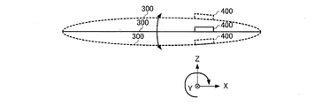
ところで、物理量検出装置400はプリント基板等に実装されるが、実装基板の設置環境によっては、例えば、実装基板が主面に垂直な方向に振動する場合がある。図6は、実装基板が振動する様子を模式的に示す図である。図6に示すように、実装基板300が振動すると、物理量検出装置400は周期的に回転方向が変わる微小な回転振動をすることになり、振動素子100に、検出軸(Y軸)の方向の角速度が加わる場合がある。   By the way, the physical quantity detection device 400 is mounted on a printed circuit board or the like. Depending on the installation environment of the mounting board, for example, the mounting board may vibrate in a direction perpendicular to the main surface. FIG. 6 is a diagram schematically showing how the mounting board vibrates. As shown in FIG. 6, when the mounting substrate 300 vibrates, the physical quantity detection device 400 performs minute rotational vibration that periodically changes the rotation direction, and causes the vibration element 100 to move in the direction of the detection axis (Y axis). Angular velocity may be added.

実装基板300が振動素子100の検出軸(Y軸)を中心として周波数f、最大振幅Ωで回転振動した場合、振動素子100に加わる角速度Ωは時間変数tを用いて次式(4)で表される。 When the mounting substrate 300 rotates and vibrates at the frequency f 1 and the maximum amplitude Ω 1 around the detection axis (Y axis) of the vibration element 100, the angular velocity Ω applied to the vibration element 100 is expressed by the following equation (4) using the time variable t. It is represented by

Figure 2015184157
Figure 2015184157

式(4)を式(3)に代入すると、駆動振動腕220,222が受けるコリオリ力は、次式(5)で表される。   When Expression (4) is substituted into Expression (3), the Coriolis force received by the drive vibrating arms 220 and 222 is expressed by the following Expression (5).

Figure 2015184157
Figure 2015184157

従って、式(5)より、2つの駆動周波数fdr+fおよびfdr−fで検出振動腕230,232の振動が励起(加振)され、第1検出信号および第2検出信号には、fdr+fとfdr−fの2つの周波数成分が含まれる。 Therefore, from the equation (5), the vibrations of the detection vibrating arms 230 and 232 are excited (vibrated) at two drive frequencies f dr + f 1 and f dr −f 1 , and the first detection signal and the second detection signal are , F dr + f 1 and f dr −f 1 are included.

ここで、図5から明らかなように、実装基板300の振動周波数fが離調周波数Δfに近く、fdr<fdtの場合(図5(A)参照)にfdr−fによるコリオリ力は、検出振動腕230,232の共振周波数fdtから遠い周波数であるため、fdr−fの周波数による検出振動は十分無視できるほどに微量である。同様に、fdr>fdtの場合(図5(B)参照)にfdr+fによるコリオリ力も、検出振動腕230,232の共振周波数fdtから遠い周波数であるため、fdr+fの周波数による検出振動は十分無視できるほどに微量である。 Here, as is apparent from FIG. 5, when the vibration frequency f 1 of the mounting board 300 is close to the detuning frequency Δf and f dr <f dt (see FIG. 5A) (see FIG. 5A), Coriolis due to f dr −f 1 . Since the force is a frequency far from the resonance frequency f dt of the detection vibrating arms 230 and 232, the detection vibration due to the frequency of f dr −f 1 is so small that it can be sufficiently ignored. Similarly, in the case of f dr > f dt (see FIG. 5B), the Coriolis force due to f dr + f 1 is also a frequency far from the resonance frequency f dt of the detection vibrating arms 230 and 232, and therefore f dr + f 1 The detected vibration due to frequency is so small that it can be ignored.

一方、実装基板300の振動周波数fが離調周波数Δfに近いと、fdr<fdtの場合(図5(A)参照)はfdr+fがfdtに近くなり、fdr>fdtの場合(図5(B)参照)はfdr−fがfdtに近くなるため、検出振動腕230,232が共振周波数fdtに近い周波数で大きく振動することになる。そうすると、検出電極40,42に発生する電荷量が大きくなりすぎて、差動増幅回路453の出力信号やAC増幅回路455の出力信号が飽和するおそれがある。また、AC増幅回路455の出力信号で飽和せずとも、これらの信号が同期検波回路456に入力され同期検波されると、検出回路450の出力信号が飽和するおそれがある。 On the other hand, when the vibration frequency f 1 of the mounting substrate 300 is close to the detuning frequency Δf, in the case of f dr <f dt (see FIG. 5A), f dr + f 1 is close to f dt , and f dr > f In the case of dt (see FIG. 5B), since f dr −f 1 is close to f dt , the detection vibrating arms 230 and 232 vibrate greatly at a frequency close to the resonance frequency f dt . Then, the amount of charge generated at the detection electrodes 40 and 42 becomes too large, and the output signal of the differential amplifier circuit 453 and the output signal of the AC amplifier circuit 455 may be saturated. Even if the output signals of the AC amplifier circuit 455 are not saturated, if these signals are input to the synchronous detection circuit 456 and synchronously detected, the output signal of the detection circuit 450 may be saturated.

例えば、振動素子100に、離調周波数Δf付近の周波数成分をもつ100dpsの回転振動が加わった場合、検出振動腕230,232の共振によって500倍されるとすると、50000dpsの検出信号が出力されてしまう。検出回路450の出力信号のダイナミックレンジが±300dpsを想定して設計されている場合、50000dpsの検出信号が入力されると検出回路450の出力信号が飽和する。   For example, when 100 dps rotational vibration having a frequency component near the detuning frequency Δf is applied to the vibration element 100, a detection signal of 50000 dps is output if the vibration is multiplied by 500 by the resonance of the detection vibrating arms 230 and 232. End up. When the dynamic range of the output signal of the detection circuit 450 is designed assuming ± 300 dps, the output signal of the detection circuit 450 is saturated when a detection signal of 50000 dps is input.

検出回路450の出力信号が最大出力電圧で飽和すると中心電圧(0点電圧)が低い方に変動し、検出回路450の出力信号が最小出力電圧で飽和すると中心電圧(0点電圧)が高い方に変動するので、いずれの場合も検出精度の低下や誤検出につながる。   When the output signal of the detection circuit 450 is saturated at the maximum output voltage, the center voltage (zero point voltage) fluctuates to the lower side, and when the output signal of the detection circuit 450 is saturated at the minimum output voltage, the center voltage (zero point voltage) is higher. Therefore, in either case, the detection accuracy is reduced and erroneous detection is caused.

特に、本実施形態に係る物理量検出装置400では、振動素子100の主面2a,2bに平行なY軸が検出軸であるため、主面2a,2bが実装基板300と平行となるように実装されると、検出軸が実装基板300の振動方向と一致しやすくなり、検出回路450の出力信号が飽和するおそれがある。   In particular, in the physical quantity detection device 400 according to the present embodiment, since the Y axis parallel to the main surfaces 2a and 2b of the vibration element 100 is the detection axis, the main surfaces 2a and 2b are mounted so as to be parallel to the mounting substrate 300. Then, the detection axis tends to coincide with the vibration direction of the mounting substrate 300, and the output signal of the detection circuit 450 may be saturated.

そこで、本実施形態では、AC増幅回路455の前段にフィルター回路454を設けており、フィルター回路454により、検出振動腕230,232の共振周波数fdtに近い周波数成分の信号を取り除く(正確には、大きく減衰させる)ようにしている。 Therefore, in the present embodiment, a filter circuit 454 is provided in front of the AC amplifier circuit 455, and a signal having a frequency component close to the resonance frequency f dt of the detection vibrating arms 230 and 232 is removed by the filter circuit 454 (more precisely, , Greatly attenuate).

具体的には、fdr<fdtとなるように振動素子100の構造を決めた場合は、フィルター回路454をローパスフィルターとして構成する。そして、フィルター回路454は、図7(A)に示すようなフィルター特性となるように、すなわち、fdrが通過帯域に含まれ、かつ、カットオフ周波数f<fdtとなるように構成される。このようにすれば、振動素子100の検出信号に含まれる周波数成分fdr+fの信号はフィルター回路454により取り除かれ、同期検波回路456では、fdr−fの周波数成分の信号のみが周波数fdrの信号で同期検波されるので、同期検波回路456の出力信号Sは次式(6)で表される。なお、式(6)においてαは定数である。 Specifically, when the structure of the vibration element 100 is determined so that f dr <f dt , the filter circuit 454 is configured as a low-pass filter. The filter circuit 454 is configured so as to have a filter characteristic as shown in FIG. 7A, that is, f dr is included in the passband and the cutoff frequency f c <f dt is satisfied. The In this way, the signal of the frequency component f dr + f 1 included in the detection signal of the vibration element 100 is removed by the filter circuit 454, and in the synchronous detection circuit 456, only the signal of the frequency component of f dr −f 1 is the frequency. Since synchronous detection is performed with the signal f dr , the output signal S of the synchronous detection circuit 456 is expressed by the following equation (6). In Expression (6), α is a constant.

Figure 2015184157
Figure 2015184157

式(6)の右辺第1項の周波数2fdr−fの信号は、平滑回路457で取り除かれるため、平滑回路457の出力信号には、右辺第2項の周波数fの信号のみ残る。 Since the signal having the frequency 2f dr -f 1 in the first term on the right side of Expression (6) is removed by the smoothing circuit 457, only the signal having the frequency f 1 in the second term on the right side remains in the output signal of the smoothing circuit 457.

一方、fdr>fdtとなるように振動素子100の構造を決めた場合は、フィルター回路454をハイパスフィルターとして構成する。そして、フィルター回路454は、図7(B)に示すようなフィルター特性となるように、すなわち、fdrが通過帯域に含まれ、かつ、カットオフ周波数f>fdtとなるように構成される。このようにすれば、振動素子100の検出信号に含まれる周波数成分fdr−fの信号はフィルター回路454により取り除かれ、同期検波回路456では、fdr+fの周波数成分の信号のみが周波数fdrの信号で同期検波されるので、同期検波回路456の出力信号Sは次式(7)で表される。なお、式(7)においてαは定数である。 On the other hand, when the structure of the vibration element 100 is determined so that f dr > f dt , the filter circuit 454 is configured as a high-pass filter. The filter circuit 454 is configured to have a filter characteristic as shown in FIG. 7B, that is, f dr is included in the passband and the cutoff frequency f c > f dt is satisfied. The In this way, the signal of the frequency component f dr −f 1 included in the detection signal of the vibration element 100 is removed by the filter circuit 454, and in the synchronous detection circuit 456, only the signal of the frequency component of f dr + f 1 is the frequency. Since synchronous detection is performed using the signal f dr , the output signal S of the synchronous detection circuit 456 is expressed by the following equation (7). In Expression (7), α is a constant.

Figure 2015184157
Figure 2015184157

式(7)の右辺第1項の周波数2fdr+fの信号は、平滑回路457で取り除かれるため、平滑回路457の出力信号には、右辺第2項の周波数fの信号のみ残る。 Since the signal of the frequency 2f dr + f 1 of the first term on the right side of Expression (7) is removed by the smoothing circuit 457, only the signal of the frequency f 1 of the second term on the right side remains in the output signal of the smoothing circuit 457.

なお、フィルター回路454をローパスフィルターとして構成した場合もハイパスフィルターとして構成した場合も、フィルター回路459(ローパスフィルター)のカットオフ周波数fを離調周波数Δfよりも十分低く設定し、フィルター回路459により、平滑回路457の出力信号に残る周波数fの信号を取り除いてもよい。 Even when configured as a high-pass filter may have configured the filter circuit 454 as a low pass filter, set sufficiently lower than the cutoff frequency f c of the detuning frequency Δf of the filter circuit 459 (low pass filter), a filter circuit 459 The signal of the frequency f 1 remaining in the output signal of the smoothing circuit 457 may be removed.

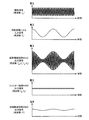
図8に、fdr<fdtであり、かつ、フィルター回路454がローパスフィルターとして構成されている場合に、振動素子100に周波数fの回転振動が加わった時に観測される信号波形の一例を示す。図8に示すように、差動増幅回路453の出力信号は、周波数fdrの駆動信号が回転振動による周波数fの信号で振幅変調された比較的大きな信号となるが、フィルター回路454の出力信号は周波数がfdr−fの小さな信号となるため、同期検波回路456の出力信号は周波数がfの小さな信号となり、検出回路450の出力信号が飽和しない。 FIG. 8 shows an example of a signal waveform observed when rotational vibration of the frequency f 1 is applied to the vibration element 100 when f dr <f dt and the filter circuit 454 is configured as a low-pass filter. Show. As shown in FIG. 8, the output signal of the differential amplifier circuit 453 is a relatively large signal in which the drive signal of the frequency f dr is amplitude-modulated by the signal of the frequency f 1 due to the rotational vibration, but the output of the filter circuit 454 Since the signal is a small signal having a frequency of f dr −f 1 , the output signal of the synchronous detection circuit 456 is a signal having a small frequency of f 1 , and the output signal of the detection circuit 450 is not saturated.

以上に説明したように、第1実施形態に係る物理量検出装置400によれば、フィルター回路454を設けたことにより、振動素子100の離調周波数Δfに近い周波数の回転振動や衝撃が加わっても、検出回路450の出力信号が飽和するおそれを低減することができる。従って、検出回路450の出力信号における中心電圧(0点電圧)の変動が抑制されるため、検出精度が高く、かつ、振動や衝撃にロバストで実装位置の自由度が高い堅牢な物理量検出装置400を実現することができる。   As described above, according to the physical quantity detection device 400 according to the first embodiment, by providing the filter circuit 454, even if rotational vibration or an impact with a frequency close to the detuning frequency Δf of the vibration element 100 is applied. The possibility that the output signal of the detection circuit 450 is saturated can be reduced. Therefore, since the fluctuation of the center voltage (zero point voltage) in the output signal of the detection circuit 450 is suppressed, the robust physical quantity detection device 400 has high detection accuracy, is robust against vibration and shock, and has a high degree of freedom in mounting position. Can be realized.

特に、フィルター回路454をAC増幅回路455の前段に設けたことにより、AC増幅回路455の出力信号が飽和するおそれや同期検波回路456の出力信号が飽和するおそれを低減することができるので、平滑回路457で回転振動による周波数fの信号を取り除く場合と比較しても有利である。 In particular, since the filter circuit 454 is provided before the AC amplifier circuit 455, the possibility that the output signal of the AC amplifier circuit 455 is saturated or the output signal of the synchronous detection circuit 456 is reduced can be reduced. This is also advantageous compared to the case where the circuit 457 removes the signal having the frequency f 1 due to the rotational vibration.

1−2.第2実施形態
第2実施形態に係る物理量検出装置400は、振動素子100の構造が第1実施形態と異なる。なお、第2実施形態に係る物理量検出装置の機能ブロック図は、図1と同様であるため、その図示及び説明を省略する。
1-2. Second Embodiment A physical quantity detection device 400 according to a second embodiment is different from the first embodiment in the structure of the vibration element 100. The functional block diagram of the physical quantity detection device according to the second embodiment is the same as that in FIG.

[振動素子の構成]
次に、第2実施形態に係る振動素子100について、図面を参照しながら説明する。図9および図10は、第2実施形態に係る振動素子100を模式的に示す平面図である。
[Configuration of vibrating element]
Next, the resonator element 100 according to the second embodiment will be described with reference to the drawings. 9 and 10 are plan views schematically showing the vibration element 100 according to the second embodiment.

なお、図9は、振動素子100を第1主面2a側から見た図であって、第1主面2a側の構成を説明するための図である。図10は、振動素子100を第1主面2a側から見た透視図であって、第2主面2b側の構成を説明するための図である。   FIG. 9 is a diagram of the vibration element 100 as viewed from the first main surface 2a side, and is a diagram for explaining the configuration on the first main surface 2a side. FIG. 10 is a perspective view of the vibration element 100 as viewed from the first main surface 2a side, and is a view for explaining the configuration on the second main surface 2b side.

以下、第2実施形態に係る振動素子100において、上述した第1実施形態に係る振動素子100の構成部材と同様の機能を有する部材については同一の符号を付し、その詳細な説明を省略する。   Hereinafter, in the vibration element 100 according to the second embodiment, members having the same functions as the constituent members of the vibration element 100 according to the first embodiment described above are denoted by the same reference numerals, and detailed description thereof is omitted. .

上述した第1実施形態に係る振動素子100では、図2に示すように、振動片1は、H型の振動片であった。これに対し、第2実施形態に係る振動素子100では、図9および図10に示すように、振動片1は、いわゆるダブルT型の振動片である。   In the resonator element 100 according to the first embodiment described above, as illustrated in FIG. 2, the resonator element 1 is an H-shaped resonator element. In contrast, in the resonator element 100 according to the second embodiment, as illustrated in FIGS. 9 and 10, the resonator element 1 is a so-called double T-type resonator element.

振動片1は、図9および図10に示すように、基部10と、連結腕210,212と、駆動振動腕220,222,224,226と、検出振動腕230,232と、支持部240,242と、梁部250,252,254,256と、駆動入力電極30と、駆動出力電極32と、第1検出電極40と、第2検出電極42と、第3検出電極44と、第4検出電極46と、駆動入力配線50と、駆動出力配線52と、第1検出配線60と、第2検出配線62と、第3検出配線64と、第4検出配線66と、を有している。   As shown in FIGS. 9 and 10, the resonator element 1 includes a base 10, connecting arms 210 and 212, driving vibrating arms 220, 222, 224 and 226, detection vibrating arms 230 and 232, a support portion 240, 242, beams 250, 252, 254, and 256, drive input electrode 30, drive output electrode 32, first detection electrode 40, second detection electrode 42, third detection electrode 44, and fourth detection. The electrode 46, the drive input wiring 50, the drive output wiring 52, the first detection wiring 60, the second detection wiring 62, the third detection wiring 64, and the fourth detection wiring 66 are included.

基部10、連結腕210,212、駆動振動腕220,222,224,226、検出振動腕230,232、支持部240,242および梁部250,252,254,256は、振動片1を構成している。   The base portion 10, the connecting arms 210 and 212, the driving vibration arms 220, 222, 224 and 226, the detection vibration arms 230 and 232, the support portions 240 and 242, and the beam portions 250, 252, 254 and 256 constitute the vibration piece 1. ing.

基部10は、中心点Gを有している。中心点Gの位置は、振動片1の重心の位置である。基部10の平面形状は、例えば矩形(略矩形)である。   The base 10 has a center point G. The position of the center point G is the position of the center of gravity of the resonator element 1. The planar shape of the base 10 is, for example, a rectangle (substantially rectangular).

第1連結腕210および第2連結腕212は、基部10から、X軸に沿って互いに反対方向に延出している。図示の例では、第1連結腕210は、基部10から−X軸方向に延出し、第2連結腕212は、基部10から+X軸方向に延出している。   The first connecting arm 210 and the second connecting arm 212 extend from the base 10 in opposite directions along the X axis. In the illustrated example, the first connecting arm 210 extends from the base 10 in the −X-axis direction, and the second connecting arm 212 extends from the base 10 in the + X-axis direction.

第1駆動振動腕220および第2駆動振動腕222は、第1連結腕210から、Y軸に沿って互いに反対方向に延出している。図示の例では、第1駆動振動腕220は、第1連結腕210から+Y軸方向に延出し、第2駆動振動腕222は、第1連結腕210から−Y軸方向に延出している。駆動振動腕220,222は、第1連結腕210を介して、基部10に接続されている。   The first drive vibrating arm 220 and the second drive vibrating arm 222 extend from the first connecting arm 210 in opposite directions along the Y axis. In the illustrated example, the first drive vibrating arm 220 extends from the first connecting arm 210 in the + Y-axis direction, and the second drive vibrating arm 222 extends from the first connecting arm 210 in the −Y-axis direction. The drive vibrating arms 220 and 222 are connected to the base 10 via the first connecting arm 210.

第3駆動振動腕224および第4駆動振動腕226は、第2連結腕212から、Y軸に沿って互いに反対方向に延出している。図示の例では、第3駆動振動腕224は、第2連結腕212から+Y軸方向に延出し、第4駆動振動腕226は、第2連結腕212から−Y軸方向に延出している。駆動振動腕224,226は、第2連結腕212を介して、基部10に接続されている。   The third drive vibrating arm 224 and the fourth drive vibrating arm 226 extend from the second connecting arm 212 in opposite directions along the Y axis. In the illustrated example, the third drive vibrating arm 224 extends from the second connection arm 212 in the + Y-axis direction, and the fourth drive vibration arm 226 extends from the second connection arm 212 in the −Y-axis direction. The drive vibrating arms 224 and 226 are connected to the base 10 via the second connecting arm 212.

第1検出振動腕230および第2検出振動腕232は、基部10から、Y軸に沿って互いに反対方向に延出している。図示の例では、第1検出振動腕230は、基部10から+Y軸方向に延出し、第2検出振動腕232は、基部10から−Y軸方向に延出している。検出振動腕230,232は、基部10に接続されている。   The first detection vibrating arm 230 and the second detection vibrating arm 232 extend from the base 10 in opposite directions along the Y axis. In the illustrated example, the first detection vibrating arm 230 extends from the base 10 in the + Y-axis direction, and the second detection vibrating arm 232 extends from the base 10 in the −Y-axis direction. The detection vibrating arms 230 and 232 are connected to the base 10.

振動腕220,222,224,226,230,232の先端には、幅広部5が設けられている。幅広部5は、振動腕220,222,224,226,230,232の他の部分より、幅(X軸方向の大きさ)が大きい。図示はしないが、幅広部5には、錘部が設けられていてもよい。該錘部の質量を調整することによって、振動腕220,222,224,226,230,232の振動の周波数を調整することができる。   A wide portion 5 is provided at the tip of the vibrating arms 220, 222, 224, 226, 230, and 232. The wide portion 5 has a larger width (size in the X-axis direction) than other portions of the vibrating arms 220, 222, 224, 226, 230, and 232. Although not shown, the wide portion 5 may be provided with a weight portion. By adjusting the mass of the weight portion, the vibration frequency of the vibrating arms 220, 222, 224, 226, 230, and 232 can be adjusted.

第1支持部240は、振動腕220,224,230よりも+Y軸方向側に設けられている。第2支持部242は、振動腕222,226,232よりも−Y軸方向側に設けられている。支持部240,242は、振動素子100が実装される際に、パッケージに固定される部分である。支持部240,242は、梁部250,252,254,256を介して、基部10を支持している。   The first support portion 240 is provided on the + Y axis direction side with respect to the vibrating arms 220, 224 and 230. The second support portion 242 is provided on the −Y axis direction side with respect to the vibrating arms 222, 226, and 232. The support portions 240 and 242 are portions that are fixed to the package when the vibration element 100 is mounted. The support portions 240 and 242 support the base portion 10 via the beam portions 250, 252, 254, and 256.

第1梁部250および第2梁部252は、基部10と第1支持部240とを連結している。図示の例では、第1梁部250は、基部10から、第1駆動振動腕220と第1検出振動腕230との間を通って、第1支持部240まで延出している。第2梁部252は、基部10から、第3駆動振動腕224と第1検出振動腕230との間を通って、第1支持部240まで延出している。   The first beam portion 250 and the second beam portion 252 connect the base portion 10 and the first support portion 240. In the illustrated example, the first beam portion 250 extends from the base portion 10 to the first support portion 240 through between the first drive vibrating arm 220 and the first detection vibrating arm 230. The second beam portion 252 extends from the base portion 10 to the first support portion 240 through between the third drive vibration arm 224 and the first detection vibration arm 230.

第3梁部254および第4梁部256は、基部10と第2支持部242とを連結している。図示の例では、第3梁部254は、基部10から、第2駆動振動腕222と第2検出振動腕232との間を通って、第2支持部242まで延出している。第4梁部256は、基部10から、第4駆動振動腕226と第2検出振動腕232との間を通って、第2支持部242まで延出している。   The third beam portion 254 and the fourth beam portion 256 connect the base portion 10 and the second support portion 242. In the illustrated example, the third beam portion 254 extends from the base portion 10 to the second support portion 242 through between the second drive vibrating arm 222 and the second detection vibrating arm 232. The fourth beam portion 256 extends from the base portion 10 to the second support portion 242 through between the fourth drive vibrating arm 226 and the second detection vibrating arm 232.

梁部250,252,254,256は、平面視において、略S字状の部分を有している。そのため、梁部250,252,254,256は、高い弾性を有することができる。これにより、支持部240,242は、振動腕220,222,224,226,230,232の振動を阻害することなく、梁部250,252,254,256を介して、基部10を支持することができる。   The beam portions 250, 252, 254, and 256 have a substantially S-shaped portion in plan view. Therefore, the beam portions 250, 252, 254, and 256 can have high elasticity. Thus, the support portions 240 and 242 support the base portion 10 through the beam portions 250, 252, 254, and 256 without hindering the vibration of the vibrating arms 220, 222, 224, 226, 230, and 232. Can do.

駆動入力電極30は、駆動振動腕220,222,224,226に設けられている。図示の例では、駆動入力電極30は、第1駆動振動腕220の側面3および幅広部5と、第2駆動振動腕222の側面3および幅広部5と、第3駆動振動腕224の主面(幅広部5以外の主面)2a,2bと、第4駆動振動腕226の主面(幅広部5以外の主面)2a,2bと、に設けられている。駆動入力電極30は、例えば、中心点Gを通りXZ平面に平行な面に関して、面対称に配置されている。駆動入力電極30は、駆動振動腕220,222,224,226を駆動させる信号(駆動信号)が入力される電極である。   The drive input electrode 30 is provided on the drive vibrating arms 220, 222, 224, and 226. In the illustrated example, the drive input electrode 30 includes the side surface 3 and the wide portion 5 of the first drive vibration arm 220, the side surface 3 and the wide portion 5 of the second drive vibration arm 222, and the main surface of the third drive vibration arm 224. (Main surfaces other than the wide portion 5) 2a, 2b and main surfaces (main surfaces other than the wide portion 5) 2a, 2b of the fourth drive vibrating arm 226 are provided. For example, the drive input electrode 30 is arranged in plane symmetry with respect to a plane passing through the center point G and parallel to the XZ plane. The drive input electrode 30 is an electrode to which a signal (drive signal) for driving the drive vibrating arms 220, 222, 224, and 226 is input.

駆動出力電極32は、駆動振動腕220,222,224,226に設けられている。図示の例では、駆動出力電極32は、第1駆動振動腕220の主面(幅広部5以外の部分の主面)2a,2bと、第2駆動振動腕222の主面(幅広部5以外の部分の主面)2a,2bと、第3駆動振動腕224の側面3および幅広部5と、第4駆動振動腕226の側面3および幅広部5と、に設けられている。駆動出力電極32は、例えば、中心点Gを通りXZ平面に平行な面に関して、面対称に配置されている。駆動出力電極32は、駆動振動腕220,222,224,226の屈曲に基づく信号を出力するための電極である。   The drive output electrode 32 is provided on the drive vibrating arms 220, 222, 224, and 226. In the illustrated example, the drive output electrode 32 includes main surfaces (main surfaces other than the wide portion 5) 2a and 2b of the first drive vibrating arm 220 and main surfaces (other than the wide portion 5) of the second drive vibrating arm 222. Of the third drive vibration arm 224, the side surface 3 and the wide portion 5 of the third drive vibration arm 224, and the side surface 3 and the wide portion 5 of the fourth drive vibration arm 226. For example, the drive output electrode 32 is arranged symmetrically with respect to a plane passing through the center point G and parallel to the XZ plane. The drive output electrode 32 is an electrode for outputting a signal based on the bending of the drive vibrating arms 220, 222, 224, and 226.

なお、図示はしないが、駆動入力電極30が設けられている位置に駆動出力電極32が設けられていてもよく、駆動出力電極32が設けられている位置に駆動入力電極30が設けられていてもよい。   Although not shown, the drive output electrode 32 may be provided at a position where the drive input electrode 30 is provided, and the drive input electrode 30 is provided at a position where the drive output electrode 32 is provided. Also good.

第1検出電極40は、第1検出振動腕230に設けられている。図示の例では、第1検出電極40は、第1検出振動腕230の主面(幅広部5以外の主面)2a,2bに設けられている。第1検出電極40は、コリオリ力による第1検出振動腕230の屈曲に基づく信号(第1検出信号)を検出するための電極である。   The first detection electrode 40 is provided on the first detection vibrating arm 230. In the illustrated example, the first detection electrode 40 is provided on the main surfaces (main surfaces other than the wide portion 5) 2a and 2b of the first detection vibrating arm 230. The first detection electrode 40 is an electrode for detecting a signal (first detection signal) based on the bending of the first detection vibrating arm 230 due to the Coriolis force.

第2検出電極42は、第1検出振動腕230に設けられている。図示の例では、第2検出電極42は、第1検出振動腕230の側面3および幅広部5に設けられている。第2検出電極42は、コリオリ力による第1検出振動腕230の屈曲に基づく信号(第1検出信号)を検出するための電極である。第2検出電極42は、例えば、第1検出信号に対して、基準となる電位を有する電極である。   The second detection electrode 42 is provided on the first detection vibrating arm 230. In the illustrated example, the second detection electrode 42 is provided on the side surface 3 and the wide portion 5 of the first detection vibrating arm 230. The second detection electrode 42 is an electrode for detecting a signal (first detection signal) based on the bending of the first detection vibrating arm 230 due to the Coriolis force. For example, the second detection electrode 42 is an electrode having a reference potential with respect to the first detection signal.

第3検出電極44は、第2検出振動腕232に設けられている。図示の例では、第3検出電極44は、第2検出振動腕232の主面(幅広部5以外の主面)2a,2bに設けられている。第3検出電極44は、例えば、第1検出電極40と、中心点Gを通りXZ平面に平行な面に関して、面対称に配置されている。第3検出電極44は、コリオリ力による第2検出振動腕232の屈曲に基づく信号(第2検出信号)を検出するための電極である。   The third detection electrode 44 is provided on the second detection vibrating arm 232. In the illustrated example, the third detection electrode 44 is provided on the main surfaces (main surfaces other than the wide portion 5) 2 a and 2 b of the second detection vibrating arm 232. For example, the third detection electrode 44 is arranged symmetrically with respect to the first detection electrode 40 and a plane that passes through the center point G and is parallel to the XZ plane. The third detection electrode 44 is an electrode for detecting a signal (second detection signal) based on the bending of the second detection vibrating arm 232 due to the Coriolis force.

第4検出電極46は、第2検出振動腕232に設けられている。図示の例では、第4検出電極46は、第2検出振動腕232の側面3および幅広部5に設けられている。第4検出電極46は、例えば、第2検出電極42と、中心点Gを通りXZ平面に平行な面に関して、面対称に配置されている。第4検出電極46は、コリオリ力による第2検出振動腕232の屈曲に基づく信号(第2検出信号)を検出するための電極である。第4検出電極46は、例えば、第2検出信号に対して、基準となる電位を有する電極である。   The fourth detection electrode 46 is provided on the second detection vibrating arm 232. In the illustrated example, the fourth detection electrode 46 is provided on the side surface 3 and the wide portion 5 of the second detection vibrating arm 232. For example, the fourth detection electrode 46 is arranged in plane symmetry with respect to the second detection electrode 42 and a plane passing through the center point G and parallel to the XZ plane. The fourth detection electrode 46 is an electrode for detecting a signal (second detection signal) based on the bending of the second detection vibrating arm 232 due to the Coriolis force. For example, the fourth detection electrode 46 is an electrode having a reference potential with respect to the second detection signal.

なお、図示はしないが、振動腕220,222,224,226,230,232の主面2a,2bには、溝部が設けられていてもよく、電極30,32,40,44は、該溝部内に設けられていてもよい。   Although not shown, grooves may be provided on the main surfaces 2a and 2b of the vibrating arms 220, 222, 224, 226, 230, and 232, and the electrodes 30, 32, 40, and 44 It may be provided inside.

駆動入力配線50は、基部10と、連結腕210,212と、第2支持部242と、第3梁部254と、に設けられている。図示の例では、駆動入力配線50は、基部10の第1主面2aおよび側面3と、第1連結腕210の第1主面2aと、第2連結腕212の主面2a,2bおよび側面3と、第2支持部242の主面2a,2bおよび側面3と、第3梁部254の側面3と、に設けられている。駆動入力配線50によって、振動腕220,222,224,226に設けられた駆動入力電極30は、互いに電気的に接続されている。第2支持部242に設けられた駆動入力配線50は、端子部50aである。図示の例では、端子部50aの平面形状は、矩形である。端子部50aは、外部部材(例えば、ボンディングワイヤー)に接続され、駆動回路440から出力される駆動信号は、外部部材および駆動入力配線50を介して駆動入力電極30に入力される。   The drive input wiring 50 is provided on the base 10, the connecting arms 210 and 212, the second support portion 242, and the third beam portion 254. In the illustrated example, the drive input wiring 50 includes the first main surface 2 a and the side surface 3 of the base 10, the first main surface 2 a of the first connecting arm 210, and the main surfaces 2 a and 2 b and the side surfaces of the second connecting arm 212. 3, the main surfaces 2 a and 2 b and the side surface 3 of the second support portion 242, and the side surface 3 of the third beam portion 254. The drive input electrodes 30 provided on the vibrating arms 220, 222, 224, and 226 are electrically connected to each other by the drive input wiring 50. The drive input wiring 50 provided in the second support part 242 is a terminal part 50a. In the illustrated example, the planar shape of the terminal portion 50a is a rectangle. The terminal portion 50 a is connected to an external member (for example, a bonding wire), and a drive signal output from the drive circuit 440 is input to the drive input electrode 30 via the external member and the drive input wiring 50.

駆動出力配線52は、基部10と、連結腕210,212と、第1支持部240と、第1梁部250と、に設けられている。図示の例では、駆動出力配線52は、基部10の第2主面2bと、第1連結腕210の主面2a,2bおよび側面3と、第2連結腕212の第2主面2bおよび側面3と、第1支持部240の主面2a,2bおよび側面3と、第1梁部250の第2主面2bおよび側面3と、に設けられている。駆動出力配線52によって、振動腕220,222,224,226に設けられた駆動出力電極32は、互いに電気的に接続されている。第1支持部240に設けられた駆動出力配線52は、端子部52aである。図示の例では、端子部52aの平面形状は、矩形である。端子部52aは、外部部材(例えば、ボンディングワイヤー)に接続され、駆動出力電極32から出力される信号は、駆動出力配線52および外部部材を介して駆動回路440に入力される。   The drive output wiring 52 is provided on the base 10, the connecting arms 210 and 212, the first support portion 240, and the first beam portion 250. In the illustrated example, the drive output wiring 52 includes the second main surface 2b of the base 10, the main surfaces 2a and 2b and the side surface 3 of the first connecting arm 210, and the second main surface 2b and the side surface of the second connecting arm 212. 3, the main surfaces 2 a and 2 b and the side surfaces 3 of the first support portion 240, and the second main surface 2 b and the side surfaces 3 of the first beam portion 250. The drive output electrodes 32 provided on the vibrating arms 220, 222, 224, and 226 are electrically connected to each other by the drive output wiring 52. The drive output wiring 52 provided in the first support part 240 is a terminal part 52a. In the illustrated example, the planar shape of the terminal portion 52a is a rectangle. The terminal portion 52a is connected to an external member (for example, a bonding wire), and a signal output from the drive output electrode 32 is input to the drive circuit 440 via the drive output wiring 52 and the external member.

第1検出配線60は、基部10と、第1支持部240と、第2梁部252と、に設けられている。図示の例では、第1検出配線60は、基部10の主面2a,2bと、第1支持部240の主面2a,2bおよび側面3と、第2梁部252の第1主面2aおよび側面3と、に設けられている。第1検出配線60は、第1検出電極40に接続されている。第1支持部240に設けられた第1検出配線60は、端子部60aである。図示の例では、端子部60aの平面形状は、矩形である。端子部60aは、外部部材(例えば、ボンディングワイヤー)に接続され、第1検出電極40から出力される第1検出信号は、第1検出配線60および外部部材を介して検出回路450のチャージアンプ451に入力される。   The first detection wiring 60 is provided on the base portion 10, the first support portion 240, and the second beam portion 252. In the illustrated example, the first detection wiring 60 includes the main surfaces 2a and 2b of the base portion 10, the main surfaces 2a and 2b and the side surface 3 of the first support portion 240, the first main surface 2a of the second beam portion 252, and It is provided on the side surface 3. The first detection wiring 60 is connected to the first detection electrode 40. The 1st detection wiring 60 provided in the 1st support part 240 is the terminal part 60a. In the illustrated example, the planar shape of the terminal portion 60a is a rectangle. The terminal portion 60a is connected to an external member (for example, a bonding wire), and the first detection signal output from the first detection electrode 40 is a charge amplifier 451 of the detection circuit 450 via the first detection wiring 60 and the external member. Is input.

第2検出配線62は、基部10と、第1支持部240と、第2梁部252と、に設けられている。図示の例では、第2検出配線62は、基部10の主面2a,2bおよび側面3と、第1支持部240の主面2a,2bおよび側面3と、第2梁部252の主面2a,2bおよび側面3と、に設けられている。第2検出配線62は、第2検出電極42に接続されている。第1支持部240に設けられた第2検出配線62は、端子部62aである。図示の例では、端子部62aの平面形状は、矩形である。端子部62aは、外部部材(例えば、ボンディングワイヤー)に接続され、第2検出電極42には、第2検出配線62および外部部材を介して固定された電位、具体的には、グランド電位が入力される。   The second detection wiring 62 is provided on the base portion 10, the first support portion 240, and the second beam portion 252. In the illustrated example, the second detection wiring 62 includes the main surfaces 2 a and 2 b and the side surface 3 of the base portion 10, the main surfaces 2 a and 2 b and the side surface 3 of the first support portion 240, and the main surface 2 a of the second beam portion 252. , 2b and the side surface 3 are provided. The second detection wiring 62 is connected to the second detection electrode 42. The second detection wiring 62 provided in the first support part 240 is a terminal part 62a. In the illustrated example, the planar shape of the terminal portion 62a is a rectangle. The terminal portion 62a is connected to an external member (for example, a bonding wire), and a potential fixed to the second detection electrode 42 via the second detection wiring 62 and the external member, specifically, a ground potential is input. Is done.

第3検出配線64は、基部10と、第2支持部242と、第4梁部256と、に設けられている。図示の例では、第3検出配線64は、基部10の主面2a,2bと、第2支持部242の主面2a,2bおよび側面3と、第4梁部256の第1主面2aおよび側面3と、に設けられている。第3検出配線64は、第3検出電極44に接続されている。第2支持部242に設けられた第3検出配線64は、端子部64aである。図示の例では、端子部64aの平面形状は、矩形である。端子部64aは、外部部材(例えば、ボンディングワイヤー)に接続され、第3検出電極44から出力される第2検出信号は、第3検出配線64および外部部材を介して検出回路450のチャージアンプ452に入力される。   The third detection wiring 64 is provided on the base portion 10, the second support portion 242, and the fourth beam portion 256. In the illustrated example, the third detection wiring 64 includes the main surfaces 2 a and 2 b of the base portion 10, the main surfaces 2 a and 2 b and the side surface 3 of the second support portion 242, and the first main surface 2 a and the fourth beam portion 256. It is provided on the side surface 3. The third detection wiring 64 is connected to the third detection electrode 44. The 3rd detection wiring 64 provided in the 2nd support part 242 is terminal part 64a. In the illustrated example, the planar shape of the terminal portion 64a is a rectangle. The terminal portion 64a is connected to an external member (for example, a bonding wire), and the second detection signal output from the third detection electrode 44 is a charge amplifier 452 of the detection circuit 450 via the third detection wiring 64 and the external member. Is input.

第4検出配線66は、基部10と、第2支持部242と、第4梁部256と、に設けられている。図示の例では、第4検出配線66は、基部10の主面2a,2bおよび側面3と、第2支持部242の主面2a,2bおよび側面3と、第4梁部256の主面2a,2bおよび側面3と、に設けられている。第4検出配線66は、第4検出電極46に接続されている。第2支持部242に設けられた第4検出配線66は、端子部66aである。図示の例では、端子部66aの平面形状は、矩形である。端子部66aは、外部部材(例えば、ボンディングワイヤー)に接続され、第4検出電極46には、第4検出配線66および外部部材を介して固定された電位、具体的には、グランド電位が入力される。   The fourth detection wiring 66 is provided on the base portion 10, the second support portion 242, and the fourth beam portion 256. In the illustrated example, the fourth detection wiring 66 includes the main surfaces 2 a and 2 b and the side surface 3 of the base portion 10, the main surfaces 2 a and 2 b and the side surface 3 of the second support portion 242, and the main surface 2 a of the fourth beam portion 256. , 2b and the side surface 3 are provided. The fourth detection wiring 66 is connected to the fourth detection electrode 46. The fourth detection wiring 66 provided in the second support part 242 is a terminal part 66a. In the illustrated example, the planar shape of the terminal portion 66a is a rectangle. The terminal portion 66a is connected to an external member (for example, a bonding wire), and a potential fixed to the fourth detection electrode 46 via the fourth detection wiring 66 and the external member, specifically, a ground potential is input. Is done.

なお、図9,10において、振動片1の側面3に設けられている電極30,32,40,42,44,46、配線50,52,60,62,64,66を、太線で示している。   9 and 10, the electrodes 30, 32, 40, 42, 44, 46 and the wirings 50, 52, 60, 62, 64, 66 provided on the side surface 3 of the resonator element 1 are indicated by bold lines. Yes.

次に、振動素子100の動作について説明する。図11(A)および図11(B)は、振動素子100の動作を説明するための平面図である。なお、便宜上、図11(A)および図11(B)では、基部10、連結腕210,212、および振動腕220,222,224,226,230,232以外の部材の図示を省略している。   Next, the operation of the vibration element 100 will be described. FIG. 11A and FIG. 11B are plan views for explaining the operation of the vibration element 100. For convenience, in FIG. 11A and FIG. 11B, illustration of members other than the base 10, the connecting arms 210 and 212, and the vibrating arms 220, 222, 224, 226, 230, and 232 is omitted. .

図11(A)に示すように、振動素子100は、角速度が加わらない状態において、駆動振動腕220,222,224,226に設けられた駆動入力電極30に所定の交流電圧が印加されると、XY平面内において矢印Aの方向に屈曲振動を行う(駆動モード)。このとき、駆動振動腕220,222と、駆動振動腕224,226とは、中心点Gを通りYZ平面に平行な面に関して、面対称の振動を行う。そのため、基部10、連結腕210,212、および検出振動腕230,232は、ほとんど振動しない。   As shown in FIG. 11A, when a predetermined AC voltage is applied to the drive input electrode 30 provided in the drive vibrating arms 220, 222, 224, and 226 in the vibration element 100 in a state where no angular velocity is applied. Then, bending vibration is performed in the direction of arrow A in the XY plane (drive mode). At this time, the drive vibrating arms 220 and 222 and the drive vibrating arms 224 and 226 perform plane-symmetric vibration with respect to a plane passing through the center point G and parallel to the YZ plane. Therefore, the base 10, the connecting arms 210 and 212, and the detection vibrating arms 230 and 232 hardly vibrate.

駆動振動腕220,222,224,226がこのような駆動振動を行っている状態で、図11(B)に示すように、振動素子100にZ軸まわりの角速度ωが加わると、駆動振動腕220,222,224,226にコリオリ力が働く。これにより、駆動振動腕220,222,224,226が矢印Bの方向に振動する。この矢印Bの方向の振動は、中心点Gに対して周方向の振動である。そして、駆動振動腕220,222,224,226の振動によって、連結腕210,212が矢印Bの方向に振動する。この振動が基部10を介して、検出振動腕230,232に伝達され、検出振動腕230,232を矢印Cで示すように振動させる(検出モード)。矢印Cの方向の振動は、中心点Gに対して矢印Bとは周方向に反対向きの振動である。この検出振動腕230,232の屈曲振動により、第1検出電極40および第3検出電極44には、それぞれ、第1検出信号および第2検出信号が発生する。   When the driving vibration arms 220, 222, 224, and 226 are performing such driving vibration, as shown in FIG. 11B, when the angular velocity ω around the Z axis is applied to the vibration element 100, the driving vibration arms Coriolis force acts on 220, 222, 224 and 226. As a result, the drive vibrating arms 220, 222, 224, and 226 vibrate in the direction of arrow B. The vibration in the direction of the arrow B is a vibration in the circumferential direction with respect to the center point G. Then, the connecting arms 210 and 212 vibrate in the direction of arrow B by the vibrations of the drive vibrating arms 220, 222, 224 and 226. This vibration is transmitted to the detection vibration arms 230 and 232 via the base 10, and vibrates the detection vibration arms 230 and 232 as indicated by an arrow C (detection mode). The vibration in the direction of the arrow C is a vibration in the direction opposite to the arrow B with respect to the center point G in the circumferential direction. Due to the bending vibration of the detection vibrating arms 230 and 232, a first detection signal and a second detection signal are generated at the first detection electrode 40 and the third detection electrode 44, respectively.

この時、第1検出信号の電気的極性と第2検出信号の電気的極性は逆である。例えば、第1検出電極40に正の電荷δ+が発生する時には第3検出電極44に負の電荷δ−が発生し、第1検出電極40に負の電荷δ−が発生する時には第3検出電極44に正の電荷δ+が発生する。第1検出信号は端子部60aから検出回路450に出力され、第2検出信号は端子部64aから検出回路450に出力され、検出回路450は、これらの検出信号によってZ軸まわりの角速度を求めることができる。   At this time, the electrical polarity of the first detection signal is opposite to the electrical polarity of the second detection signal. For example, when a positive charge δ + is generated at the first detection electrode 40, a negative charge δ− is generated at the third detection electrode 44, and when a negative charge δ− is generated at the first detection electrode 40, the third detection electrode. A positive charge δ + is generated at 44. The first detection signal is output from the terminal unit 60a to the detection circuit 450, the second detection signal is output from the terminal unit 64a to the detection circuit 450, and the detection circuit 450 obtains the angular velocity around the Z axis based on these detection signals. Can do.

本実施形態に係る物理量検出装置400では、振動素子100の主面2a,2bに垂直なZ軸が検出軸であるため、図6に示したように、主面2a,2bが実装基板300と平行となるように実装されても、検出軸が実装基板300の振動方向と一致せず、検出回路450の出力信号が飽和するおそれはほとんどない。しかしながら、図12に示すように、主面2a,2bが実装基板300と垂直となるように実装される場合もあり、この場合は、検出軸が実装基板300の振動方向と一致しやすくなり、検出回路450の出力信号が飽和するおそれがある。   In the physical quantity detection device 400 according to this embodiment, since the Z axis perpendicular to the main surfaces 2a and 2b of the vibration element 100 is the detection axis, the main surfaces 2a and 2b are connected to the mounting substrate 300 as shown in FIG. Even if they are mounted in parallel, the detection axis does not coincide with the vibration direction of the mounting substrate 300, and there is almost no possibility that the output signal of the detection circuit 450 is saturated. However, as shown in FIG. 12, the main surfaces 2a and 2b may be mounted so as to be perpendicular to the mounting substrate 300. In this case, the detection axis easily matches the vibration direction of the mounting substrate 300. The output signal of the detection circuit 450 may be saturated.

しかしながら、本実施形態に係る物理量検出装置400でも、AC増幅回路455の前段に第1実施形態と同様のフィルター回路454が設けられているため、実装基板300が離調周波数Δfに近い周波数で回転振動しても、フィルター回路454により、fdtに近い周波数成分の信号は取り除かれる。これにより、検出回路450の出力信号が飽和するおそれを低減させている。従って、検出回路450の出力信号における中心電圧(0点電圧)の変動が抑制されるため、検出精度が高く、かつ、振動や衝撃にロバストで実装位置の自由度が高い堅牢な物理量検出装置400を実現することができる。 However, in the physical quantity detection device 400 according to this embodiment, the filter circuit 454 similar to that of the first embodiment is provided in the previous stage of the AC amplifier circuit 455, so that the mounting substrate 300 rotates at a frequency close to the detuning frequency Δf. Even if it vibrates, the filter circuit 454 removes a signal having a frequency component close to f dt . Thereby, the possibility that the output signal of the detection circuit 450 is saturated is reduced. Therefore, since the fluctuation of the center voltage (zero point voltage) in the output signal of the detection circuit 450 is suppressed, the robust physical quantity detection device 400 has high detection accuracy, is robust against vibration and shock, and has a high degree of freedom in mounting position. Can be realized.

1−3.第3実施形態
図13は、第3実施形態に係る物理量検出装置400の機能ブロック図である。図13において図1と同じ構成要素には同じ符号を付している。図13に示すように、第3実施形態に係る物理量検出装置400では、差動増幅回路453の出力信号は、AC増幅回路455に入力され、AC増幅回路455でAC増幅された信号がフィルター回路454に入力される。
1-3. Third Embodiment FIG. 13 is a functional block diagram of a physical quantity detection device 400 according to a third embodiment. In FIG. 13, the same components as those in FIG. As shown in FIG. 13, in the physical quantity detection device 400 according to the third embodiment, the output signal of the differential amplifier circuit 453 is input to the AC amplifier circuit 455, and the signal amplified by the AC amplifier circuit 455 is filtered. 454 is input.

フィルター回路454は、第1実施形態と同様に、カットオフ周波数fが、振動素子100の駆動モードの共振周波数fdrと検出モードの共振周波数fdtとの間にあり、通過帯域に駆動モードの共振周波数fdrを含むフィルター部として機能する。フィルター回路454は、振動素子100がfdr<fdtの関係にある場合はローパスフィルターとして構成され、振動素子100がfdr>fdtの関係にある場合はハイパスフィルターとして構成される。フィルター回路454の出力信号は、同期検波回路456に入力される。 Similarly to the first embodiment, the filter circuit 454 has a cutoff frequency f c between the resonance frequency f dr of the drive mode of the vibration element 100 and the resonance frequency f dt of the detection mode, and the drive mode is in the pass band. It functions as a filter part including the resonance frequency f dr of. The filter circuit 454 is configured as a low-pass filter when the vibration element 100 has a relationship of f dr <f dt , and is configured as a high-pass filter when the vibration element 100 has a relationship of f dr > f dt . The output signal of the filter circuit 454 is input to the synchronous detection circuit 456.

第3実施形態に係る物理量検出装置400のその他の構成は、第1実施形態又は第2実施形態に係る物理量検出装置400と同じであるため、説明を省略する。   Since the other configuration of the physical quantity detection device 400 according to the third embodiment is the same as that of the physical quantity detection device 400 according to the first embodiment or the second embodiment, the description thereof is omitted.

この第3実施形態に係る物理量検出装置400によれば、第1実施形態又は第2実施形態に係る物理量検出装置400と同様に、AC増幅回路455の前段にフィルター回路454を設けたことにより、振動素子100の離調周波数Δfに近い周波数の回転振動が加わっても、検出回路450の出力信号が飽和するおそれを低減することができる。従って、検出回路450の出力信号における中心電圧(0点電圧)の変動が抑制されるため、検出精度が高く、かつ、振動や衝撃にロバストで実装位置の自由度が高い堅牢な物理量検出装置400を実現することができる。   According to the physical quantity detection device 400 according to the third embodiment, like the physical quantity detection device 400 according to the first embodiment or the second embodiment, the filter circuit 454 is provided in the previous stage of the AC amplification circuit 455. Even if rotational vibration having a frequency close to the detuning frequency Δf of the vibration element 100 is applied, the possibility that the output signal of the detection circuit 450 is saturated can be reduced. Therefore, since the fluctuation of the center voltage (zero point voltage) in the output signal of the detection circuit 450 is suppressed, the robust physical quantity detection device 400 has high detection accuracy, is robust against vibration and shock, and has a high degree of freedom in mounting position. Can be realized.

特に、フィルター回路454を同期検波回路456の前段に設けたことにより、同期検波回路456の出力信号が飽和するおそれを低減することができるので、平滑回路457で回転振動による周波数fの信号を取り除く場合と比較しても有利である。 In particular, by providing the filter circuit 454 in the preceding stage of the synchronous detection circuit 456, the possibility that the output signal of the synchronous detection circuit 456 is saturated can be reduced, so that the smoothing circuit 457 generates a signal having the frequency f 1 due to rotational vibration. It is advantageous compared with the case of removing.

1−4.第4実施形態
第4実施形態に係る物理量検出装置400は、フィルター回路454がバンドパスフィルターとして構成される点が、第1実施形態〜第3実施形態に係る物理量検出装置と異なる。第4実施形態に係る物理量検出装置の機能ブロック図は、図1又は図13と同様であるため、その図示及び説明を省略する。
1-4. Fourth Embodiment A physical quantity detection device 400 according to a fourth embodiment is different from the physical quantity detection device according to the first to third embodiments in that the filter circuit 454 is configured as a bandpass filter. Since the functional block diagram of the physical quantity detection device according to the fourth embodiment is the same as FIG. 1 or FIG. 13, its illustration and description are omitted.

図14は、本実施形態に係るフィルター回路454のフィルター特性の一例を示す図である。図14に示すように、フィルター回路454は、fdrが通過帯域に含まれ、かつ、低周波数側のカットオフ周波数fc1が駆動モードの共振周波数fdrと離調周波数Δfとの差fdr−Δfよりも大きく、かつ、高周波数側のカットオフ周波数fc2が駆動モードの共振周波数fdrと離調周波数Δfとの和fdr+Δfよりも小さくなるように構成される。このようにすれば、離調周波数Δfに近い周波数fの回転振動が加わった時に振動素子100の検出信号に含まれる周波数成分fdr−fの信号も周波数成分fdr+fの信号もフィルター回路454により取り除かれ、同期検波回路456ではこれらの信号が同期検波されない。 FIG. 14 is a diagram illustrating an example of the filter characteristics of the filter circuit 454 according to the present embodiment. As shown in FIG. 14, the filter circuit 454 includes f dr in the pass band, and the cut-off frequency f c1 on the low frequency side is the difference f dr between the resonance frequency f dr in the drive mode and the detuning frequency Δf. The cutoff frequency f c2 on the high frequency side is larger than −Δf and smaller than the sum f dr + Δf of the resonance frequency f dr and the detuning frequency Δf in the driving mode. In this way, when the rotational vibration of the frequency f 1 close to the detuning frequency Δf is applied, the signal of the frequency component f dr −f 1 and the signal of the frequency component f dr + f 1 included in the detection signal of the vibration element 100 are both. These signals are removed by the filter circuit 454, and these signals are not synchronously detected by the synchronous detection circuit 456.

従って、第4実施形態に係る物理量検出装置400によれば、第1実施形態〜第3実施形態に係る物理量検出装置400と比較して、同期検波回路456の出力信号が飽和するおそれをさらに低減することができる。   Therefore, according to the physical quantity detection device 400 according to the fourth embodiment, the possibility that the output signal of the synchronous detection circuit 456 is saturated is further reduced as compared with the physical quantity detection device 400 according to the first to third embodiments. can do.

2.電子機器
次に、本実施形態に係る電子機器について、図面を参照しながら説明する。本実施形態に係る電子機器は、本発明に係る物理量検出装置を含む。以下では、本発明に係る物理量検出装置として、物理量検出装置400を含む電子機器について、説明する。
2. Next, an electronic device according to the present embodiment will be described with reference to the drawings. The electronic apparatus according to the present embodiment includes the physical quantity detection device according to the present invention. Hereinafter, an electronic apparatus including the physical quantity detection device 400 will be described as the physical quantity detection device according to the present invention.

図15は、本実施形態に係る電子機器として、モバイル型(またはノート型)のパーソナルコンピューター1100を模式的に示す斜視図である。   FIG. 15 is a perspective view schematically showing a mobile (or notebook) personal computer 1100 as the electronic apparatus according to the present embodiment.

図15に示すように、パーソナルコンピューター1100は、キーボード1102を備えた本体部1104と、表示部1108を有する表示ユニット1106と、により構成され、表示ユニット1106は、本体部1104に対しヒンジ構造部を介して回動可能に支持されている。   As shown in FIG. 15, the personal computer 1100 includes a main body portion 1104 having a keyboard 1102 and a display unit 1106 having a display portion 1108, and the display unit 1106 has a hinge structure portion with respect to the main body portion 1104. It is supported so that rotation is possible.

このようなパーソナルコンピューター1100には、物理量検出装置400が内蔵されている。   Such a personal computer 1100 incorporates a physical quantity detection device 400.

図16は、本実施形態に係る電子機器として、携帯電話機(PHSも含む)1200を模式的に示す斜視図である。   FIG. 16 is a perspective view schematically showing a mobile phone (including PHS) 1200 as an electronic apparatus according to the present embodiment.

図16に示すように、携帯電話機1200は、複数の操作ボタン1202、受話口1204および送話口1206を備え、操作ボタン1202と受話口1204との間には、表示部1208が配置されている。   As shown in FIG. 16, the mobile phone 1200 includes a plurality of operation buttons 1202, an earpiece 1204, and a mouthpiece 1206, and a display unit 1208 is disposed between the operation buttons 1202 and the earpiece 1204. .

このような携帯電話機1200には、物理量検出装置400が内蔵されている。   Such a cellular phone 1200 incorporates a physical quantity detection device 400.

図17は、本実施形態に係る電子機器として、デジタルスチルカメラ1300を模式的に示す斜視図である。なお、図17には、外部機器との接続についても簡易的に示している。   FIG. 17 is a perspective view schematically showing a digital still camera 1300 as the electronic apparatus according to the present embodiment. Note that FIG. 17 simply shows connection with an external device.

ここで、通常のカメラは、被写体の光像により銀塩写真フィルムを感光するのに対し、デジタルスチルカメラ1300は、被写体の光像をCCD(Charge Coupled Device)などの撮像素子により光電変換して撮像信号(画像信号)を生成する。   Here, an ordinary camera sensitizes a silver halide photographic film with a light image of a subject, whereas a digital still camera 1300 photoelectrically converts a light image of a subject with an image sensor such as a CCD (Charge Coupled Device). An imaging signal (image signal) is generated.

デジタルスチルカメラ1300におけるケース(ボディー)1302の背面には、表示部1310が設けられ、CCDによる撮像信号に基づいて表示を行う構成になっており、表示部1310は、被写体を電子画像として表示するファインダーとして機能する。   A display unit 1310 is provided on the back of a case (body) 1302 in the digital still camera 1300, and is configured to display based on an imaging signal from the CCD. The display unit 1310 displays an object as an electronic image. Functions as a viewfinder.

また、ケース1302の正面側(図中裏面側)には、光学レンズ(撮像光学系)やCCDなどを含む受光ユニット1304が設けられている。   A light receiving unit 1304 including an optical lens (imaging optical system), a CCD, and the like is provided on the front side (the back side in the drawing) of the case 1302.

撮影者が表示部1310に表示された被写体像を確認し、シャッターボタン1306を押下すると、その時点におけるCCDの撮像信号が、メモリー1308に転送・格納される。   When the photographer confirms the subject image displayed on the display unit 1310 and presses the shutter button 1306, the CCD image pickup signal at that time is transferred and stored in the memory 1308.

また、このデジタルスチルカメラ1300においては、ケース1302の側面に、ビデオ信号出力端子1312と、データ通信用の入出力端子1314とが設けられている。そして、ビデオ信号出力端子1312には、テレビモニター1430が、データ通信用の入出力端子1314には、パーソナルコンピューター1440が、それぞれ必要に応じて接続される。さらに、所定の操作により、メモリー1308に格納された撮像信号が、テレビモニター1430や、パーソナルコンピューター1440に出力される構成になっている。   In the digital still camera 1300, a video signal output terminal 1312 and an input / output terminal 1314 for data communication are provided on the side surface of the case 1302. A television monitor 1430 is connected to the video signal output terminal 1312 and a personal computer 1440 is connected to the input / output terminal 1314 for data communication, if necessary. Further, the imaging signal stored in the memory 1308 is output to the television monitor 1430 or the personal computer 1440 by a predetermined operation.

このようなデジタルスチルカメラ1300には、物理量検出装置400が内蔵されている。   Such a digital still camera 1300 incorporates a physical quantity detection device 400.

なお、物理量検出装置400を備えた電子機器は、図15に示すパーソナルコンピューター(モバイル型パーソナルコンピューター)、図16に示す携帯電話機、図17に示すデジタルスチルカメラの他にも、例えば、インクジェット式吐出装置(例えばインクジェットプリンター)、ラップトップ型パーソナルコンピューター、テレビ、ビデオカメラ、ビデオテープレコーダー、各種ナビゲーション装置、ページャー、電子手帳(通信機能付も含む)、電子辞書、電卓、電子ゲーム機器、ヘッドマウントディスプレイ、ワードプロセッサー、ワークステーション、テレビ電話、防犯用テレビモニター、電子双眼鏡、POS端末、医療機器(例えば電子体温計、血圧計、血糖計、心電図計測装置、超音波診断装置、電子内視鏡)、魚群探知機、各種測定機器、計器類(例えば、車両、航空機、ロケット、船舶の計器類)、ロボットや人体などの姿勢制御、フライトシミュレーターなどに適用することができる。   In addition to the personal computer (mobile personal computer) shown in FIG. 15, the mobile phone shown in FIG. 16, and the digital still camera shown in FIG. Devices (for example, inkjet printers), laptop personal computers, televisions, video cameras, video tape recorders, various navigation devices, pagers, electronic notebooks (including those with communication functions), electronic dictionaries, calculators, electronic game machines, head-mounted displays , Word processor, workstation, video phone, security TV monitor, electronic binoculars, POS terminal, medical equipment (eg, electronic thermometer, blood pressure monitor, blood glucose meter, electrocardiogram measuring device, ultrasonic diagnostic device, electronic endoscope), fish school Machine Various measuring instruments, gauges (e.g., vehicles, aircraft, rockets, instruments and a ship), attitude control such as a robot or a human body, can be applied to a flight simulator.

本実施形態に係る電子機器では、検出精度の高い物理量検出装置400を含む。したがって、本実施形態に係る電子機器は、良好な特性を有することができる。   The electronic apparatus according to the present embodiment includes a physical quantity detection device 400 with high detection accuracy. Therefore, the electronic device according to the present embodiment can have good characteristics.

3.移動体
次に、本実施形態に係る移動体について、図面を参照しながら説明する。本実施形態に係る移動体は、本発明に係る物理量検出装置を含む。以下では、本発明に係る物理量検出装置として、物理量検出装置400を含む移動体について、説明する。
3. Next, the moving body according to the present embodiment will be described with reference to the drawings. The mobile body according to the present embodiment includes the physical quantity detection device according to the present invention. Hereinafter, a moving object including the physical quantity detection device 400 will be described as the physical quantity detection device according to the present invention.

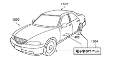
図18は、本実施形態に係る移動体として、自動車1500を模式的に示す斜視図である。   FIG. 18 is a perspective view schematically showing an automobile 1500 as a moving body according to the present embodiment.

自動車1500には、物理量検出装置400が内蔵されている。具体的には、図18に示すように、自動車1500の車体1502には、自動車1500の角速度を検知する振動素子100を内蔵してエンジンの出力を制御する電子制御ユニット(ECU:Electronic Control Unit)1504が搭載されている。また、物理量検出装置400は、他にも、車体姿勢制御ユニット、アンチロックブレーキシステム(ABS)、エアバック、タイヤ・プレッシャー・モニタリング・システム(TPMS:Tire Pressure Monitoring System)、に広く適用することができる。   The automobile 1500 has a physical quantity detection device 400 built therein. Specifically, as shown in FIG. 18, an electronic control unit (ECU) that controls an engine output by incorporating a vibration element 100 that detects an angular velocity of the automobile 1500 in a vehicle body 1502 of the automobile 1500. 1504 is mounted. In addition, the physical quantity detection device 400 can be widely applied to a vehicle body attitude control unit, an anti-lock brake system (ABS), an air bag, and a tire pressure monitoring system (TPMS). it can.

本実施形態に係る移動体では、検出精度の高い物理量検出装置400を含む。したがって、本実施形態に係る移動体は、良好な特性を有することができる。   The moving body according to the present embodiment includes a physical quantity detection device 400 with high detection accuracy. Therefore, the moving body according to the present embodiment can have good characteristics.

本発明は本実施形態に限定されず、本発明の要旨の範囲内で種々の変形実施が可能である。   The present invention is not limited to the present embodiment, and various modifications can be made within the scope of the gist of the present invention.

例えば、振動素子100の振動片1は、H型やダブルT型以外にも、例えば、音叉型やくし歯型であってもよいし、三角柱、四角柱、円柱状等の形状の音片型であってもよいし、三脚型であってもよい。   For example, the resonator element 1 of the resonator element 100 may be, for example, a tuning fork type or a comb-teeth type other than the H type or the double T type, or a sound piece type such as a triangular prism, a quadrangular prism, or a cylindrical shape. There may be a tripod type.

また、振動片1の材料としては、水晶(SiO)、タンタル酸リチウム(LiTaO)、ニオブ酸リチウム(LiNbO)等の圧電単結晶の圧電材料に限らず、ジルコン酸チタン酸鉛(PZT)等の圧電セラミックスなどの圧電性材料を用いてもよい。 The material of the resonator element 1 is not limited to a piezoelectric single crystal piezoelectric material such as quartz (SiO 2 ), lithium tantalate (LiTaO 3 ), lithium niobate (LiNbO 3 ), etc., but also lead zirconate titanate (PZT). Piezoelectric materials such as piezoelectric ceramics may be used.

また、振動素子100は、例えば、振動片1をシリコン半導体で構成し、振動片1(シリコン半導体)の表面の一部に、電極に挟まれた酸化亜鉛(ZnO)、窒化アルミニウム(AlN)等の圧電薄膜を配置した構造であってもよい。   In the resonator element 100, for example, the resonator element 1 is made of a silicon semiconductor, and zinc oxide (ZnO), aluminum nitride (AlN), or the like sandwiched between electrodes on a part of the surface of the resonator element 1 (silicon semiconductor). The structure which arrange | positioned the piezoelectric thin film may be sufficient.

また、振動素子100は、圧電型の振動素子以外にも、動電型、静電容量型(シリコンMEMS等)、渦電流型、光学型、ひずみゲージ型等の振動素子であってもよい。   The vibration element 100 may be a vibration element such as an electrodynamic type, a capacitance type (silicon MEMS, etc.), an eddy current type, an optical type, and a strain gauge type, in addition to the piezoelectric type vibration element.

また、振動素子100が検出する物理量は、角速度に限らず、角加速度、加速度、速度、力などであってもよい。すなわち、検出回路450あるいは物理量検出装置400は、角速度に限らず、角加速度、加速度、速度、力などの大きさに応じた信号を出力するものであってもよい。   Further, the physical quantity detected by the vibration element 100 is not limited to angular velocity, but may be angular acceleration, acceleration, velocity, force, or the like. That is, the detection circuit 450 or the physical quantity detection device 400 is not limited to the angular velocity, and may output a signal corresponding to the magnitude of angular acceleration, acceleration, velocity, force, and the like.

上述した実施形態および変形例は一例であって、これらに限定されるわけではない。例えば、各実施形態および各変形例を適宜組み合わせることも可能である。   The above-described embodiments and modifications are merely examples, and the present invention is not limited to these. For example, it is possible to appropriately combine each embodiment and each modification.

本発明は、実施の形態で説明した構成と実質的に同一の構成(例えば、機能、方法及び結果が同一の構成、あるいは目的及び効果が同一の構成)を含む。また、本発明は、実施の形態で説明した構成の本質的でない部分を置き換えた構成を含む。また、本発明は、実施の形態で説明した構成と同一の作用効果を奏する構成又は同一の目的を達成することができる構成を含む。また、本発明は、実施の形態で説明した構成に公知技術を付加した構成を含む。   The present invention includes configurations that are substantially the same as the configurations described in the embodiments (for example, configurations that have the same functions, methods, and results, or configurations that have the same objects and effects). In addition, the invention includes a configuration in which a non-essential part of the configuration described in the embodiment is replaced. In addition, the present invention includes a configuration that exhibits the same operational effects as the configuration described in the embodiment or a configuration that can achieve the same object. Further, the invention includes a configuration in which a known technique is added to the configuration described in the embodiment.

1…振動片、2a…第1主面、2b…第2主面、3…側面、5…幅広部、10…基部、30…駆動入力電極、32…駆動出力電極、40…第1検出電極、42…第2検出電極、44…第3検出電極、46…第4検出電極、50…駆動入力配線、50a…端子部、52…駆動出力配線、52a…端子部、60…第1検出配線、60a…端子部、62…第2検出配線、62a…端子部、64…第3検出配線、64a…端子部、66…第4検出配線、66a…端子部、70…固定電位配線、70a…端子部、100…振動素子、210…第1連結腕、212…第2連結腕、220…第1駆動振動腕、222…第2駆動振動腕、224…第3駆動振動腕、226…第4駆動振動腕、230…第1検出振動腕、231…貫通孔、232…第2検出振動腕、233…貫通孔、240…第1支持部、242…第2支持部、250…第1梁部、252…第2梁部、254…第3梁部、256…第4梁部、260…第1駆動検出振動腕、262…第2駆動検出振動腕、300…実装基板、400…物理量検出装置、440…駆動回路、441…I/V変換回路、442…AC増幅回路、443…振幅調整回路、450…検出回路、451,452…チャージアンプ、453…差動増幅回路、454…フィルター回路、455…AC増幅回路、456…同期検波回路、457…平滑回路、458…可変増幅回路、459…フィルター回路、1100…パーソナルコンピューター、1102…キーボード、1104…本体部、1106…表示ユニット、1108…表示部、1200…携帯電話機、1202…操作ボタン、1204…受話口、1206…送話口、1208…表示部、1300…デジタルスチルカメラ、1302…ケース、1304…受光ユニット、1306…シャッターボタン、1308…メモリー、1310…表示部、1312…ビデオ信号出力端子、1314…入出力端子、1430…テレビモニター、1440…パーソナルコンピューター、1500…自動車、1502…車体 DESCRIPTION OF SYMBOLS 1 ... Vibrating piece, 2a ... 1st main surface, 2b ... 2nd main surface, 3 ... Side surface, 5 ... Wide part, 10 ... Base part, 30 ... Drive input electrode, 32 ... Drive output electrode, 40 ... 1st detection electrode , 42 ... second detection electrode, 44 ... third detection electrode, 46 ... fourth detection electrode, 50 ... drive input wiring, 50a ... terminal portion, 52 ... drive output wiring, 52a ... terminal portion, 60 ... first detection wiring , 60a ... terminal portion, 62 ... second detection wiring, 62a ... terminal portion, 64 ... third detection wiring, 64a ... terminal portion, 66 ... fourth detection wiring, 66a ... terminal portion, 70 ... fixed potential wiring, 70a ... Terminal part 100 ... Vibrating element 210 ... First connecting arm 212 ... Second connecting arm 220 ... First driving vibrating arm 222 ... Second driving vibrating arm 224 ... Third driving vibrating arm 226 ... Four Drive vibration arm, 230 ... first detection vibration arm, 231 ... through hole, 232 ... second detection vibration arm 233 ... through hole, 240 ... first support portion, 242 ... second support portion, 250 ... first beam portion, 252 ... second beam portion, 254 ... third beam portion, 256 ... fourth beam portion, 260 ... first DESCRIPTION OF SYMBOLS 1 drive detection vibration arm, 262 ... 2nd drive detection vibration arm, 300 ... Mounting board, 400 ... Physical quantity detection apparatus, 440 ... Drive circuit, 441 ... I / V conversion circuit, 442 ... AC amplification circuit, 443 ... Amplitude adjustment circuit 450, detection circuit, 451, 452 ... charge amplifier, 453 ... differential amplification circuit, 454 ... filter circuit, 455 ... AC amplification circuit, 456 ... synchronous detection circuit, 457 ... smoothing circuit, 458 ... variable amplification circuit, 459 ... Filter circuit, 1100 ... personal computer, 1102 ... keyboard, 1104 ... main body, 1106 ... display unit, 1108 ... display unit, 1200 ... mobile phone, 1202 Operation buttons, 1204 ... Earpiece, 1206 ... Mouthpiece, 1208 ... Display, 1300 ... Digital still camera, 1302 ... Case, 1304 ... Light receiving unit, 1306 ... Shutter button, 1308 ... Memory, 1310 ... Display, 1312 ... Video signal output terminal, 1314 ... Input / output terminal, 1430 ... TV monitor, 1440 ... Personal computer, 1500 ... Automobile, 1502 ... Car body

Claims (8)

振動素子を駆動する駆動信号に基づいて前記振動素子の出力信号に含まれる物理量に応じた信号を検波する検波部と、
前記検波部よりも前段に設けられたフィルター部と、を含み、
前記フィルター部は、
カットオフ周波数が、前記振動素子の駆動モードの共振周波数と検出モードの共振周波数との間にあり、通過帯域に前記駆動モードの共振周波数を含む、物理量検出用回路。
A detector for detecting a signal corresponding to a physical quantity included in the output signal of the vibration element based on a drive signal for driving the vibration element;
Including a filter unit provided at a stage prior to the detection unit,
The filter section is
A physical quantity detection circuit, wherein a cutoff frequency is between a resonance frequency of a driving mode and a detection mode of the vibration element, and the resonance frequency of the driving mode is included in a pass band.
前記駆動モードの前記共振周波数が前記検出モードの前記共振周波数よりも低く、
前記フィルター部は、
カットオフ周波数が前記検出モードの前記共振周波数よりも低いローパスフィルターである、請求項1に記載の物理量検出用回路。
The resonance frequency of the drive mode is lower than the resonance frequency of the detection mode;
The filter section is
The physical quantity detection circuit according to claim 1, wherein the physical quantity detection circuit is a low-pass filter having a cutoff frequency lower than the resonance frequency of the detection mode.
前記駆動モードの前記共振周波数が前記検出モードの前記共振周波数よりも高く、
前記フィルター部は、
カットオフ周波数が前記検出モードの前記共振周波数よりも高いハイパスフィルターである、請求項1に記載の物理量検出用回路。
The resonance frequency of the drive mode is higher than the resonance frequency of the detection mode;
The filter section is
The physical quantity detection circuit according to claim 1, which is a high-pass filter having a cutoff frequency higher than the resonance frequency of the detection mode.
前記振動素子の出力信号を差動増幅する差動増幅部と、
前記差動増幅部と前記検波部との間に設けられている交流増幅部と、を含み、
前記フィルター部は、
前記差動増幅部と前記交流増幅部との間に設けられている、請求項1乃至3のいずれか一項に記載の物理量検出用回路。
A differential amplifier for differentially amplifying the output signal of the vibrating element;
An AC amplification unit provided between the differential amplification unit and the detection unit,
The filter section is
The physical quantity detection circuit according to claim 1, which is provided between the differential amplification unit and the AC amplification unit.
前記振動素子の出力信号を差動増幅する差動増幅部と、
前記差動増幅部と前記検波部との間に設けられている交流増幅部と、を含み、
前記フィルター部は、
前記交流増幅部と前記検波部との間に設けられている、請求項1乃至3のいずれか一項に記載の物理量検出用回路。
A differential amplifier for differentially amplifying the output signal of the vibrating element;
An AC amplification unit provided between the differential amplification unit and the detection unit,
The filter section is
4. The physical quantity detection circuit according to claim 1, wherein the physical quantity detection circuit is provided between the AC amplification unit and the detection unit. 5.
請求項1乃至5のいずれか一項に記載の物理量検出用回路と、前記振動素子と、を含む、物理量検出装置。   A physical quantity detection device comprising the physical quantity detection circuit according to claim 1 and the vibration element. 請求項1乃至5のいずれか一項に記載の物理量検出用回路、又は、請求項6に記載の物理量検出装置を含む、電子機器。   An electronic apparatus comprising the physical quantity detection circuit according to any one of claims 1 to 5 or the physical quantity detection device according to claim 6. 請求項1乃至5のいずれか一項に記載の物理量検出用回路、又は、請求項6に記載の物理量検出装置を含む、移動体。   A moving body comprising the physical quantity detection circuit according to claim 1 or the physical quantity detection device according to claim 6.
JP2014061547A 2014-03-25 2014-03-25 Physical quantity detection circuit, physical quantity detection device, electronic apparatus, and mobile entity Withdrawn JP2015184157A (en)

Priority Applications (3)

Application Number Priority Date Filing Date Title
JP2014061547A JP2015184157A (en) 2014-03-25 2014-03-25 Physical quantity detection circuit, physical quantity detection device, electronic apparatus, and mobile entity
US14/666,679 US20150276404A1 (en) 2014-03-25 2015-03-24 Physical quantity detection circuit, physical quantity detecting device, electronic apparatus, and moving object
CN201510134545.6A CN104949665A (en) 2014-03-25 2015-03-25 Physical quantity detection circuit, physical quantity detection device, electronic device, and moving object

Applications Claiming Priority (1)

Application Number Priority Date Filing Date Title
JP2014061547A JP2015184157A (en) 2014-03-25 2014-03-25 Physical quantity detection circuit, physical quantity detection device, electronic apparatus, and mobile entity

Publications (2)

Publication Number Publication Date
JP2015184157A true JP2015184157A (en) 2015-10-22
JP2015184157A5 JP2015184157A5 (en) 2017-04-06

Family

ID=54164512

Family Applications (1)

Application Number Title Priority Date Filing Date
JP2014061547A Withdrawn JP2015184157A (en) 2014-03-25 2014-03-25 Physical quantity detection circuit, physical quantity detection device, electronic apparatus, and mobile entity

Country Status (3)

Country Link
US (1) US20150276404A1 (en)
JP (1) JP2015184157A (en)
CN (1) CN104949665A (en)

Cited By (1)

* Cited by examiner, † Cited by third party
Publication number Priority date Publication date Assignee Title
DE112016004227T5 (en) 2015-09-17 2018-06-14 Ntn Corporation Double row self-aligning roller bearing

Families Citing this family (8)

* Cited by examiner, † Cited by third party
Publication number Priority date Publication date Assignee Title
JP6399283B2 (en) * 2014-03-24 2018-10-03 セイコーエプソン株式会社 Physical quantity detection device, electronic device, and moving object
JP6507565B2 (en) * 2014-10-28 2019-05-08 セイコーエプソン株式会社 Electronic device, electronic device and mobile
JP6477101B2 (en) * 2015-03-23 2019-03-06 セイコーエプソン株式会社 Angular velocity detecting element, angular velocity detecting device, electronic device and moving body
JP6477100B2 (en) * 2015-03-23 2019-03-06 セイコーエプソン株式会社 Angular velocity detecting element, angular velocity detecting device, electronic device and moving body
JP6693214B2 (en) * 2016-03-25 2020-05-13 セイコーエプソン株式会社 Physical quantity detection device, electronic device and moving body
EP3842742B1 (en) * 2018-09-28 2023-09-13 Kyocera Corporation Sensor element and angular velocity sensor
JP7183902B2 (en) 2019-03-25 2022-12-06 セイコーエプソン株式会社 Vibration devices, electronic equipment and moving objects
CN111189490A (en) * 2019-11-15 2020-05-22 陕西飞机工业(集团)有限公司 Aircraft environment monitoring system

Citations (6)

* Cited by examiner, † Cited by third party
Publication number Priority date Publication date Assignee Title
JPS612013A (en) * 1984-06-14 1986-01-08 Nippon Denso Co Ltd Angular velocity sensor
US4930351A (en) * 1988-03-24 1990-06-05 Wjm Corporation Vibratory linear acceleration and angular rate sensing system
JP2003021516A (en) * 2001-07-06 2003-01-24 Ngk Insulators Ltd Physical quantity measuring device
JP2008070333A (en) * 2006-09-15 2008-03-27 Denso Corp Oscillation-type angular velocity sensor and vehicle control system
JP2008256668A (en) * 2007-03-09 2008-10-23 Matsushita Electric Ind Co Ltd Angular velocity sensor
WO2010092816A1 (en) * 2009-02-13 2010-08-19 パナソニック株式会社 Oscillator circuit, method for manufacturing oscillator circuit, inertial sensor using the oscillator circuit, and electronic device

Family Cites Families (3)

* Cited by examiner, † Cited by third party
Publication number Priority date Publication date Assignee Title
CN201688848U (en) * 2010-05-28 2010-12-29 南京理工大学 Interface circuit of dual mass vibration type silicon micromechanical gyroscope
CN102620726B (en) * 2012-04-04 2014-10-29 西北工业大学 Double-closed-loop control circuit of micromechanical gyroscope
US9109894B2 (en) * 2013-04-26 2015-08-18 Maxim Integrated Products, Inc. Gyroscope shock and disturbance detection circuit

Patent Citations (6)

* Cited by examiner, † Cited by third party
Publication number Priority date Publication date Assignee Title
JPS612013A (en) * 1984-06-14 1986-01-08 Nippon Denso Co Ltd Angular velocity sensor
US4930351A (en) * 1988-03-24 1990-06-05 Wjm Corporation Vibratory linear acceleration and angular rate sensing system
JP2003021516A (en) * 2001-07-06 2003-01-24 Ngk Insulators Ltd Physical quantity measuring device
JP2008070333A (en) * 2006-09-15 2008-03-27 Denso Corp Oscillation-type angular velocity sensor and vehicle control system
JP2008256668A (en) * 2007-03-09 2008-10-23 Matsushita Electric Ind Co Ltd Angular velocity sensor
WO2010092816A1 (en) * 2009-02-13 2010-08-19 パナソニック株式会社 Oscillator circuit, method for manufacturing oscillator circuit, inertial sensor using the oscillator circuit, and electronic device

Cited By (1)

* Cited by examiner, † Cited by third party
Publication number Priority date Publication date Assignee Title
DE112016004227T5 (en) 2015-09-17 2018-06-14 Ntn Corporation Double row self-aligning roller bearing

Also Published As

Publication number Publication date
CN104949665A (en) 2015-09-30
US20150276404A1 (en) 2015-10-01

Similar Documents

Publication Publication Date Title
US10794778B2 (en) Physical quantity detecting device, electronic apparatus, and moving object
JP2015184157A (en) Physical quantity detection circuit, physical quantity detection device, electronic apparatus, and mobile entity
US9379307B2 (en) Vibrator element, vibrator, electronic device, electronic apparatus, and moving object
JP6582501B2 (en) Vibration element, vibrator, electronic device and moving body
US9995582B2 (en) Vibrating element, vibrating device, electronic apparatus, and moving object
US10088314B2 (en) Angular velocity detection element, angular velocity detection device, electronic apparatus, and moving object
JP6623682B2 (en) Physical quantity detection vibrating piece, physical quantity detection device, electronic equipment and moving object
JP2015184009A (en) Vibration element, electronic apparatus, and mobile entity
US20160282117A1 (en) Angular velocity detection element, angular velocity detection device, electronic apparatus, and moving object
JP2016085192A (en) Vibration element, electronic device, electronic apparatus and movable body
JP2015090275A (en) Manufacturing method of vibration element
JP2015001420A (en) Gyro sensor element, gyro device, electronic device, and mobile
JP2016176893A (en) Angular velocity detection element, angular velocity detection device, electronic apparatus and mobile body
JP2015203583A (en) Oscillation element, electronic device and moving body
JP6264535B2 (en) Vibration element manufacturing substrate, vibration element manufacturing method, physical quantity detection device, electronic device, and moving body
JP2014092500A (en) Vibration piece, vibrator, electronic device, electronic apparatus, and mobile body
JP2017090398A (en) Vibration piece, vibration device, electronic apparatus and movable body
JP6680079B2 (en) Electronic device, manufacturing method of electronic device, physical quantity sensor, electronic device and moving body
JP2016186479A (en) Physical quantity detection vibration element, physical quantity detection vibrator, electronic apparatus and mobile body
JP2015169492A (en) Electronic device, signal detection method of electronic device, electronic apparatus and moving body
JP6641874B2 (en) Physical quantity detection device, electronic equipment and moving object
JP2015087251A (en) Vibration element, physical quantity detection device, electronic apparatus and movable body
JP2016061710A (en) Vibration element, gyro element, electronic device, electronic equipment, and mobile body
JP2014178165A (en) Vibration element, transducer, electronic device, electronic apparatus, and mobile body
JP2015169648A (en) Functional element, electronic device, physical quantity detection apparatus, electronic apparatus, and mobile body

Legal Events

Date Code Title Description
RD04 Notification of resignation of power of attorney

Free format text: JAPANESE INTERMEDIATE CODE: A7424

Effective date: 20160617

RD03 Notification of appointment of power of attorney

Free format text: JAPANESE INTERMEDIATE CODE: A7423

Effective date: 20160624

A521 Request for written amendment filed

Free format text: JAPANESE INTERMEDIATE CODE: A523

Effective date: 20170301

A621 Written request for application examination

Free format text: JAPANESE INTERMEDIATE CODE: A621

Effective date: 20170301

A131 Notification of reasons for refusal

Free format text: JAPANESE INTERMEDIATE CODE: A131

Effective date: 20171226

A977 Report on retrieval

Free format text: JAPANESE INTERMEDIATE CODE: A971007

Effective date: 20171227

A761 Written withdrawal of application

Free format text: JAPANESE INTERMEDIATE CODE: A761

Effective date: 20180221