JP7147570B2 - Semiconductor laminate and light receiving element - Google Patents
Semiconductor laminate and light receiving element Download PDFInfo
- Publication number
- JP7147570B2 JP7147570B2 JP2019004259A JP2019004259A JP7147570B2 JP 7147570 B2 JP7147570 B2 JP 7147570B2 JP 2019004259 A JP2019004259 A JP 2019004259A JP 2019004259 A JP2019004259 A JP 2019004259A JP 7147570 B2 JP7147570 B2 JP 7147570B2
- Authority
- JP
- Japan
- Prior art keywords
- layer
- buffer layer
- concentration
- semiconductor laminate
- receiving element
- Prior art date
- Legal status (The legal status is an assumption and is not a legal conclusion. Google has not performed a legal analysis and makes no representation as to the accuracy of the status listed.)
- Active
Links
- 239000004065 semiconductor Substances 0.000 title claims description 100
- 239000000758 substrate Substances 0.000 claims description 59
- 238000010521 absorption reaction Methods 0.000 claims description 31
- 229910000530 Gallium indium arsenide Inorganic materials 0.000 claims description 26
- 150000001875 compounds Chemical class 0.000 claims description 18
- 238000000034 method Methods 0.000 claims description 14
- 229910001218 Gallium arsenide Inorganic materials 0.000 claims description 13
- 238000009826 distribution Methods 0.000 claims description 9
- GPXJNWSHGFTCBW-UHFFFAOYSA-N Indium phosphide Chemical compound [In]#P GPXJNWSHGFTCBW-UHFFFAOYSA-N 0.000 description 27
- 239000012535 impurity Substances 0.000 description 19
- 238000002161 passivation Methods 0.000 description 18
- 239000007789 gas Substances 0.000 description 17
- 238000004519 manufacturing process Methods 0.000 description 17
- 239000000463 material Substances 0.000 description 13
- 230000015572 biosynthetic process Effects 0.000 description 12
- JBRZTFJDHDCESZ-UHFFFAOYSA-N AsGa Chemical compound [As]#[Ga] JBRZTFJDHDCESZ-UHFFFAOYSA-N 0.000 description 11
- 238000009792 diffusion process Methods 0.000 description 9
- 238000005229 chemical vapour deposition Methods 0.000 description 8
- 238000001004 secondary ion mass spectrometry Methods 0.000 description 8
- 238000000927 vapour-phase epitaxy Methods 0.000 description 8
- 239000010931 gold Substances 0.000 description 7
- 239000002994 raw material Substances 0.000 description 7
- 239000011701 zinc Substances 0.000 description 7
- 238000005259 measurement Methods 0.000 description 6
- RGGPNXQUMRMPRA-UHFFFAOYSA-N triethylgallium Chemical compound CC[Ga](CC)CC RGGPNXQUMRMPRA-UHFFFAOYSA-N 0.000 description 5
- IBEFSUTVZWZJEL-UHFFFAOYSA-N trimethylindium Chemical compound C[In](C)C IBEFSUTVZWZJEL-UHFFFAOYSA-N 0.000 description 5
- -1 TMGa ( For example Chemical compound 0.000 description 4
- 239000013078 crystal Substances 0.000 description 4
- BASFCYQUMIYNBI-UHFFFAOYSA-N platinum Substances [Pt] BASFCYQUMIYNBI-UHFFFAOYSA-N 0.000 description 4
- 230000035945 sensitivity Effects 0.000 description 4
- VCZQFJFZMMALHB-UHFFFAOYSA-N tetraethylsilane Chemical compound CC[Si](CC)(CC)CC VCZQFJFZMMALHB-UHFFFAOYSA-N 0.000 description 4
- HTDIUWINAKAPER-UHFFFAOYSA-N trimethylarsine Chemical compound C[As](C)C HTDIUWINAKAPER-UHFFFAOYSA-N 0.000 description 4
- 101100208382 Danio rerio tmsb gene Proteins 0.000 description 3
- 229910005542 GaSb Inorganic materials 0.000 description 3
- 229910000673 Indium arsenide Inorganic materials 0.000 description 3
- 229910052581 Si3N4 Inorganic materials 0.000 description 3
- BLRPTPMANUNPDV-UHFFFAOYSA-N Silane Chemical compound [SiH4] BLRPTPMANUNPDV-UHFFFAOYSA-N 0.000 description 3
- KXNLCSXBJCPWGL-UHFFFAOYSA-N [Ga].[As].[In] Chemical compound [Ga].[As].[In] KXNLCSXBJCPWGL-UHFFFAOYSA-N 0.000 description 3
- 238000004458 analytical method Methods 0.000 description 3
- 230000000903 blocking effect Effects 0.000 description 3
- 239000004020 conductor Substances 0.000 description 3
- 230000000694 effects Effects 0.000 description 3
- PCHJSUWPFVWCPO-UHFFFAOYSA-N gold Chemical compound [Au] PCHJSUWPFVWCPO-UHFFFAOYSA-N 0.000 description 3
- 229910052737 gold Inorganic materials 0.000 description 3
- RPQDHPTXJYYUPQ-UHFFFAOYSA-N indium arsenide Chemical compound [In]#[As] RPQDHPTXJYYUPQ-UHFFFAOYSA-N 0.000 description 3
- 229910052751 metal Inorganic materials 0.000 description 3
- 239000002184 metal Substances 0.000 description 3
- 238000012986 modification Methods 0.000 description 3
- 230000004048 modification Effects 0.000 description 3
- PXHVJJICTQNCMI-UHFFFAOYSA-N nickel Substances [Ni] PXHVJJICTQNCMI-UHFFFAOYSA-N 0.000 description 3
- 229910000077 silane Inorganic materials 0.000 description 3
- HQVNEWCFYHHQES-UHFFFAOYSA-N silicon nitride Chemical compound N12[Si]34N5[Si]62N3[Si]51N64 HQVNEWCFYHHQES-UHFFFAOYSA-N 0.000 description 3
- QTQRGDBFHFYIBH-UHFFFAOYSA-N tert-butylarsenic Chemical compound CC(C)(C)[As] QTQRGDBFHFYIBH-UHFFFAOYSA-N 0.000 description 3
- 239000010936 titanium Substances 0.000 description 3
- OTRPZROOJRIMKW-UHFFFAOYSA-N triethylindigane Chemical compound CC[In](CC)CC OTRPZROOJRIMKW-UHFFFAOYSA-N 0.000 description 3
- GYHNNYVSQQEPJS-UHFFFAOYSA-N Gallium Chemical compound [Ga] GYHNNYVSQQEPJS-UHFFFAOYSA-N 0.000 description 2
- VYPSYNLAJGMNEJ-UHFFFAOYSA-N Silicium dioxide Chemical compound O=[Si]=O VYPSYNLAJGMNEJ-UHFFFAOYSA-N 0.000 description 2
- 229910052787 antimony Inorganic materials 0.000 description 2
- WATWJIUSRGPENY-UHFFFAOYSA-N antimony atom Chemical compound [Sb] WATWJIUSRGPENY-UHFFFAOYSA-N 0.000 description 2
- NWAIGJYBQQYSPW-UHFFFAOYSA-N azanylidyneindigane Chemical compound [In]#N NWAIGJYBQQYSPW-UHFFFAOYSA-N 0.000 description 2
- 229910052792 caesium Inorganic materials 0.000 description 2
- 238000002474 experimental method Methods 0.000 description 2
- 229910052733 gallium Inorganic materials 0.000 description 2
- 238000010438 heat treatment Methods 0.000 description 2
- 239000012212 insulator Substances 0.000 description 2
- UIUXUFNYAYAMOE-UHFFFAOYSA-N methylsilane Chemical compound [SiH3]C UIUXUFNYAYAMOE-UHFFFAOYSA-N 0.000 description 2
- 238000001451 molecular beam epitaxy Methods 0.000 description 2
- 229910052814 silicon oxide Inorganic materials 0.000 description 2
- ZGNPLWZYVAFUNZ-UHFFFAOYSA-N tert-butylphosphane Chemical compound CC(C)(C)P ZGNPLWZYVAFUNZ-UHFFFAOYSA-N 0.000 description 2
- OKTJSMMVPCPJKN-UHFFFAOYSA-N Carbon Chemical compound [C] OKTJSMMVPCPJKN-UHFFFAOYSA-N 0.000 description 1
- UFHFLCQGNIYNRP-UHFFFAOYSA-N Hydrogen Chemical compound [H][H] UFHFLCQGNIYNRP-UHFFFAOYSA-N 0.000 description 1
- NINIDFKCEFEMDL-UHFFFAOYSA-N Sulfur Chemical compound [S] NINIDFKCEFEMDL-UHFFFAOYSA-N 0.000 description 1
- RTAQQCXQSZGOHL-UHFFFAOYSA-N Titanium Chemical compound [Ti] RTAQQCXQSZGOHL-UHFFFAOYSA-N 0.000 description 1
- HCHKCACWOHOZIP-UHFFFAOYSA-N Zinc Chemical compound [Zn] HCHKCACWOHOZIP-UHFFFAOYSA-N 0.000 description 1
- 230000001133 acceleration Effects 0.000 description 1
- RBFQJDQYXXHULB-UHFFFAOYSA-N arsane Chemical compound [AsH3] RBFQJDQYXXHULB-UHFFFAOYSA-N 0.000 description 1
- QVGXLLKOCUKJST-UHFFFAOYSA-N atomic oxygen Chemical compound [O] QVGXLLKOCUKJST-UHFFFAOYSA-N 0.000 description 1
- 229910052799 carbon Inorganic materials 0.000 description 1
- 238000004140 cleaning Methods 0.000 description 1
- 230000003749 cleanliness Effects 0.000 description 1
- 230000000295 complement effect Effects 0.000 description 1
- 230000007423 decrease Effects 0.000 description 1
- HQWPLXHWEZZGKY-UHFFFAOYSA-N diethylzinc Chemical compound CC[Zn]CC HQWPLXHWEZZGKY-UHFFFAOYSA-N 0.000 description 1
- AXAZMDOAUQTMOW-UHFFFAOYSA-N dimethylzinc Chemical compound C[Zn]C AXAZMDOAUQTMOW-UHFFFAOYSA-N 0.000 description 1
- 238000005516 engineering process Methods 0.000 description 1
- 238000005530 etching Methods 0.000 description 1
- 229910052732 germanium Inorganic materials 0.000 description 1
- GNPVGFCGXDBREM-UHFFFAOYSA-N germanium atom Chemical compound [Ge] GNPVGFCGXDBREM-UHFFFAOYSA-N 0.000 description 1
- 229910021478 group 5 element Inorganic materials 0.000 description 1
- 150000004678 hydrides Chemical class 0.000 description 1
- 239000001257 hydrogen Substances 0.000 description 1
- 229910052739 hydrogen Inorganic materials 0.000 description 1
- 229910044991 metal oxide Inorganic materials 0.000 description 1
- 150000004706 metal oxides Chemical class 0.000 description 1
- 229910052759 nickel Inorganic materials 0.000 description 1
- 229910052760 oxygen Inorganic materials 0.000 description 1
- 239000001301 oxygen Substances 0.000 description 1
- 230000000149 penetrating effect Effects 0.000 description 1
- 229910052697 platinum Inorganic materials 0.000 description 1
- 238000002360 preparation method Methods 0.000 description 1
- 229910052710 silicon Inorganic materials 0.000 description 1
- 239000010703 silicon Substances 0.000 description 1
- 238000004544 sputter deposition Methods 0.000 description 1
- 229910052717 sulfur Inorganic materials 0.000 description 1
- 239000011593 sulfur Substances 0.000 description 1
- 229910052719 titanium Inorganic materials 0.000 description 1
- RBEXEKTWBGMBDZ-UHFFFAOYSA-N tri(propan-2-yl)stibane Chemical compound CC(C)[Sb](C(C)C)C(C)C RBEXEKTWBGMBDZ-UHFFFAOYSA-N 0.000 description 1
- KKOFCVMVBJXDFP-UHFFFAOYSA-N triethylstibane Chemical compound CC[Sb](CC)CC KKOFCVMVBJXDFP-UHFFFAOYSA-N 0.000 description 1
- PORFVJURJXKREL-UHFFFAOYSA-N trimethylstibine Chemical compound C[Sb](C)C PORFVJURJXKREL-UHFFFAOYSA-N 0.000 description 1
- 238000007740 vapor deposition Methods 0.000 description 1
- 229910052725 zinc Inorganic materials 0.000 description 1
Images


Classifications
-
- H—ELECTRICITY
- H01—ELECTRIC ELEMENTS
- H01L—SEMICONDUCTOR DEVICES NOT COVERED BY CLASS H10
- H01L31/00—Semiconductor devices sensitive to infrared radiation, light, electromagnetic radiation of shorter wavelength or corpuscular radiation and specially adapted either for the conversion of the energy of such radiation into electrical energy or for the control of electrical energy by such radiation; Processes or apparatus specially adapted for the manufacture or treatment thereof or of parts thereof; Details thereof
- H01L31/0248—Semiconductor devices sensitive to infrared radiation, light, electromagnetic radiation of shorter wavelength or corpuscular radiation and specially adapted either for the conversion of the energy of such radiation into electrical energy or for the control of electrical energy by such radiation; Processes or apparatus specially adapted for the manufacture or treatment thereof or of parts thereof; Details thereof characterised by their semiconductor bodies
- H01L31/0352—Semiconductor devices sensitive to infrared radiation, light, electromagnetic radiation of shorter wavelength or corpuscular radiation and specially adapted either for the conversion of the energy of such radiation into electrical energy or for the control of electrical energy by such radiation; Processes or apparatus specially adapted for the manufacture or treatment thereof or of parts thereof; Details thereof characterised by their semiconductor bodies characterised by their shape or by the shapes, relative sizes or disposition of the semiconductor regions
- H01L31/035236—Superlattices; Multiple quantum well structures
-
- H—ELECTRICITY
- H01—ELECTRIC ELEMENTS
- H01L—SEMICONDUCTOR DEVICES NOT COVERED BY CLASS H10
- H01L21/00—Processes or apparatus adapted for the manufacture or treatment of semiconductor or solid state devices or of parts thereof
- H01L21/02—Manufacture or treatment of semiconductor devices or of parts thereof
- H01L21/02104—Forming layers
- H01L21/02365—Forming inorganic semiconducting materials on a substrate
- H01L21/02367—Substrates
- H01L21/0237—Materials
- H01L21/02387—Group 13/15 materials
- H01L21/02392—Phosphides
-
- H—ELECTRICITY
- H01—ELECTRIC ELEMENTS
- H01L—SEMICONDUCTOR DEVICES NOT COVERED BY CLASS H10
- H01L21/00—Processes or apparatus adapted for the manufacture or treatment of semiconductor or solid state devices or of parts thereof
- H01L21/02—Manufacture or treatment of semiconductor devices or of parts thereof
- H01L21/02104—Forming layers
- H01L21/02365—Forming inorganic semiconducting materials on a substrate
- H01L21/02436—Intermediate layers between substrates and deposited layers
- H01L21/02439—Materials
- H01L21/02455—Group 13/15 materials
- H01L21/02461—Phosphides
-
- H—ELECTRICITY
- H01—ELECTRIC ELEMENTS
- H01L—SEMICONDUCTOR DEVICES NOT COVERED BY CLASS H10
- H01L21/00—Processes or apparatus adapted for the manufacture or treatment of semiconductor or solid state devices or of parts thereof
- H01L21/02—Manufacture or treatment of semiconductor devices or of parts thereof
- H01L21/02104—Forming layers
- H01L21/02365—Forming inorganic semiconducting materials on a substrate
- H01L21/02436—Intermediate layers between substrates and deposited layers
- H01L21/02439—Materials
- H01L21/02455—Group 13/15 materials
- H01L21/02463—Arsenides
-
- H—ELECTRICITY
- H01—ELECTRIC ELEMENTS
- H01L—SEMICONDUCTOR DEVICES NOT COVERED BY CLASS H10
- H01L21/00—Processes or apparatus adapted for the manufacture or treatment of semiconductor or solid state devices or of parts thereof
- H01L21/02—Manufacture or treatment of semiconductor devices or of parts thereof
- H01L21/02104—Forming layers
- H01L21/02365—Forming inorganic semiconducting materials on a substrate
- H01L21/02436—Intermediate layers between substrates and deposited layers
- H01L21/02439—Materials
- H01L21/02455—Group 13/15 materials
- H01L21/02466—Antimonides
-
- H—ELECTRICITY
- H01—ELECTRIC ELEMENTS
- H01L—SEMICONDUCTOR DEVICES NOT COVERED BY CLASS H10
- H01L21/00—Processes or apparatus adapted for the manufacture or treatment of semiconductor or solid state devices or of parts thereof
- H01L21/02—Manufacture or treatment of semiconductor devices or of parts thereof
- H01L21/02104—Forming layers
- H01L21/02365—Forming inorganic semiconducting materials on a substrate
- H01L21/02436—Intermediate layers between substrates and deposited layers
- H01L21/02494—Structure
- H01L21/02496—Layer structure
- H01L21/02502—Layer structure consisting of two layers
-
- H—ELECTRICITY
- H01—ELECTRIC ELEMENTS
- H01L—SEMICONDUCTOR DEVICES NOT COVERED BY CLASS H10
- H01L21/00—Processes or apparatus adapted for the manufacture or treatment of semiconductor or solid state devices or of parts thereof
- H01L21/02—Manufacture or treatment of semiconductor devices or of parts thereof
- H01L21/02104—Forming layers
- H01L21/02365—Forming inorganic semiconducting materials on a substrate
- H01L21/02436—Intermediate layers between substrates and deposited layers
- H01L21/02494—Structure
- H01L21/02496—Layer structure
- H01L21/02505—Layer structure consisting of more than two layers
- H01L21/02507—Alternating layers, e.g. superlattice
-
- H—ELECTRICITY
- H01—ELECTRIC ELEMENTS
- H01L—SEMICONDUCTOR DEVICES NOT COVERED BY CLASS H10
- H01L21/00—Processes or apparatus adapted for the manufacture or treatment of semiconductor or solid state devices or of parts thereof
- H01L21/02—Manufacture or treatment of semiconductor devices or of parts thereof
- H01L21/02104—Forming layers
- H01L21/02365—Forming inorganic semiconducting materials on a substrate
- H01L21/02518—Deposited layers
- H01L21/02521—Materials
- H01L21/02538—Group 13/15 materials
- H01L21/02546—Arsenides
-
- H—ELECTRICITY
- H01—ELECTRIC ELEMENTS
- H01L—SEMICONDUCTOR DEVICES NOT COVERED BY CLASS H10
- H01L21/00—Processes or apparatus adapted for the manufacture or treatment of semiconductor or solid state devices or of parts thereof
- H01L21/02—Manufacture or treatment of semiconductor devices or of parts thereof
- H01L21/02104—Forming layers
- H01L21/02365—Forming inorganic semiconducting materials on a substrate
- H01L21/02518—Deposited layers
- H01L21/02521—Materials
- H01L21/02538—Group 13/15 materials
- H01L21/02549—Antimonides
-
- H—ELECTRICITY
- H01—ELECTRIC ELEMENTS
- H01L—SEMICONDUCTOR DEVICES NOT COVERED BY CLASS H10
- H01L21/00—Processes or apparatus adapted for the manufacture or treatment of semiconductor or solid state devices or of parts thereof
- H01L21/02—Manufacture or treatment of semiconductor devices or of parts thereof
- H01L21/02104—Forming layers
- H01L21/02365—Forming inorganic semiconducting materials on a substrate
- H01L21/02518—Deposited layers
- H01L21/0257—Doping during depositing
- H01L21/02573—Conductivity type
- H01L21/02576—N-type
-
- H—ELECTRICITY
- H01—ELECTRIC ELEMENTS
- H01L—SEMICONDUCTOR DEVICES NOT COVERED BY CLASS H10
- H01L21/00—Processes or apparatus adapted for the manufacture or treatment of semiconductor or solid state devices or of parts thereof
- H01L21/02—Manufacture or treatment of semiconductor devices or of parts thereof
- H01L21/02104—Forming layers
- H01L21/02365—Forming inorganic semiconducting materials on a substrate
- H01L21/02518—Deposited layers
- H01L21/0257—Doping during depositing
- H01L21/02573—Conductivity type
- H01L21/02579—P-type
-
- H—ELECTRICITY
- H01—ELECTRIC ELEMENTS
- H01L—SEMICONDUCTOR DEVICES NOT COVERED BY CLASS H10
- H01L21/00—Processes or apparatus adapted for the manufacture or treatment of semiconductor or solid state devices or of parts thereof
- H01L21/02—Manufacture or treatment of semiconductor devices or of parts thereof
- H01L21/02104—Forming layers
- H01L21/02365—Forming inorganic semiconducting materials on a substrate
- H01L21/02612—Formation types
- H01L21/02617—Deposition types
- H01L21/0262—Reduction or decomposition of gaseous compounds, e.g. CVD
-
- H—ELECTRICITY
- H01—ELECTRIC ELEMENTS
- H01L—SEMICONDUCTOR DEVICES NOT COVERED BY CLASS H10
- H01L27/00—Devices consisting of a plurality of semiconductor or other solid-state components formed in or on a common substrate
- H01L27/14—Devices consisting of a plurality of semiconductor or other solid-state components formed in or on a common substrate including semiconductor components sensitive to infrared radiation, light, electromagnetic radiation of shorter wavelength or corpuscular radiation and specially adapted either for the conversion of the energy of such radiation into electrical energy or for the control of electrical energy by such radiation
- H01L27/144—Devices controlled by radiation
- H01L27/146—Imager structures
- H01L27/14665—Imagers using a photoconductor layer
- H01L27/14669—Infrared imagers
- H01L27/1467—Infrared imagers of the hybrid type
-
- H—ELECTRICITY
- H01—ELECTRIC ELEMENTS
- H01L—SEMICONDUCTOR DEVICES NOT COVERED BY CLASS H10
- H01L27/00—Devices consisting of a plurality of semiconductor or other solid-state components formed in or on a common substrate
- H01L27/14—Devices consisting of a plurality of semiconductor or other solid-state components formed in or on a common substrate including semiconductor components sensitive to infrared radiation, light, electromagnetic radiation of shorter wavelength or corpuscular radiation and specially adapted either for the conversion of the energy of such radiation into electrical energy or for the control of electrical energy by such radiation
- H01L27/144—Devices controlled by radiation
- H01L27/146—Imager structures
- H01L27/14683—Processes or apparatus peculiar to the manufacture or treatment of these devices or parts thereof
- H01L27/14694—The active layers comprising only AIIIBV compounds, e.g. GaAs, InP
-
- H—ELECTRICITY
- H01—ELECTRIC ELEMENTS
- H01L—SEMICONDUCTOR DEVICES NOT COVERED BY CLASS H10
- H01L31/00—Semiconductor devices sensitive to infrared radiation, light, electromagnetic radiation of shorter wavelength or corpuscular radiation and specially adapted either for the conversion of the energy of such radiation into electrical energy or for the control of electrical energy by such radiation; Processes or apparatus specially adapted for the manufacture or treatment thereof or of parts thereof; Details thereof
- H01L31/0248—Semiconductor devices sensitive to infrared radiation, light, electromagnetic radiation of shorter wavelength or corpuscular radiation and specially adapted either for the conversion of the energy of such radiation into electrical energy or for the control of electrical energy by such radiation; Processes or apparatus specially adapted for the manufacture or treatment thereof or of parts thereof; Details thereof characterised by their semiconductor bodies
- H01L31/0256—Semiconductor devices sensitive to infrared radiation, light, electromagnetic radiation of shorter wavelength or corpuscular radiation and specially adapted either for the conversion of the energy of such radiation into electrical energy or for the control of electrical energy by such radiation; Processes or apparatus specially adapted for the manufacture or treatment thereof or of parts thereof; Details thereof characterised by their semiconductor bodies characterised by the material
- H01L31/0264—Inorganic materials
- H01L31/0304—Inorganic materials including, apart from doping materials or other impurities, only AIIIBV compounds
- H01L31/03046—Inorganic materials including, apart from doping materials or other impurities, only AIIIBV compounds including ternary or quaternary compounds, e.g. GaAlAs, InGaAs, InGaAsP
-
- H—ELECTRICITY
- H01—ELECTRIC ELEMENTS
- H01L—SEMICONDUCTOR DEVICES NOT COVERED BY CLASS H10
- H01L31/00—Semiconductor devices sensitive to infrared radiation, light, electromagnetic radiation of shorter wavelength or corpuscular radiation and specially adapted either for the conversion of the energy of such radiation into electrical energy or for the control of electrical energy by such radiation; Processes or apparatus specially adapted for the manufacture or treatment thereof or of parts thereof; Details thereof
- H01L31/08—Semiconductor devices sensitive to infrared radiation, light, electromagnetic radiation of shorter wavelength or corpuscular radiation and specially adapted either for the conversion of the energy of such radiation into electrical energy or for the control of electrical energy by such radiation; Processes or apparatus specially adapted for the manufacture or treatment thereof or of parts thereof; Details thereof in which radiation controls flow of current through the device, e.g. photoresistors
- H01L31/10—Semiconductor devices sensitive to infrared radiation, light, electromagnetic radiation of shorter wavelength or corpuscular radiation and specially adapted either for the conversion of the energy of such radiation into electrical energy or for the control of electrical energy by such radiation; Processes or apparatus specially adapted for the manufacture or treatment thereof or of parts thereof; Details thereof in which radiation controls flow of current through the device, e.g. photoresistors characterised by at least one potential-jump barrier or surface barrier, e.g. phototransistors
- H01L31/101—Devices sensitive to infrared, visible or ultraviolet radiation
- H01L31/102—Devices sensitive to infrared, visible or ultraviolet radiation characterised by only one potential barrier or surface barrier
- H01L31/105—Devices sensitive to infrared, visible or ultraviolet radiation characterised by only one potential barrier or surface barrier the potential barrier being of the PIN type
-
- H—ELECTRICITY
- H01—ELECTRIC ELEMENTS
- H01L—SEMICONDUCTOR DEVICES NOT COVERED BY CLASS H10
- H01L31/00—Semiconductor devices sensitive to infrared radiation, light, electromagnetic radiation of shorter wavelength or corpuscular radiation and specially adapted either for the conversion of the energy of such radiation into electrical energy or for the control of electrical energy by such radiation; Processes or apparatus specially adapted for the manufacture or treatment thereof or of parts thereof; Details thereof
- H01L31/08—Semiconductor devices sensitive to infrared radiation, light, electromagnetic radiation of shorter wavelength or corpuscular radiation and specially adapted either for the conversion of the energy of such radiation into electrical energy or for the control of electrical energy by such radiation; Processes or apparatus specially adapted for the manufacture or treatment thereof or of parts thereof; Details thereof in which radiation controls flow of current through the device, e.g. photoresistors
- H01L31/10—Semiconductor devices sensitive to infrared radiation, light, electromagnetic radiation of shorter wavelength or corpuscular radiation and specially adapted either for the conversion of the energy of such radiation into electrical energy or for the control of electrical energy by such radiation; Processes or apparatus specially adapted for the manufacture or treatment thereof or of parts thereof; Details thereof in which radiation controls flow of current through the device, e.g. photoresistors characterised by at least one potential-jump barrier or surface barrier, e.g. phototransistors
- H01L31/101—Devices sensitive to infrared, visible or ultraviolet radiation
- H01L31/102—Devices sensitive to infrared, visible or ultraviolet radiation characterised by only one potential barrier or surface barrier
- H01L31/109—Devices sensitive to infrared, visible or ultraviolet radiation characterised by only one potential barrier or surface barrier the potential barrier being of the PN heterojunction type
-
- H—ELECTRICITY
- H01—ELECTRIC ELEMENTS
- H01L—SEMICONDUCTOR DEVICES NOT COVERED BY CLASS H10
- H01L31/00—Semiconductor devices sensitive to infrared radiation, light, electromagnetic radiation of shorter wavelength or corpuscular radiation and specially adapted either for the conversion of the energy of such radiation into electrical energy or for the control of electrical energy by such radiation; Processes or apparatus specially adapted for the manufacture or treatment thereof or of parts thereof; Details thereof
- H01L31/18—Processes or apparatus specially adapted for the manufacture or treatment of these devices or of parts thereof
- H01L31/184—Processes or apparatus specially adapted for the manufacture or treatment of these devices or of parts thereof the active layers comprising only AIIIBV compounds, e.g. GaAs, InP
- H01L31/1844—Processes or apparatus specially adapted for the manufacture or treatment of these devices or of parts thereof the active layers comprising only AIIIBV compounds, e.g. GaAs, InP comprising ternary or quaternary compounds, e.g. Ga Al As, In Ga As P
Description
本発明は、半導体積層体および受光素子に関するものである。 The present invention relates to a semiconductor laminate and a light receiving element.
III-V族化合物半導体からなる半導体積層体は、赤外域の光に対応した受光素子の製造に用いることができる。具体的には、たとえばInPからなる基板上に、InGaAsからなるバッファ層、受光層、コンタクト層を順次積層し、さらに適切な電極を形成することにより赤外線用の受光素子を得ることができる(たとえば、特許文献1参照)。このような受光素子に関して、カットオフ波長が2μm~5μmであるフォトダイオードについての報告がある(たとえば、非特許文献1参照)。 Semiconductor laminates made of III-V compound semiconductors can be used in the manufacture of light-receiving elements corresponding to light in the infrared region. Specifically, for example, a buffer layer made of InGaAs, a light receiving layer, and a contact layer are sequentially stacked on a substrate made of InP, and appropriate electrodes are formed to obtain an infrared light receiving element (for example, , see Patent Document 1). Regarding such light receiving elements, there is a report on a photodiode having a cutoff wavelength of 2 μm to 5 μm (see, for example, Non-Patent Document 1).
上記受光素子の性能に大きな影響を与える受光層の結晶性を優れたものとするためには、受光層の下地となるInGaAsからなるバッファ層の表面平坦性を優れたものとする必要がある。そこで、優れた表面平坦性を有するInGaAsからなるバッファ層を備えた半導体積層体および受光素子を提供することを目的の1つとする。 In order to improve the crystallinity of the light-receiving layer, which greatly affects the performance of the light-receiving element, it is necessary to improve the surface flatness of the InGaAs buffer layer underlying the light-receiving layer. Accordingly, it is an object of the present invention to provide a semiconductor laminate and a light-receiving element having a buffer layer made of InGaAs with excellent surface flatness.
本発明に従った半導体積層体は、InPからなる基板と、基板上に配置され、1×1021cm-3未満のSbを含むInPからなる第一バッファ層と、第一バッファ層上に配置され、InGaAsからなる第二バッファ層と、を備える。第一バッファ層は、基板側の主面である第1主面を含むように配置され、基板よりもSbの濃度が高い第一の層を含む。第二バッファ層は、第一バッファ層側の主面である第2主面を含むように配置され、第一の層よりもSbの濃度が低い第二の層を含む。 A semiconductor laminate according to the present invention comprises a substrate made of InP, a first buffer layer made of InP arranged on the substrate and containing less than 1×10 21 cm −3 of Sb, and arranged on the first buffer layer. and a second buffer layer made of InGaAs. The first buffer layer is arranged so as to include the first main surface, which is the main surface on the substrate side, and includes a first layer having a higher Sb concentration than the substrate. The second buffer layer includes a second layer having a lower Sb concentration than the first layer, and is arranged to include the second main surface, which is the main surface on the side of the first buffer layer.
上記半導体積層体および上記受光素子によれば、優れた表面平坦性を有するInGaAsからなるバッファ層を備えた半導体積層体および受光素子を提供することができる。 According to the semiconductor laminate and the light receiving element, it is possible to provide a semiconductor laminate and a light receiving element having a buffer layer made of InGaAs with excellent surface flatness.
[本願発明の実施形態の説明]
最初に本願発明の実施態様を列記して説明する。本願の半導体積層体は、InP(インジウムリン)からなる基板と、基板上に配置され、1×1021cm-3未満のSbを含むInPからなる第一バッファ層と、第一バッファ層上に配置され、InGaAs(インジウムガリウム砒素)からなる第二バッファ層と、を備える。第一バッファ層は、基板側の主面である第1主面を含むように配置され、基板よりもSbの濃度が高い第一の層を含む。第二バッファ層は、第一バッファ層側の主面である第2主面を含むように配置され、第一の層よりもSbの濃度が低い第二の層を含む。
[Description of Embodiments of the Present Invention]
First, embodiments of the present invention will be listed and described. A semiconductor laminate of the present application includes a substrate made of InP (indium phosphide), a first buffer layer made of InP disposed on the substrate and containing less than 1×10 21 cm −3 of Sb, and A second buffer layer disposed and made of InGaAs (indium gallium arsenide). The first buffer layer is arranged so as to include the first main surface, which is the main surface on the substrate side, and includes a first layer having a higher Sb concentration than the substrate. The second buffer layer includes a second layer having a lower Sb concentration than the first layer, and is arranged to include the second main surface, which is the main surface on the side of the first buffer layer.
本発明者らは、InGaAsからなるバッファ層を、優れた表面平坦性を確保しつつ形成する方策について検討を行った。その結果、以下のようにすることで、表面平坦性が向上することを見出した。InPからなる基板上に、Sbを含むInPからなる第一バッファ層を形成する。第一バッファ層の形成に際しては、基板側の主面である第1主面を含むようにSbの濃度が高い第一の層を形成する。基板に接触する領域にSbを導入することにより、表面平坦性に優れた第一バッファ層を形成することができる。第一バッファ層の表面平坦性が改善する理由は、例えば以下のようなものが考えられる。第一バッファ層の第一の層が形成されることで、上記基板上においてSbを含む結晶核が容易に形成される。この結晶核が起点となって、InPの二次元成長が容易となり、表面平坦性が良好な第一バッファ層が形成される。第一バッファ層上にInGaAsからなる第二バッファ層を形成する。第二バッファ層の形成に際しては、第一バッファ層側の主面である第2主面を含むように、上記第一の層よりもSbの濃度が低い第二の層を形成する。InPからなる基板上に直接形成するのではなく、第一バッファ層上に第二バッファ層を形成し、かつ第一バッファ層に接触する領域において不要なSbの濃度を低減することにより、表面平坦性に優れたInGaAsからなる第二バッファ層を形成することができる。このように、本願の半導体積層体によれば、優れた表面平坦性を有するInGaAsからなるバッファ層を備えた半導体積層体を提供することができる。 The present inventors have studied measures for forming a buffer layer made of InGaAs while ensuring excellent surface flatness. As a result, the inventors have found that the surface flatness can be improved by doing the following. A first buffer layer made of InP containing Sb is formed on a substrate made of InP. When forming the first buffer layer, the first layer having a high Sb concentration is formed so as to include the first main surface, which is the main surface on the substrate side. By introducing Sb into the region in contact with the substrate, the first buffer layer with excellent surface flatness can be formed. The reasons why the surface flatness of the first buffer layer is improved are, for example, as follows. Crystal nuclei containing Sb are easily formed on the substrate by forming the first layer of the first buffer layer. Starting from these crystal nuclei, the two-dimensional growth of InP is facilitated, and the first buffer layer with good surface flatness is formed. A second buffer layer made of InGaAs is formed on the first buffer layer. When forming the second buffer layer, a second layer having a lower Sb concentration than the first layer is formed so as to include the second main surface, which is the main surface on the side of the first buffer layer. The surface is flattened by forming the second buffer layer on the first buffer layer instead of forming it directly on the substrate made of InP and reducing the concentration of unnecessary Sb in the region in contact with the first buffer layer. It is possible to form a second buffer layer made of InGaAs, which has excellent properties. Thus, according to the semiconductor laminate of the present application, it is possible to provide a semiconductor laminate having a buffer layer made of InGaAs with excellent surface flatness.
上記半導体積層体において、第一の層のSbの濃度は、1×1016cm-3以上であってもよい。第一の層のSbの濃度を上記範囲とすることで、第二バッファ層の表面平坦性をより確実に優れたものとすることができる。 In the above semiconductor laminate, the first layer may have a Sb concentration of 1×10 16 cm −3 or more. By setting the concentration of Sb in the first layer within the above range, the surface flatness of the second buffer layer can be more reliably improved.
上記半導体積層体において、第一の層のSbの濃度は、1×1017cm-3以上であってもよい。このようにすることで、第二バッファ層の表面平坦性をさらに優れたものとすることができる。 In the above semiconductor laminate, the first layer may have a Sb concentration of 1×10 17 cm −3 or more. By doing so, the surface flatness of the second buffer layer can be further improved.
上記半導体積層体において、第二の層のSbの濃度は、1×1020cm-3以下であってもよい。第二の層のSbの濃度を上記範囲とすることで、第二バッファ層の表面平坦性をより確実に優れたものとすることができる。 In the above semiconductor laminate, the second layer may have a Sb concentration of 1×10 20 cm −3 or less. By setting the concentration of Sb in the second layer within the above range, the surface flatness of the second buffer layer can be more reliably improved.
上記半導体積層体において、第一バッファ層の厚み方向におけるSbの濃度の分布において、Sbの濃度の最大値に対する最大値と最小値との差の割合が、50%以下であってもよい。上記割合を50%以下とすることで、表面平坦性が良好な第一バッファ層を形成することができる。そのため、第二バッファ層の表面平坦性をより確実に優れたものとすることができる。 In the semiconductor laminate described above, in the distribution of the Sb concentration in the thickness direction of the first buffer layer, the ratio of the difference between the maximum value and the minimum value of the Sb concentration with respect to the maximum value may be 50% or less. By setting the ratio to 50% or less, it is possible to form the first buffer layer with good surface flatness. Therefore, the surface flatness of the second buffer layer can be more reliably improved.
上記半導体積層体において、第一バッファ層の厚みは、10nm以上50nm以下であってもよい。第一バッファ層の厚みが10nm未満の場合、第二バッファ層の表面平坦性が向上する効果が小さいおそれがある。一方、第一バッファ層の厚みが50nmを超えると、第一バッファ層の十分な表面平坦性を確保することが難しくなるおそれがある。したがって、第一バッファ層の厚みを上記範囲とすることで、第二バッファ層の表面平坦性をより確実に優れたものとすることができる。 In the above semiconductor laminate, the thickness of the first buffer layer may be 10 nm or more and 50 nm or less. If the thickness of the first buffer layer is less than 10 nm, the effect of improving the surface flatness of the second buffer layer may be small. On the other hand, if the thickness of the first buffer layer exceeds 50 nm, it may become difficult to ensure sufficient surface flatness of the first buffer layer. Therefore, by setting the thickness of the first buffer layer within the above range, the surface flatness of the second buffer layer can be more reliably improved.
上記半導体積層体は、第二バッファ層上に配置され、III-V族化合物半導体からなる受光層をさらに備えてもよい。このような受光層を備えることで、受光素子の製造に使用可能な半導体積層体を得ることができる。 The semiconductor laminate may further include an absorption layer formed on the second buffer layer and made of a III-V group compound semiconductor. By providing such a light-receiving layer, it is possible to obtain a semiconductor laminate that can be used for manufacturing a light-receiving element.
上記半導体積層体において、受光層は、タイプII量子井戸構造であってもよい。このようにすることで、赤外域の光に対応する受光素子の製造に使用可能な半導体積層体を得ることができる。 In the above semiconductor laminate, the absorption layer may have a type II quantum well structure. By doing so, it is possible to obtain a semiconductor laminate that can be used for manufacturing a light-receiving element that responds to light in the infrared region.
上記半導体積層体において、タイプII量子井戸構造は、InxGa1-xAs(xは0.38以上1以下)層とGaAs1-ySby(ガリウム砒素アンチモン;yは0.36以上1以下)層とのペア、またはGa1-uInuNvAs1-v(ガリウムインジウム窒素砒素;uは0.4以上0.8以下、vは0を超え0.2以下)層とGaAs1-ySby(yは0.36以上0.62以下)層とのペアを含む多重量子井戸構造であってもよい。このようにすることにより、受光層を、近赤外域から中赤外域の光に対応する受光素子に適したタイプII型の量子井戸構造とすることが容易となる。 In the above semiconductor laminate, the type II quantum well structure includes In x Ga 1-x As (x is 0.38 or more and 1 or less) layers and GaAs 1-y Sb y (gallium arsenide antimony; y is 0.36 or more and 1 below) layer, or Ga 1-u In u N v As 1-v (gallium indium nitrogen arsenide; u is 0.4 or more and 0.8 or less, v is more than 0 and 0.2 or less) layer and GaAs A multiple quantum well structure including a pair with a 1-y Sb y (y is 0.36 or more and 0.62 or less) layer may be used. By doing so, it becomes easy to form the absorption layer into a type II quantum well structure suitable for a light-receiving element corresponding to light in the near-infrared region to the mid-infrared region.
本願の受光素子は、上記半導体積層体と、半導体積層体上に形成された電極と、を備える。本願の受光素子は、表面平坦性に優れた第二バッファ層を有する上記半導体積層体を
含んでいる。そのため、受光層の結晶性を優れたものとすることができる。その結果、受光素子の暗電流を低減することができる。したがって、本願の受光素子によれば、高感度な受光素子を得ることができる。
A light-receiving element of the present application includes the above-described semiconductor laminate and electrodes formed on the semiconductor laminate. A light-receiving device of the present application includes the above-described semiconductor laminate having a second buffer layer with excellent surface flatness. Therefore, the light-receiving layer can have excellent crystallinity. As a result, the dark current of the light receiving element can be reduced. Therefore, according to the light receiving element of the present application, a highly sensitive light receiving element can be obtained.
なお、本願の各層において、Sbの濃度は、例えば、二次イオン質量分析法(Secondary Ion Mass Spectrometry:SIMS)を用いて測定することができる。Sbの濃度は、例えば、各層の厚み方向における濃度分布の積分値を各層の厚みで除した値である。 In addition, in each layer of the present application, the concentration of Sb can be measured using, for example, secondary ion mass spectrometry (SIMS). The concentration of Sb is, for example, a value obtained by dividing the integrated value of the concentration distribution in the thickness direction of each layer by the thickness of each layer.
[本願発明の実施形態の詳細]
次に、本発明にかかる半導体積層体の実施の形態を、以下に図面を参照しつつ説明する。なお、以下の図面において同一または相当する部分には同一の参照番号を付しその説明は繰返さない。
[Details of the embodiment of the present invention]
Next, embodiments of the semiconductor laminate according to the present invention will be described below with reference to the drawings. In the drawings below, the same or corresponding parts are denoted by the same reference numerals, and the description thereof will not be repeated.
(実施の形態1)
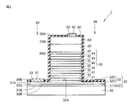
図1を参照して、実施の形態1における半導体積層体10は、基板20と、バッファ層30と、受光層40と、ブロック層50と、コンタクト層60とを備えている。
(Embodiment 1)
Referring to FIG. 1 , semiconductor stacked
基板20は、III-V族化合物半導体であるInPからなる。また、基板20の直径は50mm以上であり、たとえば3インチである。InPからなる基板20を採用することにより、赤外光用の受光素子の製造に適した半導体積層体10を得ることが容易となる。具体的には、たとえば導電型がn型であるInP(n-InP)が、基板20を構成する化合物半導体として採用される。基板20に含まれるn型不純物としては、たとえばS(硫黄)などを採用することができる。基板20の直径は、半導体積層体10を用いた半導体装置(受光素子)の生産効率および歩留りの向上を目的として、80mm以上(たとえば4インチ)とすることができ、さらに105mm以上(たとえば5インチ)、さらに130mm以上(たとえば6インチ)とすることができる。
The
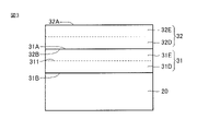
バッファ層30は、第一バッファ層31と、第一バッファ層31上に配置される第二バッファ層32と、を含む。第一バッファ層31は、基板20の一方の主面20A上に接触するように配置される半導体層である。第一バッファ層31は、III-V族化合物半導体であるInPからなる。具体的には、たとえば導電型がn型であるInP(n-InP)が、第一バッファ層31を構成する化合物半導体として採用される。第一バッファ層31に含まれるn型不純物としては、たとえばSi(珪素)などを採用することができる。本実施の形態における第一バッファ層31の厚みは、例えば、10nm以上50nm以下であり、より好ましくは10nm以上30nm以下であり、さらに好ましくは10nm以上20nm以下である。
The
第一バッファ層31は、1×1021cm-3未満のSbを含む。第一バッファ層31は、基板20よりもSbの濃度が高い第一の層31Dを含む。第一の層31Dは、基板20側の主面である第1主面31Bを含むように配置される。本実施の形態においては、第一バッファ層31全体が、第一の層31Dである。本実施の形態においては、第一の層31DのSbの濃度が、1×1016cm-3以上であり、より好ましくは1×1017cm-3以上である。第一の層31DのSbの濃度は、好ましくは1×1020cm-3以下である。
The
ここで、Sbの濃度は、SIMSを用いて測定した各層の厚み方向における濃度分布の積分値を各層の厚みで除した値である。例えば、SIMSを用いて、厚み方向におけるSbの濃度分布の測定を3か所において実施する。そして各箇所の各層におけるSbの濃度を算出して、その平均値を各層におけるSbの濃度とすることができる。なお、SIMSによる測定においては、基板20側から測定を行う方法(バックサイドSIMS)を用いてもよい。このような方法を用いて測定を行うことで、厚み方向におけるSbの濃度分布の測定をより精度良く行うことができる。
Here, the concentration of Sb is a value obtained by dividing the integrated value of the concentration distribution in the thickness direction of each layer measured using SIMS by the thickness of each layer. For example, SIMS is used to measure the concentration distribution of Sb in the thickness direction at three locations. Then, the Sb concentration in each layer at each location is calculated, and the average value thereof can be used as the Sb concentration in each layer. In addition, in the measurement by SIMS, a method of performing measurement from the
第二バッファ層32は、第一バッファ層31の、第1主面31B側とは反対側の主面31A上に接触するように配置される半導体層である。第二バッファ層32は、3元系のIII-V族化合物半導体であるInGaAsからなる。具体的には、たとえば導電型がn型であるInGaAs(n-InGaAs)が、第二バッファ層32を構成する化合物半導体として採用される。バッファ層30に含まれるn型不純物としては、たとえばSiを採用することができる。
The
第二バッファ層32は、第一の層31DよりもSbの濃度が低い第二の層32Dを含む。第二の層32Dは、第一バッファ層31側の主面である第2主面32Bを含むように配置される。第一バッファ層31に接する第二の層32D以外の領域には、第四の層32Eが配置されている。Sbの濃度が、1×1020cm-3以下である場合には、第二の層32Dが形成されているものと判断される。本実施の形態において、第二の層32DのSbの濃度は、好ましくは1×1017cm-3以下であり、より好ましくは1×1016cm-3以下である。本実施の形態における第二バッファ層32の厚みは、例えば、100nm以上200nm以下である。
The
受光層40は、第二バッファ層32の、第2主面32Bとは反対側の主面32A上に接触するように配置されている。受光層40は、III-V族化合物半導体からなる2つの要素層が交互に積層された量子井戸構造を有している。より具体的には、受光層40は、第1要素層41と第2要素層42とが交互に積層された構造を有している。本実施の形態における受光層40は、タイプII量子井戸構造である。第1要素層41を構成する材料としては、たとえばInxGa1-xAs(xは0.38以上1以下)を採用することができる。第1要素層41は、意図的にはSbが添加されない層(成長時に原料ガスに意図的にSbの原料ガスが添加されない層)である。また、第2要素層42を構成する材料としては、たとえばV族元素としてSbを含むGaAs1-ySby(yは0.36以上1以下)(ガリウム砒素アンチモン)を採用することができる。なお、第1要素層41および第2要素層42を構成する材料は、上記材料に限られず、たとえば第1要素層41を構成する材料としては、Ga1-uInuNvAs1-v(uは0.4以上0.8以下、vは0を超え0.2以下)(ガリウムインジウム窒素砒素)を採用し、第2要素層42を構成する材料としては、たとえばV族元素としてSbを含むGaAs1-ySby(yは0.36以上0.62以下)を採用することができる。
The
このように、受光層40としてInxGa1-xAs(xは0.38以上1以下)層とGaAs1-ySby(yは0.36以上1以下)層とのペア、またはGa1-uInuNvAs1-v(uは0.4以上0.8以下、vは0を超え0.2以下)層とGaAs1-ySby(yは0.36以上0.62以下)層とのペアを含む多重量子井戸構造を採用することにより、近赤外域から中赤外域の光の検知に適した受光素子の製造に使用可能な半導体積層体10を得ることができる。
In this way, a pair of an In x Ga 1-x As (x is 0.38 or more and 1 or less) layer and a GaAs 1-y Sb y (y is 0.36 or more and 1 or less) layer as the
第1要素層131および第2要素層132の厚みは、たとえばそれぞれ5nmとすることができる。そして、受光層40は、第1要素層131と第2要素層132とからなる単位構造が、たとえば250組積層されたものとすることができる。すなわち、受光層40の厚みは、たとえば2.5μmとすることができる。
The thicknesses of the first element layer 131 and the second element layer 132 can each be, for example, 5 nm. The light-receiving
また、第1要素層41を構成する材料としてInAsを採用し、第2要素層42を構成する材料としてGaSbを採用してもよい。このように受光層40としてInAs層とGaSb層とのペアを含む多重量子井戸構造を採用することにより、波長4~12μmの赤外線の検知に適した受光素子の製造に使用可能な半導体積層体10を得ることができる。
Alternatively, InAs may be employed as the material forming the
図1を参照して、ブロック層50は、受光層40の、第二バッファ層32に面する側とは反対側の主面40A上に接触するように配置されている。ブロック層50は、III-V族化合物半導体からなっている。
Referring to FIG. 1 ,
ブロック層50を構成するIII-V族化合物半導体としては、たとえばInGaAs(インジウムガリウム砒素)などを採用することができる。具体的には、たとえばアンドープのInGaAs(ud-InGaAs)が、ブロック層50を構成する化合物半導体として採用される。ブロック層50を配置することにより、コンタクト層60に含まれる不純物が受光層40へと拡散することを抑制することができる。
InGaAs (indium gallium arsenide), for example, can be used as the III-V group compound semiconductor forming the
図1を参照して、コンタクト層60は、ブロック層50の、受光層40に面する側とは反対側の主面50A上に接触するように配置されている。コンタクト層60は、III-V族化合物半導体からなっている。
Referring to FIG. 1 ,
コンタクト層60を構成するIII-V族化合物半導体としては、たとえばInP、InAs、GaSb、GaAs、InGaAs(インジウムガリウム砒素)などを採用することができる。具体的には、たとえば導電型がp型であるInP(p-InP)が、コンタクト層60を構成する化合物半導体として採用される。コンタクト層60に含まれるp型不純物としては、たとえばZnなどを採用することができる。
InP, InAs, GaSb, GaAs, InGaAs (indium gallium arsenide), or the like can be used as the III-V group compound semiconductor forming the
本実施の形態においては、InPからなる基板20上に、Sbを含むInPからなる第一バッファ層31を形成する。第一バッファ層31の形成に際しては、第1主面31Bを含むようにSbの濃度が高い第一の層31Dを形成する。基板20に接触する領域にSbを導入することにより、表面平坦性に優れた第一バッファ層31を形成することができる。
In this embodiment, the
そして、第一バッファ層31上にInGaAsからなる第二バッファ層32を形成する。第二バッファ層32の形成に際しては、第2主面32Bを含むように、上記第一の層31DよりもSbの濃度が低い第二の層32Dを形成する。InPからなる基板20上に直接形成するのではなく、第一バッファ層31上に第二バッファ層32を形成し、かつ第一バッファ層31に接触する領域において不要なSbの濃度を低減することにより、表面平坦性に優れた第二バッファ層32を形成することができる。このように、本実施の形態の半導体積層体10は、優れた表面平坦性を有するInGaAsからなる第二バッファ層32を備えた半導体積層体となっている。
Then, a
なお、上記実施の形態において、第一の層31DのSbの濃度は、1×1016cm-3以上である。第一の層31DのSbの濃度を上記範囲とすることで、第二バッファ層32の表面平坦性をより確実に優れたものとすることができる。第一の層31DのSbの濃度は、より好ましくは1×1017cm-3以上である。このようにすることで、第二バッファ層32の表面平坦性をさらに優れたものとすることができる。
In the above embodiment, the Sb concentration of the
上記実施の形態において、第二の層32DのSbの濃度は、1×1020cm-3以下である。第二の層32DのSbの濃度を上記範囲とすることで、第二バッファ層の表面平坦性をより確実に優れたものとすることができる。
In the above embodiment, the Sb concentration of the
上記実施の形態においては、第一バッファ層31の厚み方向におけるSbの濃度の分布において、Sbの濃度の最大値に対する最大値と最小値との差の割合が、50%以下である。上記割合を50%以下とすることで、表面平坦性が良好な第一バッファ層31を形成することができる。そのため、第二バッファ層32の表面平坦性をより確実に優れたものとすることができる。上記割合は、好ましくは20%以下であり、さらに好ましくは10%以下である。なお、上記割合が50%以下であるか否かの判断は、たとえば以下の通りである。SIMSを用いて、厚み方向におけるSbの濃度の線分析を、たとえば3か所において実施する。そして各箇所におけるSbの濃度の最大値に対する最大値と最小値との差の割合を算出し、その平均値が50%以下であれば、この条件を満たすものと判断することができる。
In the above embodiment, in the distribution of the Sb concentration in the thickness direction of the
上記実施の形態において、第一バッファ層31の厚みは、10nm以上50nm以下である。第一バッファ層31の厚みが10nm未満の場合、第二バッファ層32の表面平坦性が向上する効果が小さいおそれがある。一方、第一バッファ層31の厚みが50nmを超えると、第一バッファ層31の十分な表面平坦性を確保することが難しくなるおそれがある。したがって、第一バッファ層31の厚みを上記範囲とすることで、第二バッファ層32の表面平坦性をより確実に優れたものとすることができる。
In the above embodiment, the thickness of the
半導体積層体10において、バッファ層30、受光層40、ブロック層50およびコンタクト層60が再成長界面を形成することなく基板20上に積層されていることが好ましい。これにより、感度を一層向上させることができる。
In the
半導体積層体10において、バッファ層30と受光層40との界面、受光層40とブロック層50との界面、およびブロック層50とコンタクト層60との界面における、酸素の濃度、炭素の濃度および水素の濃度は、いずれも1×1017cm-3以下であることが好ましい。これにより、感度を一層向上させることができる。
In the semiconductor stacked
また、半導体積層体10において、バッファ層30、受光層40、ブロック層50およびコンタクト層60は有機金属気相成長法により形成されていることが好ましい。これにより、高品質な結晶からなる半導体積層体10を得ることが容易となる。
Moreover, in the
(変形例)
第一の層31Dは、第一バッファ層31全体に形成される他、厚み方向の一部分に形成されるようにしてもよい。図3は、本実施の形態における半導体積層体10の変形例を示す。図3を参照して、第一の層31Dが厚み方向の一部分に形成されている。第一バッファ層31において、第一の層31Dの、基板に面する側とは反対側の主面311上に接触するように、第一の層31DよりもSbの濃度が低い第三の層31Eが配置されている。上述のように第一バッファ層31の表面平坦性を向上させる観点から、基板20に接触する領域にSbの濃度が高い第一の層31Dを配置することが重要である。したがって、第一バッファ層31の全体が第一の層31Dであることは必ずしも必要ではなく、第一の層31Dを基板20に接触する部分に形成する構造を採用した場合でも、表面平坦性に優れた第一バッファ層31を形成することができる。
(Modification)
The
次に、上記半導体積層体10を用いて作製される受光素子の一例である赤外線受光素子(フォトダイオード)について説明する。図2を参照して、本実施の形態における赤外線受光素子1は、上記本実施の形態の半導体積層体10を用いて作製されたものであって、半導体積層体10と同様に積層された基板20と、バッファ層30と、受光層40と、ブロック層50と、コンタクト層60とを備えている。そして、赤外線受光素子1には、コンタクト層60、ブロック層50および受光層40を貫通し、バッファ層30に到達するトレンチ99が形成されている。すなわち、トレンチ99の側壁99Aにおいて、コンタクト層60、ブロック層50および受光層40が露出している。また、トレンチ99の底壁99Bは、第二バッファ層32内に位置している。つまり、トレンチ99の底壁99Bにおいて第二バッファ層32が露出している。
Next, an infrared light receiving element (photodiode), which is an example of a light receiving element manufactured using the
さらに、赤外線受光素子1は、パッシベーション膜80と、n側電極91と、p側電極92とを備えている。パッシベーション膜80はトレンチ99の底壁99B、トレンチ99の側壁99A、およびコンタクト層60の、ブロック層50に面する側とは反対側の主面60Aを覆うように配置されている。パッシベーション膜80は、窒化珪素、酸化珪素などの絶縁体からなっている。
Furthermore, the infrared
トレンチ99の底壁99Bを覆うパッシベーション膜80には、パッシベーション膜80を厚み方向に貫通するように開口部81が形成されている。そして、開口部81を充填するようにn側電極91が配置されている。n側電極91は、開口部81から露出する第二バッファ層32に接触するように配置されている。n側電極91は金属などの導電体からなっている。より具体的には、n側電極91は、たとえばTi(チタン)/Pt(白金)/Au(金)からなるものとすることができる。n側電極91は、バッファ層30に対してオーミック接触している。
An
コンタクト層60の主面60Aを覆うパッシベーション膜80には、パッシベーション膜80を厚み方向に貫通するように開口部82が形成されている。そして、開口部82を充填するようにp側電極92が配置されている。p側電極92は、開口部82から露出するコンタクト層60に接触するように配置されている。p側電極92は金属などの導電体からなっている。より具体的には、p側電極92は、たとえばTi/Pt/Auからなるものとすることができる。p側電極92は、コンタクト層60に対してオーミック接触している。
An
この赤外線受光素子1に赤外線が入射すると、受光層40内の量子準位間で赤外線が吸収され、電子と正孔とのペアが生成する。そして、生成した電子と正孔とが光電流信号として赤外線受光素子1から取り出されることにより、赤外線が検出される。
When infrared light is incident on the infrared
なお、上記p側電極92は画素電極である。そして、上記赤外線受光素子1は、図2に示すように画素電極であるp側電極92が1つだけ含まれるものであってもよいし、複数の画素電極(p側電極92)を含むものであってもよい。具体的には、赤外線受光素子1は、図2に示す構造を単位構造とし、当該単位構造が、図2において基板20の一方の主面20Aに沿う方向に複数繰り返される構造を有していてもよい。この場合、赤外線受光素子1は、画素に対応する複数のp側電極92を有する一方で、n側電極91については1つだけ配置される。このような構造については、後述の実施の形態2において説明する。
The p-
本実施の形態の赤外線受光素子1は、上記本実施の形態の半導体積層体10を含んでいる。そのため、受光層40の結晶性を優れたものとすることができる。その結果、赤外線受光素子1の暗電流を低減することができる。したがって、本実施の形態の赤外線受光素子1は、高感度な受光素子となっている。
The infrared
次に、図4~図10を参照して、本実施の形態における半導体積層体10および赤外線受光素子1の製造方法の概要について説明する。
Next, with reference to FIGS. 4 to 10, an outline of a method for manufacturing the
図4を参照して、本実施の形態における半導体積層体10および赤外線受光素子1の製造方法では、まず工程(S10)として基板準備工程が実施される。この工程(S10)では、図6を参照して、たとえば直径2インチ(50.8mm)のn-InPからなる基板20が準備される。より具体的には、InPからなるインゴットをスライスすることにより、InPからなる基板20が得られる。この基板20の表面が研磨された後、洗浄等のプロセスを経て主面20Aの平坦性および清浄性が確保された基板20が準備される。
Referring to FIG. 4, in the method of manufacturing semiconductor stacked
次に、工程(S20)としてエピ層形成工程が実施される。この工程(S20)では、工程(S10)において準備された基板20の主面20A上に、エピ層であるバッファ層30、受光層40、ブロック層50およびコンタクト層60が形成される。このエピ層の形成は、たとえば有機金属気相成長により実施することができる。有機金属気相成長によるエピ層の形成は、たとえば基板加熱用のヒータを備えた回転テーブル上に基板20を載置し、基板20をヒータにより加熱しつつ基板上に原料ガスを供給することにより実施することができる。工程(S20)は、図5を参照して、第一バッファ層形成工程(S21)、第二バッファ層形成工程(S22)、受光層形成工程(S23)、ブロック層形成工程(S24)およびコンタクト層形成工程(S25)を含む。
Next, an epitaxial layer forming step is performed as step (S20). In this step (S20), epilayers such as
工程(S20)においては、まず工程(S21)が実施される。具体的には、図6を参照して、まず基板20の主面20A上に接触するように、n-InPからなる第一バッファ層31が有機金属気相成長により形成される。n-InPからなる第一バッファ層31の形成では、Inの原料ガスとして、たとえばTMIn(トリメチルインジウム)などを用いることができ、Pの原料ガスとして、たとえばTBP(ターシャリーブチルホスフィン)を用いることができる。n型不純物としてSiを添加する場合、たとえばSiH4(シラン)、SiH3(CH3)(モノメチルシラン)、TeESi(テトラエチルシラン)を原料ガスに添加することができる。
In step (S20), step (S21) is first performed. Specifically, referring to FIG. 6, first, a
ここで、第一バッファ層31を形成する工程では、第1主面31Bを含むように基板20よりもSbの濃度が高い第一の層31Dが形成される。具体的には、第一の層31Dの形成に際し、1×1016cm-3以上1×1021cm-3未満の濃度となるようにSbが導入される。Sbの導入は、たとえばTMSb(トリメチルアンチモン)、TESb(トリエチルアンチモン)、TIPSb(トリイソプロピルアンチモン)、TDMASb(トリジメチルアミノアンチモン)、TTBSb(トリターシャリーブチルアンチモン)などを原料ガスに添加することにより実施することができる。
Here, in the step of forming the
次に、工程(S22)が実施される。具体的には、図6および図7を参照して、第一バッファ層31の、基板20に面する側とは反対側の主面31A上に接触するように、n-InGaAsからなる第二バッファ層32が形成される。第二バッファ層32の形成は、上記第一バッファ層31の形成に引き続いて有機金属気相成長により実施することができる。n-InGaAsからなるバッファ層30の形成では、Inの原料ガスとしてたとえばTMIn(トリメチルインジウム)、TEIn(トリエチルインジウム)などを用いることができ、Gaの原料ガスとしてたとえばTEGa(トリエチルガリウム)、TMGa(トリメチルガリウム)などを用いることができ、Asの原料ガスとしてたとえばAsH3(アルシン)、TBAs(ターシャリーブチルアルシン)、TMAs(トリメチル砒素)などを用いることができる。また、n型不純物としてSiを添加する場合、たとえばSiH4(シラン)、SiH3(CH3)(モノメチルシラン)、TeESi(テトラエチルシラン)を原料ガスに添加することができる。
Next, step (S22) is performed. Specifically, referring to FIGS. 6 and 7, the
第二バッファ層32を形成する工程では、第2主面32Bを含むように第一の層31DよりもSbの濃度が低い第二の層32Dが形成される。具体的には、第二の層32Dの形成に際しては、Sbの導入は実施されない。その結果、1×1020cm-3以下のSbの濃度である第二の層が形成される。
In the step of forming the
次に、工程(S23)が実施される。具体的には、図7および図8を参照して、第二バッファ層32の、第2主面32Bとは反対側の主面32A上に接触するように、たとえばIII-V族化合物半導体であるInxGa1-xAs(xは0.38以上1以下)からなる第1要素層41と、III-V族化合物半導体であるGaAs1-ySby(yは0.36以上1以下)からなる第2要素層42とが交互に積層して形成されることにより、受光層40が形成される。受光層40の形成は、上記第二バッファ層32の形成に引き続いて有機金属気相成長により実施することができる。すなわち、受光層40の形成は、第二バッファ層32の形成の際に用いた装置内に基板20を配置した状態で、原料ガスを変更することにより実施することができる。
Next, step (S23) is performed. Specifically, referring to FIGS. 7 and 8,
InxGa1-xAs(xは0.38以上1以下)からなる第1要素層41の形成では、Inの原料としてたとえばTMIn、TEInなどを用いることができ、Gaの原料としてたとえばTEGa、TMGaなどを用いることができ、Sbの原料としてたとえばTMSb、TESb、TIPSb、TDMASb、TTBSbなどを用いることができる。GaAs1-ySby(yは0.36以上1以下)からなる第2要素層42の形成では、Gaの原料としてたとえばTEGa、TMGaなどを用いることができ、Asの原料としてたとえばTBAs(ターシャリーブチルアルシン)、TMAs(トリメチル砒素)などを用いることができ、Sbの原料としてたとえばTMSb、TESb、TIPSb、TDMASb、TTBSbなどを用いることができる。第1要素層41および第2要素層42は、たとえばそれぞれ厚みを5nmとし、第1要素層41と第2要素層42とからなる単位構造が、たとえば250組積層するように形成することができる。これにより、タイプII量子井戸である受光層40を形成することができる。
In the formation of the
次に、工程(S24)が実施される。具体的には、図8および図1を参照して、受光層40の、第二バッファ層32に面する側とは反対側の主面40A上に接触するように、たとえばud-InGaAsからなるブロック層50が形成される。ブロック層50の形成は、上記受光層40の形成に引き続いて有機金属気相成長により実施することができる。すなわち、ブロック層50の形成は、受光層40の形成の際に用いた装置内に基板20を配置した状態で、原料ガスを変更することにより実施することができる。
Next, step (S24) is performed. Specifically, referring to FIGS. 8 and 1, light-receiving
次に、工程(S25)が実施される。具体的には、図1を参照して、ブロック層50の、受光層40に面する側とは反対側の主面50A上に接触するように、たとえばp-InPからなるコンタクト層60が形成される。コンタクト層60の形成は、上記ブロック層50の形成に引き続いて有機金属気相成長により実施することができる。すなわち、コンタクト層60の形成は、ブロック層50の形成の際に用いた装置内に基板20を配置した状態で、原料ガスを変更することにより実施することができる。p型不純物としてZnを添加する場合、たとえばDMZn(ジメチル亜鉛)、DEZn(ジエチル亜鉛)を原料ガスに添加することができる。
Next, step (S25) is performed. Specifically, referring to FIG. 1, a
以上の手順により、本実施の形態における半導体積層体10が完成する。上述のように、工程(S20)を有機金属気相成長により実施することにより、半導体積層体10の生産効率を向上させることができる。なお、工程(S20)は有機金属原料のみを用いた有機金属気相成長法(全有機金属気相成長法)に限られず、たとえばAsの原料にAsH3(アルシン)、Siの原料にSiH4(シラン)などの水素化物を用いた有機金属気相成長法で実施してもよいが、全有機金属気相成長法を採用することにより、高品質な結晶からなる半導体積層体10を得ることができる。また、有機金属気相成長以外の方法により実施することも可能であって、たとえばMBE(Molecular Beam Epitaxy)法を用いてもよい。
Through the above procedure, the
また、工程(S21)~(S25)は、上述のように、装置内に基板20を配置した状態で、原料ガスを変更することにより連続的に実施されることが好ましい。すなわち、工程(S21)~(S25)は、バッファ層30、受光層40、ブロック層50およびコンタクト層60が再成長界面を形成することなく積層されるように実施されることが好ましい。これにより、感度の向上に寄与する半導体積層体10を得ることができる。
Moreover, as described above, the steps (S21) to (S25) are preferably performed continuously by changing the source gas while the
次に、図4を参照して、工程(S30)としてトレンチ形成工程が実施される。この工程(S30)では、図1および図9を参照して、上記工程(S10)~(S20)において作製された半導体積層体10に、コンタクト層60、ブロック層50および受光層40を貫通し、バッファ層30に到達するトレンチ99が形成される。トレンチ99は、たとえばコンタクト層60の主面60A上にトレンチ99の形状に対応する開口を有するマスク層を形成した上で、エッチングを実施することにより形成することができる。
Next, referring to FIG. 4, a trench forming step is performed as step (S30). In this step (S30), referring to FIGS. 1 and 9, the
次に、工程(S40)としてパッシベーション膜形成工程が実施される。この工程(S40)では、図9および図10を参照して、工程(S30)においてトレンチ99が形成された半導体積層体10に対し、パッシベーション膜80が形成される。具体的には、たとえばCVD(Chemical Vapor Deposition)により酸化珪素、窒化珪素などの絶縁体からなるパッシベーション膜80が形成される。パッシベーション膜80は、トレンチ99の底壁99B、トレンチ99の側壁99A、およびコンタクト層60の、ブロック層50に面する側とは反対側の主面60Aを覆うように形成される。
Next, a passivation film forming step is performed as a step (S40). In this step (S40), referring to FIGS. 9 and 10,
次に、工程(S50)として電極形成工程が実施される。この工程(S50)では、図10および図2を参照して、工程(S40)においてパッシベーション膜80が形成された半導体積層体10に、n側電極91およびp側電極92が形成される。具体的には、たとえばn側電極91およびp側電極92を形成すべき領域に対応する位置に開口を有するマスクをパッシベーション膜80上に形成し、当該マスクを用いてパッシベーション膜80に開口部81,82を形成する。その後、たとえば蒸着法により適切な導電体からなるn側電極91およびp側電極92を形成する。以上の工程により、本実施の形態における赤外線受光素子1が完成する。その後、たとえばダイシングにより各素子に分離される。
Next, an electrode forming step is performed as a step (S50). In this step (S50), referring to FIGS. 10 and 2, n-
(実施の形態2)
次に、本発明にかかる半導体装置の他の実施の形態である実施の形態2における受光素子について説明する。図11および図2を参照して、実施の形態2の赤外線受光素子1は、図2に示す構造を単位構造とし、当該単位構造が、基板20の一方の主面20Aに沿う方向に複数繰り返される構造を有している。そして、赤外線受光素子1は、画素に対応する複数のp側電極92を有する。一方、n側電極91は1つだけ配置される。
(Embodiment 2)
Next, a light-receiving element in Embodiment 2, which is another embodiment of the semiconductor device according to the present invention, will be described. 11 and 2, infrared
より具体的には、図11を参照して、実施の形態2の赤外線受光素子1のn側電極91は、基板20に沿う方向における末端に位置するトレンチ99の底壁に形成されている。また、当該末端に位置するトレンチ99に隣接するコンタクト層60上のp側電極92は省略される。本実施の形態における赤外線センサ100は、このような構造を有する赤外線受光素子1と、赤外線受光素子1に電気的に接続された読み出し回路(Read-Out Integrated Circuit;ROIC)70とを含んでいる。読み出し回路70は、たとえばCMOS(Complementary Metal Oxide Semiconductor)回路である。
More specifically, referring to FIG. 11, n-
読み出し回路70の本体71に設けられた複数の読み出し電極(図示しない)と赤外線受光素子1において画素電極として機能する複数のp側電極92とが、一対一の関係となるようにバンプ73を介して電気的に接続されている。また、赤外線受光素子1には、n側電極91に接触し、n側電極91が位置するトレンチ99の底壁および側壁に沿って延在するとともに、コンタクト層60上にまで到達する配線75が形成される。そして、配線75と読み出し回路70の本体71に設けられた接地電極(図示しない)とがバンプ72を介して電気的に接続されている。このような構造を有することにより、赤外線受光素子1の画素ごとの受光情報が各p側電極92(画素電極)から読み出し回路70の読み出し電極へと出力され、当該受光情報が読み出し回路70において集約されて、たとえば二次元の画像を得ることができる。
A plurality of readout electrodes (not shown) provided on the
(実施の形態3)
次に、本願の受光素子の実施の形態3について説明する。実施の形態3の赤外線受光素子1は基本的には実施の形態2の赤外線受光素子1と同様の構造を有し、同様の効果を奏する。しかしながら、実施の形態3においては、赤外線受光素子1の画素に対応する単位構造がトレンチ99により分離される構造に代えて、不純物が拡散されていない領域により分離される構造が採用される点において、実施の形態2の場合とは異なっている。以下、実施の形態2の場合とは異なっている点について主に説明する。
(Embodiment 3)
Next, Embodiment 3 of the light receiving element of the present application will be described. The infrared
図12を参照して、本実施の形態におけるコンタクト層60は、アンドープのInP(ud-InP)からなる。厚み方向から平面的に見て、コンタクト層60には、不純物が拡散された拡散領域61が間隔をあけて複数形成されている。拡散領域61の導電型はp型である。拡散領域61は、厚み方向において、コンタクト層60の、ブロック層50に面する側とは反対側の主面60Aから、ブロック層50にまで至るように形成されている。拡散領域61に含まれる不純物としては、たとえばZnなどを採用することができる。
Referring to FIG. 12,
上記拡散領域61は、たとえば以下のように形成することができる。まず、実施の形態1の場合と同様の手順で半導体積層体10を作製する。このとき、上述のようにコンタクト層60はアンドープとされる。次に、基板20に沿う方向における末端に一対のトレンチ98が形成される。トレンチ98は、コンタクト層60、ブロック層および受光層40を貫通し、第二バッファ層32内に底壁98Bが位置するように形成される。次に、トレンチ98の側壁98A、およびコンタクト層60の、ブロック層50に面する側とは反対側の主面60Aを覆うようにマスク層83が形成される。マスク層83は、たとえば窒化珪素からなる。次に、マスク層83において、厚み方向に貫通するように複数の開口部84が間隔をあけて形成される。開口部84は、拡散領域61を形成すべき領域に対応して配置される。その後、マスク層83の開口部84から、Znなどの不純物が拡散される。その結果、コンタクト層60において、不純物が拡散された拡散領域61と、不純物が拡散されていない領域62とが形成される。不純物が拡散されていない領域62によって、赤外線受光素子1の画素に対応する隣り合う単位構造が分離される。
The
赤外線受光素子1は、パッシベーション膜85と、n側電極94と、p側電極93とを備えている。パッシベーション膜85がマスク層83の、コンタクト層60に面する側とは反対側の主面83A上に接触するように配置される。パッシベーション膜85には、開口部84に対応するように厚み方向に貫通する複数の開口部86が間隔をあけて形成されている。開口部84および開口部86を充填するようにp側電極93が配置されている。p側電極93は、開口部84から露出するコンタクト層60に接触するように配置されている。p側電極93は、たとえばAu(金)/Zn(亜鉛)からなるものとすることができる。
The infrared
n側電極94は、トレンチ98の底壁98Bにおいて第二バッファ層32と接触し、トレンチ98の側壁98Aおよびコンタクト層60の主面60Aを覆うように形成されたマスク層83上にまで延びるように配置されている。n側電極94は、たとえばAu(金)/Ge(ゲルマニウム)/Ni(ニッケル)からなるものとすることができる。
The n-
読み出し回路70における複数の読み出し電極(図示しない)と、赤外線受光素子1における複数のp側電極93とが、バンプ77を介して電気的に接続されている。そして、読み出し回路70における接地電極(図示しない)と、赤外線受光素子1におけるn側電極94とが、バンプ76を介して電気的に接続されている。
A plurality of readout electrodes (not shown) in the
上記実施の形態3の赤外線受光素子1によっても、実施の形態1と同様に、高感度な受光素子を得ることができる。
Also with the infrared
本願の半導体積層体の構造を確認する実験を行った。実験の手順は以下の通りである。 An experiment was conducted to confirm the structure of the semiconductor laminate of the present application. The experimental procedure is as follows.
まず、上記実施の形態1の場合と同様の手順で半導体積層体10を作製した。基板20としては、Sを不純物として含むInPを用いた。第一バッファ層31としては、Sbを原料ガスに導入しつつ、Siを不純物として含む厚み10nmのInP層を形成した。第二バッファ層32の形成の際には、Sbを原料ガスに導入せずに、Siを不純物として含む厚み150nmのInGaAs層を形成した。受光層40としては、厚み5nmのInGaAsからなる第1要素層41と厚み5nmのGaAsSbからなる第2要素層42とが交互に250組積層したものを採用した。ブロック層50としては、厚み1000nmのud-InGaAs層を形成した。コンタクト層60としては、不純物としてZnを含む厚み750nmのInP層を形成した。得られた半導体積層体10のうち、基板20、バッファ層30および受光層40のSbの濃度の分布を半導体積層体10の厚み方向において測定した。
First, the semiconductor laminated
半導体積層体10の厚み方向におけるSbの濃度分布を二重収束セクター磁場型SIMSにより測定した。測定装置には、CAMECA社製の測定装置を用いた。SIMSによる分析のためのスパッタリングには、セシウムイオン(Cs+)を用いた。セシウムイオンの加速電圧を15keVとした。ビーム径を20μm以下とした。ラスター領域を、一辺150μmの正方形領域とした。分析領域を、直径60μmの円形領域とした。測定時の真空度を、1×10-7Paとした。図13において、横軸は半導体積層体10の厚み方向の距離であり、縦軸はSbの濃度(cm-3)を示している。なお、Sbの濃度の測定限界(下限値)は、1×1016cm-3である。図13において、Sbの濃度が1×1016cm-3である場合、測定限界以下のSbの濃度を有するものと判断される。図13を参照して、領域S1は基板20に対応する。領域S2は第一バッファ層31に対応する。領域S3および領域S4は第二バッファ層32に対応する。領域S5は受光層40に対応する。領域S1と領域S2との境界では、Sbの濃度が急激に上昇する。領域S2においては、領域S1におけるSbの濃度よりも高い領域が形成されている。領域S2においては、Sbの濃度の高い第一の層31Dが形成されていることが確認される。なお、領域S2において、Sbの濃度の最大値と最小値との差の最大値に対する割合は、47%である。領域S2と領域S3との境界では、Sbの濃度が急激に減少する。領域S3は、第二の層32Dに対応する。領域S3と領域S4との境界では、Sbの濃度が急激に上昇する。このように領域S4においてSbの濃度が上昇するのは、受光層40からSbが拡散したためであると考えられる。このようにして第一の層31Dを含む第一バッファ層31を形成することにより、含まない場合に比べて、第一バッファ層31の表面平坦性が向上する。その結果、第二バッファ層32の表面平坦性が向上し、受光層40の結晶性が優れたものとなる。
The concentration distribution of Sb in the thickness direction of the
今回開示された実施の形態および実施例はすべての点で例示であって、どのような面からも制限的なものではないと理解されるべきである。本発明の範囲は上記した説明ではなく、特許請求の範囲によって規定され、特許請求の範囲と均等の意味および範囲内でのすべての変更が含まれることが意図される。 It should be understood that the embodiments and examples disclosed this time are illustrative in all respects and not restrictive in any aspect. The scope of the present invention is defined by the scope of the claims rather than the above description, and is intended to include all modifications within the meaning and range of equivalents of the scope of the claims.
本願の半導体積層体および受光素子は、感度の向上が求められる受光素子および当該受光素子の製造に用いられる半導体積層体に、特に有利に適用され得る。 The semiconductor laminate and the light-receiving element of the present application can be applied particularly advantageously to a light-receiving element that requires improved sensitivity and a semiconductor laminate used for manufacturing the light-receiving element.
1 赤外線受光素子
10 半導体積層体
20 基板
20A,31A,32A,40A,50A,60A,83A,311 主面
30 バッファ層
31 第一バッファ層
31B 第1主面
31D 第一の層
32D 第二の層
31E 第三の層
32E 第四の層
32 第二バッファ層
32B 第2主面
40 受光層
41,131 第1要素層
42,132 第2要素層
50 ブロック層
60 コンタクト層
61 拡散領域
62 領域
70 読み出し回路
71 本体
72,73,76,77 バンプ
75 配線
80,85 パッシベーション膜
81,82,84,86 開口部
83 マスク層
91,94 n側電極
92,93 p側電極
98,99 トレンチ
98A,99A 側壁
98B,99B 底壁
100 赤外線センサ
1 infrared
Claims (10)
前記基板上に配置され、1×1021cm-3未満のSbを含むInPからなる第一バッファ層と、
前記第一バッファ層上に配置され、InGaAsからなる第二バッファ層と、を備え、
前記第一バッファ層は、前記基板側の主面である第1主面を含むように配置され、前記基板よりもSbの濃度が高い第一の層を含み、
前記第二バッファ層は、前記第一バッファ層側の主面である第2主面を含むように配置され、前記第一の層よりもSbの濃度が低い第二の層を含む、半導体積層体。 a substrate made of InP;
a first buffer layer disposed on the substrate and made of InP containing less than 1×10 21 cm −3 of Sb;
a second buffer layer disposed on the first buffer layer and made of InGaAs;
The first buffer layer is arranged to include a first main surface that is the main surface on the substrate side, and includes a first layer having a higher Sb concentration than the substrate,
The second buffer layer is disposed so as to include a second main surface which is a main surface on the first buffer layer side, and includes a second layer having a lower Sb concentration than the first layer. body.
前記半導体積層体上に形成された電極と、を備える、受光素子。 A semiconductor laminate according to any one of claims 1 to 9;
and an electrode formed on the semiconductor laminate.
Priority Applications (2)
| Application Number | Priority Date | Filing Date | Title |
|---|---|---|---|
| JP2019004259A JP7147570B2 (en) | 2019-01-15 | 2019-01-15 | Semiconductor laminate and light receiving element |
| US16/676,942 US11152521B2 (en) | 2019-01-15 | 2019-11-07 | Semiconductor laminate and light-receiving element |
Applications Claiming Priority (1)
| Application Number | Priority Date | Filing Date | Title |
|---|---|---|---|
| JP2019004259A JP7147570B2 (en) | 2019-01-15 | 2019-01-15 | Semiconductor laminate and light receiving element |
Publications (2)
| Publication Number | Publication Date |
|---|---|
| JP2020113668A JP2020113668A (en) | 2020-07-27 |
| JP7147570B2 true JP7147570B2 (en) | 2022-10-05 |
Family
ID=71517776
Family Applications (1)
| Application Number | Title | Priority Date | Filing Date |
|---|---|---|---|
| JP2019004259A Active JP7147570B2 (en) | 2019-01-15 | 2019-01-15 | Semiconductor laminate and light receiving element |
Country Status (2)
| Country | Link |
|---|---|
| US (1) | US11152521B2 (en) |
| JP (1) | JP7147570B2 (en) |
Citations (4)
| Publication number | Priority date | Publication date | Assignee | Title |
|---|---|---|---|---|
| US20100258894A1 (en) | 2009-04-08 | 2010-10-14 | Sumitomo Electric Industries, Ltd. | Photodiode array and image pickup device using the same |
| JP2011060853A (en) | 2009-09-07 | 2011-03-24 | Sumitomo Electric Ind Ltd | Group iii-v compound semiconductor light receiving element and method of manufacturing the same |
| JP2011100770A (en) | 2009-11-04 | 2011-05-19 | Sumitomo Electric Ind Ltd | Method for manufacturing light receiving element array and light receiving element array, and method for manufacturing epitaxial wafer and epitaxial wafer |
| JP2015082573A (en) | 2013-10-22 | 2015-04-27 | 住友電気工業株式会社 | Epitaxial wafer and method of manufacturing the same |
Family Cites Families (3)
| Publication number | Priority date | Publication date | Assignee | Title |
|---|---|---|---|---|
| JPH08250752A (en) * | 1995-03-13 | 1996-09-27 | Advantest Corp | Photoconductor |
| JP2009027046A (en) * | 2007-07-21 | 2009-02-05 | Sumitomo Electric Ind Ltd | Light-receiving element |
| JP4662188B2 (en) | 2008-02-01 | 2011-03-30 | 住友電気工業株式会社 | Light receiving element, light receiving element array and manufacturing method thereof |
-
2019
- 2019-01-15 JP JP2019004259A patent/JP7147570B2/en active Active
- 2019-11-07 US US16/676,942 patent/US11152521B2/en active Active
Patent Citations (4)
| Publication number | Priority date | Publication date | Assignee | Title |
|---|---|---|---|---|
| US20100258894A1 (en) | 2009-04-08 | 2010-10-14 | Sumitomo Electric Industries, Ltd. | Photodiode array and image pickup device using the same |
| JP2011060853A (en) | 2009-09-07 | 2011-03-24 | Sumitomo Electric Ind Ltd | Group iii-v compound semiconductor light receiving element and method of manufacturing the same |
| JP2011100770A (en) | 2009-11-04 | 2011-05-19 | Sumitomo Electric Ind Ltd | Method for manufacturing light receiving element array and light receiving element array, and method for manufacturing epitaxial wafer and epitaxial wafer |
| JP2015082573A (en) | 2013-10-22 | 2015-04-27 | 住友電気工業株式会社 | Epitaxial wafer and method of manufacturing the same |
Also Published As
| Publication number | Publication date |
|---|---|
| US20200227576A1 (en) | 2020-07-16 |
| JP2020113668A (en) | 2020-07-27 |
| US11152521B2 (en) | 2021-10-19 |
Similar Documents
| Publication | Publication Date | Title |
|---|---|---|
| JP5975417B2 (en) | Manufacturing method of light receiving element | |
| JP2014127499A (en) | Light-receiving device, manufacturing method therefor, and sensing device | |
| JP2016092037A (en) | Semiconductor laminate, light receiving element and sensor | |
| JP2014236067A (en) | Semiconductor element and manufacturing method of the same | |
| US10790401B2 (en) | Semiconductor stacked body and light-receiving device | |
| WO2016171009A1 (en) | Semiconductor laminate, light-receiving element and method of manufacturing semiconductor laminate | |
| US10326034B2 (en) | Semiconductor laminate and light-receiving element | |
| JP6613923B2 (en) | Semiconductor laminate, light receiving element, and method of manufacturing semiconductor laminate | |
| JP6488855B2 (en) | Semiconductor laminate, light receiving element, and method of manufacturing semiconductor laminate | |
| US9929301B2 (en) | Semiconductor stack and semiconductor device | |
| JP6488854B2 (en) | Semiconductor laminate and light receiving element | |
| JP6454981B2 (en) | Semiconductor laminate and light receiving element | |
| US9887310B2 (en) | Semiconductor layered structure, method for producing semiconductor layered structure, and method for producing semiconductor device | |
| JP7147570B2 (en) | Semiconductor laminate and light receiving element | |
| WO2016067996A1 (en) | Semiconductor laminate, light receiving element and sensor | |
| JP6233070B2 (en) | Semiconductor stacked body, semiconductor device, and manufacturing method thereof | |
| US11081605B2 (en) | Semiconductor laminate, light-receiving element, and method for manufacturing semiconductor laminate | |
| WO2012073934A1 (en) | Light receiving element, semiconductor epitaxial wafer, method for manufacturing the light receiving element and the semiconductor epitaxial wafer, and detecting apparatus | |
| JP2016092036A (en) | Semiconductor laminate, light receiving element and sensor |
Legal Events
| Date | Code | Title | Description |
|---|---|---|---|
| A621 | Written request for application examination |
Free format text: JAPANESE INTERMEDIATE CODE: A621 Effective date: 20211021 |
|
| TRDD | Decision of grant or rejection written | ||
| A977 | Report on retrieval |
Free format text: JAPANESE INTERMEDIATE CODE: A971007 Effective date: 20220817 |
|
| A01 | Written decision to grant a patent or to grant a registration (utility model) |
Free format text: JAPANESE INTERMEDIATE CODE: A01 Effective date: 20220823 |
|
| A61 | First payment of annual fees (during grant procedure) |
Free format text: JAPANESE INTERMEDIATE CODE: A61 Effective date: 20220905 |
|
| R150 | Certificate of patent or registration of utility model |
Ref document number: 7147570 Country of ref document: JP Free format text: JAPANESE INTERMEDIATE CODE: R150 |