JP7136371B2 - power converter - Google Patents

power converter Download PDF

Info

Publication number
JP7136371B2
JP7136371B2 JP2021572170A JP2021572170A JP7136371B2 JP 7136371 B2 JP7136371 B2 JP 7136371B2 JP 2021572170 A JP2021572170 A JP 2021572170A JP 2021572170 A JP2021572170 A JP 2021572170A JP 7136371 B2 JP7136371 B2 JP 7136371B2
Authority
JP
Japan
Prior art keywords
capacitor
terminal
power converter
semiconductor module
coolers
Prior art date
Legal status (The legal status is an assumption and is not a legal conclusion. Google has not performed a legal analysis and makes no representation as to the accuracy of the status listed.)
Active
Application number
JP2021572170A
Other languages
Japanese (ja)
Other versions
JPWO2021149165A1 (en
JPWO2021149165A5 (en
Inventor
崇功 川島
直之 岸本
洋平 今井
Current Assignee (The listed assignees may be inaccurate. Google has not performed a legal analysis and makes no representation or warranty as to the accuracy of the list.)
Denso Corp
Original Assignee
Denso Corp
Priority date (The priority date is an assumption and is not a legal conclusion. Google has not performed a legal analysis and makes no representation as to the accuracy of the date listed.)
Filing date
Publication date
Application filed by Denso Corp filed Critical Denso Corp
Publication of JPWO2021149165A1 publication Critical patent/JPWO2021149165A1/ja
Publication of JPWO2021149165A5 publication Critical patent/JPWO2021149165A5/ja
Application granted granted Critical
Publication of JP7136371B2 publication Critical patent/JP7136371B2/en
Active legal-status Critical Current
Anticipated expiration legal-status Critical

Links

Images

Classifications

    • HELECTRICITY
    • H02GENERATION; CONVERSION OR DISTRIBUTION OF ELECTRIC POWER
    • H02MAPPARATUS FOR CONVERSION BETWEEN AC AND AC, BETWEEN AC AND DC, OR BETWEEN DC AND DC, AND FOR USE WITH MAINS OR SIMILAR POWER SUPPLY SYSTEMS; CONVERSION OF DC OR AC INPUT POWER INTO SURGE OUTPUT POWER; CONTROL OR REGULATION THEREOF
    • H02M7/00Conversion of ac power input into dc power output; Conversion of dc power input into ac power output
    • H02M7/42Conversion of dc power input into ac power output without possibility of reversal
    • H02M7/44Conversion of dc power input into ac power output without possibility of reversal by static converters
    • H02M7/48Conversion of dc power input into ac power output without possibility of reversal by static converters using discharge tubes with control electrode or semiconductor devices with control electrode

Description

本明細書が開示する技術は、電力変換用のスイッチング素子を収容する半導体モジュールが一対の冷却器に挟まれている電力変換器に関する。 The technology disclosed in this specification relates to a power converter in which a semiconductor module containing switching elements for power conversion is sandwiched between a pair of coolers.

一対の冷却器の間に半導体モジュールが挟まれており、半導体モジュールの内部のスイッチング素子が冷却器の隣りに配置されたコンデンサに接続されている電力変換器が知られている。特開2018-42424号公報(文献1)に、そのような電力変換器の例が開示されている。冷却器と半導体モジュールは第1方向に沿って並んでおり、半導体モジュールの第2方向を向く面から端子が延びている。一対の冷却器は第3方向の両側にて、連結パイプで連結されている。なお、第1方向、第2方向、第3方向は、互いに直交する方向を示す。コンデンサは第3方向で半導体モジュールに隣り合っている。 A power converter is known in which a semiconductor module is sandwiched between a pair of coolers, and a switching element inside the semiconductor module is connected to a capacitor arranged next to the cooler. Japanese Patent Laying-Open No. 2018-42424 (Document 1) discloses an example of such a power converter. The cooler and the semiconductor module are arranged along the first direction, and terminals extend from the surface of the semiconductor module facing the second direction. A pair of coolers are connected by connecting pipes on both sides in the third direction. Note that the first direction, the second direction, and the third direction indicate directions orthogonal to each other. The capacitor is adjacent to the semiconductor module in the third direction.

電力変換器では、スイッチング素子からコンデンサまでの電流経路で発生するインダクタンスが電力損失の一因となる。文献1の電力変換器の構造では、コンデンサと半導体モジュールの間には連結パイプが位置する。それゆえ、スイッチング素子(半導体モジュール)からコンデンサまでの電流経路が長くなり、大きいインダクタンスが発生する。 In a power converter, the inductance generated in the current path from the switching element to the capacitor is one of the causes of power loss. In the power converter structure of Document 1, a connecting pipe is positioned between the capacitor and the semiconductor module. Therefore, the current path from the switching element (semiconductor module) to the capacitor becomes long, resulting in large inductance.

本明細書が開示する電力変換器では、半導体モジュールの第2方向を向く第1面に対向するようにコンデンサを配置する。先に述べたように、第2方向を向く第1面に端子が設けられている。端子が設けられている第1面に対向するようにコンデンサ素子を配置することで、半導体モジュールの端子からコンデンサまでの距離が短くなる。すなわち半導体モジュールの中のスイッチング素子からコンデンサまでの電流経路が短くなり、インダクタンスを抑えることができる。 In the power converter disclosed in this specification, the capacitor is arranged to face the first surface facing the second direction of the semiconductor module. As previously mentioned, the terminals are provided on the first surface facing the second direction. By arranging the capacitor element so as to face the first surface on which the terminals are provided, the distance from the terminals of the semiconductor module to the capacitor is shortened. That is, the current path from the switching element in the semiconductor module to the capacitor is shortened, and the inductance can be suppressed.

本明細書が開示する電力変換器の一態様では、コンデンサは、第3方向における両端に電極を備える。半導体モジュールの正極端子は、コンデンサの側面に沿って第3方向に延びており、先端がコンデンサの一方の電極に接続される。半導体モジュールの負極端子は、正極端子とは逆方向に延びており、先端がコンデンサの他方の電極に接続される。この態様によると、コンデンサの中を流れる電流の方向が正極端子(負極端子)を流れる電流の方向と逆になる。互いに逆方向に電流が流れると電流経路で発生するインダクタンスを相殺することができる。すなわち、インダクタンスのさらなる低減が期待できる。 In one aspect of the power converter disclosed in this specification, the capacitor includes electrodes at both ends in the third direction. The positive terminal of the semiconductor module extends in the third direction along the side surface of the capacitor, and its tip is connected to one electrode of the capacitor. The negative terminal of the semiconductor module extends in the opposite direction to the positive terminal, and its tip is connected to the other electrode of the capacitor. According to this aspect, the direction of current flowing through the capacitor is opposite to the direction of current flowing through the positive terminal (negative terminal). When currents flow in directions opposite to each other, the inductance generated in the current paths can be canceled. That is, further reduction in inductance can be expected.

本明細書が開示する技術の詳細とさらなる改良は以下の「発明を実施するための形態」にて説明する。 Details and further improvements of the technique disclosed in this specification are described in the following "Mode for Carrying Out the Invention".

電力変換器の回路図である。It is a circuit diagram of a power converter. 半導体モジュールの斜視図である。1 is a perspective view of a semiconductor module; FIG. 図2のIII-III線に沿った半導体モジュールの断面図である。3 is a cross-sectional view of the semiconductor module taken along line III-III in FIG. 2; FIG. 第1実施例の電力変換器の斜視図である。1 is a perspective view of a power converter of a first embodiment; FIG. 第1実施例の電力変換器の斜視図である(コンデンサを外した状態)。It is a perspective view of the power converter of 1st Example (state which removed the capacitor|condenser). 電力変換器の正面図である。It is a front view of a power converter. 第1変形例の電力変換器の平面図である。It is a top view of the power converter of a 1st modification. 第2実施例の電力変換器の斜視図である。It is a perspective view of the power converter of 2nd Example. 第2実施例の電力変換器の分解斜視図である。FIG. 7 is an exploded perspective view of the power converter of the second embodiment; 第2変形例の電力変換器の断面図である。It is a sectional view of the power converter of the 2nd modification.

(第1実施例)図1-図6を参照して第1実施例の電力変換器2を説明する。まず、電力変換器2の回路構成を説明する。図1に、電力変換器2の回路を示す。電力変換器2は、電気自動車90に搭載されている。電力変換器2はインバータであり、バッテリ91の直流電力を走行用のモータ92を駆動するための交流電力に変換する。 (First Embodiment) A power converter 2 of a first embodiment will be described with reference to FIGS. 1 to 6. FIG. First, the circuit configuration of the power converter 2 will be described. The circuit of the power converter 2 is shown in FIG. Power converter 2 is mounted on electric vehicle 90 . The power converter 2 is an inverter, and converts the DC power of the battery 91 into AC power for driving the motor 92 for running.

電力変換器2は、直流端の正極9aと負極9bの間に接続されているコンデンサ3と、電力変換用の6個のスイッチング素子4(4a、4b)と、6個のダイオード5(5a、5b)で構成される。6個のスイッチング素子4は、2個ずつ直列に接続される。正極9aの側のスイッチング素子4をスイッチング素子4aと称し、負極9bの側のスイッチング素子4をスイッチング素子4bと称する場合がある。 The power converter 2 includes a capacitor 3 connected between a positive electrode 9a and a negative electrode 9b at the DC end, six switching elements 4 (4a, 4b) for power conversion, and six diodes 5 (5a, 4b) for power conversion. 5b). The six switching elements 4 are connected in series two by two. The switching element 4 on the side of the positive electrode 9a may be called the switching element 4a, and the switching element 4 on the side of the negative electrode 9b may be called the switching element 4b.

3セットの直列接続回路(2個のスイッチング素子4a、4bの直列接続回路)が直流端の正極9aと負極9bの間に並列に接続される。それぞれのスイッチング素子4にダイオード5(5a、5b)が逆並列に接続される。スイッチング素子4aに並列に接続されるダイオード5をダイオード5aと称し、スイッチング素子4bに並列に接続されるダイオード5をダイオード5bと称する場合がある。2個のスイッチング素子4a、4bの直列接続回路の中点から交流が出力される。 Three sets of series-connected circuits (series-connected circuits of two switching elements 4a and 4b) are connected in parallel between the positive electrode 9a and the negative electrode 9b of the DC end. A diode 5 (5a, 5b) is connected in anti-parallel to each switching element 4. FIG. The diode 5 connected in parallel with the switching element 4a may be called a diode 5a, and the diode 5 connected in parallel with the switching element 4b may be called a diode 5b. Alternating current is output from the middle point of the series connection circuit of the two switching elements 4a and 4b.

6個のスイッチング素子4は、モータコントローラ6によって制御される。図1における矢印破線は信号線を示しており、モータコントローラ6からスイッチング素子4のゲートに信号線がつながっている。 Six switching elements 4 are controlled by a motor controller 6 . A dashed arrow line in FIG. 1 indicates a signal line, and the signal line is connected from the motor controller 6 to the gate of the switching element 4 .

モータコントローラ6は、上位のコントローラ94からモータ92の目標出力を受信すると、目標出力が実現するように6個のスイッチング素子4を制御する。正極側のスイッチング素子4aと負極側のスイッチング素子4bを交互にオンオフすると、直列接続回路の中点から交流が出力される。 When the motor controller 6 receives a target output of the motor 92 from the host controller 94, the motor controller 6 controls the six switching elements 4 so as to achieve the target output. When the switching element 4a on the positive electrode side and the switching element 4b on the negative electrode side are alternately turned on and off, alternating current is output from the midpoint of the series connection circuit.

直列に接続される2個のスイッチング素子4a、4bは半導体モジュール10に収容されている。符号10が示す破線矩形が半導体モジュールを示している。それぞれのスイッチング素子4a、4bに並列に接続されるダイオード5a、5bも半導体モジュール10に収容される。電力変換器2は、3個の半導体モジュール10(10a-10c)を備えている。3個の半導体モジュールを総称する場合は符号10を用い、それぞれの半導体モジュールを個別に表す場合には符号10a、10b、10cを用いる。半導体モジュール10のハードウエアの構造は後で説明する。 Two switching elements 4 a and 4 b connected in series are housed in a semiconductor module 10 . A dashed rectangle indicated by reference numeral 10 indicates a semiconductor module. Diodes 5a and 5b connected in parallel to the respective switching elements 4a and 4b are also housed in the semiconductor module 10 . The power converter 2 includes three semiconductor modules 10 (10a-10c). Reference numeral 10 is used to collectively refer to the three semiconductor modules, and reference numerals 10a, 10b, and 10c are used to refer to the respective semiconductor modules individually. The hardware structure of the semiconductor module 10 will be explained later.

半導体モジュール10は3個のパワー端子(正極端子11、負極端子12、中点端子13)を備えている。正極端子11、負極端子12、中点端子13は、それぞれ、2個のスイッチング素子4a、4bの直列接続回路の高電位側、低電位側、中点と接続される。 The semiconductor module 10 has three power terminals (a positive terminal 11, a negative terminal 12, and a midpoint terminal 13). The positive terminal 11, the negative terminal 12, and the midpoint terminal 13 are connected to the high potential side, the low potential side, and the midpoint, respectively, of the series connection circuit of the two switching elements 4a and 4b.

図2に、半導体モジュール10の斜視図を示す。図3に、図2のIII-III線に沿った断面を示す。半導体モジュール10の本体は樹脂製のパッケージ20であり、パッケージ20に2個の半導体チップ21a、21bが埋設されている。半導体チップ21aには図1のスイッチング素子4aとダイオード5aの並列回路が実装されており、半導体チップ21bには図1のスイッチング素子4bとダイオード5bの並列回路が実装されている。 FIG. 2 shows a perspective view of the semiconductor module 10. As shown in FIG. FIG. 3 shows a cross section along line III--III in FIG. The main body of the semiconductor module 10 is a package 20 made of resin, in which two semiconductor chips 21a and 21b are embedded. A parallel circuit of the switching element 4a and the diode 5a of FIG. 1 is mounted on the semiconductor chip 21a, and a parallel circuit of the switching element 4b and the diode 5b of FIG. 1 is mounted on the semiconductor chip 21b.

図3を参照してパッケージ20の内部の構造を説明する。半導体チップ21a、21bは扁平な板であり、その幅広面の両面に電極が露出している。半導体チップ21aの正極(スイッチング素子4aの正極)にはスペーサ24aが接合されており、スペーサ24aの反対側に金属板23aが接合されている。半導体チップ21aの負極(スイッチング素子4aの負極)は金属板22に接合されており、その金属板22には半導体チップ21bの正極(スイッチング素子4bの正極)が接合されている。すなわち、金属板22が2個のスイッチング素子4a、4bを直列に接続する。 The internal structure of the package 20 will be described with reference to FIG. The semiconductor chips 21a and 21b are flat plates, and electrodes are exposed on both sides of their wide surfaces. A spacer 24a is joined to the positive electrode of the semiconductor chip 21a (the positive electrode of the switching element 4a), and a metal plate 23a is joined to the opposite side of the spacer 24a. The negative electrode of the semiconductor chip 21a (negative electrode of the switching element 4a) is joined to the metal plate 22, and the positive electrode of the semiconductor chip 21b (positive electrode of the switching element 4b) is joined to the metal plate 22. That is, the metal plate 22 connects the two switching elements 4a and 4b in series.

半導体チップ21bの負極(スイッチング素子4bの負極)はスペーサ24bに接合されており、スペーサ24bの反対側に金属板23bが接合されている。金属板23aが2個のスイッチング素子4a、4bの直列接続回路の高電位側に対応し、金属板23bが直列接続回路の低電位側に対応する。 The negative electrode of the semiconductor chip 21b (the negative electrode of the switching element 4b) is joined to the spacer 24b, and the metal plate 23b is joined to the opposite side of the spacer 24b. The metal plate 23a corresponds to the high potential side of the series connection circuit of the two switching elements 4a and 4b, and the metal plate 23b corresponds to the low potential side of the series connection circuit.

金属板22、23a、23bの一方の面はパッケージ20から露出しており、半導体チップ21a、21bの熱を放出する。 One surface of the metal plates 22, 23a, 23b is exposed from the package 20 and radiates heat from the semiconductor chips 21a, 21b.

図2に戻り、半導体モジュール10の構造を説明する。パッケージ20は、扁平であり、図中の座標系の+Y方向を向く幅狭の面20aに正極端子11と負極端子12が設けられている。負極端子12は、第1幅狭面20aからY方向に延びている基部12aと、基部12aからX方向に直角に折れ曲がっている中間部12bと、中間部12bからY方向に直角に折れ曲がっている先端部12cを有する。正極端子11も同様であり、基部11a、中間部11b、先端部11cを有する。正極端子11の基部11aは、中間部11bに隠れて見えない。基部11a(12a)、中間部11b(12b)、先端部11c(12c)は、それぞれ平板である。 Returning to FIG. 2, the structure of the semiconductor module 10 will be described. The package 20 is flat, and the positive terminal 11 and the negative terminal 12 are provided on a narrow surface 20a facing the +Y direction of the coordinate system in the figure. The negative electrode terminal 12 has a base portion 12a extending in the Y direction from the first narrow surface 20a, an intermediate portion 12b bent at right angles to the X direction from the base portion 12a, and bent at right angles to the Y direction from the intermediate portion 12b. It has a tip portion 12c. Similarly, the positive electrode terminal 11 has a base portion 11a, an intermediate portion 11b, and a tip portion 11c. The base portion 11a of the positive electrode terminal 11 is hidden by the intermediate portion 11b and cannot be seen. The base portion 11a (12a), the intermediate portion 11b (12b), and the tip portion 11c (12c) are flat plates.

反対側のーY方向を向く幅狭の面20bに中点端子13と制御端子14a、14bが設けられている。説明の都合上、パッケージ20の+Y方向を向く面20aを以下では第1幅狭面20aと称し、-Y方向を向く面20bを第2幅狭面20bと称する。 A middle point terminal 13 and control terminals 14a and 14b are provided on the narrow surface 20b facing the -Y direction on the opposite side. For convenience of explanation, the surface 20a facing the +Y direction of the package 20 is hereinafter referred to as the first narrow surface 20a, and the surface 20b facing the -Y direction is referred to as the second narrow surface 20b.

正極端子11、負極端子12は、それぞれ、パッケージ20の内部で金属板23a、23bに接続されている。中点端子13は、パッケージ20の内部で金属板22に接続されている。正極端子11、負極端子12、中点端子13は、金属板22、23a、23bを介して2個の半導体チップ21a、21b(2個のスイッチング素子4a、4b)の直列接続回路の高電位側、低電位側、中点と導通する。別言すれば、正極端子11は、スイッチング素子4aの正極に接続され、負極端子12はスイッチング素子4bの負極に接続される。 The positive terminal 11 and the negative terminal 12 are connected to metal plates 23a and 23b inside the package 20, respectively. The midpoint terminal 13 is connected to the metal plate 22 inside the package 20 . The positive terminal 11, the negative terminal 12, and the midpoint terminal 13 are connected to the high potential side of a series connection circuit of two semiconductor chips 21a and 21b (two switching elements 4a and 4b) via metal plates 22, 23a and 23b. , the low potential side, and the middle point. In other words, the positive terminal 11 is connected to the positive terminal of the switching element 4a, and the negative terminal 12 is connected to the negative terminal of the switching element 4b.

制御端子14a(14b)は、半導体チップ21a(21b)の制御パッド(不図示)に接続されている。制御パッドは、スイッチング素子のゲート、温度センサ(不図示)の端子などで構成される。制御端子14a(14b)を介してモータコントローラ6からスイッチング素子4a(4b)へ駆動信号が送られる。 The control terminal 14a (14b) is connected to a control pad (not shown) of the semiconductor chip 21a (21b). The control pad is composed of a gate of a switching element, a terminal of a temperature sensor (not shown), and the like. A drive signal is sent from the motor controller 6 to the switching element 4a (4b) via the control terminal 14a (14b).

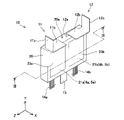
図4に、電力変換器2の斜視図を示す。図4は、電力変換器2の主要部品である半導体モジュール10とコンデンサ3のアセンブリの斜視図である。図4では、アセンブリ以外の部品(筐体を含む)の図示は省略してある。図5に、コンデンサ3を半導体モジュール10から外した状態の電力変換器2の斜視図を示す。 FIG. 4 shows a perspective view of the power converter 2. As shown in FIG. FIG. 4 is a perspective view of an assembly of a semiconductor module 10 and a capacitor 3, which are main components of the power converter 2. As shown in FIG. In FIG. 4, illustration of parts (including the housing) other than the assembly is omitted. FIG. 5 shows a perspective view of the power converter 2 with the capacitor 3 removed from the semiconductor module 10. As shown in FIG.

電力変換器2は、3個の半導体モジュール10(10a-10c)と、4個の冷却器30(30a-30d)と、コンデンサ3を備える。4個の冷却器30を総称する場合には符号30を用い、個別に表す場合には符号30a-30dを用いる。 The power converter 2 includes three semiconductor modules 10 (10a-10c), four coolers 30 (30a-30d), and a capacitor 3. Reference numeral 30 is used to refer to the four coolers 30 collectively, and reference numerals 30a to 30d are used to refer to them individually.

3個の半導体モジュール10と4個の冷却器30は、1個ずつ交互に積層される。複数の半導体モジュール10と複数の冷却器30は、図中の座標系のX方向に並んでいる。それぞれの半導体モジュール10は、一対の冷却器に挟まれることになる。例えば半導体モジュール10aは一対の冷却器30a、30bに挟まれる。半導体モジュール10bは一対の冷却器30b、30cに挟まれる。半導体モジュール10cは一対の冷却器30c、30dに挟まれる。 Three semiconductor modules 10 and four coolers 30 are alternately stacked one by one. A plurality of semiconductor modules 10 and a plurality of coolers 30 are arranged in the X direction of the coordinate system in the drawing. Each semiconductor module 10 is sandwiched between a pair of coolers. For example, the semiconductor module 10a is sandwiched between a pair of coolers 30a and 30b. The semiconductor module 10b is sandwiched between a pair of coolers 30b and 30c. The semiconductor module 10c is sandwiched between a pair of coolers 30c and 30d.

冷却器30の内部を冷媒が通る。冷媒は液体である。隣り合う冷却器30は、一対の連結パイプ31a、31bで連結される。連結パイプ31a、31bは、隣り合う冷却器30の中の流路をつなぐ。図の右端の冷却器30dには、冷媒入口32aと冷媒出口32bが設けられている。冷媒入口32aと冷媒出口32bは不図示の冷媒循環装置に接続される。冷媒入口32aから供給された冷媒は、連結パイプ31aを通じて全ての冷却器30に分配される。冷媒は冷却器30の内部を通過する間に隣り合う半導体モジュール10から熱を吸収する。熱を吸収した冷媒は連結パイプ31bを通じて冷媒出口32bから排出される。それぞれの半導体モジュール10は両面から冷却されるので、電力変換器2は半導体モジュール10に対する冷却効率が高い。 A refrigerant passes through the inside of the cooler 30 . The refrigerant is liquid. Adjacent coolers 30 are connected by a pair of connecting pipes 31a and 31b. The connecting pipes 31a and 31b connect flow paths in the coolers 30 adjacent to each other. A coolant inlet 32a and a coolant outlet 32b are provided in the cooler 30d on the right end of the figure. The refrigerant inlet 32a and the refrigerant outlet 32b are connected to a refrigerant circulation device (not shown). A refrigerant supplied from the refrigerant inlet 32a is distributed to all the coolers 30 through the connecting pipes 31a. The coolant absorbs heat from adjacent semiconductor modules 10 while passing through cooler 30 . The refrigerant that has absorbed heat is discharged from the refrigerant outlet 32b through the connecting pipe 31b. Since each semiconductor module 10 is cooled from both sides, the power converter 2 has a high cooling efficiency with respect to the semiconductor module 10 .

それぞれの半導体モジュール10の第1幅狭面20aに正極端子11と負極端子12が設けられている。先に述べたように、第1幅狭面20aは図中の座標系のY方向を向く面であり、正極端子11と負極端子12はZ方向に並んでいる。コンデンサ3は、半導体モジュール10の第1幅狭面20aに対向するように配置される。コンデンサ3は、図中の座標系のZ方向の両端に電極(正極3p、負極3n)を有している。 A positive terminal 11 and a negative terminal 12 are provided on the first narrow surface 20 a of each semiconductor module 10 . As described above, the first narrow surface 20a faces the Y direction of the coordinate system in the drawing, and the positive terminal 11 and the negative terminal 12 are aligned in the Z direction. Capacitor 3 is arranged to face first narrow surface 20 a of semiconductor module 10 . The capacitor 3 has electrodes (positive electrode 3p, negative electrode 3n) at both ends in the Z direction of the coordinate system in the figure.

半導体モジュール10の正極端子11の先端部11cと負極端子12の先端部12cは、Z方向でコンデンサ3を挟み込み、先端部11cがコンデンサ3の正極3pに接合され、先端部12cがコンデンサ3の負極3nに接合される。 The tip portion 11c of the positive terminal 11 and the tip portion 12c of the negative terminal 12 of the semiconductor module 10 sandwich the capacitor 3 in the Z direction, the tip portion 11c is joined to the positive electrode 3p of the capacitor 3, and the tip portion 12c is the negative electrode of the capacitor 3. 3n.

複数の半導体モジュール10の下方に回路基板7が配置される。回路基板7には図1に示したモータコントローラ6が実装されている。 A circuit board 7 is arranged below the plurality of semiconductor modules 10 . The motor controller 6 shown in FIG. 1 is mounted on the circuit board 7 .

図6に電力変換器2の正面図を示す。半導体モジュール10の第2幅狭面20bに制御端子14a、14bと中点端子13が設けられている。回路基板7は、第2幅狭面20bに対向するように配置される。制御端子14a、14bは、回路基板7に接続される。中点端子13は、回路基板7を通過し、別のバスバと接合される。バスバとは、金属棒(金属板)で作られた導電部材である。 FIG. 6 shows a front view of the power converter 2. As shown in FIG. Control terminals 14 a and 14 b and a midpoint terminal 13 are provided on the second narrow surface 20 b of the semiconductor module 10 . The circuit board 7 is arranged so as to face the second narrow surface 20b. The control terminals 14 a and 14 b are connected to the circuit board 7 . The midpoint terminal 13 passes through the circuit board 7 and is joined to another bus bar. A busbar is a conductive member made of a metal rod (metal plate).

先に述べたように、コンデンサ3は、半導体モジュール10の第1幅狭面20aに対向するように配置される。第1幅狭面20aには正極端子11と負極端子12が設けられている。図4-図6に示されているように、正極端子11(負極端子12)からコンデンサ3までの距離が短い。半導体モジュール10の内部のスイッチング素子4a、4bからコンデンサ3までの電流経路が短いので、電流経路で発生するインダクタンスを抑えることができる。電流経路で発生するインダクタンスは電力損失の原因となる。スイッチング素子からコンデンサまでの電流経路が短い電力変換器2は、損失が小さい。 As described above, the capacitor 3 is arranged to face the first narrow surface 20a of the semiconductor module 10 . A positive electrode terminal 11 and a negative electrode terminal 12 are provided on the first narrow surface 20a. As shown in FIGS. 4 to 6, the distance from the positive terminal 11 (negative terminal 12) to the capacitor 3 is short. Since the current path from the switching elements 4a and 4b inside the semiconductor module 10 to the capacitor 3 is short, the inductance generated in the current path can be suppressed. Inductance generated in the current path causes power loss. A power converter 2 having a short current path from a switching element to a capacitor has a small loss.

Z方向で半導体モジュール10の両側には連結パイプ31a、31bが配置されている。それゆえ、仮にZ方向で半導体モジュール10に隣り合うようにコンデンサ3を配置すると、半導体モジュール10内のスイッチング素子からコンデンサ3までの距離が長くなる。複数の半導体モジュール10と複数の冷却器30がX方向に並んでいる。従って、仮にX方向で半導体モジュール10に隣り合うようにコンデンサ3を配置した場合も、半導体モジュール10内のスイッチング素子からコンデンサ3までの距離が長くなる。実施例の電力変換器2では、Y方向で半導体モジュール10に隣り合うようにコンデンサ3が配置される。そのような配置が、半導体モジュール10内のスイッチング素子からコンデンサ3までの距離を最も短くすることができる。 Connection pipes 31a and 31b are arranged on both sides of the semiconductor module 10 in the Z direction. Therefore, if the capacitor 3 is arranged adjacent to the semiconductor module 10 in the Z direction, the distance from the switching element in the semiconductor module 10 to the capacitor 3 becomes long. A plurality of semiconductor modules 10 and a plurality of coolers 30 are arranged in the X direction. Therefore, even if the capacitor 3 is arranged adjacent to the semiconductor module 10 in the X direction, the distance from the switching element in the semiconductor module 10 to the capacitor 3 is long. In the power converter 2 of the embodiment, the capacitor 3 is arranged so as to be adjacent to the semiconductor module 10 in the Y direction. Such an arrangement can minimize the distance from the switching elements in the semiconductor module 10 to the capacitor 3 .

また、正極端子11の中間部11bと負極端子12の中間部12bは、コンデンサ3の側面に沿って延びており、Z軸に沿って互いに逆方向に延びている。正極端子11の先端部11cと負極端子12の先端部12cは互いに対向するように折れ曲がっており、それらの間にコンデンサ3が挟まれている。先に述べたように、正極端子11の先端部11cはコンデンサ3の正極3pに接合され、負極端子12の先端部12cはコンデンサ3の負極3nに接合される。 An intermediate portion 11b of the positive electrode terminal 11 and an intermediate portion 12b of the negative electrode terminal 12 extend along the side surface of the capacitor 3 and extend in opposite directions along the Z axis. The tip portion 11c of the positive electrode terminal 11 and the tip portion 12c of the negative electrode terminal 12 are bent so as to face each other, and the capacitor 3 is sandwiched between them. As described above, the tip portion 11c of the positive terminal 11 is joined to the positive electrode 3p of the capacitor 3, and the tip portion 12c of the negative electrode terminal 12 is joined to the negative electrode 3n of the capacitor 3. FIG.

図6に示されているように、コンデンサ3は、Z方向(正極端子11と負極端子12の並び方向)の中心線CLが正極端子11と負極端子12の間を通るように配置される。そして、正極端子11と負極端子12がコンデンサ3の側面に沿って互いに逆方向に延びている。この構成により、図6の太い矢印線が示すように電流が流れる。特に高周波のノイズはコンデンサ3の表層に沿って流れる。すなわち、正極端子11と負極端子12に流れる電流と、コンデンサ3の内部を流れる電流は、近接することになる。 As shown in FIG. 6 , the capacitor 3 is arranged such that the center line CL in the Z direction (direction in which the positive terminal 11 and the negative terminal 12 are arranged) passes between the positive terminal 11 and the negative terminal 12 . A positive terminal 11 and a negative terminal 12 extend in opposite directions along side surfaces of the capacitor 3 . This configuration causes current to flow as indicated by the thick arrow lines in FIG. In particular, high-frequency noise flows along the surface of capacitor 3 . That is, the current flowing through the positive terminal 11 and the negative terminal 12 and the current flowing inside the capacitor 3 are close to each other.

正極端子11の中間部11bと負極端子12の中間部12bでは電流は図中の右から左へ流れる。コンデンサ3の内部では、電流は左から右へと流れる。正極端子11と負極端子12を流れる電流とコンデンサ3の内部を流れる電流が互いに反対方向になるから、それぞれの電流が発生する磁界が相殺される。電流が発生する磁界が相殺されると電流変化に起因するインダクタンスが抑制される。電力変換器2では、磁界を相殺することでもインダクタンスが抑制され、その結果、損失が抑えられる。 Current flows from the right to the left in the figure between the intermediate portion 11b of the positive electrode terminal 11 and the intermediate portion 12b of the negative electrode terminal 12 . Inside the capacitor 3, the current flows from left to right. Since the current flowing through the positive terminal 11 and the negative terminal 12 and the current flowing inside the capacitor 3 are opposite to each other, the magnetic fields generated by the respective currents cancel each other out. When the magnetic field generated by the current is canceled, the inductance caused by the current change is suppressed. In the power converter 2, the inductance is also suppressed by canceling out the magnetic field, and as a result, the loss is suppressed.

図7に、変形例の電力変換器102の正面図を示す。実施例の半導体モジュール10は、第1幅狭面20aに正極端子11と負極端子12が設けられており、反対側の第2幅狭面20bに中点端子13が設けられている。変形例の電力変換器102に用いられている半導体モジュール110は、パッケージ20の第1幅狭面20aに正極端子111と負極端子112と中点端子113が設けられている。正極端子111と負極端子112と中点端子113は、第1幅狭面20aにて、Z方向に並んでいる。第1幅狭面20aに中点端子113も設けられ、正極端子111と負極端子112の間が狭められている。それでも、正極端子111と負極端子112は、Z方向で並んでおり、それらの間にコンデンサ103が配置される。コンデンサ103は第1幅狭面20aに対向するように配置される。コンデンサ103は、Z方向におけるコンデンサ103の中心線CLが正極端子111と負極端子112の間を通るように配置される。 FIG. 7 shows a front view of the power converter 102 of the modification. In the semiconductor module 10 of the embodiment, the positive terminal 11 and the negative terminal 12 are provided on the first narrow surface 20a, and the midpoint terminal 13 is provided on the second narrow surface 20b on the opposite side. A semiconductor module 110 used in the power converter 102 of the modified example is provided with a positive terminal 111 , a negative terminal 112 and a midpoint terminal 113 on the first narrow surface 20 a of the package 20 . The positive terminal 111, the negative terminal 112, and the midpoint terminal 113 are arranged in the Z direction on the first narrow surface 20a. A midpoint terminal 113 is also provided on the first narrow surface 20a to narrow the space between the positive terminal 111 and the negative terminal 112 . Nevertheless, the positive terminal 111 and the negative terminal 112 are aligned in the Z direction, with the capacitor 103 placed between them. The capacitor 103 is arranged to face the first narrow surface 20a. The capacitor 103 is arranged such that the center line CL of the capacitor 103 in the Z direction passes between the positive terminal 111 and the negative terminal 112 .

正極端子111と負極端子112は、コンデンサ103の側面に沿って互いに反対方向へ延びており、正極端子111はコンデンサ103の正極3pに接合しており、負極端子112は負極3nと接合している。変形例の電力変換器102も実施例の電力変換器2と同じ効果を奏する。 The positive terminal 111 and the negative terminal 112 extend in opposite directions along the side surface of the capacitor 103, the positive terminal 111 is connected to the positive electrode 3p of the capacitor 103, and the negative terminal 112 is connected to the negative electrode 3n. . The power converter 102 of the modification also has the same effects as the power converter 2 of the embodiment.

(第2実施例)図8、図9を用いて第2実施例の電力変換器202を説明する。図8は、電力変換器202の斜視図であり、図9は電力変換器202の分解斜視図である。第2実施例の電力変換器202は、第1実施例の電力変換器2が用いた半導体モジュール10(10a-10c)を用いるが、その並べ方が第1実施例の場合と異なる。 (Second Embodiment) A power converter 202 of a second embodiment will be described with reference to FIGS. 8 and 9. FIG. 8 is a perspective view of power converter 202, and FIG. 9 is an exploded perspective view of power converter 202. FIG. The power converter 202 of the second embodiment uses the semiconductor modules 10 (10a-10c) used in the power converter 2 of the first embodiment, but the arrangement is different from that of the first embodiment.

電力変換器202では、一対の冷却器230a、230bの間に、3個の半導体モジュール10a-10cが挟まれている。3個の半導体モジュール10a-10cは、図中の座標系のZ方向に並んでいる。Z方向は、半導体モジュール10において正極端子11と負極端子12の並び方向と同じである。 In power converter 202, three semiconductor modules 10a-10c are sandwiched between a pair of coolers 230a and 230b. The three semiconductor modules 10a-10c are arranged in the Z direction of the coordinate system in the drawing. The Z direction is the same as the direction in which the positive terminal 11 and the negative terminal 12 are arranged in the semiconductor module 10 .

第1実施例の電力変換器2では、3個の半導体モジュール10a-10cのそれぞれの正極端子11と負極端子12が1個のコンデンサ3に接続されている。第2実施例の電力変換器202は、3個のコンデンサ3a-3cを有しており、半導体モジュール10a-10cのそれぞれが3個のコンデンサ3a-3cのそれぞれに接続されている。 In the power converter 2 of the first embodiment, the positive terminal 11 and the negative terminal 12 of each of the three semiconductor modules 10a-10c are connected to one capacitor 3. As shown in FIG. The power converter 202 of the second embodiment has three capacitors 3a-3c, and each of the semiconductor modules 10a-10c is connected to each of the three capacitors 3a-3c.

電力変換器202は、3個の半導体モジュール10a-10cの並び方が相違するだけで、他の特徴は電力変換器2の特徴と同じである。それゆえ、第2実施例の電力変換器2も第1実施例の電力変換器2と同じ利点を有する。 The power converter 202 has the same features as the power converter 2 except for the arrangement of the three semiconductor modules 10a to 10c. Therefore, the power converter 2 of the second embodiment also has the same advantages as the power converter 2 of the first embodiment.

(変形例)図10に変形例の電力変換器302の側面図を示す。図10では、冷却器330a、330bと半導体モジュール310とコンデンサ3を収容する筐体380も描いてある。図10は、電力変換器302の筐体380を図中の座標系のXY平面でカットした断面を示している。一対の冷却器330a、330bと半導体モジュール310とコンデンサ3は側面が描かれている。 (Modification) FIG. 10 shows a side view of a power converter 302 of a modification. FIG. 10 also depicts a housing 380 that accommodates the coolers 330a and 330b, the semiconductor module 310, and the capacitor 3. FIG. FIG. 10 shows a cross section of housing 380 of power converter 302 taken along the XY plane of the coordinate system in the drawing. A pair of coolers 330a and 330b, the semiconductor module 310, and the capacitor 3 are depicted in side view.

変形例の電力変換器302では、半導体モジュール310の端子の形状が半導体モジュール10とは若干相違する。電力変換器302も一対の冷却器330aと330bの間に3個の半導体モジュール310が挟まれている。3個の半導体モジュール310はZ方向に並んでおり、2個の半導体モジュール310は、図10の紙面奥側に配置されている。 In the power converter 302 of the modified example, the terminal shape of the semiconductor module 310 is slightly different from that of the semiconductor module 10 . Power converter 302 also has three semiconductor modules 310 sandwiched between a pair of coolers 330a and 330b. The three semiconductor modules 310 are arranged in the Z direction, and the two semiconductor modules 310 are arranged on the back side of the paper surface of FIG.

一対の冷却器330a、330bと半導体モジュール310は図中座標系のX方向に並んでおり、それぞれの半導体モジュール310の正極端子311と負極端子(図10では負極端子は正極端子311に隠れて見えない)はZ方向で並んでおり、コンデンサ3はY方向で半導体モジュール310の第1幅狭面20aに対向している、正極端子311と負極端子(図1では不図示)は、Z方向でコンデンサ3を挟んでいる。これらの構造は、第2実施例の電力変換器202と同じである。それゆえ、変形例の電力変換器302は、第2実施例の電力変換器202と同じ利点を有する。 The pair of coolers 330a and 330b and the semiconductor module 310 are arranged in the X direction of the coordinate system in the figure, and the positive terminal 311 and the negative terminal of each semiconductor module 310 (the negative terminal is hidden behind the positive terminal 311 in FIG. 10). ) are arranged in the Z direction, the capacitor 3 faces the first narrow surface 20a of the semiconductor module 310 in the Y direction, and the positive terminal 311 and the negative terminal (not shown in FIG. 1) are arranged in the Z direction. It sandwiches the capacitor 3. These structures are the same as the power converter 202 of the second embodiment. Therefore, the modified power converter 302 has the same advantages as the power converter 202 of the second embodiment.

モータコントローラ6が実装された回路基板307は、冷却器330a、330bと半導体モジュール310のアセンブリの上方に配置されている。回路基板307は筐体380に固定されている。半導体モジュール310の制御端子314は上方に折れ曲がっており、回路基板307に接続されている。中点端子313は中間バスバ384の一端に連結されている。中間バスバ384の他端は出力バスバ385の一端に連結されている。出力バスバ385は、筐体380の外へと延びている。出力バスバ385は、走行用のモータ92(図1参照)に接続される。 A circuit board 307 on which the motor controller 6 is mounted is arranged above the assembly of the coolers 330 a and 330 b and the semiconductor module 310 . Circuit board 307 is fixed to housing 380 . A control terminal 314 of the semiconductor module 310 is bent upward and connected to the circuit board 307 . The center point terminal 313 is connected to one end of the intermediate bus bar 384 . The other end of the intermediate busbar 384 is connected to one end of the output busbar 385 . The output busbar 385 extends outside the housing 380 . The output busbar 385 is connected to the driving motor 92 (see FIG. 1).

回路基板307は、伝熱シート382を挟んで冷却器330aと対向している。図10では理解を助けるため、伝熱シート382をグレーで示してある。回路基板307は、冷却器330aと熱的に接続されている。図10において回路基板7から冷却器330aに向かう矢印線は熱の流れを表している。図10の構造によると、回路基板7は冷却器330aにより冷却される。 The circuit board 307 faces the cooler 330a with the heat transfer sheet 382 interposed therebetween. In FIG. 10, the heat transfer sheet 382 is shown in gray to aid understanding. The circuit board 307 is thermally connected to the cooler 330a. In FIG. 10, arrow lines from the circuit board 7 to the cooler 330a represent heat flow. According to the structure of FIG. 10, the circuit board 7 is cooled by the cooler 330a.

コンデンサ3の下面は筐体380の底板381に接している。また、冷却器330bも底板381に接している。コンデンサ3の下部から底板381に向かう矢印線、および、底板381から冷却器330bへ向かう矢印線も熱の流れを示している。それらの矢印線が示すように、コンデンサ3は冷却器330bにより冷却される。 The bottom surface of the capacitor 3 is in contact with the bottom plate 381 of the housing 380 . Cooler 330 b is also in contact with bottom plate 381 . An arrow line from the bottom of the capacitor 3 to the bottom plate 381 and an arrow line from the bottom plate 381 to the cooler 330b also indicate heat flow. As indicated by those arrow lines, condenser 3 is cooled by cooler 330b.

実施例で説明した電力変換器2(102、202、303)の特徴を以下に列挙する。コンデンサ3は、正極端子11と負極端子12が設けられている第1幅狭面と対向するように配置されている。コンデンサは、Z方向における中心線CLが正極端子11と負極端子12の間を通るように配置されている。コンデンサ3は、Z方向における両端に電極(正極3pと負極3n)を備える。正極端子11は、コンデンサ3の側面に沿ってZ方向に延びており、先端部11cがコンデンサ3の一方の電極(例えば正極3p)に接続される。負極端子12はコンデンサ3の側面に沿って正極端子11とは逆方向に延びており、先端部12cがコンデンサ3の他方の電極(例えば負極3n)に接続される。上記の構造により、半導体モジュール10の内部のスイッチング素子4a、4bからコンデンサ3までの電流経路が短くなり、電流経路に発生するインダクタンスを抑えることができる。また、正極端子11(負極端子12)とコンデンサ3の内部で電流が逆方向に流れる。この構造も、インダクタンスの抑制に貢献する。 The features of the power converter 2 (102, 202, 303) described in the embodiment are enumerated below. The capacitor 3 is arranged so as to face the first narrow surface on which the positive terminal 11 and the negative terminal 12 are provided. The capacitor is arranged such that the center line CL in the Z direction passes between the positive terminal 11 and the negative terminal 12 . The capacitor 3 has electrodes (a positive electrode 3p and a negative electrode 3n) at both ends in the Z direction. The positive electrode terminal 11 extends in the Z direction along the side surface of the capacitor 3, and the tip portion 11c is connected to one electrode of the capacitor 3 (for example, the positive electrode 3p). The negative electrode terminal 12 extends along the side surface of the capacitor 3 in the direction opposite to the positive electrode terminal 11, and the tip portion 12c is connected to the other electrode of the capacitor 3 (for example, the negative electrode 3n). With the above structure, the current path from the switching elements 4a and 4b inside the semiconductor module 10 to the capacitor 3 is shortened, and the inductance generated in the current path can be suppressed. In addition, the current flows in the positive terminal 11 (negative terminal 12) and the inside of the capacitor 3 in opposite directions. This structure also contributes to suppression of inductance.

半導体モジュール10には2個のスイッチング素子4a、4bの直列接続回路が収容されている。正極端子11は直列接続回路の高電位側に接続されており、負極端子12は直列接続回路の低電位側に接続されている。直列接続回路の中点に接続されている中点端子13は、第1幅狭面の反対側の第2幅狭面から延びている。 A semiconductor module 10 accommodates a series connection circuit of two switching elements 4a and 4b. The positive terminal 11 is connected to the high potential side of the series connection circuit, and the negative terminal 12 is connected to the low potential side of the series connection circuit. A midpoint terminal 13 connected to the midpoint of the series circuit extends from the second narrow face opposite the first narrow face.

複数の冷却器30がX方向に並んでおり、複数の半導体モジュール10と複数の冷却器30がX方向に沿って1個ずつ交互に積層されている。それぞれの半導体モジュール10の正極端子11と負極端子12がコンデンサ3に接続される。 A plurality of coolers 30 are arranged in the X direction, and a plurality of semiconductor modules 10 and a plurality of coolers 30 are alternately stacked along the X direction. A positive terminal 11 and a negative terminal 12 of each semiconductor module 10 are connected to the capacitor 3 .

第2実施例の電力変換器202では、複数の半導体モジュール10がZ方向に沿って並んでいる。一対の冷却器230a、230bが複数の半導体モジュール10a-10cを挟んでいる。 In the power converter 202 of the second embodiment, multiple semiconductor modules 10 are arranged along the Z direction. A pair of coolers 230a, 230b sandwich the plurality of semiconductor modules 10a-10c.

実施例で説明した技術に関する留意点を述べる。図のX方向、Y方向、Z方向がそれぞれ、第1方向、第2方向、第3方向に対応する。第1幅狭面20aが、正極端子11と負極端子12が設けられている第1面に対応する。実施例の半導体モジュールでは第1幅狭面20aと第2幅狭面20bはともに平坦であったが、第1幅狭面20aと第2幅狭面20bは平坦でなくともよい。 Points to note regarding the technology described in the embodiment will be described. The X direction, Y direction, and Z direction in the drawing correspond to the first direction, the second direction, and the third direction, respectively. The first narrow surface 20a corresponds to the first surface on which the positive terminal 11 and the negative terminal 12 are provided. In the semiconductor module of the embodiment, both the first narrow surface 20a and the second narrow surface 20b are flat, but the first narrow surface 20a and the second narrow surface 20b may not be flat.

本明細書が開示する技術は少なくとも1個の半導体モジュールが一対の冷却器に挟まれている電力変換器に適用することができる。本明細書が開示する技術は半導体モジュールの数、冷却器の数に限定されない。 The technology disclosed in this specification can be applied to a power converter in which at least one semiconductor module is sandwiched between a pair of coolers. The technology disclosed in this specification is not limited to the number of semiconductor modules and the number of coolers.

以上、本発明の具体例を詳細に説明したが、これらは例示に過ぎず、請求の範囲を限定するものではない。請求の範囲に記載の技術には、以上に例示した具体例を様々に変形、変更したものが含まれる。本明細書または図面に説明した技術要素は、単独であるいは各種の組合せによって技術的有用性を発揮するものであり、出願時請求項記載の組合せに限定されるものではない。また、本明細書または図面に例示した技術は複数目的を同時に達成し得るものであり、そのうちの一つの目的を達成すること自体で技術的有用性を持つものである。 Although specific examples of the present invention have been described in detail above, these are merely examples and do not limit the scope of the claims. The technology described in the claims includes various modifications and changes of the specific examples illustrated above. The technical elements described in this specification or in the drawings exhibit technical usefulness alone or in various combinations, and are not limited to the combinations described in the claims as of the filing. In addition, the techniques exemplified in this specification or drawings can simultaneously achieve a plurality of purposes, and achieving one of them has technical utility in itself.

Claims (5)

電力変換用のスイッチング素子を収容している半導体モジュールと、
前記半導体モジュールの第1面に設けられており、前記スイッチング素子と導通している正極端子と負極端子と、
前記半導体モジュールを挟み込んでいる一対の冷却器と、
前記スイッチング素子と電気的に接続されているコンデンサと、
を備えており、
前記半導体モジュールと一対の前記冷却器が第1方向で並んでおり、
前記第1面は、第1方向に交差する第2方向を向いており、
前記正極端子と前記負極端子は前記第1方向と前記第2方向の両方と交差する第3方向で並んでおり、
前記コンデンサは、前記第1面に対向するように配置されているとともに、前記第3方向における両端に電極を備えており、
前記正極端子は、前記コンデンサの側面に沿って前記第3方向に延びており、先端が前記コンデンサの一方の前記電極に接続されており、
前記負極端子は、前記側面に沿って前記正極端子とは逆方向に延びており、先端が前記コンデンサの他方の前記電極に接続されている、電力変換器。
a semiconductor module housing a switching element for power conversion;
a positive terminal and a negative terminal provided on the first surface of the semiconductor module and electrically connected to the switching element;
a pair of coolers sandwiching the semiconductor module;
a capacitor electrically connected to the switching element;
and
The semiconductor module and the pair of coolers are arranged in a first direction,
The first surface faces a second direction that intersects with the first direction,
the positive terminal and the negative terminal are arranged in a third direction crossing both the first direction and the second direction;
The capacitor is arranged to face the first surface and has electrodes at both ends in the third direction,
the positive electrode terminal extends in the third direction along the side surface of the capacitor and has a tip end connected to one of the electrodes of the capacitor;
The power converter , wherein the negative terminal extends in a direction opposite to the positive terminal along the side surface and has a tip end connected to the other electrode of the capacitor .
前記コンデンサは、前記第3方向における中心線が前記正極端子と前記負極端子の間を通るように配置されている、請求項1に記載の電力変換器。 2. The power converter according to claim 1 , wherein said capacitor is arranged such that a center line in said third direction passes between said positive terminal and said negative terminal. 前記半導体モジュールには2個の前記スイッチング素子の直列接続回路が収容されており、
前記正極端子は前記直列接続回路の高電位側に接続されており、
前記負極端子は前記直列接続回路の低電位側に接続されており、
前記直列接続回路の中点に接続されている中点端子が前記第1面の反対側の第2面から延びている、請求項1または2に記載の電力変換器。
The semiconductor module contains a series connection circuit of two switching elements,
the positive terminal is connected to the high potential side of the series connection circuit,
the negative terminal is connected to the low potential side of the series connection circuit,
3. A power converter according to claim 1 or 2 , wherein a midpoint terminal connected to the midpoint of said series circuit extends from a second surface opposite said first surface.
一対の前記冷却器を含む複数の前記冷却器が前記第1方向に並んでおり、
前記半導体モジュールを含む複数の前記半導体モジュールと複数の前記冷却器が前記第1方向に沿って1個ずつ交互に積層されており、それぞれの前記半導体モジュールの前記正極端子と前記負極端子が前記コンデンサに接続されている、請求項1からのいずれか1項に記載の電力変換器。
A plurality of the coolers including a pair of the coolers are arranged in the first direction,
A plurality of the semiconductor modules including the semiconductor modules and a plurality of the coolers are alternately stacked one by one along the first direction, and the positive terminal and the negative terminal of each of the semiconductor modules are connected to the capacitor. 4. A power converter as claimed in any one of claims 1 to 3 , connected to a
前記半導体モジュールを含む複数の前記半導体モジュールが前記第3方向に沿って並んでおり、
一対の前記冷却器が複数の前記半導体モジュールを挟んでいる、請求項1からのいずれか1項に記載の電力変換器。
a plurality of the semiconductor modules including the semiconductor module are arranged along the third direction;
4. The power converter according to any one of claims 1 to 3 , wherein a pair of said coolers sandwich a plurality of said semiconductor modules.
JP2021572170A 2020-01-21 2020-01-21 power converter Active JP7136371B2 (en)

Applications Claiming Priority (1)

Application Number Priority Date Filing Date Title
PCT/JP2020/001996 WO2021149165A1 (en) 2020-01-21 2020-01-21 Power converter

Publications (3)

Publication Number Publication Date
JPWO2021149165A1 JPWO2021149165A1 (en) 2021-07-29
JPWO2021149165A5 JPWO2021149165A5 (en) 2022-03-16
JP7136371B2 true JP7136371B2 (en) 2022-09-13

Family

ID=76993183

Family Applications (1)

Application Number Title Priority Date Filing Date
JP2021572170A Active JP7136371B2 (en) 2020-01-21 2020-01-21 power converter

Country Status (2)

Country Link
JP (1) JP7136371B2 (en)
WO (1) WO2021149165A1 (en)

Citations (6)

* Cited by examiner, † Cited by third party
Publication number Priority date Publication date Assignee Title
JP2011114966A (en) 2009-11-27 2011-06-09 Denso Corp Power conversion apparatus
US20110242725A1 (en) 2008-10-08 2011-10-06 Mtu Aero Engines Gmbh Capacitor arrangement and method for producing a capacitor arrangement
JP2011259544A (en) 2010-06-07 2011-12-22 Denso Corp Power conversion apparatus
JP2017163756A (en) 2016-03-10 2017-09-14 株式会社デンソー Power conversion device
JP2019097237A (en) 2017-11-20 2019-06-20 株式会社デンソー Electric power conversion system
WO2019244502A1 (en) 2018-06-19 2019-12-26 株式会社デンソー Electric power converter

Patent Citations (6)

* Cited by examiner, † Cited by third party
Publication number Priority date Publication date Assignee Title
US20110242725A1 (en) 2008-10-08 2011-10-06 Mtu Aero Engines Gmbh Capacitor arrangement and method for producing a capacitor arrangement
JP2011114966A (en) 2009-11-27 2011-06-09 Denso Corp Power conversion apparatus
JP2011259544A (en) 2010-06-07 2011-12-22 Denso Corp Power conversion apparatus
JP2017163756A (en) 2016-03-10 2017-09-14 株式会社デンソー Power conversion device
JP2019097237A (en) 2017-11-20 2019-06-20 株式会社デンソー Electric power conversion system
WO2019244502A1 (en) 2018-06-19 2019-12-26 株式会社デンソー Electric power converter

Also Published As

Publication number Publication date
WO2021149165A1 (en) 2021-07-29
JPWO2021149165A1 (en) 2021-07-29

Similar Documents

Publication Publication Date Title
US8686601B2 (en) Power conversion apparatus for vehicle use
US6822850B2 (en) Laminated bus bar for use with a power conversion configuration
US6885553B2 (en) Bus bar assembly for use with a compact power conversion assembly
JP2014090629A (en) Power conversion device
JP7151599B2 (en) power converter
JP6969502B2 (en) Power converter
JP7035845B2 (en) Power converter
JP2015139270A (en) Power conversion device
US6956742B2 (en) Compact liquid converter assembly
CN111541380A (en) Integrated mechanical and thermal design of power storage device of traction inverter
JP2013090408A (en) Electric power conversion device
JP7136371B2 (en) power converter
US11916491B2 (en) Electric power converter
JP6943212B2 (en) Power converter
JP7136139B2 (en) power converter
JP6699494B2 (en) Semiconductor laminated unit
JP7035543B2 (en) Power converter
JP6372433B2 (en) Power converter
JP7078182B2 (en) Power converters and electric vehicles
US20220304198A1 (en) Power converter
JP2019140722A (en) Power conversion device
WO2021014512A1 (en) Power converter
JP2021111709A (en) Power conversion apparatus
US20200343828A1 (en) Inverter using power module
JP2020137134A (en) Power converter

Legal Events

Date Code Title Description
A521 Request for written amendment filed

Free format text: JAPANESE INTERMEDIATE CODE: A523

Effective date: 20211220

A621 Written request for application examination

Free format text: JAPANESE INTERMEDIATE CODE: A621

Effective date: 20211220

TRDD Decision of grant or rejection written
A01 Written decision to grant a patent or to grant a registration (utility model)

Free format text: JAPANESE INTERMEDIATE CODE: A01

Effective date: 20220802

A61 First payment of annual fees (during grant procedure)

Free format text: JAPANESE INTERMEDIATE CODE: A61

Effective date: 20220815

R151 Written notification of patent or utility model registration

Ref document number: 7136371

Country of ref document: JP

Free format text: JAPANESE INTERMEDIATE CODE: R151