JP7086562B2 - Bandgap reference circuit - Google Patents
Bandgap reference circuit Download PDFInfo
- Publication number
- JP7086562B2 JP7086562B2 JP2017211132A JP2017211132A JP7086562B2 JP 7086562 B2 JP7086562 B2 JP 7086562B2 JP 2017211132 A JP2017211132 A JP 2017211132A JP 2017211132 A JP2017211132 A JP 2017211132A JP 7086562 B2 JP7086562 B2 JP 7086562B2
- Authority
- JP
- Japan
- Prior art keywords
- current
- node
- resistance element
- variable resistance
- bandgap reference
- Prior art date
- Legal status (The legal status is an assumption and is not a legal conclusion. Google has not performed a legal analysis and makes no representation as to the accuracy of the status listed.)
- Active
Links
Images


Classifications
-
- G—PHYSICS
- G05—CONTROLLING; REGULATING
- G05F—SYSTEMS FOR REGULATING ELECTRIC OR MAGNETIC VARIABLES
- G05F3/00—Non-retroactive systems for regulating electric variables by using an uncontrolled element, or an uncontrolled combination of elements, such element or such combination having self-regulating properties
- G05F3/02—Regulating voltage or current
- G05F3/08—Regulating voltage or current wherein the variable is dc
- G05F3/10—Regulating voltage or current wherein the variable is dc using uncontrolled devices with non-linear characteristics
- G05F3/16—Regulating voltage or current wherein the variable is dc using uncontrolled devices with non-linear characteristics being semiconductor devices
- G05F3/20—Regulating voltage or current wherein the variable is dc using uncontrolled devices with non-linear characteristics being semiconductor devices using diode- transistor combinations
- G05F3/26—Current mirrors
- G05F3/267—Current mirrors using both bipolar and field-effect technology
-
- G—PHYSICS
- G05—CONTROLLING; REGULATING
- G05F—SYSTEMS FOR REGULATING ELECTRIC OR MAGNETIC VARIABLES
- G05F3/00—Non-retroactive systems for regulating electric variables by using an uncontrolled element, or an uncontrolled combination of elements, such element or such combination having self-regulating properties
- G05F3/02—Regulating voltage or current
- G05F3/08—Regulating voltage or current wherein the variable is dc
- G05F3/10—Regulating voltage or current wherein the variable is dc using uncontrolled devices with non-linear characteristics
- G05F3/16—Regulating voltage or current wherein the variable is dc using uncontrolled devices with non-linear characteristics being semiconductor devices
- G05F3/20—Regulating voltage or current wherein the variable is dc using uncontrolled devices with non-linear characteristics being semiconductor devices using diode- transistor combinations
- G05F3/22—Regulating voltage or current wherein the variable is dc using uncontrolled devices with non-linear characteristics being semiconductor devices using diode- transistor combinations wherein the transistors are of the bipolar type only
- G05F3/222—Regulating voltage or current wherein the variable is dc using uncontrolled devices with non-linear characteristics being semiconductor devices using diode- transistor combinations wherein the transistors are of the bipolar type only with compensation for device parameters, e.g. Early effect, gain, manufacturing process, or external variations, e.g. temperature, loading, supply voltage
- G05F3/225—Regulating voltage or current wherein the variable is dc using uncontrolled devices with non-linear characteristics being semiconductor devices using diode- transistor combinations wherein the transistors are of the bipolar type only with compensation for device parameters, e.g. Early effect, gain, manufacturing process, or external variations, e.g. temperature, loading, supply voltage producing a current or voltage as a predetermined function of the temperature
-
- G—PHYSICS
- G05—CONTROLLING; REGULATING
- G05F—SYSTEMS FOR REGULATING ELECTRIC OR MAGNETIC VARIABLES
- G05F3/00—Non-retroactive systems for regulating electric variables by using an uncontrolled element, or an uncontrolled combination of elements, such element or such combination having self-regulating properties
- G05F3/02—Regulating voltage or current
- G05F3/08—Regulating voltage or current wherein the variable is dc
- G05F3/10—Regulating voltage or current wherein the variable is dc using uncontrolled devices with non-linear characteristics
- G05F3/16—Regulating voltage or current wherein the variable is dc using uncontrolled devices with non-linear characteristics being semiconductor devices
- G05F3/20—Regulating voltage or current wherein the variable is dc using uncontrolled devices with non-linear characteristics being semiconductor devices using diode- transistor combinations
- G05F3/24—Regulating voltage or current wherein the variable is dc using uncontrolled devices with non-linear characteristics being semiconductor devices using diode- transistor combinations wherein the transistors are of the field-effect type only
- G05F3/242—Regulating voltage or current wherein the variable is dc using uncontrolled devices with non-linear characteristics being semiconductor devices using diode- transistor combinations wherein the transistors are of the field-effect type only with compensation for device parameters, e.g. channel width modulation, threshold voltage, processing, or external variations, e.g. temperature, loading, supply voltage
- G05F3/245—Regulating voltage or current wherein the variable is dc using uncontrolled devices with non-linear characteristics being semiconductor devices using diode- transistor combinations wherein the transistors are of the field-effect type only with compensation for device parameters, e.g. channel width modulation, threshold voltage, processing, or external variations, e.g. temperature, loading, supply voltage producing a voltage or current as a predetermined function of the temperature
Description
本開示は、バンドギャップリファレンス回路に関する。 The present disclosure relates to a bandgap reference circuit.
バンドギャップリファレンス回路は、pn接合の電流-電圧特性の温度依存性を利用して温度に対して安定した出力電圧を生成する電圧生成回路であり、半導体集積回路において広く用いられる。 The bandgap reference circuit is a voltage generation circuit that generates a stable output voltage with respect to temperature by utilizing the temperature dependence of the current-voltage characteristic of the pn junction, and is widely used in semiconductor integrated circuits.
バンドギャップリファレンス回路の出力電圧は、一般に、外乱に対して相当に安定である。しかしながら、バンドギャップリファレンス回路の構成によっては、出力電圧が電源電圧に僅かに依存する場合がある。 The output voltage of the bandgap reference circuit is generally fairly stable against disturbances. However, depending on the configuration of the bandgap reference circuit, the output voltage may slightly depend on the power supply voltage.
一実施形態では、バンドギャップリファレンス回路が、電源線に接続され、第1ノードに第1電流を供給し、第1ノードと仮想ショートされた第2ノードに第2電流を供給するカレントミラーと、第1ノードと接地線の間の第1pn接合素子と、第2ノードと接地線の間の、電源線に供給される電源電圧に抵抗が依存する可変抵抗素子と、可変抵抗素子と直列に接続された第2pn接合素子とを備える。 In one embodiment, a bandgap reference circuit is connected to a power line to supply a first current to the first node and a second current to a second node that is virtually short-circuited to the first node. The first pn junction element between the first node and the ground wire, the variable resistance element between the second node and the ground wire whose resistance depends on the power supply voltage supplied to the power supply line, and the variable resistance element are connected in series. The second pn junction element is provided.
他の実施形態では、バンドギャップリファレンス回路が、電源線に供給される電源電圧に抵抗が依存する可変抵抗素子と、電源線に接続され、第1ノードに第1電流を供給し、第1ノードと仮想ショートされた第2ノードに可変抵抗素子を介して第2電流を供給するカレントミラーと、第1ノードと接地線の間の第1pn接合素子と、第2ノードと接地線の間の第2pn接合素子と、第2pn接合素子に直列に接続された第1抵抗素子とを備える。 In another embodiment, the bandgap reference circuit is connected to a variable resistance element whose resistance depends on the power supply voltage supplied to the power supply line, and is connected to the power supply line to supply the first current to the first node and the first node. A current mirror that supplies a second current to the second node that is virtually short-circuited via a variable resistance element, a first pn junction element between the first node and the ground wire, and a second node between the second node and the ground wire. It includes a 2pn junction element and a first resistance element connected in series with the second pn junction element.
更に他の実施形態では、バンドギャップリファレンス回路が、電源線に接続され、第1ノードに第1電流を供給し、第1ノードと仮想ショートされた第2ノードに第2電流を供給し、出力ノードに第3電流を供給するカレントミラーと、第1ノードと接地線の間の第1pn接合素子と、第2ノードと接地線の間の第2pn接合素子と、第2pn接合素子に直列に接続された第1抵抗素子と、出力ノードと接地線の間の、電源線に供給される電源電圧に抵抗が依存する可変抵抗素子とを備える。 In yet another embodiment, a bandgap reference circuit is connected to the power line to supply a first current to the first node and a second current to a second node that is virtually short-circuited to the first node for output. Connect in series to the current mirror that supplies the third current to the node, the first pn junction element between the first node and the ground wire, the second pn junction element between the second node and the ground wire, and the second pn junction element. The first resistance element is provided, and a variable resistance element between the output node and the ground line whose resistance depends on the power supply voltage supplied to the power supply line is provided.
以下では、添付図面を参照しながら、本開示の様々な実施形態を説明する。以下の説明において、同一又は類似する構成要素を、同一又は対応する参照符号で参照することがある。 Hereinafter, various embodiments of the present disclosure will be described with reference to the accompanying drawings. In the following description, the same or similar components may be referred to by the same or corresponding reference numerals.
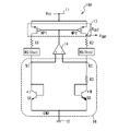
図1に示す一実施形態では、バンドギャップリファレンス回路100が、電源線11と、接地線12と、カレントミラー13と、演算増幅器14と、抵抗素子R1、R2、R3と、可変抵抗素子R4と、バイポーラトランジスタQ1、Q2とを備えている。電源線11には電源電圧Vccが供給され、接地線12は、接地されている。
In one embodiment shown in FIG. 1, the
カレントミラー13は、電流I1、I2の電流レベルが同一であるように電流I1、I2を出力する。本実施形態では、カレントミラー13が、1対のPMOSトランジスタMP1、MP2を備えている。PMOSトランジスタMP1、MP2は、ゲートが互いに接続され、更にソースが共通に電源線11に接続されている。PMOSトランジスタMP1のドレインは、抵抗素子R1を介してノードN1に接続され、PMOSトランジスタMP2のドレインは、抵抗素子R2を介してノードN2に接続されている。PMOSトランジスタMP1のドレインは、電流I1を出力する第1出力として用いられ、PMOSトランジスタMP2のドレインは、電流I2を出力する第2出力として用いられる。一実施形態では、抵抗素子R1、R2は、それらの抵抗が同一であるように設計される。
The
演算増幅器14は、非反転入力がノードN1に接続されており、反転入力がノードN2に接続されており、出力がPMOSトランジスタMP1、MP2のゲートに接続されている。演算増幅器14は、電流I1、I2を制御する制御電圧をカレントミラー13のPMOSトランジスタMP1、MP2のゲートに供給する。演算増幅器14は、ノードN1、N2が同一の電位を有するようにPMOSトランジスタMP1、MP2のゲートの電位を制御する。ノードN1、N2は、このような演算増幅器14の動作によって仮想ショートされる(virtually shorted)。カレントミラー13及び演算増幅器14は、総合すると、ノードN1、N2を同一の電位に制御すると共に、ノードN1、N2に同一電流レベルの電流を供給する電流供給回路部として動作することになる。
In the
バイポーラトランジスタQ1は、ダイオード接続されており、pn接合を有する第1のpn接合素子として動作する。本実施形態では、バイポーラトランジスタQ1としてNPNトランジスタが用いられている。バイポーラトランジスタQ1は、コレクタ及びベースが、ノードN1に共通に接続され、エミッタが接地線12に接続されている。このような接続により、電流I1は、バイポーラトランジスタQ1のベース-エミッタ間のpn接合を順方向に流れることになる。
The bipolar transistor Q1 is diode-connected and operates as a first pn junction element having a pn junction. In this embodiment, an NPN transistor is used as the bipolar transistor Q1. In the bipolar transistor Q1, the collector and the base are commonly connected to the node N1, and the emitter is connected to the
バイポーラトランジスタQ2と抵抗素子R3と可変抵抗素子R4とが、ノードN2と接地線12との間に直列に接続されている。図1においては、可変抵抗素子R4の抵抗が電源電圧Vccに依存することを明確にするために、可変抵抗素子R4が記号“R4(Vcc)”で示されている。なお、バイポーラトランジスタQ2、抵抗素子R3及び可変抵抗素子R4が接続される順序は、適宜に変更可能である。
The bipolar transistor Q2, the resistance element R3, and the variable resistance element R4 are connected in series between the node N2 and the
バイポーラトランジスタQ2も、バイポーラトランジスタQ1と同様にダイオード接続されており、第2のpn接合素子として動作する。本実施形態では、バイポーラトランジスタQ2としてNPNトランジスタが用いられている。バイポーラトランジスタQ2のベース-エミッタ接合の面積は、バイポーラトランジスタQ1のベース-エミッタ接合の面積のN倍である。ここで、Nは、1より大きい数である。本実施形態では、バイポーラトランジスタQ2は、コレクタ及びベースが、抵抗素子R3及び可変抵抗素子R4を介してノードN2に共通に接続され、エミッタが接地線12に接続されている。このような接続により、電流I2は、バイポーラトランジスタQ2のベース-エミッタ間のpn接合を順方向に流れることになる。
The bipolar transistor Q2 is also diode-connected like the bipolar transistor Q1 and operates as a second pn junction element. In this embodiment, an NPN transistor is used as the bipolar transistor Q2. The area of the base-emitter junction of the bipolar transistor Q2 is N times the area of the base-emitter junction of the bipolar transistor Q1. Here, N is a number larger than 1. In the present embodiment, in the bipolar transistor Q2, the collector and the base are commonly connected to the node N2 via the resistance element R3 and the variable resistance element R4, and the emitter is connected to the
なお、バイポーラトランジスタQ1、Q2としては、ダイオード接続されたPNPトランジスタが用いられてもよい。 As the bipolar transistors Q1 and Q2, diode-connected PNP transistors may be used.
一実施形態では、MOSトランジスタと共に形成される寄生バイポーラトランジスタが、バイポーラトランジスタQ1、Q2として用いられ得る。このような構成は、バンドギャップリファレンス回路100を、MOSトランジスタが集積化される集積回路に集積することを容易にする。
In one embodiment, the parasitic bipolar transistor formed with the MOS transistor can be used as the bipolar transistors Q1 and Q2. Such a configuration facilitates integration of the
ダイオード接続されたバイポーラトランジスタQ1、Q2の代わりに、pn接合を有する他の素子を用いてもよい。例えば、一実施形態では、半導体基板に形成されたウェルと該ウェルに形成された拡散層とを備えるダイオードがバイポーラトランジスタQ1、Q2の代わりに用いられてもよい。他の実施形態では、ダイオード接続されたバイポーラトランジスタQ1、Q2の代わりに、ダイオード接続されたMOSトランジスタが用いられてもよい。 Instead of the diode-connected bipolar transistors Q1 and Q2, another element having a pn junction may be used. For example, in one embodiment, a diode having a well formed in the semiconductor substrate and a diffusion layer formed in the well may be used instead of the bipolar transistors Q1 and Q2. In another embodiment, a diode-connected MOS transistor may be used instead of the diode-connected bipolar transistors Q1 and Q2.
可変抵抗素子R4は、電源線11に供給される電源電圧Vccに依存する抵抗を有している。一実施形態では、図2に図示されているように、可変抵抗素子R4として、ゲートに電源電圧Vccが供給されたNMOSトランジスタMN1が用いられてもよい。ゲートに電源電圧Vccが供給されているNMOSトランジスタMN1のオン抵抗は、電源電圧Vccに依存するので、NMOSトランジスタMN1は、可変抵抗素子R4として用いられ得る。この場合、可変抵抗素子R4の抵抗は、電源電圧Vccが増大すると減少する。可変抵抗素子R4として用いられるNMOSトランジスタのゲートに、電源電圧Vccの代わりに、電源電圧Vccから例えば電圧分圧によって生成されたバイアス電圧が供給されてもよい。他の実施形態では、可変抵抗素子R4として、PMOSトランジスタが用いられてもよい。
The variable resistance element R4 has a resistance depending on the power supply voltage Vcc supplied to the
本実施形態では、バンドギャップリファレンス回路100の出力電圧Voutは、PMOSトランジスタMP2のドレインと抵抗素子R2とを接続する出力ノードNoutから出力される。このような構成では、出力電圧Voutは、バイポーラトランジスタQ2のベース-エミッタ電圧VBE2と、抵抗素子R2、R3、可変抵抗素子R4における電圧降下の和として生成される。以下に議論するように、抵抗素子R2、R3、可変抵抗素子R4を流れる電流I2が、正の温度依存性を有する一方で、バイポーラトランジスタQ2のベース-エミッタ電圧VBE2は、絶対温度Tに対して負の温度依存性を有している。このため、バンドギャップリファレンス回路100の出力電圧Voutは、絶対温度Tに対して温度依存性が小さい。詳細には、バンドギャップリファレンス回路100は、以下のように動作して出力電圧Voutを生成する。
In the present embodiment, the output voltage Vout of the
バイポーラトランジスタQ1、Q2、抵抗素子R3及び可変抵抗素子R4の作用により、ノードN1、N2に供給される電流I1、I2は、絶対温度に比例する。この意味で、バイポーラトランジスタQ1、Q2と抵抗素子R3と可変抵抗素子R4とを、総称して、PTAT(proportional to absolute temperature)電流生成回路部15と呼ぶことがある。
The currents I 1 and I 2 supplied to the nodes N1 and N2 by the action of the bipolar transistors Q1 and Q2, the resistance element R3 and the variable resistance element R4 are proportional to the absolute temperature. In this sense, the bipolar transistors Q1 and Q2, the resistance element R3, and the variable resistance element R4 may be collectively referred to as a PTAT (proportional to absolute temperature) current
詳細には、カレントミラー13によって電流I1、I2が同一の電流レベルIに制御される場合、バイポーラトランジスタQ2のベース-エミッタ接合の面積がバイポーラトランジスタQ1のベース-エミッタ接合の面積のN倍であることから、バイポーラトランジスタQ1のベース-エミッタ電圧VBE1と、バイポーラトランジスタQ2のベース-エミッタ電圧VBE2とについて、例えば下記式(1a)(1b)が成立する。

ノードN1とノードN2が仮想ショートされており、ノードN2の電圧が、バイポーラトランジスタQ1のベース-エミッタ電圧VBE1に一致することから、下記式(2)が成立する:

式(1a)、(1b)を式(2)に代入することにより、電流I1、I2の電流レベルIが下記式(3)として得られる:


出力電圧Voutは、抵抗素子R2、R3及び可変抵抗素子R4で発生する電圧降下とバイポーラトランジスタQ2のベース-エミッタ電圧VBE2との和であり、例えば下記式(5)で表される:

加えて、式(5)からも理解されるように、可変抵抗素子R4を設けない場合のバンドギャップリファレンス回路100の出力電圧Voutの電源電圧Vccに対する依存性に応じて可変抵抗素子R4の特性を選択することで、出力電圧Voutの電源電圧Vccに対する依存性を低減できる。可変抵抗素子R4を設けない場合、出力電圧Voutは、電源電圧Vccの増加に伴って増加することが多い。この場合には、電源電圧Vccが増加したときに抵抗が増大するような可変抵抗素子R4を用いることで、出力電圧Voutの電源電圧Vccに対する依存性を低減することができる。逆に、可変抵抗素子R4を設けない場合に出力電圧Voutが電源電圧Vccの増加に伴って減少する場合には、電源電圧Vccが増加したときに抵抗が減少するような可変抵抗素子R4を用いることで、出力電圧Voutの電源電圧Vccに対する依存性を低減することができる。
In addition, as can be understood from the equation (5), the characteristics of the variable resistance element R4 are determined according to the dependence of the output voltage Vout of the
図3に示す一実施形態では、バンドギャップリファレンス回路100が、図1に示された構成と類似した構成となっている。ただし、可変抵抗素子R4を含んでいないPTAT電流生成回路部16が用いられると共に、出力ノードNoutとノードN2の間に抵抗素子R2と可変抵抗素子R5が直列に接続されている。
In one embodiment shown in FIG. 3, the
可変抵抗素子R4と同様に、可変抵抗素子R5としては、ゲートに電源電圧Vccが供給されたNMOSトランジスタが用いられてもよい(図2参照)。この場合、可変抵抗素子R5の抵抗は、電源電圧Vccが増大すると減少する。可変抵抗素子R5として用いられるNMOSトランジスタのゲートに、電源電圧Vccの代わりに、電源電圧Vccから例えば電圧分圧によって生成されたバイアス電圧が供給されてもよい。他の実施形態では、可変抵抗素子R5として、PMOSトランジスタが用いられてもよい。なお、抵抗素子R2と可変抵抗素子R5の位置は、交換可能である。 Similar to the variable resistance element R4, as the variable resistance element R5, an µtransistor to which a power supply voltage Vcc is supplied to the gate may be used (see FIG. 2). In this case, the resistance of the variable resistance element R5 decreases as the power supply voltage Vcc increases. Instead of the power supply voltage Vcc, a bias voltage generated by, for example, voltage division may be supplied from the power supply voltage Vcc to the gate of the µtransistor used as the variable resistance element R5. In other embodiments, a polyclonal transistor may be used as the variable resistance element R5. The positions of the resistance element R2 and the variable resistance element R5 are interchangeable.
図2に示す構成では、ノードN2の電圧が、バイポーラトランジスタQ1のベース-エミッタ電圧VBE1に一致することから、下記式(6):


出力電圧Voutは、例えば下記式(8)で表されるように、抵抗素子R2、可変抵抗素子R5及び抵抗素子R3で発生する電圧降下とバイポーラトランジスタQ2のベース-エミッタ電圧VBE2との和であり、N、R2、R3及びR5(Vcc)を適正に調節することにより、温度依存性の少ない又は全くない出力電圧Voutを実現できる。

また、可変抵抗素子R5を設けない場合のバンドギャップリファレンス回路100の出力電圧Voutの電源電圧Vccに対する依存性に応じて、出力電圧Voutの電源電圧Vccに対する依存性を低減するように、可変抵抗素子R5の特性を選択してもよい。可変抵抗素子R5を設けない場合、出力電圧Voutは、電源電圧Vccの増加に伴って増加することが多い。この場合には、電源電圧Vccが増加したときに抵抗が減少するような可変抵抗素子R5を用いることで、出力電圧Voutの電源電圧Vccに対する依存性を低減することができる。逆に、可変抵抗素子R5を設けない場合に出力電圧Voutが電源電圧Vccの増加に伴って減少する場合には、電源電圧Vccが増加したときに抵抗が減少するような可変抵抗素子R5を用いることで、出力電圧Voutの電源電圧Vccに対する依存性を低減することができる。
Further, the variable resistance element so as to reduce the dependence of the output voltage Vout on the power supply voltage Vcc according to the dependence of the output voltage Vout of the
図4に示す一実施形態では、バンドギャップリファレンス回路100が、図3に示された構成と類似した構成となっているが、PMOSトランジスタMP1のドレインとノードN1の間に、抵抗素子R1と可変抵抗素子R5が直列に接続されている。図3の構成では、PMOSトランジスタMP1、MP2のドレインに接続される抵抗素子の抵抗が相違しているため、アーリ効果に起因して電流I1、I2の電流レベルが相違し得る。一方で、図4の構成によれば、回路の対称性を高め、PMOSトランジスタMP1、MP2のアーリ効果に起因する電流I1、I2の電流レベルの差を有効に低減することができる。なお、抵抗素子R1と可変抵抗素子R5の位置は交換可能である。
In one embodiment shown in FIG. 4, the
図5に示す一実施形態では、バンドギャップリファレンス回路100が、図1に示す構成と図4に示す構成の組み合わせとして構成される。図5の構成では、可変抵抗素子R4を含んでいるPTAT電流生成回路部15が用いられる。加えて、PMOSトランジスタMP1のドレインとノードN1の間に抵抗素子R1と可変抵抗素子R5が直列に接続され、PMOSトランジスタMP2のドレインとノードN2の間に抵抗素子R2と可変抵抗素子R5が直列に接続されている。
In one embodiment shown in FIG. 5, the
図5の構成では、出力電圧Voutは、抵抗素子R2、可変抵抗素子R5、可変抵抗素子R4及び抵抗素子R3で発生する電圧降下とバイポーラトランジスタQ2のベース-エミッタ電圧VBE2との和であり、例えば下記式(9)で表される:

式(9)に基づき、一実施形態では、N、R2、R3、R4(Vcc)及びR5(Vcc)が、温度依存性が小さい又は全くない出力電圧Voutを生成するように調節される。 Based on formula (9), in one embodiment, N, R2, R3, R4 (Vcc) and R5 (Vcc) are adjusted to produce an output voltage Vout with little or no temperature dependence.
また、可変抵抗素子R4、R5の特性は、可変抵抗素子R4、R5を設けない場合のバンドギャップリファレンス回路100の出力電圧Voutの電源電圧Vccに対する依存性に応じて、出力電圧Voutの電源電圧Vccに対する依存性を低減するように選択される。
Further, the characteristics of the variable resistance elements R4 and R5 are such that the power supply voltage Vcc of the output voltage Vout depends on the dependence of the output voltage Vout of the
図6に示す一実施形態では、バンドギャップリファレンス回路200が、電源線21と、接地線22と、カレントミラー23と、演算増幅器24と、抵抗素子R3、R6、R7、R8と、可変抵抗素子R4と、バイポーラトランジスタQ1、Q2とを備えている。電源線21には電源電圧Vccが供給され、接地線22は、接地されている。
In one embodiment shown in FIG. 6, the
カレントミラー23は、電流I1、I2の電流レベルが同一であるように電流I1、I2を出力する。加えて、カレントミラー23は、電流I1、I2の電流レベルに比例する電流レベルを有する電流I0を出力する。一実施形態では、カレントミラー23は、電流I0の電流レベルが、電流I1、I2の電流レベルと同じであるように電流I0を出力してもよい。本実施形態では、カレントミラー23が、PMOSトランジスタMP0、MP1及びMP2を備えている。PMOSトランジスタMP0、MP1及びMP2は、ゲートが互いに接続され、更にソースが共通に電源線21に接続されている。PMOSトランジスタMP1のドレインは、ノードN1に接続され、PMOSトランジスタMP2のドレインは、ノードN2に接続されている。PMOSトランジスタMP0のドレインは、出力ノードNoutに接続されている。
The
演算増幅器24は、非反転入力がノードN1に接続されており、反転入力がノードN2に接続されており、出力がPMOSトランジスタMP1、MP2のゲートに接続されている。演算増幅器24は、電流I1、I2、I0を制御する制御電圧をカレントミラー13のPMOSトランジスタMP1、MP2、MP0のゲートに出力する。演算増幅器14は、ノードN1、N2が同一の電位を有するようにPMOSトランジスタMP1、MP2のゲートの電位を制御する。ノードN1、N2は、このような演算増幅器24の動作により、仮想ショートされる。カレントミラー23及び演算増幅器24は、総合すると、ノードN1、N2を同一の電位に制御すると共に、ノードN1、N2に同一電流レベルの電流を供給する電流供給回路部として動作することになる。
In the
図1に示したバンドギャップリファレンス回路100と同様に、本実施形態でも、バイポーラトランジスタQ1、Q2、抵抗素子R3及び可変抵抗素子R4が、PTAT電流生成回路部25として動作する。バイポーラトランジスタQ1は、ノードN1と接地線22の間に接続されている。抵抗素子R3、バイポーラトランジスタQ2及び可変抵抗素子R4は、ノードN1と接地線22の間に直列に接続されている。バイポーラトランジスタQ2のベース-エミッタ接合の面積は、バイポーラトランジスタQ1のベース-エミッタ接合の面積のN倍である。なお、抵抗素子R3、バイポーラトランジスタQ2及び可変抵抗素子R4が接続される順序は、順不同である。
Similar to the
抵抗素子R6は、ノードN1と接地線22の間に、バイポーラトランジスタQ1と並列に接続されており、抵抗素子R7は、ノードN2と接地線22の間に、抵抗素子R3、バイポーラトランジスタQ2及び可変抵抗素子R4と並列に接続されている。一実施形態では、抵抗素子R6、R7は、同一の抵抗を有するように設計される。
The resistance element R6 is connected in parallel with the bipolar transistor Q1 between the node N1 and the
抵抗素子R8は、出力ノードNoutと接地線22の間に接続されている。抵抗素子R8は、出力ノードNoutに供給される電流I0から出力電圧Voutを生成する電流-電圧変換回路部として機能する。
The resistance element R8 is connected between the output node Nout and the
本実施形態のバンドギャップリファレンス回路200は、概略的には、下記の動作によって温度依存性が小さい出力電圧Voutを生成する。バイポーラトランジスタQ1を流れる電流I1A及び抵抗素子R3、バイポーラトランジスタQ2及び可変抵抗素子R4を流れる電流I2Aは、いずれも、正の温度依存性を有するPTAT電流である。一方、抵抗素子R6を流れる電流I1B及び抵抗素子R7を流れる電流I2Bは、負の温度依存性を有するCTAT(complementary to absolute temperature)電流である。電流I1は、電流I1Aと電流I1Bの和電流であり、電流I2は、電流I2Aと電流I2Bの和電流であるから、電流I1、I2の温度依存性を小さくすることができる。よって、電流I1、I2のミラーリングにより生成される電流I0も温度依存性を小さくすることができる。出力電圧Voutは、電流I0が抵抗素子R8を流れることで発生する電位差として生成されるので、出力電圧Voutの温度依存性も低減される。詳細には、バンドギャップリファレンス回路100の出力電圧Voutは、以下のように得られる。
The
ノードN2に流れ込む電流I2は、電流I2Aと電流I2Bの和電流であるから、下記式(10)が成立する。

ノードN1、N2が仮想ショートされることから、ノードN2の電位は、バイポーラトランジスタQ1のベース-エミッタ電圧VBE1になり、よって、電流I2A、I2Bは、下記式(11a)、(11b)で表される。

ベース-エミッタ電圧VBE1、VBE2を表す式(1a)、(1b)と、式(10)、(11a)、(11b)から、電流I2は、下記式(12)として表される:

カレントミラー23が、電流I2と同一の電流レベルを有するように電流I3を出力する場合、出力電圧Voutは、例えば下記式(13)で表される:

熱電圧Vtが温度に比例して増加する正の温度依存性を有する一方で、ベース-エミッタ電圧VBE1が負の温度依存性を有しているから、式(13)からも理解されるように、N、R2、R3、R4(Vcc)及びR7を調節することにより、出力電圧Voutの温度依存性を低減することができる。 As can be understood from Eq. (13), since the base-emitter voltage VBE1 has a negative temperature dependence while the thermal voltage Vt has a positive temperature dependence that increases in proportion to the temperature. In addition, by adjusting N, R2, R3, R4 (Vcc) and R7, the temperature dependence of the output voltage Vout can be reduced.
また、可変抵抗素子R4を設けない場合のバンドギャップリファレンス回路200の出力電圧Voutの電源電圧Vccに対する依存性に応じて可変抵抗素子R4の特性を選択することで、出力電圧Voutの電源電圧Vccに対する依存性を低減できる。
Further, by selecting the characteristics of the variable resistance element R4 according to the dependence of the output voltage Vout of the
図7に示す一実施形態では、バンドギャップリファレンス回路200が、図6に示された構成と類似した構成となっている。ただし、可変抵抗素子R4を含んでいないPTAT電流生成回路部26が用いられると共に、出力ノードNoutと接地線22の間に抵抗素子R8と可変抵抗素子R5とが直列に接続された電流-電圧変換回路部27が接続される。
In one embodiment shown in FIG. 7, the
図7に図示されているバンドギャップリファレンス回路200では、電流I2は、例えば下記式(14)で表される。

よって、出力電圧Voutは、例えば下記式(15)で表される。

式(15)からも理解されるように、N、R2、R3及びR7を適正に調節することにより、出力電圧Voutの温度依存性を低減することができる。 As can be understood from the equation (15), the temperature dependence of the output voltage Vout can be reduced by appropriately adjusting N, R2, R3 and R7.
また、可変抵抗素子R5を設けない場合のバンドギャップリファレンス回路200の出力電圧Voutの電源電圧Vccに対する依存性に応じて可変抵抗素子R5の特性を適切に選択することで、出力電圧Voutの電源電圧Vccに対する依存性を低減できる。
Further, by appropriately selecting the characteristics of the variable resistance element R5 according to the dependence of the output voltage Vout of the
図8に示す一実施形態では、バンドギャップリファレンス回路200が、図6に示す構成と図7に示す構成の組み合わせとして構成される。図8の構成では、可変抵抗素子R4を含んでいるPTAT電流生成回路部25が用いられる。加えて、出力ノードNoutと接地線22の間に抵抗素子R8と可変抵抗素子R5とが直列に接続された電流-電圧変換回路部27が接続される。
In one embodiment shown in FIG. 8, the
図8の構成では、出力電圧Voutは、例えば、下記式(16)で表される:

式(16)に基づき、一実施形態では、N、R3、R4(Vcc)及びR7が、温度依存性が小さい又は全くない出力電圧Voutを生成するように調節される。 Based on equation (16), in one embodiment, N, R3, R4 (Vcc) and R7 are adjusted to produce an output voltage Vout with little or no temperature dependence.
また、可変抵抗素子R4、R5の特性は、可変抵抗素子R4、R5を設けない場合のバンドギャップリファレンス回路200の出力電圧Voutの電源電圧Vccに対する依存性に応じて、出力電圧Voutの電源電圧Vccに対する依存性を低減するように調節される。
Further, the characteristics of the variable resistance elements R4 and R5 are such that the power supply voltage Vcc of the output voltage Vout depends on the dependence of the output voltage Vout of the
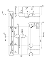
図9に示す一実施形態では、バンドギャップリファレンス回路300が、電源線31と、接地線32と、カレントミラー33と、演算増幅器34-1、34-2と、抵抗素子R3と、可変抵抗素子R4と、バイポーラトランジスタQ1、Q2、Q3と、電流-電圧変換回路部36とを備えている。電源線31には電源電圧Vccが供給され、接地線32は、接地されている。
In one embodiment shown in FIG. 9, the band
カレントミラー33は、電流I0、I1、I2、I3の電流レベルが同一であるように電流I0、I1、I2、I3を出力する。本実施形態では、カレントミラー33が、PMOSトランジスタMP0、MP1、MP2及びMP3を備えている。PMOSトランジスタMP0、MP1、MP2及びMP3は、ゲートが互いに接続され、更にソースが共通に電源線31に接続されている。PMOSトランジスタMP1、MP2、MP3のドレインは、それぞれ、ノードN1、N2、N3に接続されている。PMOSトランジスタMP0のドレインは、出力ノードNoutに接続されている。
The
バイポーラトランジスタQ1、Q2、Q3は、それぞれ、pn接合を有する第1、第2及び第3のpn接合素子として動作する。本実施形態では、バイポーラトランジスタQ1、Q2、Q3としてNPNトランジスタが用いられる。バイポーラトランジスタQ1、Q2、Q3のベースは、バイポーラトランジスタQ3のコレクタに共通に接続されている。バイポーラトランジスタQ1、Q2、Q3のコレクタは、それぞれ、ノードN1、N2、N3に接続されている。バイポーラトランジスタQ1、Q3のエミッタは、接地線32に接続されており、バイポーラトランジスタQ2のエミッタは、抵抗素子R3及び可変抵抗素子R4を介して接地線32に接続されている。このような接続により、電流I1、I2、I3は、それぞれ、バイポーラトランジスタQ1、Q2、Q3のベース-エミッタ間のpn接合の順方向に流れることになる。
The bipolar transistors Q1, Q2, and Q3 operate as first, second, and third pn junction elements having a pn junction, respectively. In this embodiment, NPN transistors are used as the bipolar transistors Q1, Q2, and Q3. The bases of the bipolar transistors Q1, Q2, and Q3 are commonly connected to the collector of the bipolar transistor Q3. The collectors of the bipolar transistors Q1, Q2, and Q3 are connected to the nodes N1, N2, and N3, respectively. The emitters of the bipolar transistors Q1 and Q3 are connected to the
本実施形態では、バイポーラトランジスタQ1、Q3のベース-エミッタ接合の面積が同一であり、バイポーラトランジスタQ2のベース-エミッタ接合の面積は、バイポーラトランジスタQ1、Q3のベース-エミッタ接合の面積のN倍である。ここで、Nは、1より大きい数である。 In the present embodiment, the area of the base-emitter junction of the bipolar transistors Q1 and Q3 is the same, and the area of the base-emitter junction of the bipolar transistor Q2 is N times the area of the base-emitter junction of the bipolar transistors Q1 and Q3. be. Here, N is a number larger than 1.
演算増幅器34-1は、反転入力がノードN1に接続されており、非反転入力がノードN2に接続されており、出力がPMOSトランジスタMP0、MP1、MP2、MP3のゲートに接続されている。演算増幅器34-1は、電流I1、I2を制御する制御電圧をカレントミラー33のPMOSトランジスタMP1、MP2のゲートに出力する。
In the operational amplifier 34-1, the inverting input is connected to the node N1, the non-inverting input is connected to the node N2, and the output is connected to the gates of the polyclonal transistors MP0, MP1, MP2, MP3. The operational amplifier 34-1 outputs a control voltage for controlling the currents I 1 and I 2 to the gates of the polyclonal transistors MP1 and MP2 of the
演算増幅器34-2は、反転入力がノードN3に接続されており、非反転入力がノードN1に接続されており、出力がバイポーラトランジスタQ1、Q2、Q3のベースに接続されている。演算増幅器34-2は、電流I1、I3を制御する制御電圧をバイポーラトランジスタQ1、Q2、Q3のベースに出力する。 In the operational amplifier 34-2, the inverting input is connected to the node N3, the non-inverting input is connected to the node N1, and the output is connected to the base of the bipolar transistors Q1, Q2, and Q3. The operational amplifier 34-2 outputs the control voltage for controlling the currents I 1 and I 3 to the base of the bipolar transistors Q1, Q2 and Q3.
演算増幅器34-1、34-2は、全体としては、ノードN1、N2、N3が同一の電位を有するようにPMOSトランジスタMP1、MP2、MP3のゲートの電位及びバイポーラトランジスタQ1、Q2、Q3のベースの電位を制御することになる。ノードN1、N2、N3は、このような演算増幅器34-1、34-2の動作によって仮想ショートされる。カレントミラー33、演算増幅器34-1及び34-2は、総合すると、ノードN1、N2、N3を同一の電位に制御すると共に、ノードN1、N2、N3に同一電流レベルの電流を供給する電流供給回路部として動作することになる。
The arithmetic amplifiers 34-1 and 34-2 have the potentials of the gates of the polyclonal transistors MP1, MP2 and MP3 and the bases of the bipolar transistors Q1, Q2 and Q3 so that the nodes N1, N2 and N3 have the same potential as a whole. Will control the potential of. The nodes N1, N2, and N3 are virtually short-circuited by the operation of the operational amplifiers 34-1 and 34-2. The
電流-電圧変換回路部36は、カレントミラー33から受け取った電流I0から出力電圧Voutを生成する。本実施形態では、電流-電圧変換回路部36は、ダイオード接続されたバイポーラトランジスタQ0と、抵抗素子R9、R10とを備えている。バイポーラトランジスタQ0のベース-エミッタ接合の面積は、バイポーラトランジスタQ1、Q3のベース-エミッタ接合の面積と同じである。バイポーラトランジスタQ0と抵抗素子R9とは、出力ノードNoutと接地線32の間に直列に接続されている。なお、バイポーラトランジスタQ0と抵抗素子R9の位置は、交換可能である。抵抗素子R10は、出力ノードNoutと接地線32の間に、バイポーラトランジスタQ0及び抵抗素子R9と並列に接続されている。
The current-voltage
本実施形態のバンドギャップリファレンス回路300は、概略的には、下記の原理により、温度依存性が小さい出力電圧Voutを生成可能である。バイポーラトランジスタQ1を流れる電流I1、バイポーラトランジスタQ2、抵抗素子R3及び可変抵抗素子R4を流れる電流I2を流れる電流は、正の温度依存性を有するPTAT電流である。この意味で、バイポーラトランジスタQ1、Q2と抵抗素子R3と可変抵抗素子R4とを、総称して、PTAT電流生成回路部35と呼ぶことがある。
The
電流-電圧変換回路部36に供給される電流I0は、電流I1、I2と同一の電流レベルIを有しているから、電流I0もPTAT電流である。電流-電圧変換回路部36は、電流I0を、正の温度依存性を有する電流I0Aと温度依存性が小さい電流I0Bに分流し、電流I0Bが抵抗素子R10に流れることで発生する電圧を、出力電圧Voutとして出力する。よって、バンドギャップリファレンス回路300は、出力電圧Voutの温度依存性を小さくすることができる。詳細には、バンドギャップリファレンス回路300は、以下のように動作して出力電圧Voutを生成する。
Since the current I 0 supplied to the current-voltage
本実施形態においては、電流I1、I2、I0の電流レベルIは、同一であり、下記式(17)で表される。

また、電流I0は、電流I1、I2と同一の電流レベルIを有し、且つ、バイポーラトランジスタQ0及び抵抗素子R9を流れる電流I0Aと抵抗素子R10を流れる電流I0Bの和電流であるから、下記式(18)が成立する:

また、バイポーラトランジスタQ0のベース-エミッタ電圧VBE0、抵抗素子R9及びR10の電圧降下について、下記式(19)が成立する:

式(17)~(19)から、電流I0Bは、下記式(20)により表される:

出力電圧Voutは、例えば下記式(21)により表される:

熱電圧Vtが温度に比例して増加する正の温度依存性を有する一方で、ベース-エミッタ電圧VBE0が負の温度依存性を有しているから、N、R3、R4(Vcc)及びR9を適正に調節することにより、出力電圧Voutの温度依存性を低減することができる。 Since the thermal voltage Vt has a positive temperature dependence that increases in proportion to the temperature, while the base-emitter voltage VBE0 has a negative temperature dependence, N, R3, R4 (Vcc) and R9. By properly adjusting the temperature, the temperature dependence of the output voltage Vout can be reduced.
加えて、式(21)からも理解されるように、可変抵抗素子R4を設けない場合のバンドギャップリファレンス回路300の出力電圧Voutの電源電圧Vccに対する依存性に応じて可変抵抗素子R4の特性を適切に選択することで、出力電圧Voutの電源電圧Vccに対する依存性を低減できる。
In addition, as can be understood from the equation (21), the characteristics of the variable resistance element R4 are determined according to the dependence of the output voltage Vout of the
図10に示す一実施形態では、バンドギャップリファレンス回路300が、図9に示された構成と類似した構成となっている。ただし、可変抵抗素子R4を含んでいないPTAT電流生成回路部37が用いられると共に、バイポーラトランジスタQ0と抵抗素子R9とに可変抵抗素子R5が直列に接続された電流-電圧変換回路38が用いられる。なお、バイポーラトランジスタQ0と抵抗素子R9と可変抵抗素子R5が接続される順序は、順不同である。
In one embodiment shown in FIG. 10, the
本実施形態においては、電流I1、I2、I0の電流レベルIは、同一であり、下記式(22)で表される。

また、バイポーラトランジスタQ0のベース-エミッタ電圧VBE0、抵抗素子R9及びR10の電圧降下について、下記式(23)が成立する:

式(18)、(22)、(23)から、電流I0Bは、下記式(24)により表される:

出力電圧Voutは、例えば下記式(25)により表される:

熱電圧Vtが温度に比例して増加する正の温度依存性を有する一方で、ベース-エミッタ電圧VBE1が負の温度依存性を有しているから、式(25)からも理解されるように、N、R3、R9及びR5(Vcc)を適正に調節することにより、出力電圧Voutの温度依存性を低減することができる。 As can be understood from Eq. (25), since the base-emitter voltage VBE1 has a negative temperature dependence while the thermal voltage Vt has a positive temperature dependence that increases in proportion to the temperature. In addition, by appropriately adjusting N, R3, R9 and R5 (Vcc), the temperature dependence of the output voltage Vout can be reduced.
また、可変抵抗素子R5を設けない場合のバンドギャップリファレンス回路300の出力電圧Voutの電源電圧Vccに対する依存性に応じて可変抵抗素子R5の特性を適切に選択することで、出力電圧Voutの電源電圧Vccに対する依存性を低減できる。
Further, by appropriately selecting the characteristics of the variable resistance element R5 according to the dependence of the output voltage Vout of the
図11に示す一実施形態では、バンドギャップリファレンス回路300が、図9に示す構成と図10に示す構成の組み合わせとして構成される。図11の構成では、可変抵抗素子R4を含んでいるPTAT電流生成回路部35が用いられる。加えて、バイポーラトランジスタQ0と抵抗素子R9とに可変抵抗素子R5が直列に接続された電流-電圧変換回路38が用いられる。
In one embodiment shown in FIG. 11, the
図11の構成では、出力電圧Voutは、例えば下記式(26)により表される:

式(26)に基づき、一実施形態では、N、R3、R4(Vcc)、R5(Vcc)及びR9が、温度依存性が小さい又は全くない出力電圧Voutを生成するように調節される。 Based on equation (26), in one embodiment, N, R3, R4 (Vcc), R5 (Vcc) and R9 are adjusted to produce an output voltage Vout with little or no temperature dependence.
また、可変抵抗素子R4、R5の特性は、可変抵抗素子R4、R5を設けない場合のバンドギャップリファレンス回路300の出力電圧Voutの電源電圧Vccに対する依存性に応じて、出力電圧Voutの電源電圧Vccに対する依存性を低減するように選択される。
Further, the characteristics of the variable resistance elements R4 and R5 are such that the power supply voltage Vcc of the output voltage Vout depends on the dependence of the output voltage Vout of the
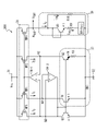
図12に示す一実施形態では、バンドギャップリファレンス回路400が、電源線41と、接地線42と、カレントミラー43と、演算増幅器44と、抵抗素子R3と、可変抵抗素子R4と、バイポーラトランジスタQ1、Q2、Q3と、電流-電圧変換回路部46と、カレントミラー47と、演算増幅器48とを備えている。電源線41には電源電圧Vccが供給され、接地線42は、接地されている。
In one embodiment shown in FIG. 12, the band
カレントミラー43は、電流I0、I1、I2、I3の電流レベルが同一であるように電流I0、I1、I2、I3を出力する。本実施形態では、カレントミラー43が、PMOSトランジスタMP0、MP1、MP2、MP3を備えている。PMOSトランジスタMP0、MP1、MP2、MP3は、ゲートが互いに接続され、更にソースが共通に電源線41に接続されている。PMOSトランジスタMP1、MP2、MP3のドレインは、それぞれ、ノードN1、N2、N3に接続されている。PMOSトランジスタMP0のドレインは、出力ノードNoutに接続されている。
The
バイポーラトランジスタQ1、Q2、Q3は、それぞれ、pn接合を有する第1、第2及び第3のpn接合素子として動作する。本実施形態では、バイポーラトランジスタQ1、Q2、Q3としてNPNトランジスタが用いられる。バイポーラトランジスタQ1、Q2、Q3のベースは、バイポーラトランジスタQ3のコレクタに共通に接続されている。バイポーラトランジスタQ1、Q2、Q3のコレクタは、それぞれ、ノードN1、N2、N3に接続されている。バイポーラトランジスタQ1、Q3のエミッタは、接地線42に接続されており、バイポーラトランジスタQ2のエミッタは、抵抗素子R3及び可変抵抗素子R4を介して接地線42に接続されている。このような接続により、電流I1、I2、I3は、それぞれ、バイポーラトランジスタQ1、Q2、Q3のベース-エミッタ間のpn接合の順方向に流れることになる。
The bipolar transistors Q1, Q2, and Q3 operate as first, second, and third pn junction elements having a pn junction, respectively. In this embodiment, NPN transistors are used as the bipolar transistors Q1, Q2, and Q3. The bases of the bipolar transistors Q1, Q2, and Q3 are commonly connected to the collector of the bipolar transistor Q3. The collectors of the bipolar transistors Q1, Q2, and Q3 are connected to the nodes N1, N2, and N3, respectively. The emitters of the bipolar transistors Q1 and Q3 are connected to the
本実施形態では、バイポーラトランジスタQ1、Q3のベース-エミッタ接合の面積が同一であり、バイポーラトランジスタQ2のベース-エミッタ接合の面積は、バイポーラトランジスタQ1、Q3のベース-エミッタ接合の面積のN倍である。ここで、Nは、1より大きい数である。 In the present embodiment, the area of the base-emitter junction of the bipolar transistors Q1 and Q3 is the same, and the area of the base-emitter junction of the bipolar transistor Q2 is N times the area of the base-emitter junction of the bipolar transistors Q1 and Q3. be. Here, N is a number larger than 1.
演算増幅器44は、非反転入力がノードN1に接続されており、反転入力がノードN2に接続されており、出力がPMOSトランジスタMP0、MP1、MP2、MP3のゲートに接続されている。演算増幅器44は、電流I0、I1、I2、I3を制御する制御電圧をカレントミラー13のPMOSトランジスタMP0、MP1、MP2、MP3のゲートに出力する。演算増幅器44は、ノードN1、N2が同一の電位を有するようにPMOSトランジスタMP0、MP1、MP2及びMP3のゲートの電位を制御する。ノードN1、N2は、このような演算増幅器44の動作によって仮想ショートされる。カレントミラー43及び演算増幅器44は、総合すると、ノードN1、N2を同一の電位に制御すると共に、ノードN1、N2に同一電流レベルの電流を供給する電流供給回路部として動作することになる。
In the
電流-電圧変換回路部46は、カレントミラー43から受け取った電流I0に応じて出力電圧Voutを生成する。本実施形態では、電流-電圧変換回路部46は、ダイオード接続されたバイポーラトランジスタQ0と、抵抗素子R9、R10とを備えている。バイポーラトランジスタQ0のベース-エミッタ接合の面積は、バイポーラトランジスタQ1、Q3のベース-エミッタ接合の面積と同じである。バイポーラトランジスタQ0と抵抗素子R9とは、出力ノードNoutと接地線42の間に直列に接続されている。なお、バイポーラトランジスタQ0と抵抗素子R9の位置は、交換可能である。抵抗素子R10は、出力ノードNoutと接地線42の間に、バイポーラトランジスタQ0及び抵抗素子R9と並列に接続されている。
The current-voltage
カレントミラー47は、電流I4をノードN3に出力すると共に、電流I5を電流-電圧変換回路部46に出力する。電流-電圧変換回路部46には、カレントミラー43からの電流I0とカレントミラー47からの電流I5の和電流が供給されることになる。カレントミラー47のミラー比は、A:1であり、電流I5は、電流I4の1/A倍である。本実施形態では、カレントミラー47が、PMOSトランジスタMP4、MP5を備えている。PMOSトランジスタMP4、MP5は、ゲートが互いに接続され、更にソースが共通に電源線41に接続されている。PMOSトランジスタMP4のドレインは、ノードN3に接続されており、PMOSトランジスタMP5のドレインは、電流-電圧変換回路部46に接続されている。一実施形態では、PMOSトランジスタMP4、MP5は、同一のゲート長Lを有しており、PMOSトランジスタMP4のゲート幅WMP4がPMOSトランジスタMP5のゲート幅WMP5のA倍であるように設計される。
The
演算増幅器48は、電流I4、I5を制御する制御電圧をカレントミラー47のPMOSトランジスタMP4、MP5のゲートに出力する。演算増幅器48は、ノードN2、N3が同一の電位を有するようにPMOSトランジスタMP4及びMP5のゲートの電位を制御する。ノードN2、N3は、演算増幅器48により仮想ショートされる。
The
本実施形態のバンドギャップリファレンス回路400は、下記のような動作により出力電圧Voutを出力する。
The
電流I1、I2、I3は、コレクタ電流としてバイポーラトランジスタQ1、Q2、Q3に供給される一方で、カレントミラー43により電流I1、I2、I3が、同一の電流レベルに制御されるから、カレントミラー47からノードN3に供給される電流I4は、バイポーラトランジスタQ1、Q2、Q3のベース電流の和電流である。よって、カレントミラー47から電流-電圧変換回路部46に供給される電流I5は、バイポーラトランジスタQ1、Q2、Q3のベース電流に依存する。
The currents I 1 , I 2 , and I 3 are supplied to the bipolar transistors Q1, Q2, and Q3 as collector currents, while the
一般に、エミッタ接地のバイポーラトランジスタでは、ベース電流がコレクタ電流と比較すると非常に小さいから、バイポーラトランジスタQ1、Q2、Q3のベース電流の和電流である電流I4は、バイポーラトランジスタQ1、Q2、Q3のコレクタ電流である電流I1、I2、I3に対して非常に小さいと考えてよい。ここで、電流I0の電流レベルは、電流I1、I2、I3と同一であり、電流I5は電流I4の1/A倍の電流レベルを有するから、電流I5は、電流I0に対して非常に小さいと考えてよい。
Generally, in a bipolar transistor with a grounded emitter, the base current is very small as compared with the collector current. Therefore, the current I4 , which is the sum of the base currents of the bipolar transistors Q1, Q2, and Q3, is the bipolar transistor Q1, Q2, and Q3. It can be considered that it is very small with respect to the collector currents I 1 , I 2 , and I 3 . Here, the current level of the current I 0 is the same as the currents I 1 , I 2 , and I 3 , and the current I 5 has a
この場合、バンドギャップリファレンス回路400の出力電圧Voutは、第1近似としては、図9に示したバンドギャップリファレンス回路300と同様に、例えば上記の式(21)で表される。よって、N、R3、R4(Vcc)及びR9を適正に調節することによって出力電圧Voutの温度依存性を低減することができる。加えて、可変抵抗素子R4を設けない場合のバンドギャップリファレンス回路400の出力電圧Voutの電源電圧Vccに対する依存性に応じて可変抵抗素子R4の特性を選択することによって出力電圧Voutの電源電圧Vccに対する依存性を低減できる。
In this case, the output voltage Vout of the
カレントミラー47から電流-電圧変換回路部46に供給される電流I5は、出力電圧Voutの非線形的な温度依存性を補償するために用いられる。式(21)からも理解されるように、出力電圧Voutはベース-エミッタ電圧VBE0に依存する。バイポーラトランジスタのベース-エミッタ電圧は、一般に、負の非線形的な温度依存性を有していることが知られている。一方で、熱電圧Vtは、絶対温度Tに比例し、線形的な温度依存性を有している。よって、電流I0のみを電流-電圧変換回路部46に供給する場合には、出力電圧Voutの非線形的な温度依存性は、完全には解消されない。一方で、電流I5は、バイポーラトランジスタQ1、Q2、Q3のベース電流に比例する電流レベルを有しており、よって、非線形的な温度依存性を有している。本実施形態では、電流I0に加えて電流I5を電流-電圧変換回路部46に供給することで、ベース-エミッタ電圧VBE0の非線形的な温度依存性を補償し、出力電圧Voutの温度依存性をより低減することができる。
The current I 5 supplied from the
図13に示す一実施形態では、バンドギャップリファレンス回路400が、図12に示された構成と類似した構成となっている。ただし、可変抵抗素子R4を含んでいないPTAT電流生成回路部49が用いられると共に、バイポーラトランジスタQ0と抵抗素子R9とに可変抵抗素子R5が直列に接続された電流-電圧変換回路50が用いられる。なお、バイポーラトランジスタQ0と抵抗素子R9と可変抵抗素子R5が接続される順序は、順不同である。
In one embodiment shown in FIG. 13, the
図13に示すバンドギャップリファレンス回路400についても、図12に示すバンドギャップリファレンス回路400と同様の議論が成立する。図13に示すバンドギャップリファレンス回路400の出力電圧Voutは、第1近似としては、図10に示したバンドギャップリファレンス回路300と同様に、例えば上記の式(25)で表される。よって、N、R3、R9及びR5(Vcc)を適正に調節することによって出力電圧Voutの温度依存性を低減することができる。また、可変抵抗素子R5を設けない場合のバンドギャップリファレンス回路400の出力電圧Voutの電源電圧Vccに対する依存性に応じて可変抵抗素子R5の特性を選択することで、出力電圧Voutの電源電圧Vccに対する依存性を低減できる。
Regarding the
図14に示す一実施形態では、バンドギャップリファレンス回路400が、図12に示す構成と図13に示す構成の組み合わせとして構成される。図14の構成では、可変抵抗素子R4を含んでいるPTAT電流生成回路部45が用いられる。加えて、バイポーラトランジスタQ0と抵抗素子R9とに可変抵抗素子R5が直列に接続された電流-電圧変換回路50が用いられる。
In one embodiment shown in FIG. 14, the
図14に示すバンドギャップリファレンス回路400についても、図12及び図13に示すバンドギャップリファレンス回路400と同様の議論が成立する。図14に示すバンドギャップリファレンス回路400の出力電圧Voutは、第1近似としては、図11に示したバンドギャップリファレンス回路300と同様に、例えば上記の式(26)で表される。式(26)に基づき、一実施形態では、N、R3、R4(Vcc)、R5(Vcc)及びR9が、温度依存性が小さい又は全くない出力電圧Voutを生成するように調節される。また、可変抵抗素子R4、R5の特性は、可変抵抗素子R4、R5を設けない場合のバンドギャップリファレンス回路300の出力電圧Voutの電源電圧Vccに対する依存性に応じて、出力電圧Voutの電源電圧Vccに対する依存性を低減するように選択される。
Regarding the
以上には、本開示の様々な実施形態が具体的に記載されているが、本開示に記載された技術は、様々な変更と共に実施され得る。 Although various embodiments of the present disclosure are specifically described above, the techniques described in the present disclosure may be implemented with various modifications.
100、200、300、400:バンドギャップリファレンス回路
11 :電源線
12 :接地線
13 :カレントミラー
14 :演算増幅器
15、16:PTAT電流生成回路部
21 :電源線
22 :接地線
23 :カレントミラー
24 :演算増幅器
25、26:PTAT電流生成回路部
27 :電流-電圧変換回路部
31 :電源線
32 :接地線
33 :カレントミラー
34-1、34-2:演算増幅器
35、37:PTAT電流生成回路部
36、38:電流-電圧変換回路部
41 :電源線
42 :接地線
43 :カレントミラー
44 :演算増幅器
45、49:PTAT電流生成回路部
46、50:電流-電圧変換回路部
47 :カレントミラー
48 :演算増幅器
MN1 :NMOSトランジスタ
MP0~MP5:PMOSトランジスタ
N1~N3:ノード
Nout :出力ノード
Q0~Q3:バイポーラトランジスタ
R1~R3、R6~R10:抵抗素子
R4、R5:可変抵抗素子
100, 200, 300, 400: Band gap reference circuit 11: Power supply line 12: Ground line 13: Current mirror 14:
Claims (20)
前記第2ノードと接地線の間の、前記電源線に供給される電源電圧に抵抗が依存するように構成された第1可変抵抗素子と、
を備える
バンドギャップリファレンス回路。 A first current mirror connected to a power line, supplying a first current to the first node, and supplying a second current to a second node virtually short-circuited with the first node.
A first variable resistance element between the second node and the ground line , configured so that the resistance depends on the power supply voltage supplied to the power supply line.
Bandgap reference circuit with .
前記第1ノードと前記接地線の間の第1pn接合素子と、The first pn junction element between the first node and the ground wire,
前記第1可変抵抗素子と直列に接続された第2pn接合素子と、A second pn junction element connected in series with the first variable resistance element and
を備えるEquipped with
請求項1に記載のバンドギャップリファレンス回路。The bandgap reference circuit according to claim 1.
請求項2に記載のバンドギャップリファレンス回路。 The bandgap reference circuit according to claim 2 , further comprising a first resistance element connected in series with the first variable resistance element and the second pn junction element between the second node and the ground wire.
前記第1カレントミラーが前記第1出力で前記第2電流を出力するように構成された
請求項2又は3に記載のバンドギャップリファレンス回路。 Further, a second variable resistance element configured so that the resistance depends on the power supply voltage is provided between the first output of the first current mirror and the second node .
The first current mirror is configured to output the second current at the first output.
The bandgap reference circuit according to claim 2 or 3 .
前記第1カレントミラーは、前記第2可変抵抗素子及び前記第2抵抗素子を介して前記第2ノードに前記第2電流を供給するように構成されたThe first current mirror is configured to supply the second current to the second node via the second variable resistance element and the second resistance element.
請求項4に記載のバンドギャップリファレンス回路。The bandgap reference circuit according to claim 4.
請求項4に記載のバンドギャップリファレンス回路。 Further, according to claim 4 , a third variable resistance element whose resistance depends on the power supply voltage is provided between the second output terminal for outputting the first current of the first current mirror and the first node. Bandgap reference circuit.
前記第1カレントミラーと前記第2ノードの間に、前記第2可変抵抗素子と直列に接続された第2抵抗素子と、A second resistance element connected in series with the second variable resistance element between the first current mirror and the second node,
前記第1カレントミラーと前記第1ノードの間に、前記第3可変抵抗素子と直列に接続された第3抵抗素子A third resistance element connected in series with the third variable resistance element between the first current mirror and the first node.
とを備え、And with
前記第1カレントミラーは、前記第2可変抵抗素子及び前記第2抵抗素子を介して前記第2ノードに前記第2電流を供給し、前記第3可変抵抗素子及び前記第3抵抗素子を介して前記第1ノードに前記第1電流を供給するように構成されたThe first current mirror supplies the second current to the second node via the second variable resistance element and the second resistance element, and supplies the second current via the third variable resistance element and the third resistance element. It was configured to supply the first current to the first node.
請求項6に記載のバンドギャップリファレンス回路。The bandgap reference circuit according to claim 6.
前記第2pn接合素子は、ダイオード接続された第2バイポーラトランジスタを含む
請求項2乃至7のいずれか1項に記載のバンドギャップリファレンス回路。 The first pn junction element includes a diode-connected first bipolar transistor.
The bandgap reference circuit according to any one of claims 2 to 7 , wherein the second pn junction element includes a second bipolar transistor connected by a diode.
前記第1カレントミラーが、前記出力ノードに第3電流を供給するように構成され、
前記電流-電圧変換回路部が、前記出力ノードから出力される出力電圧を前記第3電流から生成するように構成された
請求項2又は4に記載のバンドギャップリファレンス回路。 Further, a current-voltage conversion circuit unit is provided between the output node and the power supply line.
The first current mirror is configured to supply a third current to the output node.
The current-voltage conversion circuit unit is configured to generate an output voltage output from the output node from the third current.
The bandgap reference circuit according to claim 2 or 4 .
前記第1ノードと前記接地線の間に、前記第1pn接合素子と並列に接続された第2抵抗素子と、
前記第2ノードと前記接地線の間に、前記第2pn接合素子と並列に接続された第3抵抗素子
とを備える
請求項9に記載のバンドギャップリファレンス回路。 In addition,
A second resistance element connected in parallel with the first pn junction element between the first node and the ground wire, and
The bandgap reference circuit according to claim 9 , further comprising a third resistance element connected in parallel with the second pn junction element between the second node and the ground wire.
請求項9又は10に記載のバンドギャップリファレンス回路。 The bandgap reference circuit according to claim 9 or 10 , wherein the current-voltage conversion circuit unit includes a fourth variable resistance element depending on the power supply voltage between the output node and the ground line.
前記出力ノードと前記接地線の間の第3pn接合素子と、
前記第3pn接合素子と前記第4可変抵抗素子に並列に接続された第5抵抗素子
とを備える
請求項11に記載のバンドギャップリファレンス回路。 The current-voltage conversion circuit unit further
A third pn junction element between the output node and the ground wire,
A third resistance element connected in parallel to the third pn junction element and the fourth variable resistance element is provided.
The bandgap reference circuit according to claim 11 .
請求項12に記載のバンドギャップリファレンス回路。 12. The current-voltage conversion circuit unit further includes a sixth resistance element connected in series with the third pn junction element and the fourth variable resistance element between the output node and the ground wire. The bandgap reference circuit described.
前記第2pn接合素子は、第2バイポーラトランジスタを含み、
当該バンドギャップリファレンス回路は、更に、第3ノードと前記接地線の間の第3バイポーラトランジスタを含み、
前記第1バイポーラトランジスタ、前記第2バイポーラトランジスタ及び前記第3バイポーラトランジスタのベースは、前記第3バイポーラトランジスタのコレクタに共通に接続され、
前記第1カレントミラーは、前記第3ノードに第4電流を出力するように構成され、
前記第1ノード、前記第2ノード及び前記第3ノードは、互いに仮想ショートされ、
前記第1電流が、前記第1バイポーラトランジスタのコレクタを流れ、
前記第2電流が、前記第2バイポーラトランジスタのコレクタを流れ、
前記第4電流が、前記第3バイポーラトランジスタのコレクタを流れる
請求項12又は13に記載のバンドギャップリファレンス回路。 The first pn junction device includes a first bipolar transistor and includes a first bipolar transistor.
The second pn junction device includes a second bipolar transistor and includes a second bipolar transistor.
The bandgap reference circuit further includes a third bipolar transistor between the third node and the ground wire.
The bases of the first bipolar transistor, the second bipolar transistor, and the third bipolar transistor are commonly connected to the collector of the third bipolar transistor.
The first current mirror is configured to output a fourth current to the third node.
The first node, the second node, and the third node are virtually short-circuited to each other.
The first current flows through the collector of the first bipolar transistor,
The second current flows through the collector of the second bipolar transistor,
The bandgap reference circuit according to claim 12 or 13 , wherein the fourth current flows through the collector of the third bipolar transistor.
第5電流を前記第3ノードに供給し、第6電流を前記電流-電圧変換回路部に供給するように構成された第2カレントミラーと、
前記第1ノードに第1入力が接続され、前記第2ノードに第2入力が接続され、前記第1電流、前記第2電流、前記第3電流及び前記第4電流を制御する第1制御電圧を前記第1カレントミラーに出力するように構成された第1演算増幅器と、
前記第1ノードに第1入力が接続され、前記第3ノードに第2入力が接続され、前記第5電流及び前記第6電流を制御する第2制御電圧を前記第2カレントミラーに出力するように構成された第2演算増幅器
とを備える
請求項14に記載のバンドギャップリファレンス回路。
In addition,
A second current mirror configured to supply a fifth current to the third node and a sixth current to the current-voltage conversion circuit unit.
A first control voltage is connected to the first node and a second input is connected to the second node to control the first current, the second current, the third current, and the fourth current. With the first operational amplifier configured to output to the first current mirror,
A first input is connected to the first node, a second input is connected to the third node, and a second control voltage for controlling the fifth current and the sixth current is output to the second current mirror. The bandgap reference circuit according to claim 14, further comprising a second operational amplifier configured in.
請求項1乃至13のいずれか一項に記載のバンドギャップリファレンス回路。 The bandgap reference circuit according to any one of claims 1 to 13 , wherein the first variable resistance element includes an IGMP transistor in which the power supply voltage is supplied to the gate.
電源線に接続された第1カレントミラーにより、第1ノードに第1電流を供給することと、Supplying the first current to the first node by the first current mirror connected to the power line,
前記第1カレントミラーにより、前記第1ノードと仮想ショートされた第2ノードに第2電流を供給することと、The first current mirror supplies a second current to the second node that is virtually short-circuited with the first node.
前記電源線に供給される電源電圧に依存する抵抗を有する第1可変抵抗素子を介して、前記第2ノードから接地線に前記第2電流の少なくとも一部を流すことと、Through the first variable resistance element having a resistance depending on the power supply voltage supplied to the power supply line, at least a part of the second current is passed from the second node to the ground line.
前記第1カレントミラーに接続された出力ノードから前記出力電圧を得ることと、Obtaining the output voltage from the output node connected to the first current mirror
を含むincluding
方法。Method.
第1pn接合素子を介して前記第1ノードから前記接地線に前記第1電流の少なくとも一部を流すことAt least a part of the first current is passed from the first node to the ground wire via the first pn junction element.
を含み、Including
前記第2ノードから前記接地線に前記第2電流の少なくとも一部を流すことは、前記第1可変抵抗素子と、前記第1可変抵抗素子と直列に接続された第2pn接合素子とを介して前記第2ノードから前記接地線に前記第2電流の少なくとも一部を流すことを含むFlowing at least a part of the second current from the second node to the ground wire is via the first variable resistance element and the second pn junction element connected in series with the first variable resistance element. Including flowing at least a part of the second current from the second node to the ground wire.
請求項17に記載の方法。17. The method of claim 17.
請求項17に記載の方法。17. The method of claim 17.
請求項17乃至19のいずれか1項に記載の方法。The method according to any one of claims 17 to 19.
Priority Applications (4)
| Application Number | Priority Date | Filing Date | Title |
|---|---|---|---|
| JP2017211132A JP7086562B2 (en) | 2017-10-31 | 2017-10-31 | Bandgap reference circuit |
| US16/173,814 US10379567B2 (en) | 2017-10-31 | 2018-10-29 | Bandgap reference circuitry |
| CN201811276533.7A CN109725676A (en) | 2017-10-31 | 2018-10-30 | Bandgap reference circuit |
| KR1020180130627A KR102544302B1 (en) | 2017-10-31 | 2018-10-30 | Bandgap reference circuitry |
Applications Claiming Priority (1)
| Application Number | Priority Date | Filing Date | Title |
|---|---|---|---|
| JP2017211132A JP7086562B2 (en) | 2017-10-31 | 2017-10-31 | Bandgap reference circuit |
Publications (3)
| Publication Number | Publication Date |
|---|---|
| JP2019082951A JP2019082951A (en) | 2019-05-30 |
| JP2019082951A5 JP2019082951A5 (en) | 2020-12-03 |
| JP7086562B2 true JP7086562B2 (en) | 2022-06-20 |
Family
ID=66243810
Family Applications (1)
| Application Number | Title | Priority Date | Filing Date |
|---|---|---|---|
| JP2017211132A Active JP7086562B2 (en) | 2017-10-31 | 2017-10-31 | Bandgap reference circuit |
Country Status (4)
| Country | Link |
|---|---|
| US (1) | US10379567B2 (en) |
| JP (1) | JP7086562B2 (en) |
| KR (1) | KR102544302B1 (en) |
| CN (1) | CN109725676A (en) |
Families Citing this family (4)
| Publication number | Priority date | Publication date | Assignee | Title |
|---|---|---|---|---|
| CN109725672B (en) * | 2018-09-05 | 2023-09-08 | 南京浣轩半导体有限公司 | Band gap reference circuit and high-order temperature compensation method |
| US10585447B1 (en) * | 2018-11-09 | 2020-03-10 | Dialog Semiconductor (Uk) Limited | Voltage generator |
| CN112596576B (en) * | 2020-11-19 | 2024-02-02 | 北京智芯微电子科技有限公司 | Band gap reference circuit |
| TWI783563B (en) * | 2021-07-07 | 2022-11-11 | 新唐科技股份有限公司 | Reference current/ voltage generator and circuit system |
Citations (9)
| Publication number | Priority date | Publication date | Assignee | Title |
|---|---|---|---|---|
| JP2000267749A (en) | 1999-01-14 | 2000-09-29 | Sony Corp | Starting circuit and voltage supplying circuit using the same |
| US20050110476A1 (en) | 2003-11-26 | 2005-05-26 | Debanjan Mukherjee | Trimmable bandgap voltage reference |
| JP2007192718A (en) | 2006-01-20 | 2007-08-02 | Oki Electric Ind Co Ltd | Temperature sensor |
| JP2009217809A (en) | 2008-02-12 | 2009-09-24 | Seiko Epson Corp | Reference voltage generating circuit, integrated circuit device and signal processing apparatus |
| JP2010073133A (en) | 2008-09-22 | 2010-04-02 | Seiko Instruments Inc | Bandgap reference voltage circuit |
| JP2012243054A (en) | 2011-05-19 | 2012-12-10 | Asahi Kasei Electronics Co Ltd | Band gap reference circuit |
| JP2013054471A (en) | 2011-09-02 | 2013-03-21 | Toshiba Corp | Reference signal generating circuit |
| JP2013058155A (en) | 2011-09-09 | 2013-03-28 | Seiko Instruments Inc | Reference voltage circuit |
| JP2014086000A (en) | 2012-10-26 | 2014-05-12 | Sony Corp | Reference voltage generation circuit |
Family Cites Families (9)
| Publication number | Priority date | Publication date | Assignee | Title |
|---|---|---|---|---|
| US6501256B1 (en) * | 2001-06-29 | 2002-12-31 | Intel Corporation | Trimmable bandgap voltage reference |
| KR100560652B1 (en) * | 2003-01-14 | 2006-03-16 | 삼성전자주식회사 | Temperature detection circuit independent of power supply and temperature variation |
| CN100543632C (en) * | 2003-08-15 | 2009-09-23 | Idt-紐威技术有限公司 | Adopt the precise voltage/current reference circuit of current-mode technology in the CMOS technology |
| JP2006133916A (en) * | 2004-11-02 | 2006-05-25 | Nec Electronics Corp | Reference voltage circuit |
| US7514987B2 (en) * | 2005-11-16 | 2009-04-07 | Mediatek Inc. | Bandgap reference circuits |
| US20080106247A1 (en) * | 2006-11-06 | 2008-05-08 | Virgil Ioan Gheorghiu | Trimmed current mirror |
| US7834610B2 (en) * | 2007-06-01 | 2010-11-16 | Faraday Technology Corp. | Bandgap reference circuit |
| CN101813960B (en) * | 2010-01-20 | 2013-10-23 | 香港应用科技研究院有限公司 | Accurate bi-directional fine adjustment method and circuit of band-gap reference source |
| US8638084B1 (en) * | 2010-10-22 | 2014-01-28 | Xilinx, Inc. | Bandgap bias circuit compenastion using a current density range and resistive loads |
-
2017
- 2017-10-31 JP JP2017211132A patent/JP7086562B2/en active Active
-
2018
- 2018-10-29 US US16/173,814 patent/US10379567B2/en active Active
- 2018-10-30 KR KR1020180130627A patent/KR102544302B1/en active IP Right Grant
- 2018-10-30 CN CN201811276533.7A patent/CN109725676A/en active Pending
Patent Citations (9)
| Publication number | Priority date | Publication date | Assignee | Title |
|---|---|---|---|---|
| JP2000267749A (en) | 1999-01-14 | 2000-09-29 | Sony Corp | Starting circuit and voltage supplying circuit using the same |
| US20050110476A1 (en) | 2003-11-26 | 2005-05-26 | Debanjan Mukherjee | Trimmable bandgap voltage reference |
| JP2007192718A (en) | 2006-01-20 | 2007-08-02 | Oki Electric Ind Co Ltd | Temperature sensor |
| JP2009217809A (en) | 2008-02-12 | 2009-09-24 | Seiko Epson Corp | Reference voltage generating circuit, integrated circuit device and signal processing apparatus |
| JP2010073133A (en) | 2008-09-22 | 2010-04-02 | Seiko Instruments Inc | Bandgap reference voltage circuit |
| JP2012243054A (en) | 2011-05-19 | 2012-12-10 | Asahi Kasei Electronics Co Ltd | Band gap reference circuit |
| JP2013054471A (en) | 2011-09-02 | 2013-03-21 | Toshiba Corp | Reference signal generating circuit |
| JP2013058155A (en) | 2011-09-09 | 2013-03-28 | Seiko Instruments Inc | Reference voltage circuit |
| JP2014086000A (en) | 2012-10-26 | 2014-05-12 | Sony Corp | Reference voltage generation circuit |
Also Published As
| Publication number | Publication date |
|---|---|
| CN109725676A (en) | 2019-05-07 |
| KR20190049551A (en) | 2019-05-09 |
| KR102544302B1 (en) | 2023-06-15 |
| US10379567B2 (en) | 2019-08-13 |
| US20190129461A1 (en) | 2019-05-02 |
| JP2019082951A (en) | 2019-05-30 |
Similar Documents
| Publication | Publication Date | Title |
|---|---|---|
| JP4722502B2 (en) | Band gap circuit | |
| JP2682470B2 (en) | Reference current circuit | |
| JP7086562B2 (en) | Bandgap reference circuit | |
| US7755344B2 (en) | Ultra low-voltage sub-bandgap voltage reference generator | |
| US7323857B2 (en) | Current source with adjustable temperature coefficient | |
| US11036251B2 (en) | Circuit arrangement for the generation of a bandgap reference voltage | |
| TWI444812B (en) | Bandgap reference circuits | |
| JP5085238B2 (en) | Reference voltage circuit | |
| US11092991B2 (en) | System and method for voltage generation | |
| JP2000330658A (en) | Current source and method for generating current | |
| JP2008108009A (en) | Reference voltage generation circuit | |
| US8786271B2 (en) | Circuit and method for generating reference voltage and reference current | |
| JP2007065831A (en) | Constant current circuit | |
| JP2006262348A (en) | Semiconductor circuit | |
| KR100999499B1 (en) | Band Gap reference voltage generator | |
| JP2009251877A (en) | Reference voltage circuit | |
| JP4491405B2 (en) | Bias current generation circuit without resistance element | |
| JP6136480B2 (en) | Bandgap reference circuit | |
| JP5957987B2 (en) | Bandgap reference circuit | |
| KR100713773B1 (en) | A bandgap reference generator circuit for a low voltage | |
| JP5175131B2 (en) | Semiconductor integrated circuit device | |
| JP2854762B2 (en) | Reference voltage generation circuit | |
| JP2024003332A (en) | Reference voltage source circuit | |
| JP2009199243A (en) | Reference voltage circuit and semiconductor integrated circuit device |
Legal Events
| Date | Code | Title | Description |
|---|---|---|---|
| RD04 | Notification of resignation of power of attorney |
Free format text: JAPANESE INTERMEDIATE CODE: A7424 Effective date: 20191212 |
|
| A521 | Request for written amendment filed |
Free format text: JAPANESE INTERMEDIATE CODE: A523 Effective date: 20201023 |
|
| A621 | Written request for application examination |
Free format text: JAPANESE INTERMEDIATE CODE: A621 Effective date: 20201023 |
|
| A977 | Report on retrieval |
Free format text: JAPANESE INTERMEDIATE CODE: A971007 Effective date: 20211014 |
|
| A131 | Notification of reasons for refusal |
Free format text: JAPANESE INTERMEDIATE CODE: A131 Effective date: 20211117 |
|
| A521 | Request for written amendment filed |
Free format text: JAPANESE INTERMEDIATE CODE: A523 Effective date: 20220214 |
|
| TRDD | Decision of grant or rejection written | ||
| A01 | Written decision to grant a patent or to grant a registration (utility model) |
Free format text: JAPANESE INTERMEDIATE CODE: A01 Effective date: 20220511 |
|
| A61 | First payment of annual fees (during grant procedure) |
Free format text: JAPANESE INTERMEDIATE CODE: A61 Effective date: 20220608 |
|
| R150 | Certificate of patent or registration of utility model |
Ref document number: 7086562 Country of ref document: JP Free format text: JAPANESE INTERMEDIATE CODE: R150 |