JP5175131B2 - Semiconductor integrated circuit device - Google Patents
Semiconductor integrated circuit device Download PDFInfo
- Publication number
- JP5175131B2 JP5175131B2 JP2008114930A JP2008114930A JP5175131B2 JP 5175131 B2 JP5175131 B2 JP 5175131B2 JP 2008114930 A JP2008114930 A JP 2008114930A JP 2008114930 A JP2008114930 A JP 2008114930A JP 5175131 B2 JP5175131 B2 JP 5175131B2
- Authority
- JP
- Japan
- Prior art keywords
- bipolar transistor
- mosfet
- base
- collector
- current
- Prior art date
- Legal status (The legal status is an assumption and is not a legal conclusion. Google has not performed a legal analysis and makes no representation as to the accuracy of the status listed.)
- Active
Links
Images


Description
この発明は、半導体集積回路装置に関し、例えば三重ウェル構造のCMOSプロセスで形成され、基準電圧発生回路を有するものに利用して有効な技術に関するものである。 The present invention relates to a semiconductor integrated circuit device, and more particularly to a technique that is effective for use in a device having a reference voltage generation circuit formed by a CMOS process having a triple well structure.
CMOSプロセスのバンドギャップ基準電圧発生回路として、例えば2007 Sympsium on VLSI Circuits Digest of Technical Papers pp.96-97 (A Trimmig-Free CMOS Bandgap-Reference Circuit with Sub-1-V-Supply Voltage Operation)がある。同文献の基準電圧発生回路を図10に示す。同図に示された基準電圧発生回路は、差動増幅回路A1とA2を用いて、差動増幅回路A1の持つオフセット電圧が基準電圧Vref に与える影響を抑えるようにするものである。この構成では、バイポーラトランジスタQ1、Q3のコレクタ電流がコレクタ電位にほとんど依存しない活性化領域で動作させることで、差動増幅回路A1の差動入力部におけるオフセット電圧の影響を抑えることが山来る。
本願発明者においては、上記非特許文献1に示された基準電圧発生回路において、素子の微細化等に伴う素子のプロセスバラツキにより次のような問題を有することを見い出した。CMOSプロセスを用いて低電圧・高精度の基準電圧(バンドギャップリファレンス)を実現するためには、差動(演算)増幅回路や電流ミラー回路などのペア素子におけるオフセット電圧による影響を抑えることが重要である。図11には、本願発明者により検討された前記図10の等価回路が示されている。差動増幅回路A1を構成する差動MOSFETのペア素子等によるオフセット電圧V1に関しては、図12に示したオフセット電圧V1と基準電圧Vref との特性のように改善されていることが認められる。
The inventor of the present application has found that the reference voltage generation circuit shown in Non-Patent
しかしながら、図11の等価回路に示したように、図10の基準電圧発生回路においては、前記差動増幅回路A1の差動素子の他にも電流ミラー回路を構成するPチャネルMOSFETQP1〜QP4のようなペア素子においても、それぞれオフセット電圧V2〜V5が存在するはずである。このようなオフセット電圧V2〜V5による基準電圧Vref に対する影響を本願発明者によるコンピュータシミュレーションにより調べると図12の特性V2〜V5のようになることが判明した。 However, as shown in the equivalent circuit of FIG. 11, in the reference voltage generating circuit of FIG. 10, in addition to the differential elements of the differential amplifier circuit A1, P-channel MOSFETs QP1 to QP4 that constitute a current mirror circuit are used. Even in such a pair element, there should be offset voltages V2 to V5, respectively. When the influence of the offset voltages V2 to V5 on the reference voltage Vref is examined by computer simulation by the inventors of the present application, it has been found that the characteristics V2 to V5 in FIG. 12 are obtained.
図12においては、上記各MOSFETQP1〜QP4のしきい値電圧が目標値(0mV)に対してそれぞれ−10mV〜+10mVの範囲で変動したことを想定し、それぞれのオフセット電圧V2〜V5が基準電圧Vref に与える影響を検証したものである。図12からは、MOSFETQP1のしきい値電圧のバラツキ(オフセット電圧V2)が基準電圧Vref に最も大きな影響を及ぼし、次いでMOSFETQP2のしきい値電圧のバラツキ(V3)の影響が大きく、MOSFETQP4のしきい値電圧のバラツキ(V5)の影響は軽微であることが判る。つまり、前記図10の基準電圧発生回路においては、これら電流ミラー回路を構成するPチャネルMOSFETQP1〜QP3のしきい値電圧のバラツキ(V2〜V4)により大きく上記基準電圧Vref が変動してしまうという問題を有する。 In FIG. 12, it is assumed that the threshold voltages of the MOSFETs QP1 to QP4 have fluctuated in the range of −10 mV to +10 mV with respect to the target value (0 mV), and the offset voltages V2 to V5 are set to the reference voltage Vref. This is a verification of the impact on From FIG. 12, the threshold voltage variation (offset voltage V2) of the MOSFET QP1 has the largest influence on the reference voltage Vref, and then the influence of the variation of the threshold voltage of the MOSFET QP2 (V3) is large, and the threshold of the MOSFET QP4. It can be seen that the influence of the value voltage variation (V5) is slight. That is, in the reference voltage generating circuit of FIG. 10, the reference voltage Vref fluctuates greatly due to variations in threshold voltages (V2 to V4) of the P-channel MOSFETs QP1 to QP3 constituting these current mirror circuits. Have
前記図10に示した基準電圧発生回路においては、CMOSプロセスで形成されるバイポーラトランジスタの電流増幅率βのプロセスバラツキに対しては何の配慮もなされていない。バイポーラトランジスタQ1〜Q3は、同文献にも示されているように3重(トリプル)ウェル構造のNチャネルMOSFETを形成する半導体領域を利用して縦型構造のNPNトランジスタとされる。このトランジスタ構造は、NチャネルMOSFETのソース,ドレインを形成するための拡散層をエミッタとし、上記ソース,ドレイン領域が形成されるP型ウェル領域をベース領域とし、上記P型ウェルをP型基板から電気的に分離するための深い深さのN型ウェルをコレクタ領域として利用する。 In the reference voltage generating circuit shown in FIG. 10, no consideration is given to the process variation of the current amplification factor β of the bipolar transistor formed by the CMOS process. The bipolar transistors Q1 to Q3 are formed as vertical NPN transistors by using a semiconductor region for forming an N-channel MOSFET having a triple (triple) well structure as shown in the same document. In this transistor structure, a diffusion layer for forming the source and drain of an N-channel MOSFET is used as an emitter, a P-type well region in which the source and drain regions are formed is used as a base region, and the P-type well is formed from a P-type substrate. A deep N-type well for electrical isolation is used as a collector region.
このため、通常のバイポーラトランジスタの製造プロセスで形成されるトランジスタに比べ、上記CMOSプロセスで形成されるトランジスタQ1〜Q3の電流増幅率βが大きく変動する。例えば、設計値βに対して半分(β×0.5)から2倍(β×2)の範囲のような大きなバラツキを示すものと予測される。このような電流増幅率βのバラツキβ×0.5〜β×2による基準電圧Vref に対する影響を本願発明者によるコンピュータシミュレーションにより調べると図13の特性β×0.5〜β×2のように基準電圧Vref の変動が生じることが判明した。 For this reason, the current amplification factor β of the transistors Q1 to Q3 formed by the CMOS process largely fluctuates as compared with a transistor formed by a normal bipolar transistor manufacturing process. For example, it is predicted that a large variation such as a range of half (β × 0.5) to twice (β × 2) with respect to the design value β is exhibited. When the influence of the variation β × 0.5 to β × 2 on the reference voltage Vref due to the variation of the current amplification factor β is examined by computer simulation by the inventor, the characteristic β × 0.5 to β × 2 in FIG. It has been found that the reference voltage Vref varies.
この発明の1つの目的は、素子のプロセスバラツキの影響を抑制した基準電圧発生回路を有する半導体集積回路装置を提供することある。この発明の他の目的は、CMOSプロセスにより形成され、素子プロセスバラツキの影響を抑制し、低電圧動作に適した基準電圧発生回路を提供することにある。この発明の前記ならびにそのほかの目的と新規な特徴は、本明細書の記述および添付図面から明らかになるであろう。 One object of the present invention is to provide a semiconductor integrated circuit device having a reference voltage generation circuit in which the influence of process variations of elements is suppressed. Another object of the present invention is to provide a reference voltage generation circuit which is formed by a CMOS process, suppresses the influence of device process variations, and is suitable for low voltage operation. The above and other objects and novel features of the present invention will be apparent from the description of this specification and the accompanying drawings.
本願において開示される1つの実施例は、以下の通りである。半導体集積回路装置に形成される基準電圧発生回路は、第1トランジスタとそれよりも大きなエミッタ面積を持つようにされた第2トランジスタを有する。第1差動増幅回路は、上記第1トランジスタのベースとコレクタ電圧が等しくなるように上記第1トランジスタと第2トランジスタのベース電流を形成する。第1抵抗素子は、上記第2トランジスタのエミッタと基準電位との間に設けられ、上記第1トランジスタと第2トランジスタとのエミッタ電流密度に対応して発生されたシリコンバンドギャップ電圧が印加される。第3トランジスタは、コレクタとベースとが結合され、エミッタと上記基準電位との間に第2抵抗素子が設けられ、上記結合されたコレクタ,ベースと上記基準電位との間に第3抵抗素子が設けられる。第2差動増幅回路は、上記第1と第2トランジスタのコレクタの電圧を受け、それが等しくなるよう上記第1ないし第3トランジスタのコレクタ電流をそれぞれ形成する第1ないし第3MOSFETのゲート電圧を制御する。上記第1抵抗素子と第2抵抗素子は、上記第3トランジスタの結合されたコレクタ,ベースから出力される基準電圧が温度依存性を持たないような抵抗比に設定される。上記第1ないし第3MOSFETのソース側に第4ないし第6抵抗素子をそれぞれ有する。 One embodiment disclosed in the present application is as follows. A reference voltage generation circuit formed in a semiconductor integrated circuit device has a first transistor and a second transistor having a larger emitter area. The first differential amplifier circuit forms the base currents of the first transistor and the second transistor so that the base and collector voltages of the first transistor are equal. The first resistance element is provided between the emitter of the second transistor and a reference potential, and is applied with a silicon band gap voltage generated corresponding to the emitter current density of the first transistor and the second transistor. . In the third transistor, a collector and a base are coupled, a second resistance element is provided between the emitter and the reference potential, and a third resistance element is disposed between the coupled collector and base and the reference potential. Provided. The second differential amplifier circuit receives the voltages of the collectors of the first and second transistors, and sets the gate voltages of the first to third MOSFETs that respectively form the collector currents of the first to third transistors so that they are equal. Control. The first resistance element and the second resistance element are set to have a resistance ratio such that the reference voltage output from the collector and base combined with the third transistor does not have temperature dependence. Fourth to sixth resistance elements are provided on the source sides of the first to third MOSFETs, respectively.
本願において開示される他1つの実施例は、以下の通りである。半導体集積回路装置に形成される基準電圧発生回路は、第1トランジスタとそれよりもエミッタ面積が大きく形成された第2トランジスタとを有する。第1差動増幅回路は、上記第1トランジスタのベースとコレクタ電圧が等しくなるよう上記第1と第2トランジスタのベース電流を形成する。第1抵抗素子は、上記第2トランジスタのエミッタと基準電位との間に設けられ、上記第1トランジスタと第2トランジスタとのエミッタ電流密度に対応して発生されたシリコンバンドギャップ電圧が印加される。第3トランジスタは、コレクタとベースとが結合され、エミッタと上記基準電位との間に第2抵抗素子が設けられ、上記結合されたコレクタ,ベースと上記基準電位との間に第3抵抗素子が設けられる。第2差動増幅回路は、上記第1と第2トランジスタのコレクタの電圧を受け、それが等しくなるよう上記第1ないし第3トランジスタのコレクタ電流をそれぞれ形成する第1ないし第3MOSFETのゲート電圧を制御する。上記第2抵抗素子と第3抵抗素子は、上記第3トランジスタの結合されたコレクタ,ベースから出力される。上記第1抵抗素子と第2抵抗素子は、基準電圧が温度依存性を持たないような抵抗比に設定される。上記第1、第2トランジスタのベース電流は、上記第1差動増幅回路の出力電圧がゲートに供給された第4MOSFETのドレイン電流により形成され、上記第4MOSFETで検出された第1、第2トランジスタのベース電流に対応して、上記第3トランジスタのコレクタに供給される電流を増加させる電流ミラー回路が設けられる。 Another embodiment disclosed in the present application is as follows. A reference voltage generating circuit formed in a semiconductor integrated circuit device includes a first transistor and a second transistor having a larger emitter area. The first differential amplifier circuit forms base currents for the first and second transistors so that the base and collector voltages of the first transistor are equal. The first resistance element is provided between the emitter of the second transistor and a reference potential, and is applied with a silicon band gap voltage generated corresponding to the emitter current density of the first transistor and the second transistor. . In the third transistor, a collector and a base are coupled, a second resistance element is provided between the emitter and the reference potential, and a third resistance element is disposed between the coupled collector and base and the reference potential. Provided. The second differential amplifier circuit receives the voltages of the collectors of the first and second transistors, and sets the gate voltages of the first to third MOSFETs that respectively form the collector currents of the first to third transistors so that they are equal. Control. The second resistance element and the third resistance element are output from the collector and base combined with the third transistor. The first resistance element and the second resistance element are set to a resistance ratio such that the reference voltage does not have temperature dependence. The base currents of the first and second transistors are formed by the drain current of the fourth MOSFET to which the output voltage of the first differential amplifier circuit is supplied to the gate, and are detected by the fourth MOSFET. A current mirror circuit is provided for increasing the current supplied to the collector of the third transistor in response to the base current.
第1ないし第3MOSFETのソース側に設けられた第4ないし第6抵抗素子により、これら第1ないし第3MOSFETに発生するオフセット電圧の影響を抑制することができる。電流ミラー回路により、上記第1、第2トランジスタのベース電流に対応して、上記第3トランジスタのコレクタに供給される電流を増加させることにより、第3トランジスタにおける電流増幅率のバラツキの影響を抑制することができる。 The influence of the offset voltage generated in the first to third MOSFETs can be suppressed by the fourth to sixth resistance elements provided on the source side of the first to third MOSFETs. The current mirror circuit increases the current supplied to the collector of the third transistor in response to the base currents of the first and second transistors, thereby suppressing the influence of variations in the current amplification factor in the third transistor. can do.
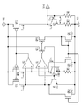
図1には、この発明に係る基準電圧発生回路の一実施例の回路図が示されている。この実施例の基準電圧発生回路は、特に制限されないが、公知の3重ウェル構造を持つCMOS回路が形成される半導体集積回路装置において搭載される。 FIG. 1 is a circuit diagram showing one embodiment of a reference voltage generating circuit according to the present invention. The reference voltage generating circuit of this embodiment is not particularly limited, but is mounted in a semiconductor integrated circuit device in which a known CMOS circuit having a triple well structure is formed.
トランジスタQ1ないしトランジスタQ3は、3重ウェル構造のCMOS回路を利用して形成されるNPN型バイポーラトランジスタである。例えば前記非特許文献1と同様に、P型基板上に形成された深い深さのN型ウェル領域をコレクタとし、上記深い深さのN型ウェル領域に形成されたP型ウェル領域をベースとし、上記P型ウェル領域に形成されたN型領域をエミッタとする縦型構造とされる。
The transistors Q1 to Q3 are NPN bipolar transistors formed using a CMOS circuit having a triple well structure. For example, as in Non-Patent
トランジスタQ3のエミッタ面積を1(×1)とすると、トランジスタQ1のエミッタ面積は、N倍(×N)のように大きく形成される。トランジスタQ1とQ3のベースは、共通に接続される。トランジスタQ3のエミッタは、回路の接地電位(0V)VSSが与えられ、トランジスタQ1のエミッタと基準電位VSSとの間に抵抗R1が設けられる。トランジスタQ1とQ3に流れる電流を同一とし、トランジスタQ1とQ3のエミッタ電流密度差に対応したバンドギャップ電圧(トランジスタQ1とQ3のベース,エミッタ間電圧差)が上記抵抗R1に流れるようにされる。 When the emitter area of the transistor Q3 is 1 (× 1), the emitter area of the transistor Q1 is formed as large as N times (× N). The bases of the transistors Q1 and Q3 are connected in common. The emitter of the transistor Q3 is supplied with the circuit ground potential (0 V) VSS, and a resistor R1 is provided between the emitter of the transistor Q1 and the reference potential VSS. The currents flowing through the transistors Q1 and Q3 are the same, and a band gap voltage (base-emitter voltage difference between the transistors Q1 and Q3) corresponding to the difference between the emitter current densities of the transistors Q1 and Q3 flows through the resistor R1.
上記トランジスタQ1とQ3に同じ電流が流れるようにするために、差動増幅回路A1、A2及びPチャネルMOSFETQP1〜QP3が設けられる。差動増幅回路A1の正相入力(+)と負相入力(−)には、トランジスタQ3のコレクタ電圧とベース電圧が供給される。この差動増幅回路A1の出力電流は、上記トランジスタQ1とQ3のベース電流とされる。これにより、差動増幅回路A1は、上記トランジスタQ3のコレクタとベースとが同電位となるようにトランジスタQ1、Q3のベース電流を形成する。 In order to allow the same current to flow through the transistors Q1 and Q3, differential amplifier circuits A1 and A2 and P-channel MOSFETs QP1 to QP3 are provided. The collector voltage and base voltage of the transistor Q3 are supplied to the positive phase input (+) and the negative phase input (−) of the differential amplifier circuit A1. The output current of the differential amplifier circuit A1 is the base current of the transistors Q1 and Q3. Thereby, the differential amplifier circuit A1 forms the base currents of the transistors Q1 and Q3 so that the collector and base of the transistor Q3 have the same potential.
差動増幅回路A2の正相入力(+)と負相入力(−)には、トランジスタQ1のコレクタ電圧とトランジスタQ1のコレクタ電圧が供給される。この差動増幅回路A2の出力電圧は、PチャネルMOSFETQP1ないしQP3のゲートに供給される。上記PチャネルMOSFETQP1とQP3のドレイン電流は、上記トランジスタQ1とQ3のコレクタに供給される。これにより、差動増幅回路A2とMOSFETQP1,QP3は、上記トランジスタQ1とQ3のコレクタが同電位となるようにMOSFETQP1,QP3のゲート電圧を形成する。MOSFETQP1ないしQP3は、同じサイズに形成されており、上記抵抗R1には上記バンドギャップ電圧に対応した定電流が流れ、これに対応して上記差動増幅回路A1, A2及びPチャネルMOSFETQP1ないしQP3により上記トランジスタQ1とQ3のベース,コレクタ電圧及びコレクタ電流が等しくなるよう設定される。 The collector voltage of the transistor Q1 and the collector voltage of the transistor Q1 are supplied to the positive phase input (+) and the negative phase input (−) of the differential amplifier circuit A2. The output voltage of the differential amplifier circuit A2 is supplied to the gates of the P-channel MOSFETs QP1 to QP3. The drain currents of the P-channel MOSFETs QP1 and QP3 are supplied to the collectors of the transistors Q1 and Q3. As a result, the differential amplifier circuit A2 and the MOSFETs QP1 and QP3 form the gate voltages of the MOSFETs QP1 and QP3 so that the collectors of the transistors Q1 and Q3 have the same potential. The MOSFETs QP1 to QP3 are formed to have the same size, and a constant current corresponding to the band gap voltage flows through the resistor R1, and the differential amplifier circuits A1 and A2 and the P channel MOSFETs QP1 to QP3 correspond to this. The bases, collector voltages and collector currents of the transistors Q1 and Q3 are set to be equal.
この実施例では、特に制限されないが、回路素子数や消費電流の低減のために前記非特許文献1に示された図10の基準電圧発生回路のMOSFETQP4、トランジスタQ4が省略される。図10の回路では、差動増幅回路A1は、トランジスタQ3と同じ構成にされ、コレクタ,ベースが接続されたトランジスタQ4のベース電圧とトランジスタQ1のコレクタ電圧とを受けて両者が等しくなるように動作している。このことに着目し、図1の実施例では、直接的にトランジスタQ1のコレクタ電圧とベース電圧とを差動増幅回路A1に入力することにより、両者が一致させるようトランジスタQ1、Q3のベース電流を形成するものである。
In this embodiment, although not particularly limited, the MOSFET QP4 and the transistor Q4 of the reference voltage generation circuit of FIG. 10 shown in
上記抵抗R1で形成された定電流の温度補償のために、言い換えるならば、出力される基準電圧Vref の温度補償のためにトランジスタQ2、抵抗R2,R3及びPチャネルMOSFETQP2が設けられる。上記トランジスタQ2は、コレクタとベースが接続され、その接続点から基準電圧Vref が出力される。上記トランジスタQ2のエミッタと基準電位VSSとの間には、上記抵抗R2が設けられる。上記トランジスタQ2の接続されたコレクタ,ベースと基準電位VSSとの間に抵抗R3が設けられる。上記トランジスタQ2のコレクタには、上記PチャネルMOSFETQP2のドレイン電流が供給される。上記抵抗R2とR3は、上記基準電圧Vref の温度補償のために、言い換えるならば、基準電圧Vref が温度依存性を持たないような抵抗比に設定される。 A transistor Q2, resistors R2 and R3, and a P-channel MOSFET QP2 are provided for temperature compensation of the constant current formed by the resistor R1, in other words, for temperature compensation of the output reference voltage Vref. The transistor Q2 has a collector and a base connected to each other, and a reference voltage Vref is output from the connection point. The resistor R2 is provided between the emitter of the transistor Q2 and the reference potential VSS. A resistor R3 is provided between the collector and base to which the transistor Q2 is connected and the reference potential VSS. The drain current of the P-channel MOSFET QP2 is supplied to the collector of the transistor Q2. The resistors R2 and R3 are set to a resistance ratio so that the reference voltage Vref does not have temperature dependency in order to compensate the temperature of the reference voltage Vref.
この実施例回路では、上記PチャネルMOSFETQP1〜QP3におけるしきい値電圧のバラツキに対応したオフセット電圧(後述する図4に示すV2〜V4)による基準電圧Vref の変動を抑制するために、ソースと電源電圧VDDとの間に抵抗R4〜R6がそれぞれ設けられる。 In the circuit of this embodiment, in order to suppress the fluctuation of the reference voltage Vref due to the offset voltage (V2 to V4 shown in FIG. 4 described later) corresponding to the variation of the threshold voltage in the P channel MOSFETs QP1 to QP3, Resistors R4 to R6 are respectively provided between the voltage VDD.
図2には、この発明に係る基準電圧発生回路の他の一実施例の回路図が示されている。この実施例は、前記図1と同様な構成にされたトランジスタQ1〜Q3、抵抗R1〜R3、差動増幅回路A1,A2及びPチャネルMOSFETQP1〜QP3を有する基準電圧発生回路において、トランジスタQ1〜Q3における電流増幅率βのバラツキによる基準電圧Vref の変動を抑制するために、PチャネルMOSFETQP5,QP6及びNチャネルMOSFETQN1〜QN3が設けられる。 FIG. 2 is a circuit diagram showing another embodiment of the reference voltage generating circuit according to the present invention. This embodiment is a reference voltage generating circuit having transistors Q1 to Q3, resistors R1 to R3, differential amplifiers A1 and A2 and P channel MOSFETs QP1 to QP3 having the same configuration as that shown in FIG. P channel MOSFETs QP5 and QP6 and N channel MOSFETs QN1 to QN3 are provided to suppress fluctuations in the reference voltage Vref due to variations in the current amplification factor β.
上記PチャネルMOSFETQP5は、ゲートに上記差動増幅回路A1の出力電圧が供給され、ソースには上記電源電圧VDDが印加され、ドレイン電流が上記トランジスタQ1とQ3のベースに供給される。これにより、MOSFETQP5は、上記トランジスタQ1とQ3に流れる合成ベース電流の検出素子として動作する。PチャネルMOSFETQP6は、上記MOSFETQP5と同じサイズにされ、上記PチャネルMOSFETQP5とゲート及びソースが共通接続されることにより、電流ミラー形態にされて同じ電流を流すようにされる。この電流は、基準電位VSS側に設けられたNチャネルMOSFETQN1〜QN3で構成される電流ミラー回路に入力される。 In the P-channel MOSFET QP5, the output voltage of the differential amplifier circuit A1 is supplied to the gate, the power supply voltage VDD is applied to the source, and the drain current is supplied to the bases of the transistors Q1 and Q3. As a result, the MOSFET QP5 operates as a detection element for the combined base current flowing through the transistors Q1 and Q3. The P-channel MOSFET QP6 is the same size as the MOSFET QP5, and the P-channel MOSFET QP5 is connected to the gate and the source in common to form a current mirror so that the same current flows. This current is input to a current mirror circuit composed of N-channel MOSFETs QN1 to QN3 provided on the reference potential VSS side.
つまり、上記PチャネルMOSFETQP6のドレイン電流は、ダイオード接続されたNチャネルMOSFETQN1のドレインに供給される。このNチャネルMOSFETQN1と電流ミラー形態にされたNチャネルMOSFETQN2とQN3は、そのサイズがMOSFETQN1の1/2に設定されて、上記MOSFETQN1の半分の電流を流すようにされる。上記MOSFETQN2のドレインは、上記トランジスタQ1のコレクタに接続される。上記MOSFETQN3のドレインは、上記トランジスタQ3のコレクタに接続される。 That is, the drain current of the P-channel MOSFET QP6 is supplied to the drain of the diode-connected N-channel MOSFET QN1. The N-channel MOSFET QN1 and the N-channel MOSFETs QN2 and QN3 in the form of a current mirror are set to 1/2 the size of the MOSFET QN1 so that half the current of the MOSFET QN1 flows. The drain of the MOSFET QN2 is connected to the collector of the transistor Q1. The drain of the MOSFET QN3 is connected to the collector of the transistor Q3.
図3には、この発明に係る基準電圧発生回路の更に他の一実施例の回路図が示されている。この実施例は、前記図2の基準電圧発生回路において、図1の実施例のようにPチャネルMOSFETQP1〜QP3におけるしきい値電圧のバラツキに対応したオフセット電圧による基準電圧Vref の変動を抑制するために、ソースと電源電圧VDDとの間に抵抗R4〜R6がそれぞれ設けられる。つまり、図1の実施例と図2の実施例を組み合わせて、上記MOSFETQP1〜QP3におけるプロセスバラツキによる基準電圧Vref に対するオフセット電圧の影響と、トランジスタQ1〜Q3における電流増幅率のプロセスバラツキの影響をそれぞれ抑制するというものである。 FIG. 3 is a circuit diagram showing still another embodiment of the reference voltage generating circuit according to the present invention. In this embodiment, in the reference voltage generating circuit of FIG. 2, the fluctuation of the reference voltage Vref due to the offset voltage corresponding to the variation of the threshold voltage in the P-channel MOSFETs QP1 to QP3 as in the embodiment of FIG. 1 is suppressed. In addition, resistors R4 to R6 are provided between the source and the power supply voltage VDD, respectively. That is, by combining the embodiment of FIG. 1 and the embodiment of FIG. 2, the influence of the offset voltage on the reference voltage Vref due to the process variation in the MOSFETs QP1 to QP3 and the influence of the process variation of the current amplification factor in the transistors Q1 to Q3, respectively. It is to suppress.
図4には、この発明を説明するための等価回路図が示されている。同図は、図1の実施例に対応した差動増幅回路における差動素子のプロセスバラツキ、電流ミラーMOSFETQP1〜QP3のプロセスバラツキを検証するためのオフセット電圧V1〜V4が示されている。 FIG. 4 is an equivalent circuit diagram for explaining the present invention. This figure shows offset voltages V1 to V4 for verifying process variations of differential elements and process variations of current mirror MOSFETs QP1 to QP3 in the differential amplifier circuit corresponding to the embodiment of FIG.
図5には、上記オフセット電圧V1〜V4による基準電圧Vref への影響の特性図が示されている。図5は、上記オフセット電圧V1〜V4による基準電圧Vref に対する影響を本願発明者によるコンピュータシミュレーションにより調べたものであり、前記図12と同様に上記各MOSFETQP1〜QP3のしきい値電圧が目標値(0mV)に対してそれぞれ−10mV〜+10mVの範囲で変動したことを想定し、それぞれのオフセット電圧V1〜V4が基準電圧Vref に与える影響を検証したものである。図5からは、基準電圧Vref に最も大きな影響を及ぼす前記MOSFETQP1のしきい値電圧のバラツキ(オフセット電圧V2)においても大幅に抑制されることが判る。 FIG. 5 is a characteristic diagram showing the influence of the offset voltages V1 to V4 on the reference voltage Vref. FIG. 5 shows the influence of the offset voltages V1 to V4 on the reference voltage Vref by a computer simulation by the inventor of the present application. As in FIG. 12, the threshold voltages of the MOSFETs QP1 to QP3 are set to target values ( 0 mV), the influence of each offset voltage V1 to V4 on the reference voltage Vref was verified by assuming that it fluctuated in the range of −10 mV to +10 mV. FIG. 5 shows that the threshold voltage variation (offset voltage V2) of the MOSFET QP1 that has the greatest influence on the reference voltage Vref is also greatly suppressed.
このことを定量的には以下のように説明できる。例えば、図4において、MOSFETQP2について説明すると、ゲート電圧をVGとし、オフセット電圧V3をVOSとし、ソースに設けられた抵抗R5をRのように一般化すると、ドレイン電流をIDSとすると、次式1のように表すことができ、∂IDS/∂VOSを求めると次式2のように表すことができる。他のMOSFETQP1やQP3についてのオフセット電圧V2,V4においても同様である。
This can be explained quantitatively as follows. For example, in FIG. 4, the MOSFET QP2 will be described. When the gate voltage is VG, the offset voltage V3 is VOS, and the resistor R5 provided at the source is generalized as R, the drain current is I DS. 1 can be expressed as follows, and ∂I DS / ∂V OS can be calculated as shown in

上記式2において、∂IDS/∂VOSは、MOSFETのチャネル幅とチャネル長とのサイズ比W/L、オフセット電圧VOSに依存しないで抵抗Rに反比例する式(≒2/R)で表れるものとなる。上記ドレイン電流をIDSは、トランジスタQ2に供給されて基準電圧Vref を形成するので、式2(∂IDS/∂VOS)がオフセット電圧VOSに依存しないことは基準電圧Vref がオフセット電圧VOSのバラツキの影響を受なくできることを意味する。上記抵抗Rの抵抗値がある程度大きくなると、抵抗Rのバラツキの影響も小さくすることができる。この構成では、W/Lを小さくすることができるので低電圧動作に有利な回路となるものである。
In
ちなみに、前記図10の回路のように抵抗が存在しない場合には、ドレイン電流IDSは、ド次式3のように表すことができ、∂IDS/∂VOSを求めると次式4のように表すことができる。この式4かから、電流のオフセット電圧依存性は、サイズ比W/L、オフセット電圧VOSに比例する。サイズ比W/Lを小さくすることは、変動量を小さくすることを意味するが、反面には低電圧動作を困難とするという別の弊害を生じるものである。
Incidentally, when there is no resistance as in the circuit of FIG. 10, the drain current I DS can be expressed by the following equation 3, and ∂I DS / ∂V OS is obtained by the
図6には、前記図2,図3の実施例に対応した上記トランジスタQ1〜Q3の電流増幅率βのプロセスバラツキによる基準電圧Vref への影響の特性図が示されている。図6は、トランジスタQ1〜Q3の電流増幅率の設計値(中心値)βに対して半分(β×0.5)から2倍(β×2)の範囲のような大きなバラツキによる基準電圧Vref に対する影響を本願発明者によるコンピュータシミュレーションにより調べたものである。図6からは、上記基準電圧Vref に対する電流増幅率βのバラツキによる変動幅が大きく抑制されることが判る。 FIG. 6 is a characteristic diagram of the influence on the reference voltage Vref due to process variations of the current amplification factor β of the transistors Q1 to Q3 corresponding to the embodiment of FIGS. FIG. 6 shows the reference voltage Vref due to a large variation in the range of half (β × 0.5) to twice (β × 2) with respect to the design value (center value) β of the current amplification factor of the transistors Q1 to Q3. This is a result of a computer simulation conducted by the inventor of the present application. From FIG. 6, it can be seen that the fluctuation range due to the variation of the current amplification factor β with respect to the reference voltage Vref is greatly suppressed.
このことは、定性的には次のように説明できる。図2において、トランジスタQ1,Q3に供給される電流IOUT には、MOSFETQP5によりトランジスタQ1,Q3のベース電流IB1,IB3を検知し、それをMOSFETQP6−QN1−QN2,QN3を経由して加算される。したがって、トランジスタQ2のコレクタから供給される電流IOUT は、上記トランジスタQ1のコレクタ電流IC1とベース電流IB1に対応したものとなる。したがって、トランジスタQ2のコレクタ電流IC2は上記トランジスタQ1のコレクタ電流IC1に等しく、トランジスタQ2のベース電流IB2は、上記トランジスタQ1のベース電流IB1に等しくできる。これらトランジスタQ1,Q2の電流増幅率βにプロセスバラツキが生じるということは、上記のようにコレクタ側の電流が一定にされるからベース電流IB1やIB2が変化させられるものとなるが、上記の回路ではトランジスタQ1とQ2に流れるコレタク電流及びベース電流が電流増幅率βのバラツキに関係なく同じ条件となり、電流増幅率βがばらついた場合のトランジスタQ2のコレクタ電流の変化量を抑えることができるので、基準電圧Vref の変動を抑えることが出来る。 This can be explained qualitatively as follows. In FIG. 2, the base currents I B1 and I B3 of the transistors Q1 and Q3 are detected by the MOSFET QP5 and added to the current I OUT supplied to the transistors Q1 and Q3 via the MOSFETs QP6-QN1-QN2 and QN3. Is done. Therefore, the current I OUT supplied from the collector of the transistor Q2 corresponds to the collector current I C1 and the base current I B1 of the transistor Q1. Accordingly, the collector current I C2 of the transistor Q2 is equal to the collector current I C1 of the transistor Q1, and the base current I B2 of the transistor Q2 can be equal to the base current I B1 of the transistor Q1. The process variation in the current amplification factor β of these transistors Q1 and Q2 means that the base currents I B1 and I B2 can be changed because the current on the collector side is made constant as described above. In this circuit, the collector current and the base current flowing in the transistors Q1 and Q2 are the same regardless of variations in the current amplification factor β, and the amount of change in the collector current of the transistor Q2 when the current amplification factor β varies can be suppressed. Therefore, fluctuations in the reference voltage Vref can be suppressed.
このことは、定量的には次のように説明できる。例えば、図2において、PチャネルMOSFETQP1〜QP3のドレイン電流をIOUT とし、トランジスタQ1のコレクタ電流をIC1とし、ベース電流をIB1とし、トランジスタQ2のコレクタ電流をIC2とし、ベース電流をIB2とし、ベース,エミッタ間電圧をVBEとし、抵抗R1をR1 とし、抵抗R2をR2 とし、抵抗R3をR3 とすると、ドレイン電流IOUT は、次式5のように表すことができ、基準電圧基準電圧Vref は、次式6のように表すことができる。 This can be explained quantitatively as follows. For example, in FIG. 2, the drain current of P-channel MOSFETs QP1 to QP3 is I OUT , the collector current of transistor Q1 is I C1 , the base current is I B1 , the collector current of transistor Q2 is I C2 , and the base current is I and B2, based, to-emitter voltage and V bE, the resistor R1 and R 1, the resistor R2 and R 2, the resistor R3 and R 3, the drain current I OUT may be expressed by the following equation 5 The reference voltage reference voltage Vref can be expressed as in the following equation (6).
式6において、基準電圧Vref は、電流増幅率βに依存せず、抵抗比R2 /R1 によりVBEの温度依存性をキャンセルさせることができる。
In
ちなみに、図10の基準電圧発生回路においては、PチャネルMOSFETQP2からトランジスタQ2に供給される電流IOUT は、次式7にように表すことができ、基準電圧Vref は次式8のように表すことができる。上記式7及び式8において、いずれも電流増幅率βに依存するものであることが判る。
Incidentally, in the reference voltage generation circuit of FIG. 10, the current I OUT supplied from the P-channel MOSFET QP2 to the transistor Q2 can be expressed by the following equation 7, and the reference voltage Vref is expressed by the
定性的に説明すると、トランジスタQ1は、差動増幅回路A1からベース電流IB1が供給されるので、コレクタ電流IC1がそのままPチャネルMOSFETQP2を通して電流IOUT としてトランジスタQ2のコレクタ側に供給される。しかしながら、トランジスタQ2においては、コレクタとベースが接続されており、上記PチャネルMOSFETQP2から供給される電流IOUT は、トランジスタQ2のコレクタ電流IC2とベース電流IB2のように分配されて流れるものとなる。上記電流IC2とIB2の分配比は、電流増幅率βにより決定されてコレクタ電流IC2が変動することの結果、前記のように基準電圧Vref が変動するものとなる。 To explain qualitatively, since the base current I B1 is supplied from the differential amplifier circuit A1 to the transistor Q1, the collector current I C1 is supplied as it is to the collector side of the transistor Q2 as the current I OUT through the P-channel MOSFET QP2. However, in the transistor Q2, the collector and the base are connected, and the current I OUT supplied from the P-channel MOSFET QP2 is distributed and flows like the collector current I C2 and the base current I B2 of the transistor Q2. Become. The distribution ratio between the currents I C2 and I B2 is determined by the current amplification factor β, and the collector current I C2 varies. As a result, the reference voltage Vref varies as described above.
図7には、この発明の説明図が示されている。図7は、前記図10と図1の基準電圧発生回路におけるPチャネルMOSFETQP1〜QP3のプロセスバラツキで発生するオフセット電圧によるワースト変動量を比較したものであり、図7のAは、前記図10の基準電圧発生回路におけるワースト変動量を示し、基準電圧Vref の変動量が約120mVにもなってしまう。これに対して図7のBは、前記図1の基準電圧回路におけるワースト変動量を示し、基準電圧Vref の変動量が20mV以下に抑制され、前記図10の回路に比べて85%もの改善ができる。 FIG. 7 is an explanatory diagram of the present invention. 7 compares the worst fluctuation amount due to the offset voltage generated by the process variation of the P-channel MOSFETs QP1 to QP3 in the reference voltage generation circuit of FIG. 10 and FIG. 1, and FIG. The worst fluctuation amount in the reference voltage generating circuit is shown, and the fluctuation amount of the reference voltage Vref becomes about 120 mV. On the other hand, FIG. 7B shows the worst fluctuation amount in the reference voltage circuit of FIG. 1, and the fluctuation amount of the reference voltage Vref is suppressed to 20 mV or less, which is an improvement of 85% compared to the circuit of FIG. it can.
図8には、この発明の他の説明図が示されている。図8は、前記図10と図1の基準電圧発生回路における前記トランジスタQ1〜Q3の電流増幅率βのバラツキによるワースト変動量を比較したものであり、図8のAは、前記図10の基準電圧発生回路におけるワースト変動量を示し、基準電圧Vref の変動量が約75mVにもなってしまう。これに対して図8のBは、前記図2の基準電圧回路におけるワースト変動量を示し、基準電圧Vref の変動量が3mV程度に抑制され、前記図10の回路に比べて約97%もの改善ができる。 FIG. 8 shows another explanatory view of the present invention. FIG. 8 is a comparison of worst fluctuation amounts due to variations in the current amplification factors β of the transistors Q1 to Q3 in the reference voltage generation circuit of FIG. 10 and FIG. 1, and FIG. The worst fluctuation amount in the voltage generation circuit is shown, and the fluctuation amount of the reference voltage Vref becomes about 75 mV. On the other hand, FIG. 8B shows the worst fluctuation amount in the reference voltage circuit of FIG. 2, and the fluctuation amount of the reference voltage Vref is suppressed to about 3 mV, which is an improvement of about 97% compared to the circuit of FIG. Can do.
図3の実施例回路では、上記MOSFETQP1〜QP3のオフセット電圧と、トランジスタQ1〜Q3の電流増幅率βのバラツキが上記のように共に改善される。つまり、図10の回路では、MOSFETQP1〜QP3のオフセット電圧のバラツキにより120mV、電流増幅率βのバラツキにより70mVもそれぞれ変動するので、両方で190mVもの基準電圧Vref の変動を考慮しなければならない。これに対して、図3の実施例回路では、両方でも20mV程度にしかならないので、素子のプロセスバラツキの影響を大幅に抑制した基準電圧発生回路を得ることができる。 In the embodiment circuit of FIG. 3, both the offset voltage of the MOSFETs QP1 to QP3 and the variation of the current amplification factor β of the transistors Q1 to Q3 are improved as described above. In other words, in the circuit of FIG. 10, the variation of the offset voltage of MOSFETs QP1 to QP3 varies by 120 mV, and the variation of the current amplification factor β varies by 70 mV. On the other hand, in the embodiment circuit of FIG. 3, since both are only about 20 mV, it is possible to obtain a reference voltage generation circuit in which the influence of the process variation of the elements is greatly suppressed.
図9には、このこの発明に係る基準電圧発生回路の更に他の一実施例の回路図が示されている。この実施例は、前記図3の実施例回路の変形例であり、トランジスタQ1、Q3のベース電流を検知するPチャネルMOSFETQP5と電流ミラー形態にされるPチャネルMOSFETQP6のドレイン電流を直接にトランジスタQ2のコレクタ,ベース接続点に供給するものである。PチャネルMOSFETQP5は、トランジスタQ1とQ3の2個のトランジスタのベース電流を流すので、PチャネルMOSFETQP6のサイズをMOSFETQP5のサイズに比べて1/2にすることにより、前記図3の実施例と同様にトランジスタQ2のコレクタとベース接続点に、上記トランジスタQ1のコレクタ電流IC1とベース電流IB1を供給することができる。これにより、前記図3の実施例と同様にトランジスタQ2のコレクタ電流IC2は上記トランジスタQ1のコレクタ電流IC1に等しく、トランジスタQ2のベース電流IB2は、上記トランジスタQ1のベース電流IB1に等しくできる。 FIG. 9 is a circuit diagram showing still another embodiment of the reference voltage generating circuit according to the present invention. This embodiment is a modification of the embodiment circuit of FIG. 3, and the drain currents of the P-channel MOSFET QP5 for detecting the base currents of the transistors Q1 and Q3 and the P-channel MOSFET QP6 in the form of a current mirror are directly applied to the transistor Q2. It is supplied to the collector and base connection points. Since the P-channel MOSFET QP5 allows the base currents of the two transistors Q1 and Q3 to flow, the size of the P-channel MOSFET QP6 is halved compared to the size of the MOSFET QP5 in the same manner as in the embodiment of FIG. The collector current I C1 and the base current I B1 of the transistor Q1 can be supplied to the collector and base connection point of the transistor Q2. Thus, as in the embodiment of FIG. 3, the collector current I C2 of the transistor Q2 is equal to the collector current I C1 of the transistor Q1, and the base current I B2 of the transistor Q2 is equal to the base current I B1 of the transistor Q1. it can.
この実施例では、PチャネルMOSFETQP5,QP6が前記MOSFETQP1〜QP3と同様な回路構成とされることから、PチャネルMOSFETQP5,QP6におけるオフセット電圧が基準電圧Vref に影響を及ぼすものと考えられる。したがって、これを抑制するためにPチャネルMOSFETQP5,QP6のソース側にも前記PチャネルMOSFETQP1〜QP3のソース側に設けられた抵抗R4〜R6と同様な抵抗R7とR8が設けられる。この実施例は、前記図3の実施例と比較して電流パスが減り、低消費電力化、小面積化につながる。 In this embodiment, since the P channel MOSFETs QP5 and QP6 have the same circuit configuration as the MOSFETs QP1 to QP3, the offset voltage in the P channel MOSFETs QP5 and QP6 is considered to affect the reference voltage Vref. Therefore, in order to suppress this, resistors R7 and R8 similar to the resistors R4 to R6 provided on the source side of the P channel MOSFETs QP1 to QP3 are also provided on the source side of the P channel MOSFETs QP5 and QP6. In this embodiment, the number of current paths is reduced as compared with the embodiment of FIG. 3, leading to low power consumption and a small area.
上記基準電圧発生回路を形成される半導体集積回路装置は、CMOS回路で構成されるものが好適である。この場合、素子のプロセスバラツキに影響されない回路とすることができることから、SOC搭載メモリやマイクロプロセッサに有効なものとなる。これらの半導体集積回路装置は、低電圧化のニーズが高く、しかも高精度な基準電圧が必要であるからである。また、プロセスにより異なるβに対応した再設計が不要になることから、ハードウェアIP(Intellectual Propety) コアに利用して有効な技術となる。更に、プロセッサ等トリミングすることが難しい製品では、MOSFETのしきい値電圧や電流増幅率βのバラツキによる基準電圧の変動量が小さいので、トリミング回路を準備しておく必要が無いことから有効である。 The semiconductor integrated circuit device on which the reference voltage generating circuit is formed is preferably composed of a CMOS circuit. In this case, since it is possible to make the circuit unaffected by the process variation of the element, the circuit is effective for the SOC mounted memory and the microprocessor. This is because these semiconductor integrated circuit devices have a high need for a low voltage and require a highly accurate reference voltage. In addition, since redesign corresponding to different β is not required depending on the process, it becomes an effective technology when used for a hardware IP (Intellectual Propety) core. Furthermore, products that are difficult to trim, such as processors, are effective because the amount of variation in the reference voltage due to variations in the MOSFET threshold voltage and current amplification factor β is small, and it is not necessary to prepare a trimming circuit. .
以上本発明者によってなされた発明を、前記実施形態に基づき具体的に説明したが、本発明は、前記実施形態に限定されるものではなく、その要旨を逸脱しない範囲において種々変更可能である。例えば、トランジスタQ1〜Q3は、前記のような3重ウェル構造のCMOSプロセスで形成される半導体領域で構成されるものの他、ラテラル構造のバイポーラトランジスタを用いるもの等種々の変形を採ることができる。負電圧を電源電圧とした場合には、トランジスタやMOSFETの導電型を逆にすればよい。上記抵抗R4〜R8等は、前記のように比較的高い抵抗値にされる必要があるので、ポリシリコン抵抗等を利用することができる。 Although the invention made by the inventor has been specifically described based on the above embodiment, the present invention is not limited to the above embodiment, and various modifications can be made without departing from the scope of the invention. For example, the transistors Q1 to Q3 can be variously modified such as a transistor using a lateral structure bipolar transistor in addition to a semiconductor region formed by a CMOS process having a triple well structure as described above. When the negative voltage is used as the power supply voltage, the conductivity type of the transistor or MOSFET may be reversed. Since the resistors R4 to R8 and the like need to have relatively high resistance values as described above, a polysilicon resistor or the like can be used.
この発明は、MOSFETで構成される半導体集積回路装置に搭載される基準電圧発生回路として広く利用でき、低電圧化のニーズが高く、しかも高精度な基準電圧を必要とするSOC搭載メモリやマイクロプロセッサ、ハードウェアIPコア製品、トリミングすることが難しい各種半導体集積回路装置等に利用して有効なものとなる。 The present invention can be widely used as a reference voltage generating circuit mounted on a semiconductor integrated circuit device composed of MOSFETs, has a high need for lowering the voltage, and also requires a highly accurate reference voltage and a microprocessor mounted with an SOC. It is effective for use in hardware IP core products, various semiconductor integrated circuit devices that are difficult to trim.
A1,A2…差動増幅回路、Q1〜Q4…トランジスタ、QP1〜QP6…PチャネルMOSFET、QN1〜QN3…NチャネルMOSFET、R1〜R8…抵抗、 A1, A2 ... differential amplifier circuit, Q1-Q4 ... transistor, QP1-QP6 ... P-channel MOSFET, QN1-QN3 ... N-channel MOSFET, R1-R8 ... resistor,
Claims (10)
上記参照基準電圧発生回路は、
エミッタが基準電位に接続された第1バイポーラトランジスタと、
上記第1バイポーラトランジスタのエミッタ面積よりも大きなエミッタ面積を有し、エミッタが第1抵抗素子を介して上記基準電位に接続され、ベースが上記第1バイポーラトランジスタのベースに接続された第2バイポーラトランジスタと、
上記第1バイポーラトランジスタのコレクタ電圧とベース電圧を一対の入力とし、出力信号を上記第1及び第2バイポーラトランジスタのベースに帰還伝達する構成によって上記第1バイポーラトランジスタのベース電圧とコレクタ電圧が等しくなる状態を維持する第1差動増幅回路と、
コレクタとベースとが結合され、エミッタと上記基準電位との間に第2抵抗素子が設けられ、上記結合されたコレクタ・ベースと上記基準電位との間に第3抵抗素子が設けられた第3バイポーラトランジスタと、
上記第1バイポーラトランジスタのコレクタ電圧と第2バイポーラトランジスタのコレクタの電圧を一対の入力とする第2差動増幅回路と、
上記第2差動増幅回路の出力電圧がゲートに供給され、ソースが第4ないし第6抵抗素子を介してそれぞれ電源電位に接続され、上記第1ないし第3バイポーラトランジスタのコレクタ電流をそれぞれ形成する第1ないし第3MOSFETと
を有し、
参照基準電圧が上記第3バイポーラトランジスタの結合されたコレクタ・ベースから出力され、
上記第1抵抗素子は、エミッタ面積の異なる上記第1バイポーラトランジスタと上記第2バイポーラトランジスタとの間に生じるエミッタ電流密度の違いに対応して発生するエミッタ・ベース間電圧の差分を補償する大きさの抵抗値に設定され、
上記第1抵抗素子と第2抵抗素子は、上記参照基準電圧に生じる温度依存性を相殺する抵抗比に設定され、
上記第4ないし第6抵抗素子は、上記第1ないし第3MOSFETを含む電流路間に生じるバラツキに起因する上記参照基準電圧の変動を抑制する大きさの抵抗値に設定されてなる
半導体集積回路装置。 A semiconductor integrated circuit device which have a reference standard voltage generation circuit formed by circuit elements including a bipolar transistor and a MOSFET formed by CMOS manufacturing processes,
The reference reference voltage generation circuit is
A first bipolar transistor having an emitter connected to a reference potential ;
It has a larger emitter area than the emitter area of the first bipolar transistor, an emitter connected to the reference potential via a first resistor element, a second bipolar transistor having a base connected to the base of the first bipolar transistor When,
The base voltage and collector voltage of the first bipolar transistor are equalized by a configuration in which the collector voltage and base voltage of the first bipolar transistor are used as a pair of inputs and the output signal is fed back to the bases of the first and second bipolar transistors. A first differential amplifier circuit for maintaining the state ;
A collector and a base are coupled, a second resistance element is provided between the emitter and the reference potential, and a third resistance element is provided between the coupled collector and base and the reference potential. A bipolar transistor;
A second differential amplifier circuit having a pair of inputs, the collector voltage of the first bipolar transistor and the collector voltage of the second bipolar transistor;
The output voltage of the second differential amplifier circuit is supplied to the gate, the source is connected to the power supply potential via the fourth to sixth resistance elements, and forms the collector current of the first to third bipolar transistors, respectively. First to third MOSFETs, and
A reference reference voltage is output from the combined collector and base of the third bipolar transistor;
The first resistance element is sized to compensate for a difference in emitter-base voltage generated corresponding to a difference in emitter current density generated between the first bipolar transistor and the second bipolar transistor having different emitter areas. Is set to the resistance value of
The first resistance element and the second resistance element are set to a resistance ratio that cancels the temperature dependence occurring in the reference standard voltage,
The semiconductor integrated circuit device in which the fourth to sixth resistance elements are set to a resistance value large enough to suppress variations in the reference reference voltage caused by variations occurring between current paths including the first to third MOSFETs. .
ソースが上記電源電位に接続され、ゲートが上記第1差動増幅回路の出力に接続され、ドレインが上記第1及び第2バイポーラトランジスタのベースに共通接続され、上記第1差動増幅回路の上記出力信号で制御されるドレイン電流を上記共通結合されたベースに帰還伝達する構成に接続された第4MOSFETと、The source is connected to the power supply potential, the gate is connected to the output of the first differential amplifier circuit, the drain is commonly connected to the bases of the first and second bipolar transistors, and the first differential amplifier circuit A fourth MOSFET connected in a configuration that feeds back a drain current controlled by an output signal to the commonly coupled base;
上記第4MOSFETで検出された上記第1及び第2バイポーラトランジスタのベース電流に対応して、上記第3バイポーラトランジスタの上記コレクタ・ベース結合部に供給される電流の変動を抑制する電流ミラー回路と、を更に有するA current mirror circuit that suppresses fluctuations in the current supplied to the collector-base coupling portion of the third bipolar transistor in response to the base currents of the first and second bipolar transistors detected by the fourth MOSFET; Further
半導体集積回路装置。Semiconductor integrated circuit device.
上記参照基準電圧発生回路は、
エミッタが基準電位に接続された第1バイポーラトランジスタと、
上記第1バイポーラトランジスタのエミッタ面積よりもエミッタ面積が大きく形成され、エミッタが第1抵抗素子を介して上記基準電位に接続され、ベースが上記第1バイポーラトランジスタのベースに接続された第2バイポーラトランジスタと、
上記第1バイポーラトランジスタのコレクタ電圧とベース電圧を一対の入力とし、出力信号を上記第1及び第2バイポーラトランジスタのベースに帰還伝達する構成によって上記第1バイポーラトランジスタのベース電圧とコレクタ電圧が等しくなる状態を維持する第1差動増幅回路と、
コレクタとベースとが結合され、エミッタと上記基準電位との間に第2抵抗素子が設けられ、上記結合されたコレクタ・ベースと上記基準電位との間に第3抵抗素子が設けられた第3バイポーラトランジスタと、
上記第1バイポーラトランジスタのコレクタ電圧と上記第2バイポーラトランジスタのコレクタ電圧を一対の入力とする第2差動増幅回路と、
上記第2差動増幅回路の出力電圧がゲートに共通に供給され、ソースがそれぞれ電源電位に接続され、上記第1ないし第3バイポーラトランジスタのコレクタに供給される電流が等しくなるような電流をそれぞれ形成する第1ないし第3MOSFETと
を有し、
参照基準電圧が上記第3バイポーラトランジスタの結合されたコレクタ・ベースから出力され、
上記第1抵抗素子は、エミッタ面積の異なる上記第1バイポーラトランジスタと上記第2バイポーラトランジスタとの間に生じるエミッタ電流密度の違いに対応して発生するエミッタ・ベース間電圧の差分を補償する大きさの抵抗値に設定され、
上記第1抵抗素子と第2抵抗素子は、上記参照基準電圧に生じる温度依存性を相殺する抵抗比に設定されてなり、
ソースが上記電源電位に接続され、ドレインが上記第1及び第2バイポーラトランジスタのベースに接続され、上記第1差動増幅回路の出力電圧がゲートに供給された第4MOSFETと、
上記第4MOSFETで検出された上記第1及び第2バイポーラトランジスタのベース電流に対応して、上記第3バイポーラトランジスタの上記コレクタ・ベース結合部に供給される電流の変動を抑制する電流ミラー回路と、を更に有する
半導体集積回路装置。 A semiconductor integrated circuit device which have a reference standard voltage generation circuit formed by circuit elements including a bipolar transistor and a MOSFET formed by CMOS manufacturing processes,
The reference reference voltage generation circuit is
A first bipolar transistor having an emitter connected to a reference potential ;
A second bipolar transistor having an emitter area larger than that of the first bipolar transistor, an emitter connected to the reference potential via a first resistance element, and a base connected to the base of the first bipolar transistor When,
The base voltage and collector voltage of the first bipolar transistor are equalized by a configuration in which the collector voltage and base voltage of the first bipolar transistor are used as a pair of inputs and the output signal is fed back to the bases of the first and second bipolar transistors. A first differential amplifier circuit for maintaining the state ;
A collector and a base are coupled, a second resistance element is provided between the emitter and the reference potential, and a third resistance element is provided between the coupled collector and base and the reference potential. A bipolar transistor;
A second differential amplifier circuit for the collector voltage and collector voltage of the second bipolar transistor of said first bipolar transistor with a pair of inputs,
The output voltage of the second differential amplifier circuit is commonly supplied to the gate, the source is connected to the power supply potential, and the currents supplied to the collectors of the first to third bipolar transistors are equal. First to third MOSFETs to be formed;
A reference reference voltage is output from the combined collector and base of the third bipolar transistor;
The first resistance element is sized to compensate for a difference in emitter-base voltage generated corresponding to a difference in emitter current density generated between the first bipolar transistor and the second bipolar transistor having different emitter areas. Is set to the resistance value of
It said first resistive element and the second resistive element is made is set to a resistance ratio to offset the temperature dependence caused to the reference standard voltage,
Source connected to the power supply potential, a drain connected to the base of said first and second bipolar transistors, a first 4MOSFET the output voltage of the first differential amplifier circuit is supplied to the gate,
In response to the base current of the detected said first and second bipolar transistors in said first 4MOSFET, a current mirror circuit that to suppress the fluctuation of the current supplied to the collector-base junction of the third bipolar transistor the semiconductor integrated circuit device further comprising a.
上記第1乃至第3MOSFETのソースが第4乃至第6抵抗素子を介してそれぞれ電源電位に接続され、上記第4乃至第6抵抗素子は、上記製造プロセスに起因して上記第1乃至第3MOSFETの間に生じるしきい値電圧のバラツキを抑制する大きさの抵抗値に設定されてなるThe sources of the first to third MOSFETs are connected to the power supply potential via the fourth to sixth resistance elements, respectively, and the fourth to sixth resistance elements are connected to the first to third MOSFETs due to the manufacturing process. The resistance value is set to a magnitude that suppresses variations in threshold voltage that occur between them.
半導体集積回路装置。Semiconductor integrated circuit device.
上記CMOS製造プロセスは、P型基板上にN型ウェル領域を形成する段階と、上記N型ウェル領域内にP型ウェル領域を形成する段階と、上記P型ウェル領域内にNチャネルMOSFETのソース,ドレインを形成するためのN型領域を形成する段階とを含み、The CMOS manufacturing process includes a step of forming an N-type well region on a P-type substrate, a step of forming a P-type well region in the N-type well region, and a source of an N-channel MOSFET in the P-type well region. Forming an N-type region for forming a drain,
上記第1ないし第3バイポーラトランジスタは、上記N型ウェル領域を形成する段階で形成されたN型ウェル領域をコレクタとし、上記P型ウェル領域を形成する段階で上記N型コレクタ領域内に形成されるP型領域をベースとし、上記ソース,ドレインを形成するためのN型領域を形成する段階で上記P型ベース領域に形成されたN型領域をエミッタとするものであり、The first to third bipolar transistors are formed in the N-type collector region in the step of forming the P-type well region, using the N-type well region formed in the step of forming the N-type well region as a collector. The N-type region formed in the P-type base region at the stage of forming the N-type region for forming the source and drain is used as the emitter.
上記第1ないし第3MOSFETはそれぞれ、上記N型ウェル領域上に形成されたP型領域をソース,ドレインとするPチャネルMOSFETであるEach of the first to third MOSFETs is a P-channel MOSFET having a P-type region formed on the N-type well region as a source and a drain.
半導体集積回路装置。Semiconductor integrated circuit device.
上記電流ミラー回路は、
上記第4MOSFETと、
ソースが上記電源電位に接続され、ゲートが上記第4MOSFETのゲートに共通接続され、第4MOSFETに流れる電流に対し同じ電流を流すように電流ミラー形態に接続された第5MOSFETと、
上記第5MOSFETのドレインと上記基準電位の間に接続された第6MOSFETと、
上記第2バイポーラトランジスタと第1抵抗素子で構成される電流路に対し並列接続された第7MOSFETと、
上記第1バイポーラトランジスタの電流路に対し並列接続された第8MOSFETと
を含み、
上記第6ないし第8MOSFETのゲートを上記第5MOSFETのドレインに共通接続し、上記第7及び第8MOSFETを上記第6MOSFETに対しそれぞれ半分の電流を流す電流ミラー形態に接続して構成されたものである
半導体集積回路装置。 In any of claims 2 to 4 ,
The current mirror circuit is
The fourth MOSFET ;
A fifth MOSFET having a source connected to the power supply potential, a gate commonly connected to the gate of the fourth MOSFET , and a current mirror configured to cause the same current to flow through the fourth MOSFET;
A sixth MOSFET connected between the drain of the fifth MOSFET and the reference potential;
A seventh MOSFET connected in parallel to the current path composed of the second bipolar transistor and the first resistance element;
An eighth MOSFET connected in parallel to the current path of the first bipolar transistor;
Including
The gate of the upper Symbol sixth to 8MOSFET commonly connected to a drain of the first 5MOSFET, those of the seventh and 8MOSFET configured by connecting a current mirror configuration to flow a current of each half to the second 6MOSFET A semiconductor integrated circuit device.
上記電流ミラー回路は、
上記第4MOSFETと、
ソースが上記電源電位に接続され、ゲートが上記第4MOSFETのゲートに共通接続され、第4MOSFETに対し半分のサイズに形成され、ドレイン電流を電流ミラー形態で上記第3バイポーラトランジスタのコレクタ・ベース結合部に供給する第5MOSFETとを有する
半導体集積回路装置。 In any of claims 2 to 4 ,
The current mirror circuit is
The fourth MOSFET ;
Source connected to the power supply potential, a gate is commonly connected to a gate of the first 4MOSFET, formed half the size with respect to the 4MOSFET, the collector-base junction of the third bipolar transistor and the drain current in a current mirror configuration the semiconductor integrated circuit device for chromatic and first 5MOSFET supplied to.
上記第4及び第5MOSFETのソースはそれぞれ第7及び第8抵抗素子を介して上記電源電位に接続されているThe sources of the fourth and fifth MOSFETs are connected to the power supply potential via seventh and eighth resistance elements, respectively.
半導体集積回路装置。Semiconductor integrated circuit device.
上記電流ミラー回路は、The current mirror circuit is
上記第4MOSFETと、The fourth MOSFET;
ソースが上記電源電位に接続され、ゲートが上記第4MOSFETのゲートに共通接続され、第4MOSFETと同じサイズに形成され、ドレイン電流を電流ミラー形態で供給する第5MOSFETと、A fifth MOSFET having a source connected to the power supply potential, a gate commonly connected to the gate of the fourth MOSFET, the same size as the fourth MOSFET, and supplying a drain current in the form of a current mirror;
上記第5MOSFETのドレインと上記基準電位の間に接続された第6MOSFETと、A sixth MOSFET connected between the drain of the fifth MOSFET and the reference potential;
上記第2バイポーラトランジスタと第1抵抗素子で構成される電流路に対し並列接続された第7MOSFETと、A seventh MOSFET connected in parallel to the current path composed of the second bipolar transistor and the first resistance element;
上記第1バイポーラトランジスタの電流路に対し並列接続された第8MOSFETとAn eighth MOSFET connected in parallel to the current path of the first bipolar transistor;
を有し、Have
上記第6乃至第8MOSFETのゲートを上記第5MOSFETのドレインに共通接続し、上記第7及び第8MOSFETを上記第6MOSFETに対し電流ミラー形態に接続して構成されたものであるThe gates of the sixth to eighth MOSFETs are commonly connected to the drain of the fifth MOSFET, and the seventh and eighth MOSFETs are connected to the sixth MOSFET in a current mirror configuration.
半導体集積回路装置。Semiconductor integrated circuit device.
上記CMOS製造プロセスは、P型基板上にN型ウェル領域を形成する段階と、上記N型ウェル領域内にP型ウェル領域を形成する段階と、上記P型ウェル領域内にNチャネルMOSFETのソース,ドレインを形成するためのN型領域を形成する段階とを含み、
上記第1ないし第3バイポーラトランジスタは、上記N型ウェル領域を形成する段階で形成されたN型ウェル領域をコレクタとし、上記P型ウェル領域を形成する段階で上記N型コレクタ領域内に形成されるP型領域をベースとし、上記ソース,ドレインを形成するためのN型領域を形成する段階でP型ベース領域内に形成されたN型領域をエミッタとするものであり、
上記第1ないし第5MOSFETは、上記N型ウェル領域上に形成されたP型のソース,ドレインが形成されたPチャネルMOSFETである
半導体集積回路装置。 In any of claims 6 to 9,
The CMOS manufacturing process includes a step of forming an N-type well region on a P-type substrate, a step of forming a P-type well region in the N-type well region, and a source of an N-channel MOSFET in the P-type well region. Forming an N-type region for forming a drain,
The first to third bipolar transistor, the N-type well region formed at the stage of forming the upper Symbol N-type well region and a collector, formed on the N-type collector region at the stage of forming the P-type well region the P-type region as a base to be, is intended to be the source, the emitter of the N-type region formed in P-type base region at the stage of forming the N-type region for forming the drain,
The first to 5MOSFET The semiconductor integrated circuit device is a P-channel MOSFET in which the N-type well region P-type source formed on, the drain is formed.
Priority Applications (1)
| Application Number | Priority Date | Filing Date | Title |
|---|---|---|---|
| JP2008114930A JP5175131B2 (en) | 2008-04-25 | 2008-04-25 | Semiconductor integrated circuit device |
Applications Claiming Priority (1)
| Application Number | Priority Date | Filing Date | Title |
|---|---|---|---|
| JP2008114930A JP5175131B2 (en) | 2008-04-25 | 2008-04-25 | Semiconductor integrated circuit device |
Publications (3)
| Publication Number | Publication Date |
|---|---|
| JP2009265954A JP2009265954A (en) | 2009-11-12 |
| JP2009265954A5 JP2009265954A5 (en) | 2011-05-26 |
| JP5175131B2 true JP5175131B2 (en) | 2013-04-03 |
Family
ID=41391728
Family Applications (1)
| Application Number | Title | Priority Date | Filing Date |
|---|---|---|---|
| JP2008114930A Active JP5175131B2 (en) | 2008-04-25 | 2008-04-25 | Semiconductor integrated circuit device |
Country Status (1)
| Country | Link |
|---|---|
| JP (1) | JP5175131B2 (en) |
Families Citing this family (2)
| Publication number | Priority date | Publication date | Assignee | Title |
|---|---|---|---|---|
| CN107990992B (en) * | 2017-11-27 | 2019-10-11 | 电子科技大学 | Temperature sensors of high precision and precision adjusting method |
| CN110716605B (en) * | 2019-10-14 | 2020-11-17 | 西安理工大学 | Quick start PTAT current source based on operational amplifier positive feedback mechanism |
Family Cites Families (6)
| Publication number | Priority date | Publication date | Assignee | Title |
|---|---|---|---|---|
| JPS63175907A (en) * | 1987-01-16 | 1988-07-20 | Mitsubishi Electric Corp | Constant-current circuit |
| JP3106078B2 (en) * | 1994-12-28 | 2000-11-06 | シャープ株式会社 | LCD drive power supply |
| JP2001085548A (en) * | 1999-09-09 | 2001-03-30 | Sony Corp | BiCMOS ELEMENT, OPERATIONAL AMPLFIER, AND BGR CIRCUIT |
| JP2004310444A (en) * | 2003-04-07 | 2004-11-04 | Nippon Telegr & Teleph Corp <Ntt> | Voltage generating circuit |
| JP2005130020A (en) * | 2003-10-21 | 2005-05-19 | Toshiba Corp | Analog level shifter |
| JP2007287095A (en) * | 2006-04-20 | 2007-11-01 | Nec Electronics Corp | Reference voltage generating circuit |
-
2008
- 2008-04-25 JP JP2008114930A patent/JP5175131B2/en active Active
Also Published As
| Publication number | Publication date |
|---|---|
| JP2009265954A (en) | 2009-11-12 |
Similar Documents
| Publication | Publication Date | Title |
|---|---|---|
| US7495505B2 (en) | Low supply voltage band-gap reference circuit and negative temperature coefficient current generation unit thereof and method for supplying band-gap reference current | |
| JP4817825B2 (en) | Reference voltage generator | |
| US7323857B2 (en) | Current source with adjustable temperature coefficient | |
| US7411442B2 (en) | Constant current circuit operating independent of temperature | |
| US10152079B2 (en) | Circuit arrangement for the generation of a bandgap reference voltage | |
| TWI418968B (en) | Circuit and method for generating reference voltage and reference current | |
| JP3519361B2 (en) | Bandgap reference circuit | |
| US20210356983A1 (en) | System and method for voltage generation | |
| Fayomi et al. | Sub 1 V CMOS bandgap reference design techniques: a survey | |
| KR20020053188A (en) | Current mirror type bandgap reference voltage generator | |
| GB2425419A (en) | An overtemperature detector for integrated circuits, using hysteresis | |
| US20090051342A1 (en) | Bandgap reference circuit | |
| JP2008108009A (en) | Reference voltage generation circuit | |
| JP2006262348A (en) | Semiconductor circuit | |
| US9246479B2 (en) | Low-offset bandgap circuit and offset-cancelling circuit therein | |
| WO2009118267A1 (en) | A bias current generator | |
| JP2010176258A (en) | Voltage generation circuit | |
| US10379567B2 (en) | Bandgap reference circuitry | |
| JP4084872B2 (en) | Voltage regulator | |
| JP5175131B2 (en) | Semiconductor integrated circuit device | |
| JP2007287095A (en) | Reference voltage generating circuit | |
| US20130063201A1 (en) | Reference voltage circuit | |
| JP4263056B2 (en) | Reference voltage generator | |
| JP2005044051A (en) | Reference voltage generating circuit | |
| JP5707634B2 (en) | Tunnel current circuit |
Legal Events
| Date | Code | Title | Description |
|---|---|---|---|
| A521 | Written amendment |
Free format text: JAPANESE INTERMEDIATE CODE: A523 Effective date: 20110413 |
|
| A621 | Written request for application examination |
Free format text: JAPANESE INTERMEDIATE CODE: A621 Effective date: 20110413 |
|
| A977 | Report on retrieval |
Free format text: JAPANESE INTERMEDIATE CODE: A971007 Effective date: 20121206 |
|
| TRDD | Decision of grant or rejection written | ||
| A01 | Written decision to grant a patent or to grant a registration (utility model) |
Free format text: JAPANESE INTERMEDIATE CODE: A01 Effective date: 20121212 |
|
| A61 | First payment of annual fees (during grant procedure) |
Free format text: JAPANESE INTERMEDIATE CODE: A61 Effective date: 20130104 |
|
| R150 | Certificate of patent or registration of utility model |
Ref document number: 5175131 Country of ref document: JP Free format text: JAPANESE INTERMEDIATE CODE: R150 |
|
| S531 | Written request for registration of change of domicile |
Free format text: JAPANESE INTERMEDIATE CODE: R313531 |
|
| R350 | Written notification of registration of transfer |
Free format text: JAPANESE INTERMEDIATE CODE: R350 |
|
| S111 | Request for change of ownership or part of ownership |
Free format text: JAPANESE INTERMEDIATE CODE: R313113 |
|
| R350 | Written notification of registration of transfer |
Free format text: JAPANESE INTERMEDIATE CODE: R350 |