JP7077320B2 - コリメートされたledの光照射野ディスプレイ - Google Patents
コリメートされたledの光照射野ディスプレイ Download PDFInfo
- Publication number
- JP7077320B2 JP7077320B2 JP2019530717A JP2019530717A JP7077320B2 JP 7077320 B2 JP7077320 B2 JP 7077320B2 JP 2019530717 A JP2019530717 A JP 2019530717A JP 2019530717 A JP2019530717 A JP 2019530717A JP 7077320 B2 JP7077320 B2 JP 7077320B2
- Authority
- JP
- Japan
- Prior art keywords
- light
- micro led
- field display
- layer
- microlenses
- Prior art date
- Legal status (The legal status is an assumption and is not a legal conclusion. Google has not performed a legal analysis and makes no representation as to the accuracy of the status listed.)
- Active
Links
- 239000000758 substrate Substances 0.000 claims description 14
- 238000003491 array Methods 0.000 claims description 9
- 230000003287 optical effect Effects 0.000 claims description 9
- 239000003086 colorant Substances 0.000 claims description 3
- 239000010410 layer Substances 0.000 description 81
- 238000000034 method Methods 0.000 description 24
- 239000000463 material Substances 0.000 description 9
- 238000001459 lithography Methods 0.000 description 8
- 230000005540 biological transmission Effects 0.000 description 6
- 239000011347 resin Substances 0.000 description 5
- 229920005989 resin Polymers 0.000 description 5
- XLOMVQKBTHCTTD-UHFFFAOYSA-N Zinc monoxide Chemical compound [Zn]=O XLOMVQKBTHCTTD-UHFFFAOYSA-N 0.000 description 4
- 230000015572 biosynthetic process Effects 0.000 description 3
- 238000010586 diagram Methods 0.000 description 3
- 238000010292 electrical insulation Methods 0.000 description 3
- 238000004519 manufacturing process Methods 0.000 description 3
- 229910052751 metal Inorganic materials 0.000 description 3
- 239000002184 metal Substances 0.000 description 3
- 229910052594 sapphire Inorganic materials 0.000 description 3
- 239000010980 sapphire Substances 0.000 description 3
- 229910001218 Gallium arsenide Inorganic materials 0.000 description 2
- GWEVSGVZZGPLCZ-UHFFFAOYSA-N Titan oxide Chemical compound O=[Ti]=O GWEVSGVZZGPLCZ-UHFFFAOYSA-N 0.000 description 2
- 239000000853 adhesive Substances 0.000 description 2
- 230000001070 adhesive effect Effects 0.000 description 2
- 238000000151 deposition Methods 0.000 description 2
- 229910003460 diamond Inorganic materials 0.000 description 2
- 239000010432 diamond Substances 0.000 description 2
- 230000005670 electromagnetic radiation Effects 0.000 description 2
- 238000005530 etching Methods 0.000 description 2
- 210000003128 head Anatomy 0.000 description 2
- 238000001020 plasma etching Methods 0.000 description 2
- 230000000007 visual effect Effects 0.000 description 2
- 239000011787 zinc oxide Substances 0.000 description 2
- GYHNNYVSQQEPJS-UHFFFAOYSA-N Gallium Chemical compound [Ga] GYHNNYVSQQEPJS-UHFFFAOYSA-N 0.000 description 1
- 229910052581 Si3N4 Inorganic materials 0.000 description 1
- VYPSYNLAJGMNEJ-UHFFFAOYSA-N Silicium dioxide Chemical compound O=[Si]=O VYPSYNLAJGMNEJ-UHFFFAOYSA-N 0.000 description 1
- HCHKCACWOHOZIP-UHFFFAOYSA-N Zinc Chemical compound [Zn] HCHKCACWOHOZIP-UHFFFAOYSA-N 0.000 description 1
- 239000012790 adhesive layer Substances 0.000 description 1
- 210000004556 brain Anatomy 0.000 description 1
- 238000005056 compaction Methods 0.000 description 1
- 239000003989 dielectric material Substances 0.000 description 1
- 239000002019 doping agent Substances 0.000 description 1
- 238000001312 dry etching Methods 0.000 description 1
- 230000005611 electricity Effects 0.000 description 1
- 230000004424 eye movement Effects 0.000 description 1
- 229910052733 gallium Inorganic materials 0.000 description 1
- 239000011521 glass Substances 0.000 description 1
- 230000004886 head movement Effects 0.000 description 1
- 229910052738 indium Inorganic materials 0.000 description 1
- APFVFJFRJDLVQX-UHFFFAOYSA-N indium atom Chemical compound [In] APFVFJFRJDLVQX-UHFFFAOYSA-N 0.000 description 1
- AMGQUBHHOARCQH-UHFFFAOYSA-N indium;oxotin Chemical compound [In].[Sn]=O AMGQUBHHOARCQH-UHFFFAOYSA-N 0.000 description 1
- 238000009616 inductively coupled plasma Methods 0.000 description 1
- 238000010884 ion-beam technique Methods 0.000 description 1
- 238000003801 milling Methods 0.000 description 1
- 239000000203 mixture Substances 0.000 description 1
- 230000003647 oxidation Effects 0.000 description 1
- 238000007254 oxidation reaction Methods 0.000 description 1
- 230000008447 perception Effects 0.000 description 1
- 238000000206 photolithography Methods 0.000 description 1
- 238000009832 plasma treatment Methods 0.000 description 1
- 238000005498 polishing Methods 0.000 description 1
- 238000003825 pressing Methods 0.000 description 1
- 230000005855 radiation Effects 0.000 description 1
- HBMJWWWQQXIZIP-UHFFFAOYSA-N silicon carbide Chemical compound [Si+]#[C-] HBMJWWWQQXIZIP-UHFFFAOYSA-N 0.000 description 1
- 229910010271 silicon carbide Inorganic materials 0.000 description 1
- HQVNEWCFYHHQES-UHFFFAOYSA-N silicon nitride Chemical compound N12[Si]34N5[Si]62N3[Si]51N64 HQVNEWCFYHHQES-UHFFFAOYSA-N 0.000 description 1
- 229910052814 silicon oxide Inorganic materials 0.000 description 1
- 239000002904 solvent Substances 0.000 description 1
- 239000000126 substance Substances 0.000 description 1
- 239000004408 titanium dioxide Substances 0.000 description 1
- XLYOFNOQVPJJNP-UHFFFAOYSA-N water Substances O XLYOFNOQVPJJNP-UHFFFAOYSA-N 0.000 description 1
- 238000001039 wet etching Methods 0.000 description 1
- 229910052725 zinc Inorganic materials 0.000 description 1
- 239000011701 zinc Substances 0.000 description 1
Images


Classifications
-
- G—PHYSICS
- G02—OPTICS
- G02B—OPTICAL ELEMENTS, SYSTEMS OR APPARATUS
- G02B27/00—Optical systems or apparatus not provided for by any of the groups G02B1/00 - G02B26/00, G02B30/00
- G02B27/02—Viewing or reading apparatus
-
- H—ELECTRICITY
- H01—ELECTRIC ELEMENTS
- H01L—SEMICONDUCTOR DEVICES NOT COVERED BY CLASS H10
- H01L33/00—Semiconductor devices having potential barriers specially adapted for light emission; Processes or apparatus specially adapted for the manufacture or treatment thereof or of parts thereof; Details thereof
- H01L33/48—Semiconductor devices having potential barriers specially adapted for light emission; Processes or apparatus specially adapted for the manufacture or treatment thereof or of parts thereof; Details thereof characterised by the semiconductor body packages
- H01L33/58—Optical field-shaping elements
-
- G—PHYSICS
- G02—OPTICS
- G02B—OPTICAL ELEMENTS, SYSTEMS OR APPARATUS
- G02B17/00—Systems with reflecting surfaces, with or without refracting elements
- G02B17/002—Arrays of reflective systems
-
- G—PHYSICS
- G02—OPTICS
- G02B—OPTICAL ELEMENTS, SYSTEMS OR APPARATUS
- G02B27/00—Optical systems or apparatus not provided for by any of the groups G02B1/00 - G02B26/00, G02B30/00
- G02B27/01—Head-up displays
- G02B27/017—Head mounted
- G02B27/0172—Head mounted characterised by optical features
-
- G—PHYSICS
- G02—OPTICS
- G02B—OPTICAL ELEMENTS, SYSTEMS OR APPARATUS
- G02B30/00—Optical systems or apparatus for producing three-dimensional [3D] effects, e.g. stereoscopic images
- G02B30/20—Optical systems or apparatus for producing three-dimensional [3D] effects, e.g. stereoscopic images by providing first and second parallax images to an observer's left and right eyes
- G02B30/26—Optical systems or apparatus for producing three-dimensional [3D] effects, e.g. stereoscopic images by providing first and second parallax images to an observer's left and right eyes of the autostereoscopic type
- G02B30/27—Optical systems or apparatus for producing three-dimensional [3D] effects, e.g. stereoscopic images by providing first and second parallax images to an observer's left and right eyes of the autostereoscopic type involving lenticular arrays
-
- H—ELECTRICITY
- H01—ELECTRIC ELEMENTS
- H01L—SEMICONDUCTOR DEVICES NOT COVERED BY CLASS H10
- H01L25/00—Assemblies consisting of a plurality of individual semiconductor or other solid state devices ; Multistep manufacturing processes thereof
- H01L25/03—Assemblies consisting of a plurality of individual semiconductor or other solid state devices ; Multistep manufacturing processes thereof all the devices being of a type provided for in the same subgroup of groups H01L27/00 - H01L33/00, or in a single subclass of H10K, H10N, e.g. assemblies of rectifier diodes
- H01L25/04—Assemblies consisting of a plurality of individual semiconductor or other solid state devices ; Multistep manufacturing processes thereof all the devices being of a type provided for in the same subgroup of groups H01L27/00 - H01L33/00, or in a single subclass of H10K, H10N, e.g. assemblies of rectifier diodes the devices not having separate containers
- H01L25/065—Assemblies consisting of a plurality of individual semiconductor or other solid state devices ; Multistep manufacturing processes thereof all the devices being of a type provided for in the same subgroup of groups H01L27/00 - H01L33/00, or in a single subclass of H10K, H10N, e.g. assemblies of rectifier diodes the devices not having separate containers the devices being of a type provided for in group H01L27/00
- H01L25/0655—Assemblies consisting of a plurality of individual semiconductor or other solid state devices ; Multistep manufacturing processes thereof all the devices being of a type provided for in the same subgroup of groups H01L27/00 - H01L33/00, or in a single subclass of H10K, H10N, e.g. assemblies of rectifier diodes the devices not having separate containers the devices being of a type provided for in group H01L27/00 the devices being arranged next to each other
-
- H—ELECTRICITY
- H01—ELECTRIC ELEMENTS
- H01L—SEMICONDUCTOR DEVICES NOT COVERED BY CLASS H10
- H01L27/00—Devices consisting of a plurality of semiconductor or other solid-state components formed in or on a common substrate
- H01L27/15—Devices consisting of a plurality of semiconductor or other solid-state components formed in or on a common substrate including semiconductor components having potential barriers, specially adapted for light emission
- H01L27/153—Devices consisting of a plurality of semiconductor or other solid-state components formed in or on a common substrate including semiconductor components having potential barriers, specially adapted for light emission in a repetitive configuration, e.g. LED bars
- H01L27/156—Devices consisting of a plurality of semiconductor or other solid-state components formed in or on a common substrate including semiconductor components having potential barriers, specially adapted for light emission in a repetitive configuration, e.g. LED bars two-dimensional arrays
-
- H—ELECTRICITY
- H04—ELECTRIC COMMUNICATION TECHNIQUE
- H04N—PICTORIAL COMMUNICATION, e.g. TELEVISION
- H04N13/00—Stereoscopic video systems; Multi-view video systems; Details thereof
- H04N13/30—Image reproducers
- H04N13/302—Image reproducers for viewing without the aid of special glasses, i.e. using autostereoscopic displays
- H04N13/307—Image reproducers for viewing without the aid of special glasses, i.e. using autostereoscopic displays using fly-eye lenses, e.g. arrangements of circular lenses
-
- G—PHYSICS
- G02—OPTICS
- G02B—OPTICAL ELEMENTS, SYSTEMS OR APPARATUS
- G02B19/00—Condensers, e.g. light collectors or similar non-imaging optics
- G02B19/0004—Condensers, e.g. light collectors or similar non-imaging optics characterised by the optical means employed
- G02B19/0028—Condensers, e.g. light collectors or similar non-imaging optics characterised by the optical means employed refractive and reflective surfaces, e.g. non-imaging catadioptric systems
-
- G—PHYSICS
- G02—OPTICS
- G02B—OPTICAL ELEMENTS, SYSTEMS OR APPARATUS
- G02B19/00—Condensers, e.g. light collectors or similar non-imaging optics
- G02B19/0033—Condensers, e.g. light collectors or similar non-imaging optics characterised by the use
- G02B19/0047—Condensers, e.g. light collectors or similar non-imaging optics characterised by the use for use with a light source
- G02B19/0061—Condensers, e.g. light collectors or similar non-imaging optics characterised by the use for use with a light source the light source comprising a LED
-
- G—PHYSICS
- G02—OPTICS
- G02B—OPTICAL ELEMENTS, SYSTEMS OR APPARATUS
- G02B3/00—Simple or compound lenses
- G02B3/0006—Arrays
- G02B3/0037—Arrays characterized by the distribution or form of lenses
- G02B3/0056—Arrays characterized by the distribution or form of lenses arranged along two different directions in a plane, e.g. honeycomb arrangement of lenses
-
- G—PHYSICS
- G02—OPTICS
- G02B—OPTICAL ELEMENTS, SYSTEMS OR APPARATUS
- G02B5/00—Optical elements other than lenses
- G02B5/04—Prisms
- G02B5/045—Prism arrays
-
- H—ELECTRICITY
- H01—ELECTRIC ELEMENTS
- H01L—SEMICONDUCTOR DEVICES NOT COVERED BY CLASS H10
- H01L2933/00—Details relating to devices covered by the group H01L33/00 but not provided for in its subgroups
- H01L2933/0008—Processes
- H01L2933/0033—Processes relating to semiconductor body packages
- H01L2933/0058—Processes relating to semiconductor body packages relating to optical field-shaping elements
Landscapes
- Engineering & Computer Science (AREA)
- Physics & Mathematics (AREA)
- Microelectronics & Electronic Packaging (AREA)
- Power Engineering (AREA)
- General Physics & Mathematics (AREA)
- Computer Hardware Design (AREA)
- Optics & Photonics (AREA)
- Condensed Matter Physics & Semiconductors (AREA)
- Manufacturing & Machinery (AREA)
- Multimedia (AREA)
- Signal Processing (AREA)
- Devices For Indicating Variable Information By Combining Individual Elements (AREA)
- Led Device Packages (AREA)
Description
Claims (17)
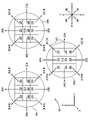
- 複数のマイクロレンズ群を備えた光照射野ディスプレイであって、
各マイクロレンズ群は複数のマイクロレンズを含み、
各マイクロレンズは、その下方に位置づけられた対応するマイクロLEDデバイスアレイを有し、当該マイクロLEDデバイスアレイは複数のマイクロLEDデバイスを備え、
前記マイクロLEDデバイスアレイの各マイクロLEDデバイスは、前記マイクロLEDデバイスのアクティブ層積層体によって発せられる光をコリメートし且つ当該コリメートされた光を、前記マイクロLEDデバイスの上方に位置づけられたマイクロレンズに方向付けるように形成された反射面を備え、
マイクロレンズ群の1つ又は複数のマイクロレンズが、マイクロLEDデバイスのそれぞれからの前記コリメートされた光を、対応する複数の方向に方向付ける凹形状を有し、前記方向のそれぞれは角度視野に対応し、角度視野の数は角度分解能に対応する、
光照射野ディスプレイ。 - マイクロレンズ群の隣接する3つのマイクロレンズが、当該3つのマイクロレンズの中心が正三角形を形成するように配置されている、請求項1に記載の光照射野ディスプレイ。
- 前記マイクロレンズ群が少なくとも3つのマイクロレンズを含み、各マイクロLEDデバイスアレイのマイクロLEDデバイスは互いに同じ色の光を発し、前記マイクロレンズのそれぞれの下方にそれぞれ位置付けられたマイクロLEDデバイスアレイは光を集合的に発し、1つのマイクロレンズの下方のマイクロLEDデバイスアレイの光の色は、他のマイクロレンズの下方のマイクロLEDデバイスアレイの光の色とは異なる、請求項1に記載の光照射野ディスプレイ。
- 前記マイクロLEDデバイスの1つ又は複数は、
アクティブ層積層体と、
前記アクティブ層積層体上に配置された透明導電性酸化物(TCO)層であって、当該透明導電性酸化物(TCO)層と前記アクティブ層積層体の少なくとも一部分は実質的に円形放物形状を成す、透明導電性酸化物(TCO)層と、
前記透明導電性酸化物(TCO)層上に配置された電気絶縁層であって、内部に開口が形成されている電気絶縁層と、
前記電気絶縁層上に配置された反射層であって、前記反射層は前記反射面を備え、前記反射面の対称軸は前記アクティブ層積層体の平行面に直交する、反射層と
を備える、請求項3に記載の光照射野ディスプレイ。 - 少なくとも3つのマイクロレンズのそれぞれの下方にそれぞれ位置付けられた前記マイクロLEDデバイスアレイのそれぞれから集合的に発せられる光の色が、赤、緑、及び青を含む、請求項4に記載の光照射野ディスプレイ。
- 前記マイクロLEDデバイスアレイの前記マイクロLEDデバイスが、六角形パターンに配置される、請求項1に記載の光照射野ディスプレイ。
- 複数のピクセルを備えた光照射野ディスプレイであって、前記ピクセルの数は空間分解能に対応し、各ピクセルは、
複数のマイクロLEDアレイであって、各マイクロLEDアレイは単色の複数のマイクロLEDデバイスを備える、マイクロLEDアレイと、
各マイクロLEDアレイの上方にそれぞれ位置付けられた複数のマイクロレンズと
を備え、マイクロLEDアレイの各マイクロLEDデバイスは、コリメートされた光を対応するマイクロレンズに方向付けるように構成され、前記対応するマイクロレンズは、前記複数のマイクロLEDデバイスからの前記コリメートされた光の方向を、対応する複数の方向へと変更する凹形状を有し、対応する複数の角度視野を提供し、角度視野の数は角度分解能に対応する、
光照射野ディスプレイ。 - ピクセルが複数のマイクロLEDアレイを含み、各マイクロLEDアレイの上には複数のマイクロレンズの対応するマイクロレンズが重なるように位置付けられており、前記マイクロLEDアレイの少なくとも2つによって供給される光の色が互いに異なる、請求項7に記載の光照射野ディスプレイ。
- 各ピクセルが、三角構成に配置された3つの凹レンズを備える、請求項7に記載の光照射野ディスプレイ。
- 各マイクロLEDアレイが、少なくとも3つのマイクロLEDデバイスを備える、請求項7に記載の光照射野ディスプレイ。
- 各マイクロLEDアレイの前記複数のマイクロLEDデバイスが、六角形パターンに配置される、請求項7に記載の光照射野ディスプレイ。
- 複数のピクセルを備えた光照射野ディスプレイであって、ピクセルの数は空間分解能に対応し、各ピクセルは、
基板パネル上に形成された複数の光方向付け特徴と、
前記複数の光方向付け特徴のそれぞれの下方に位置付けられた対応する複数のマイクロLEDデバイスと
を備え、前記対応するマイクロLEDデバイスは、アクティブ層積層体と、当該アクティブ層積層体によって発せられた光をコリメートし且つ当該コリメートされた光を対応する前記光方向付け特徴に方向付けるために使用される反射層とを備え、
前記複数の光方向付け特徴は、マイクロLEDデバイスのそれぞれからの前記コリメートされた光を、対応する複数の方向に方向付け、前記方向のそれぞれは角度視野に対応し、角度視野の数は角度分解能に対応する、
光照射野ディスプレイ。 - 前記基板パネルが前記複数のピクセルに広がる、請求項12に記載の光照射野ディスプレイ。
- 同じ色の光を発するマイクロLEDデバイスが、直線状ストリップ又はクラスタとして配置される、請求項12に記載の光照射野ディスプレイ。
- 前記直線状ストリップ又はクラスタが、アレイ状に位置付けられる、請求項14に記載の光照射野ディスプレイ。
- 前記反射層が、実質的に円形放物面鏡を形成する、請求項12に記載の光照射野ディスプレイ。
- 前記マイクロLEDデバイスの1つ又は複数が、
前記アクティブ層積層体と、
前記アクティブ層積層体上に配置された透明導電性酸化物(TCO)層であって、当該透明導電性酸化物(TCO)層と前記アクティブ層積層体の少なくとも一部分は実質的に円形放物形状を成す、透明導電性酸化物(TCO)層と、
前記透明導電性酸化物(TCO)層上に配置された電気絶縁層であって、内部に開口が形成されている電気絶縁層と、
前記電気絶縁層上に配置された前記反射層であって、前記反射層は反射面を備え、前記反射面の対称軸は前記アクティブ層積層体の平行面に直交する、反射層と
を備える、請求項16に記載の光照射野ディスプレイ。
Applications Claiming Priority (3)
| Application Number | Priority Date | Filing Date | Title |
|---|---|---|---|
| US201662432156P | 2016-12-09 | 2016-12-09 | |
| US62/432,156 | 2016-12-09 | ||
| PCT/US2017/065563 WO2018107150A1 (en) | 2016-12-09 | 2017-12-11 | Collimated led light field display |
Publications (3)
| Publication Number | Publication Date |
|---|---|
| JP2020501192A JP2020501192A (ja) | 2020-01-16 |
| JP2020501192A5 JP2020501192A5 (ja) | 2021-01-28 |
| JP7077320B2 true JP7077320B2 (ja) | 2022-05-30 |
Family
ID=62487885
Family Applications (1)
| Application Number | Title | Priority Date | Filing Date |
|---|---|---|---|
| JP2019530717A Active JP7077320B2 (ja) | 2016-12-09 | 2017-12-11 | コリメートされたledの光照射野ディスプレイ |
Country Status (5)
| Country | Link |
|---|---|
| US (2) | US10256382B2 (ja) |
| JP (1) | JP7077320B2 (ja) |
| KR (1) | KR20190085516A (ja) |
| CN (1) | CN109983392B (ja) |
| WO (1) | WO2018107150A1 (ja) |
Families Citing this family (12)
| Publication number | Priority date | Publication date | Assignee | Title |
|---|---|---|---|---|
| GB201420860D0 (en) * | 2014-11-24 | 2015-01-07 | Infiniled Ltd | Micro-LED device |
| CN113014906B (zh) | 2016-04-12 | 2023-06-30 | 奎蒂安特有限公司 | 3d场景重建方法、系统及计算机程序存储介质 |
| CN109983392B (zh) | 2016-12-09 | 2021-02-23 | 应用材料公司 | 准直led光场显示器 |
| US10490599B2 (en) | 2017-07-13 | 2019-11-26 | Applied Materials, Inc. | Collimated, directional micro-LED light field display |
| EP3524967B1 (en) * | 2018-02-07 | 2024-01-31 | OMRON Corporation | Image inspection device and lighting device |
| US10999573B2 (en) * | 2018-04-25 | 2021-05-04 | Raxium, Inc. | Partial light field display architecture |
| CN112470191A (zh) | 2018-05-02 | 2021-03-09 | 奎蒂安特有限公司 | 用于处理具有几乎无限细节的场景的编解码器 |
| CN109283692A (zh) * | 2018-11-23 | 2019-01-29 | 南方科技大学 | 一种显示装置和显示装置的驱动方法 |
| KR20200104102A (ko) * | 2019-02-26 | 2020-09-03 | 삼성전자주식회사 | 다중핀홀을 이용한 3차원 홀로그래픽 디스플레이 및 그 동작방법 |
| US11700510B2 (en) | 2021-02-12 | 2023-07-11 | Oracle International Corporation | Methods, systems, and computer readable media for short message delivery status report validation |
| US20220302101A1 (en) * | 2021-03-16 | 2022-09-22 | Raxium, Inc. | Method for display manufacturing using groups of micro-leds and micro-led arrays |
| WO2023039615A2 (en) * | 2022-11-02 | 2023-03-16 | Futurewei Technologies, Inc. | Device having optical see-through 3d display |
Citations (7)
| Publication number | Priority date | Publication date | Assignee | Title |
|---|---|---|---|---|
| JP2012231122A (ja) | 2011-04-15 | 2012-11-22 | Mitsubishi Chemicals Corp | 窒化物系発光ダイオード素子とその製造方法 |
| US20130207964A1 (en) | 2012-02-15 | 2013-08-15 | Rod G. Fleck | Imaging structure with embedded light sources |
| WO2014049774A1 (ja) | 2012-09-27 | 2014-04-03 | 富士機械製造株式会社 | 半導体素子の電極構造及びその製造方法 |
| US20140300709A1 (en) | 2011-10-20 | 2014-10-09 | Seereal Technologies S.A. | Display device and method for representing a three-dimensional scene |
| WO2016016460A1 (en) | 2014-07-31 | 2016-02-04 | Infiniled Limited | A colour iled display on silicon |
| JP2016526276A (ja) | 2013-04-22 | 2016-09-01 | オスラム オプト セミコンダクターズ ゲゼルシャフト ミット ベシュレンクテル ハフツングOsram Opto Semiconductors GmbH | 光学系配置構造および表示装置 |
| CN105959672A (zh) | 2016-05-03 | 2016-09-21 | 苏州苏大维格光电科技股份有限公司 | 基于主动发光型显示技术的裸眼三维显示装置 |
Family Cites Families (31)
| Publication number | Priority date | Publication date | Assignee | Title |
|---|---|---|---|---|
| HU0000752D0 (en) | 2000-02-21 | 2000-04-28 | Pixel element for three-dimensional screen | |
| US7800121B2 (en) * | 2002-08-30 | 2010-09-21 | Lumination Llc | Light emitting diode component |
| US7112916B2 (en) | 2002-10-09 | 2006-09-26 | Kee Siang Goh | Light emitting diode based light source emitting collimated light |
| IE20040308A1 (en) | 2003-05-02 | 2004-11-17 | Univ College Cork Nat Univ Ie | Light emitting diodes and the manufacture thereof |
| EP1735844B1 (en) | 2004-03-18 | 2019-06-19 | Phoseon Technology, Inc. | Use of a high-density light emitting diode array comprising micro-reflectors for curing applications |
| US7045375B1 (en) | 2005-01-14 | 2006-05-16 | Au Optronics Corporation | White light emitting device and method of making same |
| US20060238545A1 (en) | 2005-02-17 | 2006-10-26 | Bakin Dmitry V | High-resolution autostereoscopic display and method for displaying three-dimensional images |
| US7771917B2 (en) * | 2005-06-17 | 2010-08-10 | Micron Technology, Inc. | Methods of making templates for use in imprint lithography |
| US8729580B2 (en) * | 2005-12-06 | 2014-05-20 | Toshiba Techno Center, Inc. | Light emitter with metal-oxide coating |
| JP2007173393A (ja) * | 2005-12-20 | 2007-07-05 | Denso Corp | レーザ装置 |
| JP2010181843A (ja) * | 2009-02-09 | 2010-08-19 | Seiko Epson Corp | 印刷版の製造方法および印刷版製造用光硬化性液体 |
| NL2004945A (en) * | 2009-08-14 | 2011-02-15 | Asml Netherlands Bv | Imprint lithography apparatus and method. |
| NL2005865A (en) * | 2010-02-16 | 2011-08-17 | Asml Netherlands Bv | Imprint lithography. |
| WO2012081569A1 (ja) | 2010-12-16 | 2012-06-21 | シャープ株式会社 | 発光素子、調光素子、表示装置および照明装置 |
| GB201202222D0 (en) | 2012-02-09 | 2012-03-28 | Mled Ltd | Enhanced light extraction |
| EP2845047A4 (en) | 2012-04-30 | 2015-04-15 | Hewlett Packard Development Co | SYSTEM AND METHOD FOR PRESENTING 3D IMAGES FOR DISPLAY |
| US20130314780A1 (en) * | 2012-05-25 | 2013-11-28 | 3M Innovative Properties Company | Lens designs for integral imaging 3d displays |
| GB201215632D0 (en) | 2012-09-03 | 2012-10-17 | Infiniled Ltd | Optical device |
| JP2014086863A (ja) * | 2012-10-23 | 2014-05-12 | Sony Corp | 撮像装置、および画像処理方法、並びにプログラム |
| US9888231B2 (en) | 2013-09-11 | 2018-02-06 | Boe Technology Group Co., Ltd. | Three-dimensional display device |
| GB2521176A (en) | 2013-12-11 | 2015-06-17 | Infiniled Ltd | Apparatus and method for profiling a beam of a light emitting semiconductor device |
| CN104914586B (zh) * | 2014-03-11 | 2020-07-24 | 北京三星通信技术研究有限公司 | 集成成像显示设备 |
| GB2526078A (en) | 2014-05-07 | 2015-11-18 | Infiniled Ltd | Methods and apparatus for improving micro-LED devices |
| GB201418810D0 (en) | 2014-10-22 | 2014-12-03 | Infiniled Ltd | Display |
| GB201420860D0 (en) | 2014-11-24 | 2015-01-07 | Infiniled Ltd | Micro-LED device |
| CN104519347B (zh) * | 2014-12-10 | 2017-03-01 | 北京智谷睿拓技术服务有限公司 | 光场显示控制方法和装置、光场显示设备 |
| US9983337B2 (en) * | 2015-08-07 | 2018-05-29 | Samsung Electronics Co., Ltd. | Light emitting diode display apparatus |
| JP2017040818A (ja) * | 2015-08-20 | 2017-02-23 | パナソニックIpマネジメント株式会社 | 発光素子 |
| US10514552B2 (en) | 2015-11-20 | 2019-12-24 | Chen Duan Jun | Auto stereoscopic three-dimensional panel display systems and methods supporting improved fidelity display to multiple simultaneous viewers |
| CN109983392B (zh) | 2016-12-09 | 2021-02-23 | 应用材料公司 | 准直led光场显示器 |
| US10490599B2 (en) * | 2017-07-13 | 2019-11-26 | Applied Materials, Inc. | Collimated, directional micro-LED light field display |
-
2017
- 2017-12-11 CN CN201780068578.2A patent/CN109983392B/zh active Active
- 2017-12-11 US US15/837,654 patent/US10256382B2/en active Active
- 2017-12-11 JP JP2019530717A patent/JP7077320B2/ja active Active
- 2017-12-11 WO PCT/US2017/065563 patent/WO2018107150A1/en active Application Filing
- 2017-12-11 KR KR1020197015185A patent/KR20190085516A/ko not_active Application Discontinuation
-
2019
- 2019-03-29 US US16/369,574 patent/US10559730B2/en active Active
Patent Citations (7)
| Publication number | Priority date | Publication date | Assignee | Title |
|---|---|---|---|---|
| JP2012231122A (ja) | 2011-04-15 | 2012-11-22 | Mitsubishi Chemicals Corp | 窒化物系発光ダイオード素子とその製造方法 |
| US20140300709A1 (en) | 2011-10-20 | 2014-10-09 | Seereal Technologies S.A. | Display device and method for representing a three-dimensional scene |
| US20130207964A1 (en) | 2012-02-15 | 2013-08-15 | Rod G. Fleck | Imaging structure with embedded light sources |
| WO2014049774A1 (ja) | 2012-09-27 | 2014-04-03 | 富士機械製造株式会社 | 半導体素子の電極構造及びその製造方法 |
| JP2016526276A (ja) | 2013-04-22 | 2016-09-01 | オスラム オプト セミコンダクターズ ゲゼルシャフト ミット ベシュレンクテル ハフツングOsram Opto Semiconductors GmbH | 光学系配置構造および表示装置 |
| WO2016016460A1 (en) | 2014-07-31 | 2016-02-04 | Infiniled Limited | A colour iled display on silicon |
| CN105959672A (zh) | 2016-05-03 | 2016-09-21 | 苏州苏大维格光电科技股份有限公司 | 基于主动发光型显示技术的裸眼三维显示装置 |
Also Published As
| Publication number | Publication date |
|---|---|
| KR20190085516A (ko) | 2019-07-18 |
| US10559730B2 (en) | 2020-02-11 |
| US20190229246A1 (en) | 2019-07-25 |
| JP2020501192A (ja) | 2020-01-16 |
| CN109983392B (zh) | 2021-02-23 |
| CN109983392A (zh) | 2019-07-05 |
| US10256382B2 (en) | 2019-04-09 |
| US20180166616A1 (en) | 2018-06-14 |
| WO2018107150A1 (en) | 2018-06-14 |
Similar Documents
| Publication | Publication Date | Title |
|---|---|---|
| JP7077320B2 (ja) | コリメートされたledの光照射野ディスプレイ | |
| TWI797132B (zh) | 準直、定向的微型發光二極體光場顯示器及其形成方法 | |
| US20230101837A1 (en) | Display device having light emitting stacked structure | |
| CN109643724B (zh) | 高密度像素化的led和器件及其方法 | |
| US10100997B2 (en) | Semiconductor light source and driving aid system for a motor vehicle comprising such a source | |
| KR20160003746A (ko) | 광학 어레이 및 표시 장치 | |
| KR20130029798A (ko) | 다차원 led 어레이 시스템 및 관련 방법 및 구조 | |
| US20240120446A1 (en) | Light-emitting diodes with integrated optical elements | |
| US11482566B2 (en) | Light emitting device for display and display apparatus having the same | |
| KR20070102089A (ko) | 발광 소자 모듈 및 그 제조 방법 | |
| US11169393B2 (en) | 3D display element | |
| KR101460380B1 (ko) | 혼합광 생성 장치 및 그러한 장치에 대한 제조 방법 | |
| WO2018114527A1 (en) | Led array module | |
| JP4771040B2 (ja) | El照明装置 | |
| KR20210005175A (ko) | 자외선 레이저를 사용한 led 표면 개질 | |
| US11973069B2 (en) | Fabrication of LED arrays and LED array light engines | |
| US11869923B2 (en) | Light-emitting array with dielectric light collection structures | |
| US20120299034A1 (en) | Collimating light emitting device and manufacturing method thereof | |
| KR20230159593A (ko) | Led 어레이들 및 디스플레이들을 위한 패터닝된 반사성 그리드들 | |
| CN117995865A (zh) | 微型led芯片、显示模组及电子设备 | |
| JP2015072970A (ja) | 発光素子 |
Legal Events
| Date | Code | Title | Description |
|---|---|---|---|
| A521 | Request for written amendment filed |
Free format text: JAPANESE INTERMEDIATE CODE: A523 Effective date: 20201211 |
|
| A621 | Written request for application examination |
Free format text: JAPANESE INTERMEDIATE CODE: A621 Effective date: 20201211 |
|
| A977 | Report on retrieval |
Free format text: JAPANESE INTERMEDIATE CODE: A971007 Effective date: 20210922 |
|
| A131 | Notification of reasons for refusal |
Free format text: JAPANESE INTERMEDIATE CODE: A131 Effective date: 20211005 |
|
| A601 | Written request for extension of time |
Free format text: JAPANESE INTERMEDIATE CODE: A601 Effective date: 20220104 |
|
| A521 | Request for written amendment filed |
Free format text: JAPANESE INTERMEDIATE CODE: A523 Effective date: 20220304 |
|
| TRDD | Decision of grant or rejection written | ||
| A01 | Written decision to grant a patent or to grant a registration (utility model) |
Free format text: JAPANESE INTERMEDIATE CODE: A01 Effective date: 20220426 |
|
| A61 | First payment of annual fees (during grant procedure) |
Free format text: JAPANESE INTERMEDIATE CODE: A61 Effective date: 20220518 |
|
| R150 | Certificate of patent or registration of utility model |
Ref document number: 7077320 Country of ref document: JP Free format text: JAPANESE INTERMEDIATE CODE: R150 |