JP7033863B2 - Pachinko machine - Google Patents
Pachinko machine Download PDFInfo
- Publication number
- JP7033863B2 JP7033863B2 JP2017143723A JP2017143723A JP7033863B2 JP 7033863 B2 JP7033863 B2 JP 7033863B2 JP 2017143723 A JP2017143723 A JP 2017143723A JP 2017143723 A JP2017143723 A JP 2017143723A JP 7033863 B2 JP7033863 B2 JP 7033863B2
- Authority
- JP
- Japan
- Prior art keywords
- board
- frame
- unit
- design
- effect
- Prior art date
- Legal status (The legal status is an assumption and is not a legal conclusion. Google has not performed a legal analysis and makes no representation as to the accuracy of the status listed.)
- Active
Links
Images


Description
本発明は、遊技動作に起因する抽選処理によって大当り状態を発生させる遊技機に関し、特に、個性的な遊技枠を備えた遊技機に関する。 The present invention relates to a gaming machine that generates a big hit state by a lottery process caused by a gaming operation, and more particularly to a gaming machine provided with a unique gaming frame.
パチンコ機などの弾球遊技機は、遊技盤に設けた図柄始動口と、複数の表示図柄による一連の図柄変動態様を表示する図柄表示部と、開閉板が開閉される大入賞口などを備えて構成されている。そして、図柄始動口に設けられた検出スイッチが遊技球の通過を検出すると入賞状態となり、遊技球が賞球として払出された後、図柄表示部では表示図柄が所定時間変動される。その後、7・7・7などの所定の態様で図柄が停止すると大当り状態となり、大入賞口が繰返し開放されて、遊技者に有利な遊技状態を発生させている。 A ball game machine such as a pachinko machine is equipped with a symbol start opening provided on the game board, a symbol display unit that displays a series of symbol variation modes by a plurality of display symbols, and a large winning opening for opening and closing the opening / closing plate. It is composed of. Then, when the detection switch provided at the symbol start port detects the passage of the game ball, the winning state is set, and after the game ball is paid out as the prize ball, the displayed symbol is changed for a predetermined time on the symbol display unit. After that, when the symbol is stopped in a predetermined mode such as 7, 7, 7, a big hit state is reached, and the big winning opening is repeatedly opened to generate a game state advantageous to the player.
このような遊技状態を発生させるか否かは、図柄始動口に遊技球が入賞したことを条件に実行される大当り抽選で決定されており、上記の図柄変動動作は、この抽選結果を踏まえたものとなっている。例えば、抽選結果が当選状態である場合には、リーチアクションなどと称される演出動作を20秒前後実行し、その後、特別図柄を整列させている。一方、ハズレ状態の場合にも、同様のリーチアクションが実行されることがあり、この場合には、遊技者は、大当り状態になることを強く念じつつ演出動作の推移を注視することになる。そして、図柄変動動作の終了時に、停止ラインに所定図柄が揃えば、大当り状態であることが遊技者に保証されたことになる。 Whether or not to generate such a game state is determined by a big hit lottery executed on the condition that the game ball wins at the symbol start opening, and the above symbol variation operation is based on this lottery result. It has become a thing. For example, when the lottery result is in the winning state, an effect operation called a reach action or the like is executed for about 20 seconds, and then special symbols are arranged. On the other hand, the same reach action may be executed even in the case of a lost state, and in this case, the player pays close attention to the transition of the production operation while strongly paying attention to the big hit state. Then, if the predetermined symbols are aligned on the stop line at the end of the symbol variation operation, the player is guaranteed to be in the big hit state.
この種の遊技機は、一般に、長期間使用される枠側部材と、機種毎に変更される盤側部材とに区分され、遊技ホールに設置された枠側部材に盤側部材を取り付けることで完成状態となる。そして、機種変更時には、古い盤側部材を枠側部材から取り外した上で、新規の盤側部材を取り付けるものの、それまでの枠側部材は、そのまま使用されることになる(特許文献1~特許文献5)。
This type of gaming machine is generally divided into a frame-side member that is used for a long period of time and a board-side member that is changed for each model, and by attaching the board-side member to the frame-side member installed in the game hall. It will be in a completed state. When changing the model, the old board-side member is removed from the frame-side member and a new board-side member is attached, but the frame-side member up to that point is used as it is (
そのため、枠側部材のデザインを個性化することができないという問題がある。すなわち、枠側部材を個性的なデザインにすると、特定の機種に対しては、その機種が実現しようとする演出コンセプトとぴったりマッチするが、別の機種では、不自然さが否めないという問題がある。 Therefore, there is a problem that the design of the frame side member cannot be individualized. In other words, if the frame side member has a unique design, it matches exactly with the production concept that the model is trying to realize for a specific model, but there is a problem that unnaturalness cannot be denied for another model. be.
本発明は、上記の問題点に鑑みてなされたものであって、機種毎の演出コンセプトに対応して、枠側部材のデザインを変更しても適切に動作する遊技機を提供することを目的とする。 The present invention has been made in view of the above problems, and an object of the present invention is to provide a gaming machine that operates appropriately even if the design of the frame side member is changed in accordance with the production concept for each model. And.
上記の目的を達成するため、本発明は、所定の抽選処理の抽選結果に対応して、画像演出、ランプ演出、又は、音声演出の全部又は一部を実行する遊技機であって、前記遊技機は、演出動作を制御するコンピュータ回路を保持する遊技盤と、複数の部材を備えた枠側部材と、を有して構成され、前記枠側部材は、外枠を構成する第1部材と、前記第1部材に装着される第2部材と、前記第2部材に装着される第3部材と、前記第3部材に変更可能に装着される変更部材と、を有して構成され、前記変更部材に対応する前記遊技盤が、前記第2部材に取り外し可能に装着され、前記変更部材は、前記遊技盤に対応する判別コードを保有すると共に、演出動作に寄与する駆動装置を保有して構成され、前記コンピュータ回路には、クロック信号を出力すると共に、出力するクロック信号に同期して、前記判別コードのシリアル信号を受信する第1シリアルポートと、クロック信号に同期して、前記駆動装置を駆動する駆動データを出力する第2シリアルポートが設けられ、前記コンピュータ回路は、電源投入時、前記変更部材から、第1シリアルポートを経由して前記判別コードを取得して、前記変更部材が、前記遊技盤に対応する部材か否かの整合判定を行い、整合しない場合には異常報知を実行するよう構成されている。 In order to achieve the above object, the present invention is a gaming machine that executes all or part of an image effect, a lamp effect, or a sound effect in response to a lottery result of a predetermined lottery process. The machine is configured to include a game board that holds a computer circuit that controls an effect operation, and a frame-side member having a plurality of members, and the frame-side member is a first member that constitutes an outer frame. A second member mounted on the first member, a third member mounted on the second member, and a changeable member mutatably mounted on the third member. The game board corresponding to the change member is detachably attached to the second member, and the change member has a determination code corresponding to the game board and a drive device that contributes to the effect operation. The computer circuit is configured to have a first serial port that outputs a clock signal and receives the serial signal of the discrimination code in synchronization with the output clock signal, and the drive device in synchronization with the clock signal. A second serial port for outputting drive data is provided, and when the power is turned on, the computer circuit acquires the discrimination code from the change member via the first serial port, and the change member obtains the determination code. , It is configured to perform a matching determination as to whether or not the member corresponds to the game board, and to execute an abnormality notification if the members do not match.
本発明では、前記コンピュータ回路は、電源投入時、前記変更部材から前記判別コードを取得して、遊技盤と変更部材の整合性判定を行い、整合しない場合には異常報知を実行するので、不適切な動作が未然回避される。 In the present invention, when the power is turned on, the computer circuit acquires the discrimination code from the change member, determines the consistency between the game board and the change member, and if they do not match, the abnormality notification is executed. Appropriate operation is avoided .
判別コードによる整合性判定は、電源投入時に限るのが好適であり、整合性判定に合格した後は、定時的に、意匠コードを取得して、演出動作に反映されるのが好ましい。It is preferable that the consistency determination by the determination code is limited to the time when the power is turned on, and after passing the consistency determination, it is preferable to acquire the design code on a regular basis and reflect it in the effect operation.
本発明によれば、機種毎の演出コンセプトに対応して、枠側部材のデザインを変更しても適切に動作する遊技機を実現することができる。 According to the present invention, it is possible to realize a gaming machine that operates appropriately even if the design of the frame side member is changed according to the production concept for each model.
以下、実施例に基づいて本発明を詳細に説明する。図1に示す通り、実施例の遊技機GMは、長期間変更なく遊技ホールで使用される汎用部GERと、機種変更毎に変更可能な変更部CHGと、に大別される。 Hereinafter, the present invention will be described in detail based on examples. As shown in FIG. 1, the gaming machine GM of the embodiment is roughly classified into a general-purpose section GER used in a gaming hall without change for a long period of time and a changing section CHG that can be changed for each model change.
図示の実施例の場合、汎用部GERは、遊技ホールの島構造体に着脱可能に装着される矩形枠状の木製外枠1と、木製外枠1に対して開閉可能に枢着される内枠2と、内枠2に対して開閉可能に枢着される前枠本体3と、で構成されている。
In the case of the illustrated embodiment, the general-purpose unit GER has a rectangular frame-shaped wooden
一方、変更部CHGは、内枠2の表側から着脱自在に装着される遊技盤4(図2(b)参照)と、前枠本体3に着脱自在に装着される枠ユニット5と、枠ユニット5に着脱自在に装着される意匠ユニット6とで構成されている。
On the other hand, the changing portion CHG includes a game board 4 (see FIG. 2B) that is detachably mounted from the front side of the
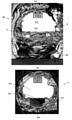
そして、完成状態では、図2(a)に示す正面図の状態となる。なお、この遊技機GMを、図9に示す回路構成図で説明する場合には、枠側部材GM1が、汎用部GERと、枠ユニット5と、意匠ユニット6とで構成され、盤側部材GM2が、遊技盤4(図2(b))で構成されることになる。
Then, in the completed state, it is in the state of the front view shown in FIG. 2 (a). When this gaming machine GM is described with reference to the circuit configuration diagram shown in FIG. 9, the frame-side member GM1 is composed of a general-purpose unit GER, a
本実施例に特徴的な変更部CHGについて説明する前に、先ず、図2に基づいて、遊技機GMの全体構成を概略的に説明する。実施例の遊技機GMは、前枠本体3の左側と、意匠ユニット6には、LEDランプなどによる電飾ランプが配置されている。また、図1に示す通り、前枠本体3の上部の左右位置と、内枠2の下部右側には、合計3個のスピーカSPが配置されている。
Before explaining the modified CHG characteristic of the present embodiment, first, the overall configuration of the gaming machine GM will be schematically described with reference to FIG. 2. In the gaming machine GM of the embodiment, an illuminated lamp such as an LED lamp is arranged on the left side of the front frame
図2(a)に示す通り、前枠本体3の最下部の右側には、遊技球を発射するための発射ハンドルHDが設けられている。その他、前枠本体3には、遊技球を貯留する貯留皿や、カード式球貸し機に対する球貸し操作用の操作パネルが設けられ、適宜な球貸動作や貯留動作が可能となっている。
As shown in FIG. 2A, a firing handle HD for launching a game ball is provided on the lower right side of the lowermost portion of the front frame
図2(b)に示すように、遊技盤4の略中央には、大型の液晶カラーディスプレイで構成されたメイン表示装置DS1が配置され、その下方には、小型の液晶カラーディスプレイで構成されたサブ表示装置DS2が配置されている。
As shown in FIG. 2B, a main display device DS1 composed of a large liquid crystal color display is arranged substantially in the center of the
サブ表示装置DS2は、4個の可動役物(図示では隠蔽状態)に保持されており、メイン表示装置DS1の前面を、昇降可能に構成されている。また、サブ表示装置DS2は、その上昇位置において、可動役物に保持された状態で回転可能に構成されている。なお、何れの動作状態でも、サブ表示装置DS2では、適宜な画像演出が実行されている。 The sub-display device DS2 is held by four movable objects (concealed state in the figure), and is configured to be able to move up and down the front surface of the main display device DS1. Further, the sub-display device DS2 is configured to be rotatable in a raised position while being held by a movable accessory. In any operating state, the sub-display device DS2 is performing an appropriate image effect.
メイン表示装置DS1は、大当り状態に係わる特定図柄を変動表示すると共に背景画像や各種のキャラクタなどをアニメーション的に表示する装置である。そして、メイン表示装置DS1では、特定図柄の変動表示動作と共に、大当り状態の招来を期待させるリーチ演出や、予告演出などが実行されることがある。なお、予告演出としては、サブ表示装置DS2を保持する可動役物の出現や、サブ表示装置DS2の回転動作などが含まれる。 The main display device DS1 is a device that displays a specific symbol related to a jackpot state in a variable manner and displays a background image, various characters, and the like in an animation manner. Then, in the main display device DS1, along with the variable display operation of the specific symbol, a reach effect that expects a big hit state to be invited, a notice effect, and the like may be executed. The notice effect includes the appearance of a movable accessory holding the sub-display device DS2, the rotation operation of the sub-display device DS2, and the like.
本実施例では、メイン表示装置DS1の左側と右側には遊技球が落下移動する円弧通路が形成され、左側通路の底部には図柄始動口STRが配設され、右側通路の底部には、大入賞口ATCが配設されている。 In this embodiment, an arc passage through which the game ball falls and moves is formed on the left side and the right side of the main display device DS1, a symbol start port STR is arranged at the bottom of the left side passage, and a large size is provided at the bottom of the right side passage. A winning opening ATC is arranged.
各入賞口の内部には、検出スイッチが配置されており、検出スイッチが遊技球の通過を検出すると、所定個数の賞球が払出されるようになっている。但し、通常のゲーム状態では、大入賞口ATCの入口が閉鎖されており、メイン表示装置DS1の右側の円弧通路に遊技球を落下させても賞球は得られない。 A detection switch is arranged inside each winning opening, and when the detection switch detects the passage of a game ball, a predetermined number of prize balls are paid out. However, in the normal game state, the entrance of the large winning opening ATC is closed, and even if the game ball is dropped into the arc passage on the right side of the main display device DS1, the prize ball cannot be obtained.
そこで、遊技者は、通常のゲーム状態では、メイン表示装置DS1の左側の円弧通路に遊技球が落下するよう、遊技球を発射することになる(左打ち)。そして、落下した遊技球が図柄始動口STRを通過すると(入賞状態)、保留上限値を超えない限り、大当り抽選処理が実行され、遊技者に有利な遊技状態に移行するか否かが抽選決定される。 Therefore, in the normal game state, the player fires the game ball so that the game ball falls into the arc passage on the left side of the main display device DS1 (left-handed). Then, when the dropped game ball passes through the symbol start opening STR (winning state), the big hit lottery process is executed as long as the hold upper limit value is not exceeded, and it is decided by lottery whether or not to shift to the game state advantageous to the player. Will be done.
但し、この大当り抽選の当否結果に拘らず、メイン表示装置DS1では、遊技球の入賞を契機として、特別図柄の変動動作を伴う一連の画像演出が開始される。また、この画像演出に対応して、背景音楽や演出音を伴う音声演出や、ランプが点滅するランプ演出が実行される。 However, regardless of the result of the big hit lottery, the main display device DS1 starts a series of image effects accompanied by the fluctuation operation of the special symbol, triggered by the winning of the game ball. Further, in response to this image effect, a sound effect accompanied by background music and a production sound, and a lamp effect in which the lamp blinks are executed.
なお、この一連の演出動作に並行して、メイン表示装置DS1やサブ表示装置DS2では、リーチ演出や予告演出が実行されることがある。その後、特別図柄の変動動作が終了ことで、大当り抽選処理の当否結果が遊技者に報知されるようになっている。 In parallel with this series of effect operations, the main display device DS1 and the sub display device DS2 may execute the reach effect and the advance notice effect. After that, when the variable operation of the special symbol is completed, the result of the big hit lottery process is notified to the player.
そして、ゲーム状態が大当り状態に移行すれば、大入賞口ATCの入口が開放されるので、遊技者は、メイン表示装置DS1の右側の円弧通路に遊技球が落下するよう、遊技球を発射することになる(右打ち)。 Then, when the game state shifts to the big hit state, the entrance of the big winning opening ATC is opened, so that the player fires the game ball so that the game ball falls into the arc passage on the right side of the main display device DS1. It will be (right-handed).
大入賞口ATCの動作は、特に限定されないが、典型的な大当り状態では、所定時間が経過し、又は所定数(例えば10個)の遊技球が入賞すると入口が閉じるよう制御される。このような動作は、最大で例えば15回まで継続され、遊技者に有利な状態に制御される。なお、特別図柄の変動後の停止図柄が特別図柄のうちの特定図柄であった場合には、特別遊技の終了後のゲームが高確率状態(確変状態)となるという特典が付与される。 The operation of the big winning opening ATC is not particularly limited, but in a typical big hit state, the entrance is controlled to close when a predetermined time elapses or a predetermined number (for example, 10) of game balls win a prize. Such an operation is continued up to, for example, 15 times, and is controlled in a state advantageous to the player. If the stop symbol after the change of the special symbol is a specific symbol among the special symbols, the privilege that the game after the end of the special game is in a high probability state (probability change state) is given.
以上、遊技機GMの概略動作を説明したので、図1に戻って、変更部CHGについて説明する。図1に示す通り、実施例の枠ユニット5は、水平片50と垂直片51とで、反転L字状に構成されて、前枠本体3の上辺と右辺に沿って着脱可能に固定されている。また、実施例の意匠ユニット6は、縦長に構成されて、枠ユニット5の垂直片51に沿って着脱可能に固定されている。
Since the schematic operation of the gaming machine GM has been described above, the modified portion CHG will be described by returning to FIG. As shown in FIG. 1, the
ここで、枠ユニット5は、一般的な汎用デザインの汎用ユニット5Gと、個性的なデザインの多種類の個性ユニット5Uとに大別され、個性ユニット5Uとして、例えば、ボクシング映画をモチーフにした一連の遊技機で使用されるゴング枠5U1や、アニメ主人公(眼鏡少女)をモチーフした一連の遊技機で使用される眼鏡少女枠5U2や、・・・、○○枠5Uiや、××枠5Ujなどが用意されている。
Here, the
また、意匠ユニット6は、枠ユニット5の種類ごとに、複数個が用意されており、例えば、眼鏡少女枠5U2に対応する意匠ユニット6(図2(a)参照)としては、主人公の衣服の色やデザインが相違する複数種類が用意されている。
Further, a plurality of
このように本実施例では、前枠本体3に装着する枠ユニット5が複数個用意されている上に、枠ユニット5毎に、複数の意匠ユニット6が用意されているので、遊技盤4が意図するゲーム性に合わせて、遊技盤4の周囲を最適に装飾することができる。
As described above, in this embodiment, a plurality of
図3は、枠ユニット5と意匠ユニット6の結合状態(図3(a))と、単体の枠ユニット5(図3(b))と、単体の意匠ユニット6(図3(c))について、各々の正面図を図示したものである。なお、枠ユニット5と意匠ユニット6の結合状態については、図4に、その六面図を図示している。
FIG. 3 shows the combined state of the
また、図5は、枠ユニット5についての六面図であり、図6は、意匠ユニット6についての六面図である。図4の六面図と、図5及び図6の六面図と、を対比することで、枠ユニット5と意匠ユニット6の形状が明らかとなる。
Further, FIG. 5 is a six-view view of the
特に限定されないが、図示の枠ユニット5は、眼鏡少女枠5U2であり、意匠ユニット6には、眼鏡少女枠5U2に対応して、藁人形9が形成されている。なお、実際の意匠ユニット6には、図2に示す通り、遊技盤4の遊技性に合わせた、眼鏡少女の画像が描かれているが、図3~図6では、便宜上、これらの画像表示を省略している。
Although not particularly limited, the illustrated
何れにしても、枠ユニット5には、藁人形9を貫通して、遊技バー10が操作可能に取り付けられている(図3(b)参照)。そして、抽選処理結果が大当り状態であることを示唆する予告演出において、その予告演出の信頼度が高い場合には、遊技バー10の押圧操作が許可されるようになっている。なお、信頼度とは、抽選処理結果が、大当り状態である可能性を意味する。
In any case, the
また、枠ユニット5には、意匠ユニット6から突出する係止片15(図6)を受け入れる開口穴11が設けられている(図3(b)参照)。そして、この開口穴11には、図3や図5の下方に向けて揺動可能な揺動部材12が配置されている。
Further, the
図6に示す通り、係止片15は、断面L字状の板材である。そして、意匠ユニット6を枠ユニット5に組み付ける時には、意匠ユニット6の上部適所を、枠ユニット5に係合させた状態で、枠ユニット5に意匠ユニット6を重合させるべく操作する。すると、係止片15の先端が、開口穴11に突入し、揺動部材12に当接する状態となる。
As shown in FIG. 6, the locking
先に説明した通り、揺動部材12は、鉛直下方に揺動可能に構成されているので、係止片15の先端が更に進入すると、揺動部材12が下方に揺動して、開口穴11に係止片15が没入される。次に、係止片15の没入状態において、適宜なロック部材(不図示)を用いるか、或いは、揺動部材12に弾発力を作用させることによって、揺動部材12を上方に揺動させると、係止片15のフック先端が揺動部材12に係止することになる。
As described above, since the
この時、同様のフック状態が、他の箇所でも実現されるので、意匠ユニット6が、枠ユニット5に対して、正確に位置決めされることになる。そして、この重合状態において、適所をビス止めすることで、意匠ユニット6と枠ユニット5とが、完全な固定状態となる。
At this time, since the same hook state is realized at other places, the
図3に戻って、枠ユニット5の構成の説明を続けると、枠ユニット5の水平片50には、その内部に機種判別基板BD0が配置されている。機種判別基板BD0には、8ビット長の判別コードが固定的に記憶されており、この枠ユニット5が、汎用ユニット5Gであるか、或いは、何れの個性枠5U(5U1,5U2,・・・5Uj)であるかが一意に特定されるようになっている(図3(d)参照)。
Returning to FIG. 3, and continuing the description of the configuration of the
先に説明した通り、枠ユニット5は、遊技盤4に対応しており、電源投入時に判別コードが判定されることで、枠ユニット5と遊技盤4の整合関係が確認可能となっている。そして、万一、枠ユニット5が遊技盤4と整合しない場合には、異常報知動作が実行される。
As described above, the
また、図3(b)に示す通り、枠ユニット5の垂直片51には、意匠ユニット6から突出する遮光板MKを受け入れるフォトインタラプタPI0~PI2(=PIi)が配置され、これに近接して、意匠判別基板BD1が配置されている。そして、遮光板MKとフォトインタラプタPIiとで、意匠判定部13を構成している。
Further, as shown in FIG. 3 (b), photo interrupters PI0 to PI2 (= PIi) for receiving the light-shielding plate MK protruding from the
図7(c)は、意匠判別基板BD1の回路構成を図示したものであり、図7(a)は、遮光板MKとフォトインタラプタPIiとで構成された意匠判定部13を図示したものである。
FIG. 7C illustrates the circuit configuration of the design discrimination substrate BD1, and FIG. 7A illustrates the
この実施例では、意匠判定部13は、3個のフォトインタラプタPI0~PI2を有して構成されている。図示の通り、各フォトインタラプタPIiは、検査光を発光するフォトダイオードDと、検査光を受けるフォトトランジスタTRとを、適宜な隙間GPを介在させて対面させて構成されている。
In this embodiment, the
遮光板MKは、意匠ユニット6に固定された基部MK1と、組付け時にフォトダイオードDとフォトトランジスタTRの隙間GPに突入する突出部MK2とで、断面視が略T字状に形成された透明プラスチック材である。そして、透明な突出部MK2に、マスクシートSHを貼着させることで遮光性能を実現している。
The light-shielding plate MK is a transparent portion formed in a substantially T-shape in cross-sectional view by a base MK1 fixed to the
図示の通り、突出部MK2は、フォトインタラプタPI0~PI2に対応して三分されており、その適所が、マスクシートSHによって遮光部となっている。そのため、各フォトインタラプタPIiの出力Diは、検査光の遮光状態では、0(=L)となり、透光状態では1(=H)となる。 As shown in the figure, the protruding portion MK2 is divided into three parts corresponding to the photo interrupters PI0 to PI2, and the appropriate place thereof is a light-shielding portion by the mask sheet SH. Therefore, the output Di of each photo interrupter PIi is 0 (= L) in the light-shielded state of the inspection light and 1 (= H) in the light-transmitting state.
特に限定されないが、本実施例では、三分された突出部MK2の3箇所のうち、1又は2箇所が遮光部となっており、フォトインタラプタPI2~PI0の出力D2~D0は、図7(b)の通りであり、最高5種類の意匠ユニット6(意匠A~意匠F)を特定できるようになっている。 Although not particularly limited, in this embodiment, one or two of the three portions of the three-divided protruding portions MK2 are light-shielding portions, and the outputs D2 to D0 of the photo interrupters PI2 to PI0 are shown in FIG. 7 ( As shown in b), up to five types of design units 6 (designs A to F) can be specified.
なお、図7(a)の構成では、フォトインタラプタPI2だけが遮光状態となるので、出力D2だけが0となり、意匠ユニット6には、意匠Cの画像が描かれていることになる。
In the configuration of FIG. 7A, since only the photo interrupter PI2 is in a light-shielding state, only the output D2 becomes 0, and the
次に、図5(c)に示す通り、枠ユニット5には、外気導入口H0と、噴出口H1とが形成され、その下方位置には、噴出口H1に連通する噴出機構16(図8参照)が傾斜姿勢で配置されている。なお、噴出機構16は、枠ユニット5の内部に配置されており、図6(c)には、噴出機構16に関して、噴出口H1と連絡穴INだけが現れている。
Next, as shown in FIG. 5 (c), the outside air introduction port H0 and the ejection port H1 are formed in the
この噴出機構16に対応して、意匠ユニット6には、匂い袋17が配置されている(図6(c)参照)。匂い袋17には、遊技機の遊技コンセププトに対応して、適宜な香料が内包されており、所定の予告演出時に限り、匂い袋17の香りが、噴出機構16の噴出口H1から、遊技者に向けて放出されるようになっている。
A
本実施例では、噴出機構16が枠ユニット5に配置される一方、意匠ユニット6には、匂い袋17が配置されている。そのため、意匠ユニット6毎に、主人公の衣服の色やデザインに対応して、匂い袋17の香料を変えることもでき、益々、遊技機毎の個性を発揮させることが可能となる。
In this embodiment, the
図8(a)は、噴出機構16の構成を示す分解斜視図である。図示の通り、噴出機構16は、外気導入口H0から導入された外気を連絡穴INに受ける基礎部材BS0と、基礎部材BS0に連設される第1部材BS1に内蔵されるソレノイド部材SLと、第1部材に連設される第2部材BS2に内蔵される送風部材BLWと、を有して構成されている。先に説明した通り、基礎部材BS0の連絡穴INに近接して、意匠ユニット6には匂い袋17が配置されている。
FIG. 8A is an exploded perspective view showing the configuration of the
図8(b)は、噴出機構16の動作原理を説明する原理図である。なお、実際には、噴出機構16が図8(c)に示す傾斜状態で取り付けられる。矢印(→)に示す通り、香り袋17を経由して連絡穴INに導入された外気は、屈曲する外気通路を経由して、ソレノイド部材SLを内蔵する第1部材BS1に導入される。なお、外気は、連絡穴INに対して、図8(b)の紙面の奥向きに導入される。
FIG. 8B is a principle diagram illustrating the operating principle of the
図8(a)に示す通り、ソレノイド部材SLは、電磁ソレノイドSL1と、阻止部SL2と、阻止部SL2を進退させるプランジャSL3とで構成され、プランジャSL3にはスプリングSPが外装されている。 As shown in FIG. 8A, the solenoid member SL is composed of an electromagnetic solenoid SL1, a blocking portion SL2, and a plunger SL3 for advancing and retreating the blocking portion SL2, and the plunger SL3 is provided with a spring SP.
そのため、電磁ソレノイドSL1が非通電状態であれば、スプリングSPの弾性力によって、プランジャSL3と阻止部SL2が図示左方向に突出して外気通路を遮断する。一方、電磁ソレノイドSL1が通電すると、プランジャSL3が図示右方向に引き込まれることで、外気通路が開放される。 Therefore, when the electromagnetic solenoid SL1 is in a non-energized state, the plunger SL3 and the blocking portion SL2 project to the left in the drawing due to the elastic force of the spring SP to block the outside air passage. On the other hand, when the electromagnetic solenoid SL1 is energized, the plunger SL3 is pulled in to the right in the drawing, so that the outside air passage is opened.
特に限定されないが、本実施例では、信頼度の高い予告演出時に、電磁ソレノイドSL1が通電するよう構成されており、この導通動作に対応して、送風部材BLWが動作するようになっている。 Although not particularly limited, in the present embodiment, the electromagnetic solenoid SL1 is configured to be energized at the time of a highly reliable advance notice effect, and the blower member BLW is operated in response to this conduction operation.
図8(b)や図8(c)は、電磁ソレノイドSL1の導通状態を示しており、第1部材BS1に導入された外気が、第2部材BS2に導入される状態を示している。なお、この外気は、匂い袋17を経由することで、適宜な香りを含んでいる。
8 (b) and 8 (c) show the conduction state of the electromagnetic solenoid SL1, and show the state in which the outside air introduced into the first member BS1 is introduced into the second member BS2. The outside air contains an appropriate scent by passing through the
第2部材BS2には、送風部材BLWが内蔵されており、電磁ソレノイドSL1の通電動作に対応して、送風モータ(ブロワ―)が回転を開始する。そのため、第2部材BS2に導入された香りを含んだ外気が、噴出口H1から噴出されることになる。なお、外気は、噴出口H1に対して、図8(b)の紙面の手前向きに、長い溜め息のように噴出される。なお、噴出回数は、予告演出の信頼度に応じて、一回だけで終わるか、或いは、複数回繰り返される。 The second member BS2 has a built-in blower member BLW, and the blower motor (blower) starts to rotate in response to the energization operation of the electromagnetic solenoid SL1. Therefore, the outside air containing the scent introduced into the second member BS2 is ejected from the ejection port H1. The outside air is blown out toward the ejection port H1 toward the front of the paper surface of FIG. 8B like a long sigh. It should be noted that the number of times of ejection may be completed only once or repeated a plurality of times depending on the reliability of the advance notice effect.
図5(c)に示す通り、この噴出口H1は、遊技者に向けて開放されており、所定の予告演出時に、遊技者が送風や香りを感じることで、大当り状態の招来を所定の高い信頼度で期待することになる。 As shown in FIG. 5 (c), this spout H1 is open to the player, and the player feels a blast or a scent at the time of a predetermined advance notice effect, so that a big hit state is invited at a predetermined high level. You will expect it with reliability.
このように、本実施例では、映像、音声、ランプ、役物による予告演出に加えて、送風や香りによる演出動作が可能となっており、極めて斬新な予告演出が実現される。しかも、遊技性に合わせた、異なる個性的な香りを放出することができる。なお、通常は、送風部材BLWが動作を停止しており、また、電磁ソレノイドSL1が非通電状態であるので、遊技者が、送風や香りを感じることはない。 As described above, in this embodiment, in addition to the advance notice effect by the video, the sound, the lamp, and the accessory, the effect operation by the blast and the scent is possible, and the extremely novel advance notice effect is realized. Moreover, it is possible to emit different unique scents according to the playability. Normally, since the blower member BLW is stopped and the electromagnetic solenoid SL1 is in a non-energized state, the player does not feel the blower or the scent.
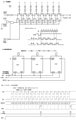
以上、遊技機の機器構成について説明したので、次に、回路構成について説明する。図9は、上記した各動作を実現するパチンコ機GMの全体回路構成を示すブロック図である。また、図10は、図9の一部を詳細に図示したものであり、演出制御基板22と、モータ駆動基板37などとの接続状態を図示したものである。 Now that the equipment configuration of the gaming machine has been described, the circuit configuration will be described next. FIG. 9 is a block diagram showing an overall circuit configuration of the pachinko machine GM that realizes each of the above operations. Further, FIG. 10 shows a part of FIG. 9 in detail, and shows the connection state between the effect control board 22 and the motor drive board 37 and the like.
図9に示す通り、このパチンコ機GMは、AC電圧を受けて各種の直流電圧や、電源異常信号ABN1,ABN2やシステムリセット信号(電源リセット信号)SYSなどを出力する電源基板20と、遊技制御動作を中心統括的に担う主制御基板21と、主制御基板21から受けた制御コマンドCMDに基づいてランプ演出及び音声演出を実行する演出制御基板22と、演出制御基板22から受けた制御コマンドCMD’に基づいて表示装置DSを駆動する画像制御基板23と、主制御基板21から受けた制御コマンドCMD”に基づいて払出モータMを制御して遊技球を払い出す払出制御基板24と、遊技者の操作に応答して遊技球を発射させる発射制御基板25と、を中心に構成されている。
As shown in FIG. 9, this pachinko machine GM has a
主制御基板21が出力する制御コマンドCMDは、演出インタフェイス基板27を経由して、演出制御基板22に伝送され、演出制御基板22が出力する制御コマンドCMD’は、演出インタフェイス基板27と画像インタフェイス基板28を経由して、画像制御基板23に伝送される。また、主制御基板21が出力する制御コマンドCMD”は、主基板中継基板32を経由して、払出制御基板24に伝送される。
The control command CMD output by the
制御コマンドCMD,CMD’,CMD”は、何れも16ビット長であるが、主制御基板21や払出制御基板24が関係する制御コマンドは、8ビット長毎に2回に分けてパラレル送信されている。一方、演出制御基板22から画像制御基板23に伝送される制御コマンドCMD’は、16ビット長をまとめてパラレル伝送されている。
The control commands CMD, CMD', CMD "are all 16-bit length, but the control commands related to the
これら主制御基板21、演出制御基板22、画像制御基板23、及び払出制御基板24には、ワンチップマイコンを備えるコンピュータ回路がそれぞれ搭載されている。図10に示す通り、例えば、演出制御基板22には、ワンチップマイコン40が搭載されている。そこで、これらの制御基板21~24とインタフェイス基板27~28に搭載された回路、及びその回路によって実現される動作を機能的に総称して、本明細書では、主制御部21、演出制御部22、画像制御部23、及び払出制御部24と言うことがある。
A computer circuit including a one-chip microcomputer is mounted on each of the
また、このパチンコ機GMは、図9の破線で囲む枠側部材GM1と、遊技盤4と一体化された盤側部材GM2とに大別されている。先に説明した通り、本実施例の枠側部材GM1は、永続的に使用される汎用部GERと、機種毎に変更可能な枠ユニット5及び意匠ユニット6と、で構成されており、汎用部GERは、外枠1と、内枠2と、前枠3とで構成されている。
Further, the pachinko machine GM is roughly classified into a frame-side member GM1 surrounded by a broken line in FIG. 9 and a board-side member GM2 integrated with the
汎用部GERは、機種の変更に拘わらず、長期間にわたって遊技ホールに固定的に設置される。但し、枠ユニット5と、意匠ユニット6については、機種変更時に、遊技ホールの係員などによって、新規の遊技盤4と共に交換される。
The general-purpose unit GER is fixedly installed in the game hall for a long period of time regardless of the model change. However, the
図9の破線枠に示す通り、枠側部材GM1には、電源基板20と、払出制御基板24と、発射制御基板25と、枠中継基板35と、ランプ駆動基板36と、モータ駆動基板37と、が含まれており、これらの回路基板が、内枠2や前枠3の適所に各々固定されている。
As shown in the broken line frame in FIG. 9, the frame
また、枠側部材GM1には、機種判別基板BD0と、意匠判別基板BD1と、センサ&スイッチ基板BD2とが含まれている。特に限定されないが、機種判別基板BD0と、意匠判別基板BD1は、枠ユニット5に配置され、センサ&スイッチ基板BD2は、前枠3に配置されている。
Further, the frame-side member GM1 includes a model discrimination board BD0, a design discrimination board BD1, and a sensor & switch board BD2. Although not particularly limited, the model discrimination board BD0 and the design discrimination board BD1 are arranged in the
ランプ駆動基板36は、演出制御部22のワンチップマイコン40から出力されるシリアル信号を受ける同一構成の複数のランプドライバが直列接続されて構成され、前枠本体3や意匠ユニット6に配置された電飾ランプを駆動している。
The lamp drive board 36 is configured by connecting a plurality of lamp drivers having the same configuration in series to receive a serial signal output from the one-
また、モータ駆動基板37は、演出制御部22のワンチップマイコン40(シリアルポートS0)から出力されるシリアル信号SDATA0を、クロック信号CK1に同期して受ける同一構成の複数のモータドライバDVが直列接続されて構成され、第1群の演出モータMOiや、演出ソレノイドを駆動している(図10参照)。 Further, the motor drive board 37 is connected in series by a plurality of motor drivers DV having the same configuration that receive the serial signal SDATA0 output from the one-chip microcomputer 40 (serial port S0) of the effect control unit 22 in synchronization with the clock signal CK1. It is configured to drive the first group of effect motor MOi and effect solenoid (see FIG. 10).
本実施例の場合、第1群の演出モータMOiには、サブ表示装置DS2を回転させる回転モータや、可動役物をサブ表示装置DS2と共に移動させる役物モータや、送風部材BLWの送風モータなどが含まれている。また、演出ソレノイドには、ソレノイド部材SLを可動させる電磁ソレノイドSL1が含まれている。 In the case of this embodiment, the effect motor MOi of the first group includes a rotary motor for rotating the sub display device DS2, a bonus motor for moving a movable accessory together with the sub display device DS2, a blower motor for a blower member BLW, and the like. It is included. Further, the effect solenoid includes an electromagnetic solenoid SL1 that moves the solenoid member SL.
図10に示す通り、センサ&スイッチ基板BD2には、演出モータMOiの原点位置に配置された原点センサからのセンサ信号SNを、他のスイッチ信号やセンサ信号と共に受けるPS変換回路CV2と、PS変換回路CV2でシリアル変換されたセンサ信号をワンチップマイコン40のシリアルポートS1に出力するバッファ回路BFと、が配置されている。
As shown in FIG. 10, the sensor & switch board BD2 has a PS conversion circuit CV2 that receives a sensor signal SN from an origin sensor arranged at the origin position of the effect motor MOi together with other switch signals and sensor signals, and PS conversion. A buffer circuit BF that outputs a sensor signal serially converted by the circuit CV2 to the serial port S1 of the one-
また、意匠判別基板BD1には、PS変換回路CV1が配置され、機種判別基板BD0には、PS変換回路CV0が配置されている。ここで、3個のPS変換回路CV2~CV0は、図11(a)に示す同一の回路構成であり、クロック信号CK1と取得信号LOADとを共通して受けると共に、シリアル信号SDATA1をクロック信号CK1に同期して転送している。 Further, the PS conversion circuit CV1 is arranged on the design discrimination board BD1, and the PS conversion circuit CV0 is arranged on the model discrimination board BD0. Here, the three PS conversion circuits CV2 to CV0 have the same circuit configuration as shown in FIG. 11A, and receive the clock signal CK1 and the acquisition signal LOAD in common, and receive the serial signal SDAT1 as the clock signal CK1. It is transferred in synchronization with.
PS変換回路CV0は、図3(d)に示す判別コードを受けており、PS変換回路CV1は、図7(b)に示す意匠コードを他のスイッチ信号と共に受けている。なお、PS変換回路CV1が受けるスイッチ信号には、遊技バー10の操作を検出するスイッチ信号も含まれている。先に説明した通り、遊技バー10と、機種判別基板BD0と、意匠判別基板BD1とは、各々、枠ユニット5に配置されている。
The PS conversion circuit CV0 receives the discrimination code shown in FIG. 3D, and the PS conversion circuit CV1 receives the design code shown in FIG. 7B together with other switch signals. The switch signal received by the PS conversion circuit CV1 also includes a switch signal for detecting the operation of the
一方、遊技盤4の背面には、主制御基板21、演出制御基板22、画像制御基板23が、表示装置DSやその他の回路基板と共に固定されている。そして、枠側部材GM1と盤側部材GM2とは、一箇所に集中配置された接続コネクタC1~C4によって電気的に接続されている。
On the other hand, on the back surface of the
電源基板20は、接続コネクタC2を通して、主基板中継基板32に接続され、接続コネクタC3を通して、電源中継基板33に接続されている。電源基板20には、交流電源の投入と遮断とを監視する電源監視部MNTが設けられている。電源監視部MNTは、交流電源が投入されたことを検知すると、所定時間だけシステムリセット信号SYSをLレベルに維持した後に、これをHレベルに遷移させる。また、電源監視部MNTは、交流電源の遮断を検知すると、電源異常信号ABN1,ABN2を、直ちにLレベルに遷移させる。
The
本実施例のシステムリセット信号は、交流電源に基づく直流電源によって生成されている。そのため、交流電源の投入(通常は電源スイッチのON)を検知してHレベルに増加した後は、直流電源電圧が異常レベルまで低下しない限り、Hレベルを維持する。したがって、直流電源電圧が維持された状態で、交流電源が瞬停状態となっても、システムリセット信号SYSがCPUをリセットすることはない。 The system reset signal of this embodiment is generated by a DC power source based on an AC power source. Therefore, after the AC power supply is detected (usually the power switch is turned on) and increased to the H level, the H level is maintained unless the DC power supply voltage drops to an abnormal level. Therefore, even if the AC power supply is in a momentary power failure state while the DC power supply voltage is maintained, the system reset signal SYS does not reset the CPU.
主基板中継基板32は、電源基板20から出力される電源異常信号ABN1、バックアップ電源BAK、及びその他の直流電源を、そのまま主制御部21に出力している。一方、電源中継基板33は、電源基板20から受けたシステムリセット信号SYSや、交流及び直流の電源電圧を、そのまま演出制御部22と画像制御部23に出力している。
The main
一方、払出制御基板24は、電源基板20に直結されており、主制御部21が受けると同様の電源異常信号ABN2や、バックアップ電源BAKを、その他の電源電圧と共に直接的に受けている。
On the other hand, the
電源基板20が出力するシステムリセット信号SYSは、電源基板20に交流電源24Vが投入されたことを示す電源リセット信号であり、この電源リセット信号によって演出制御部22と画像制御部23のワンチップマイコンは、その他のIC素子と共に電源リセットされるようになっている。
The system reset signal SYS output by the
但し、このシステムリセット信号SYSは、主制御部21と払出制御部24には、供給されておらず、各々の回路基板21,24のリセット回路RSTにおいて電源リセット信号(CPUリセット信号)が生成されている。
However, this system reset signal SYS is not supplied to the
主制御部21や払出制御部24に設けられたリセット回路RSTは、各々ウォッチドッグタイマを内蔵しており、各制御部21,24のCPUから、定時的なクリアパルスを受けない限り、各CPUは強制的にリセットされる。
The reset circuit RST provided in the
また、この実施例では、RAMクリア信号CLRは、主制御部21で生成されて主制御部21と払出制御部24のワンチップマイコンに伝送されている。ここで、RAMクリア信号CLRは、各制御部21,24のワンチップマイコンの内蔵RAMの全領域を初期設定するか否かを決定する信号であって、係員が操作する初期化スイッチSWのON/OFF状態に対応した値を有している。
Further, in this embodiment, the RAM clear signal CLR is generated by the
主制御部21及び払出制御部24は、電源基板20から電源異常信号ABN1,ABN2を受けることによって、停電や営業終了に先立って、必要な終了処理を開始するようになっている。また、バックアップ電源BAKは、営業終了や停電により交流電源24Vが遮断された後も、主制御部21と払出制御部24のワンチップマイコンの内蔵RAMのデータを保持するDC5Vの直流電源である。したがって、主制御部21と払出制御部24は、電源遮断前の遊技動作を電源投入後に再開できることになる(電源バックアップ機能)。
By receiving the power supply abnormality signals ABN1 and ABN2 from the
図9に示す通り、主制御部21は、主基板中継基板32を経由して、払出制御部24に制御コマンドCMD”を送信する一方、払出制御部24からは、遊技球の払出動作を示す賞球計数信号や、払出動作の異常に係わるステイタス信号CONや、動作開始信号BGNを受信している。ステイタス信号CONには、例えば、補給切れ信号、払出不足エラー信号、下皿満杯信号が含まれる。動作開始信号BGNは、電源投入後、払出制御部24の初期動作が完了したことを主制御部21に通知する信号である。
As shown in FIG. 9, the
また、図9に示す通り、演出制御部22は、演出インタフェイス基板27を経由して、モータ駆動基板30に搭載されたモータドライバや、ランプ駆動基板29に搭載されたランプドライバに対して、必要な駆動データを、各々、シリアル信号として供給している。また、演出制御部22は、モータ駆動基板30から受けるシリアル信号に基づいて、各演出モータMxの回転状態を把握している。
Further, as shown in FIG. 9, the effect control unit 22 refers to the motor driver mounted on the motor drive board 30 and the lamp driver mounted on the lamp drive board 29 via the
同様に、演出制御部22は、演出インタフェイス基板27、枠中継基板34、及び枠中継基板35を経由して、モータ駆動基板37、ランプ駆動基板36、及び、センサ&スイッチ基板BD2との間で、シリアル信号の送受信処理を実行している。
Similarly, the effect control unit 22 is between the motor drive board 37, the lamp drive board 36, and the sensor & switch board BD2 via the
センサ&スイッチ基板BD2と、意匠判別基板BD1と、機種判別基板BD0は、シリアル伝送ラインで接続されており、演出制御部22は、各回路基板に搭載されたPS変換回路CV0~CV2に対するシリアル信号の送受信処理を実行している(図10)。 The sensor & switch board BD2, the design discrimination board BD1, and the model discrimination board BD0 are connected by a serial transmission line, and the effect control unit 22 is a serial signal for the PS conversion circuits CV0 to CV2 mounted on each circuit board. Is being executed (FIG. 10).
図9に示す通り、演出制御部22は、画像制御部23に対して、制御コマンドCMD’及びストローブ信号STB’と、電源基板20から受けたシステムリセット信号SYSと、直流電圧とを出力している。そして、画像制御部23では、制御コマンドCMD’に基づいてメイン表示装置DS1とサブ表示装置DS2とを駆動して各種の画像演出を実行している。
As shown in FIG. 9, the effect control unit 22 outputs the control command CMD'and the strobe signal STB', the system reset signal SYS received from the
以上、実施例の遊技機の回路構成を概略的に説明したので、続いて、図10及び図11に基づいて、モータ駆動基板37、センサ&スイッチ基板BD2、意匠判別基板BD1、及び、機種判別基板BD0と、演出制御部22との接続関係について説明する。先に説明した通り、演出制御部22の動作は、ワンチップマイコン40が中心的に担当している。
Since the circuit configuration of the gaming machine of the embodiment has been schematically described above, the motor drive board 37, the sensor & switch board BD2, the design discrimination board BD1, and the model discrimination are subsequently described based on FIGS. 10 and 11. The connection relationship between the board BD0 and the effect control unit 22 will be described. As described above, the one-
図10(a)に示す通り、ワンチップマイコン40には、CPUコア(以下、CPUという)と、カウンタ回路CTと、パラレル出力ポートPoと、シリアルポートS0~S1と、を有して構成されている。そして、パラレル出力ポートPoは、CPUの制御に基づいて、リセット信号RESETと、ラッチ信号LATCHと、取得信号LOADを、適宜なタイミングで出力している。
As shown in FIG. 10A, the one-
また、本実施例の場合、シリアルポートS0は、シリアル出力ポートとして機能して、クロック信号CK0に同期してシリアルデータ(駆動データ)SDATA0を出力している。一方、シリアルポートS1は、シリアル入力ポートとして機能して、クロック信号CK1に同期してシリアルデータSDATA1を取得している。 Further, in the case of this embodiment, the serial port S0 functions as a serial output port and outputs serial data (drive data) SDATA0 in synchronization with the clock signal CK0. On the other hand, the serial port S1 functions as a serial input port and acquires serial data SDAT1 in synchronization with the clock signal CK1.
次に、モータ駆動基板37は、同一構成の複数のモータドライバDVが直列接続されて構成されている。モータドライバDVは、例えば、4個のシフトレジスタを内蔵して構成され、内蔵レジスタの個数に対応する4ビットの駆動出力端子と、駆動出力端子の駆動データを全クリアするリセット信号RESETを受けるRESET端子と、内蔵レジスタの保持データを駆動出力端子に出力するラッチ信号LATCHを受けるLATCH端子と、最上流の内蔵レジスタに駆動データSDATA0を供給する入力端子INと、最下流の内蔵レジスタから駆動データSDATA0が出力される出力端子OUTと、内蔵レジスタの保持データをシフト動作させるクロック信号CK0を受けるクロック端子SCLKと、を有して構成されている。 Next, the motor drive board 37 is configured by connecting a plurality of motor drivers DV having the same configuration in series. The motor driver DV is configured by incorporating four shift registers, for example, and receives a 4-bit drive output terminal corresponding to the number of built-in registers and a reset signal RESET that clears all the drive data of the drive output terminal. The terminal, the LATCH terminal that receives the latch signal LATCH that outputs the holding data of the built-in register to the drive output terminal, the input terminal IN that supplies the drive data SDATA0 to the most upstream internal register, and the drive data SDATA0 from the most downstream internal register. It is configured to have an output terminal OUT from which is output and a clock terminal SCLK that receives the clock signal CK0 that shifts the holding data of the built-in register.
そして、最上流のモータドライバDVの入力端子INに、シリアルポートS0がシリアル出力する駆動データSDATA0が供給され、最上流のモータドライバDVの出力端子OUTが、その下流側のモータドライバDVの入力端子INに供給されている。以下、同様であり、一連のモータドライバDVの出力端子OUTが、その下流側のモータドライバDVの入力端子INに接続されている。 Then, the drive data SDATA0 serially output by the serial port S0 is supplied to the input terminal IN of the most upstream motor driver DV, and the output terminal OUT of the most upstream motor driver DV is the input terminal of the motor driver DV on the downstream side thereof. It is supplied to IN. Hereinafter, the same applies, and the output terminal OUT of the series of motor driver DV is connected to the input terminal IN of the motor driver DV on the downstream side thereof.
次に、図11(a)は、PS変換回路CVの具体的な回路構成を図示したものである。本実施例の場合、機種判別基板BD0、意匠判別基板BD1、及び、センサ&スイッチ基板BD2には、各々、図11(a)に示すPS変換回路CV配置されており、同一構成のPS変換回路CV0~CV2が、図11(c)のように、直列的に接続されている。 Next, FIG. 11A illustrates a specific circuit configuration of the PS conversion circuit CV. In the case of this embodiment, the PS conversion circuit CV shown in FIG. 11A is arranged on the model discrimination board BD0, the design discrimination board BD1, and the sensor & switch board BD2, respectively, and the PS conversion circuits have the same configuration. CV0 to CV2 are connected in series as shown in FIG. 11 (c).
図11(a)に示す通り、PS変換回路CVは、8個のシフトレジスタQA~QHが内蔵されて構成され、パラレル信号の入力端子A~Hと、入力端子A~Hのパラレル信号を内蔵レジスタQA~QHに取得するための取得信号LOADを受ける取得端子LOADと、最上流のシフトレジスタQAにシリアル信号を供給する入力端子INPUTと、シフトクロックCKを受けるクロック端子CLOCKと、最下流のシフトレジスタQHからシリアル信号を受ける出力端子QHとを有して構成されている。 As shown in FIG. 11A, the PS conversion circuit CV is configured by incorporating eight shift registers QA to QH, and incorporates parallel signal input terminals A to H and parallel signals of input terminals A to H. The acquisition terminal LOAD that receives the acquisition signal LOAD for acquisition in the registers QA to QH, the input terminal INPUT that supplies the serial signal to the most upstream shift register QA, the clock terminal CLOCK that receives the shift clock CK, and the most downstream shift. It is configured to have an output terminal QH that receives a serial signal from the register QH.
先に説明した通り、本実施例では、PS変換回路CV0(機種判別基板BD0)の入力端子A~Hに、機種の判別コードが供給され、PS変換回路CV1(意匠判別基板BD1)の入力端子A~Hに、意匠コードその他が供給され、PS変換回路CV2(センサ&スイッチ基板BD2)の入力端子A~Hに、演出モータMOiの原点位置を特定するセンサ信号SNその他が供給されている。 As described above, in this embodiment, the model discrimination code is supplied to the input terminals A to H of the PS conversion circuit CV0 (model discrimination board BD0), and the input terminal of the PS conversion circuit CV1 (design discrimination board BD1). The design code and the like are supplied to A to H, and the sensor signal SN and others specifying the origin position of the effect motor MOi are supplied to the input terminals A to H of the PS conversion circuit CV2 (sensor & switch board BD2).
そのため、PS変換回路CV0~CV2の取得端子LOADに、負論理のラッチパルス(取得信号LOAD)を受けると、入力端子A~Hに供給されている上記のパラレル信号が、内蔵レジスタQA~QHに取得されることになる(図11(b)参照)。そして、その後、クロック端子CLOCKにシフトクロックCKを受けるごとに、内蔵レジスタQA~QHのデータが下流側にシフトされることなる。なお、図示の通り、CLOCK INHIBIT 端子は、Lレベルに固定されているので、8個のシフトクロックCKを受けることで、上流側のPS変換回路の取得テータが、下流側のPS変換回路に移動することになる。なお、シリアルポートS1が出力されるシフトクロックCK1が論理反転されて、PS変換回路CV0~CV2に対するシフトクロックCKとなっている。 Therefore, when the acquisition terminals LOAD of the PS conversion circuits CV0 to CV2 receive a negative logic latch pulse (acquisition signal LOAD), the above parallel signals supplied to the input terminals A to H are transferred to the built-in registers QA to QH. It will be acquired (see FIG. 11 (b)). After that, each time the clock terminal CLOCK receives the shift clock CK, the data of the built-in registers QA to QH are shifted to the downstream side. As shown in the figure, the CLOCK INHIBIT terminal is fixed to the L level, so by receiving eight shift clocks CK, the acquisition data of the PS conversion circuit on the upstream side moves to the PS conversion circuit on the downstream side. Will be done. The shift clock CK1 to which the serial port S1 is output is logically inverted to become the shift clock CK for the PS conversion circuits CV0 to CV2.
図11(b)はシフト動作を説明するタイムチャートであり、取得信号LOADに同期して取得された1バイトデータ(A-B-C-D-E-F-G-H )が、シフトクロックCKに同期して、シフト処理される状態を示している。すなわち、例えば、第1段(CV0)の最下流レジスタの出力QHが、図示のように変化するのに対応して、第2段(CV1)の最上流レジスタの出力QAが、シフトクロックCKに同期して、H→G→F→E→D→C→B→Aのように変化することが示されている。 FIG. 11B is a time chart illustrating the shift operation, and shows a state in which the 1-byte data (ABCDEFGH) acquired in synchronization with the acquisition signal LOAD is shifted in synchronization with the shift clock CK. There is. That is, for example, the output QA of the most upstream register of the second stage (CV1) changes to the shift clock CK corresponding to the change of the output QH of the most downstream register of the first stage (CV0) as shown in the figure. It is shown that the changes are H-> G-> F-> E-> D-> C-> B-> A in synchronization with each other.
続いて、図10に戻って、シリアルポートS0,S1について更に詳細に説明する。シリアル出力ポートS0は、CPUから1バイトデータを受ける送信データレジスタDRと、送信データレジスタDRから1バイトデータの転送を受けて、駆動データSDATA0をシリアル出力する送信シフトレジスタSRと、シリアルポートの内部動作状態を管理する多数の制御レジスタRGと、カウンタ回路CTの出力パルスΦを受けて制御レジスタRGが指定する分周比のクロック信号CK0を出力するボーレートジェネレータBGと、を有して構成されている。 Subsequently, returning to FIG. 10, the serial ports S0 and S1 will be described in more detail. The serial output port S0 has a transmission data register DR that receives 1-byte data from the CPU, a transmission shift register SR that receives transfer of 1-byte data from the transmission data register DR and serially outputs drive data SDAT0, and the inside of the serial port. It is configured to have a large number of control registers RG that manage the operating state and a baud rate generator BG that receives the output pulse Φ of the counter circuit CT and outputs the clock signal CK0 of the division ratio specified by the control register RG. There is.
シリアル出力ポートS0の制御レジスタRGには、エンプティビットEMPを含んだREAD可能な制御レジスタが含まれており、送信データレジスタDRが、新規データを受け入れ可能か否かを示している。すなわち、送信シフトレジスタSRの1バイトデータの送信が完了すると、エンプティビットEMPがHレベル(empty レベル)に遷移して、送信データレジスタDRに、新規データを書込むことができることが示される。したがって、CPUは、エンプティビットEMPがHレベルであることを確認した上で、新規データを送信データレジスタDRに書込むことになる。 The control register RG of the serial output port S0 includes a READable control register including an empty bit EMP, and indicates whether or not the transmission data register DR can accept new data. That is, it is shown that when the transmission of the 1-byte data of the transmission shift register SR is completed, the empty bit EMP transitions to the H level (empty level) and new data can be written to the transmission data register DR. Therefore, the CPU writes the new data to the transmission data register DR after confirming that the empty bit EMP is at the H level.
また、シリアルポートS0の制御レジスタRGには、送信許可ビットTXEを含んだWRITE可能な制御レジスタが含まれており、CPUが送信許可ビットTXEをON(H)レベルに設定すると、シリアル出力ポートS0の送信動作が許可され、OFFレベルに設定すると送信動作が禁止される。そこで、本実施例では、CPUは、送信処理の開始時に送信許可ビットTXEをON状態にセットし、送信処理の終了時に送信許可ビットTXEをOFFレベルにリセットしている(図10(b)参照)。 Further, the control register RG of the serial port S0 includes a control register capable of WRITE including the transmission permission bit TXE, and when the CPU sets the transmission permission bit TXE to the ON (H) level, the serial output port S0 Transmission operation is permitted, and when set to the OFF level, transmission operation is prohibited. Therefore, in this embodiment, the CPU sets the transmission permission bit TXE to the ON state at the start of the transmission process, and resets the transmission permission bit TXE to the OFF level at the end of the transmission process (see FIG. 10B). ).
図10(b)は、シリアル出力ポートS0について、送信開始時の動作を示すタイムチャートである。図示の通り、シリアル出力ポートS0が送信禁止状態(TXE=L)である場合や、送信データレジスタDRのデータがシリアル出力された後は、クロック信号CKが固定状態のHレベルである。また、送信データレジスタDRは空であり、エンプティビットEMPもHレベル(empty レベル)である。 FIG. 10B is a time chart showing the operation of the serial output port S0 at the start of transmission. As shown in the figure, when the serial output port S0 is in the transmission prohibited state (TXE = L), or after the data in the transmission data register DR is serially output, the clock signal CK is at the H level in the fixed state. Further, the transmission data register DR is empty, and the empty bit EMP is also H level (empty level).
そして、CPUが送信許可ビットTXEをON状態(送信許可状態)にセットした後、送信データレジスタDRに1バイト目の送信データを書込むと、エンプティビットEMPがLレベルに遷移すると共に、その後、所定時間(τ)経過後に、1バイト目の送信データが送信シフトレジスタSRに転送されて、シリアル送信動作が開始される。 Then, after the CPU sets the transmission permission bit TXE to the ON state (transmission permission state), when the transmission data of the first byte is written to the transmission data register DR, the empty bit EMP transitions to the L level, and then. After the lapse of a predetermined time (τ), the transmission data of the first byte is transferred to the transmission shift register SR, and the serial transmission operation is started.
また、送信データが送信シフトレジスタSRに転送されたことで、1ビット目のシリアル送信開始に対応して、その後は、エンプティビットEMPがHレベル(empty レベル)に遷移する。したがって、CPUは、HレベルのエンプティビットEMPを確認した上で、2バイト目の送信データを、送信データレジスタDRに書込むことになる。 Further, since the transmission data is transferred to the transmission shift register SR, the empty bit EMP shifts to the H level (empty level) in response to the start of serial transmission of the first bit. Therefore, the CPU will write the second byte transmission data to the transmission data register DR after confirming the H-level empty bit EMP.
すると、送信データレジスタDRへのデータ書込み動作に対応して、エンプティビットEMPがLレベル(fullレベル)に遷移する。そして、その後、1バイト目の送信データが全て送信されると、送信データレジスタDRから送信シフトレジスタSRに2バイト目のデータが転送され、2バイト目のデータ送信が開始されて、エンプティビットEMPがHレベルに遷移する。 Then, the empty bit EMP transitions to the L level (full level) in response to the data writing operation to the transmission data register DR. After that, when all the transmission data of the first byte is transmitted, the data of the second byte is transferred from the transmission data register DR to the transmission shift register SR, the data transmission of the second byte is started, and the empty bit EMP. Transitions to the H level.
このエンプティビットEMPは、送信データレジスタDRへの3バイト目のデータ書込み動作に対応して、Lレベルに変化するが、図示のように、新規データの書き込みがない場合にはHレベルを維持する。また、全てのデータが送信された後は、クロック信号CKがHレベルを維持して変化しない。 This empty bit EMP changes to the L level corresponding to the data writing operation of the third byte to the transmission data register DR, but maintains the H level when no new data is written, as shown in the figure. .. Further, after all the data is transmitted, the clock signal CK maintains the H level and does not change.
特に限定されないが、この実施例では、モータドライバDVの内部動作に対応して、1バイトデータのMSB(Most Significant Bit)からLSB(Least Significant Bit )に向けて、クロック信号CK0に同期して送信動作が実行されるよう設定され(MSBファースト)、該当する制御レジスタRGに適宜な設定値が設定される。また、クロック信号CK0の立下りエッジに同期して、送信動作が進行することも図示の通りである。 Although not particularly limited, in this embodiment, 1-byte data is transmitted from the MSB (Most Significant Bit) to the LSB (Least Significant Bit) in synchronization with the clock signal CK0 in accordance with the internal operation of the motor driver DV. The operation is set to be executed (MSB first), and an appropriate set value is set in the corresponding control register RG. Further, as shown in the figure, the transmission operation proceeds in synchronization with the falling edge of the clock signal CK0.
本実施例では、上記の動作をするシリアルポートS0を利用して、第1群の演出モータMOiや、外気通路を遮断するソレノイド部材SLを制御している。すなわち、シリアル出力ポートS0は、演出モータMOiやソレノイド部材SLの駆動データを含んだ駆動データSDATA0を、クロック信号CK0に同期して出力している。駆動データSDATA0を受けるモータ駆動基板37の構成や、モータドライバDVの動作は、先に説明した通りである。 In this embodiment, the serial port S0 that operates as described above is used to control the effect motor MOi of the first group and the solenoid member SL that shuts off the outside air passage. That is, the serial output port S0 outputs the drive data SDATA0 including the drive data of the effect motor MOi and the solenoid member SL in synchronization with the clock signal CK0. The configuration of the motor drive board 37 that receives the drive data SDAT0 and the operation of the motor driver DV are as described above.
図10に示すモータ駆動基板37の構成に対応して、シリアルポートS0は、CPUの制御に基づいて、クロック信号CK0に同期して、駆動データSDATA0を出力しており、また、全ての駆動データSDATA0の伝送終了後、パラレル出力ポートPoは、CPUの制御に基づいて、LATCH信号を出力している。その結果、第1群の演出モータMOiや、外気通路を遮断するソレノイド部材SLは、新規の駆動データに基づいて動作をする。 Corresponding to the configuration of the motor drive board 37 shown in FIG. 10, the serial port S0 outputs the drive data SDAT0 in synchronization with the clock signal CK0 based on the control of the CPU, and all the drive data. After the transmission of SDAT0 is completed, the parallel output port Po outputs a LATCH signal based on the control of the CPU. As a result, the effect motor MOi of the first group and the solenoid member SL that shuts off the outside air passage operate based on the new drive data.
なお、電源投入時や、モータ演出の終了時、パラレル出力ポートPoは、CPUの制御に基づいて、モータドライバDVに対してリセット信号RESETを出力することで、全ての駆動出力端子を一斉にクリアしている。その結果、第1群の演出モータMOiは停止状態となり、外気通路は閉塞状態となる。 When the power is turned on or when the motor effect is finished, the parallel output port Po outputs a reset signal RESET to the motor driver DV based on the control of the CPU, thereby clearing all the drive output terminals at once. is doing. As a result, the effect motor MOi of the first group is stopped, and the outside air passage is closed.
次に、シリアル入力ポートS1は、外部からシリアルデータSDATA1を受けてパラレル変換する受信シフトレジスタSR’と、受信シフトレジスタSR’から1バイトデータの転送を受ける受信データレジスタDR’と、CPUから1バイトデータを受ける送信データレジスタDRと、シリアルポートの内部動作状態を管理する多数の制御レジスタRGと、カウンタ回路CTの出力パルスΦを受けて制御レジスタRGが指定する分周比のクロック信号CK1を出力するボーレートジェネレータBGと、を有して構成されている。 Next, the serial input port S1 receives the serial data SDAT1 from the outside and performs parallel conversion, the receive shift register SR', the receive data register DR' which receives the transfer of 1-byte data from the receive shift register SR', and 1 from the CPU. The transmission data register DR that receives byte data, a large number of control registers RG that manage the internal operating state of the serial port, and the clock signal CK1 with the division ratio specified by the control register RG that receives the output pulse Φ of the counter circuit CT. It is configured to have a baud rate generator BG for output.
シリアル入力ポートS1の制御レジスタRGには、受信データレジスタDR’に1バイト長のデータが転送されたことを示す完了ビットFULLも含まれており、CPUは、完了ビットFULLがHレベル(完了レベル)であることを確認した上で、受信データレジスタDR’から受信データを取得することになる。 The control register RG of the serial input port S1 also includes a completion bit FULL indicating that data having a length of 1 byte has been transferred to the received data register DR'. ), And then the received data is acquired from the received data register DR'.
また、シリアルポートS1の制御レジスタRGには、受信許可ビットRXEを含んだWRITE可能な制御レジスタが含まれている。そして、CPUが受信許可ビットRXEをON(H)レベルに設定すると、シリアル入力ポートS1の受信動作が許可され、OFFレベルに設定すると受信動作が禁止される。そこで、本実施例では、CPUは、受信処理の開始時に受信許可ビットRXEをON状態にセットし、受信処理の終了時に受信許可ビットRXEをOFFレベルにリセットしている(図11(d)参照)。 Further, the control register RG of the serial port S1 includes a control register capable of wrITE including the reception permission bit RXE. Then, when the CPU sets the reception permission bit RXE to the ON (H) level, the reception operation of the serial input port S1 is permitted, and when the reception permission bit RXE is set to the OFF level, the reception operation is prohibited. Therefore, in this embodiment, the CPU sets the reception permission bit RXE to the ON state at the start of the reception processing, and resets the reception permission bit RXE to the OFF level at the end of the reception processing (see FIG. 11D). ).
図11(d)は、シリアル入力ポートS1について、データ受信動作を示すタイムチャートである。図示の場合、便宜上、受信データは全体で2バイト長であるが、受信データは適宜な必要バイト長となる。そして、シリアル入力ポートS1が受信禁止状態(RXE=L)である場合や、必要バイト長の受信処理を終えた後は、クロック信号CK1が固定状態のHレベルである。また、完了ビットFULLもLレベル(empty レベル)である。 FIG. 11D is a time chart showing a data reception operation for the serial input port S1. In the case of the figure, for convenience, the received data has a total length of 2 bytes, but the received data has an appropriate required byte length. Then, when the serial input port S1 is in the reception prohibition state (RXE = L), or after the reception processing of the required byte length is completed, the clock signal CK1 is the H level in the fixed state. The completion bit FULL is also an L level (empty level).
そして、CPUが受信許可ビットRXEをON状態にセットした後、送信データレジスタDRに1バイト目のダミーデータを書込むと、クロック信号CK1の出力が開始される。 Then, when the CPU sets the reception permission bit RXE to the ON state and then writes the dummy data of the first byte to the transmission data register DR, the output of the clock signal CK1 is started.
図11(b)に関して説明した通り、PS変換回路CV2~CV0では、取得信号LOAD=Hの場合には、クロック信号CK1の立下りエッジ(シフトクロックCKの立上りエッジ)に同期して、シリアルデータSDATA1を出力する。そこで、シリアル入力ポートS1は、このPS変換回路CV2~CV0のシフト動作に対応して、自らが出力したクロック信号CK1の立上りエッジに同期して、シリアルデータSDATA1を、1ビット毎に受信シフトレジスタSR’に取得する。 As described with respect to FIG. 11B, in the PS conversion circuits CV2 to CV0, when the acquisition signal LOAD = H, the serial data is synchronized with the falling edge of the clock signal CK1 (the rising edge of the shift clock CK). Outputs SDAT1. Therefore, the serial input port S1 receives the serial data SDAT1 bit by bit in the reception shift register in synchronization with the rising edge of the clock signal CK1 output by the serial input port S1 corresponding to the shift operation of the PS conversion circuits CV2 to CV0. Get to SR'.
このようにして、クロック信号CK1に同期して受信シフトレジスタSR’に取得されたデータが8ビットに達すると、この8ビットの取得データが、受信シフトレジスタSR’から受信データレジスタDR’に転送されると共に、完了ビットFULLがHレベル(完了レベル)にセットされる。そこで、CPUは、Hレベルの完了ビットFULLを確認した上で、受信データレジスタDR’から1バイト目の受信データを取得することになる。 In this way, when the data acquired in the reception shift register SR'in synchronization with the clock signal CK1 reaches 8 bits, the 8-bit acquisition data is transferred from the reception shift register SR'to the reception data register DR'. At the same time, the completion bit FULL is set to the H level (completion level). Therefore, the CPU acquires the received data of the first byte from the received data register DR'after confirming the H level completion bit FULL.
すると、このCPUの取得動作に対応して、完了ビットFULLがHレベルからLレベル(empty レベル)に戻るので、CPUは、必要があれば、完了ビットFULLが、再度、Hレベルになるのを待ち、2バイト目の受信データを取得することになる。 Then, the completion bit FULL returns from the H level to the L level (empty level) in response to the acquisition operation of the CPU, so that the CPU changes the completion bit FULL to the H level again if necessary. Wait, the received data of the second byte will be acquired.
クロック信号CK1は、予め設定されたデータバイト数(この実施例は最高3バイト)の受信動作を終えるか、受信許可ビットRXEがOFFレベルに設定されることで、定常レベル(H)に戻るので、余分のデータがシリアル伝送されることはない。 Since the clock signal CK1 returns to the steady level (H) when the reception operation of the preset number of data bytes (up to 3 bytes in this embodiment) is completed or the reception permission bit RXE is set to the OFF level. , No extra data is transmitted serially.
なお、一連のシリアル受信動作に先行して、パラレル出力ポートPoが、CPUの制御に基づいて、負論理のラッチパルス(取得信号LOAD)を出力するのは、図11(b)に示す通りである。 As shown in FIG. 11B, the parallel output port Po outputs a negative logic latch pulse (acquisition signal LOAD) based on the control of the CPU prior to the series of serial reception operations. be.
先に説明した通り、一連のシリアル受信動作によって、最高3バイトのデータが取得される。そして、この取得データは、図11(c)に示す通り、各種スイッチ信号(CV2)→各種センサ信号(CV2+CV1)→意匠コード(CV1)→判別コード(CV0)の順番に受信されるよう構成されている。 As described above, a maximum of 3 bytes of data is acquired by a series of serial reception operations. Then, as shown in FIG. 11C, the acquired data is configured to be received in the order of various switch signals (CV2) → various sensor signals (CV2 + CV1) → design code (CV1) → discrimination code (CV0). ing.
そのため、電源投入時には、8×3ビットのクロック信号CK1を出力して、機種の判別コードを取得した上で、遊技盤4と枠ユニット5の整合判定をしている。そして、枠ユニット5が遊技盤4と整合しない場合には、演出制御部22から画像制御部23に制御コマンドCMD’を送信することで、メイン表示装置DS1において異常報知動作を実行している。
Therefore, when the power is turned on, the 8 × 3 bit clock signal CK1 is output, the model identification code is acquired, and then the matching determination between the
但し、一旦、整合判定をした後は、機種の判別コードを取得する必要がないので、その後は、定時的に、8×2ビットのクロック信号CK1を出力して、各種スイッチ信号(CV2)と、各種センサ信号(CV2+CV1)と、意匠コード(CV1)とを取得している。 However, once the matching determination is made, it is not necessary to acquire the identification code of the model. Therefore, after that, the 8 × 2 bit clock signal CK1 is output periodically to be used as various switch signals (CV2). , Various sensor signals (CV2 + CV1) and design code (CV1) are acquired.
先に説明した通り、定時的に取得されるセンサ信号には、演出モータMOiの原点位置に配置された原点センサのセンサ信号SNも含まれており、必要なモータ演出が実行される。また、取得した意匠コードに基づいて、意匠ユニット6の図柄デザインに整合する画像演出を実行する。具体的には、例えば、主人公の衣服デザインなどを対応させる。なお、意匠コードの取得処理を電源投入時だけに限定しても良いが、ビット化けなどの可能性を考慮して、本実施例では、繰り返し意匠コードを取得している。したがって、如何なるノイズ環境下でも、意匠ユニット6の図柄デザインに整合しない画像演出が継続されるおそれはない。
As described above, the sensor signal acquired on a regular basis also includes the sensor signal SN of the origin sensor arranged at the origin position of the effect motor MOi, and the necessary motor effect is executed. Further, based on the acquired design code, an image effect matching the design of the
以上、本発明の実施例について詳細に説明したが、具体的な記載内容は、何ら本発明を限定するものではない。例えば、実施例では、意匠コード(CV1)や判別コード(CV0)を演出制御部22が取得したが、何ら限定されず、払出制御部24に取得する構成を採るのも好適である。この場合には、払出制御部24が取得した判別コードを、動作開始信号BGNの一部として、主制御部21に伝送することで、枠ユニット5が遊技盤4と整合しない場合に、遊技動作が開始させない制御を実行することができる。また、遊技球の発射動作を禁止することもできる。
Although the examples of the present invention have been described in detail above, the specific description contents are not limited to the present invention. For example, in the embodiment, the design code (CV1) and the discrimination code (CV0) are acquired by the effect control unit 22, but the design code (CV1) and the determination code (CV0) are not limited in any way. In this case, the discriminant code acquired by the
GM 遊技機
22 コンピュータ回路
GM1 枠側部材
1 第1部材(外枠)
2 第2部材(内枠)
3 第3部材(前枠本体)
4 遊技盤
5 枠ユニット
6 意匠ユニット
GM gaming machine 22 Computer circuit GM1
2 Second member (inner frame)
3 Third member (front frame body)
4
Claims (1)
前記遊技機は、演出動作を制御するコンピュータ回路を保持する遊技盤と、複数の部材を備えた枠側部材と、を有して構成され、
前記枠側部材は、外枠を構成する第1部材と、前記第1部材に装着される第2部材と、前記第2部材に装着される第3部材と、前記第3部材に変更可能に装着される変更部材と、を有して構成され、
前記変更部材に対応する前記遊技盤が、前記第2部材に取り外し可能に装着され、
前記変更部材は、前記遊技盤に対応する判別コードを保有すると共に、演出動作に寄与する駆動装置を保有して構成され、
前記コンピュータ回路には、クロック信号を出力すると共に、出力するクロック信号に同期して、前記判別コードのシリアル信号を受信する第1シリアルポートと、クロック信号に同期して、前記駆動装置を駆動する駆動データを出力する第2シリアルポートが設けられ、
前記コンピュータ回路は、電源投入時、前記変更部材から、第1シリアルポートを経由して前記判別コードを取得して、前記変更部材が、前記遊技盤に対応する部材か否かの整合判定を行い、整合しない場合には異常報知を実行するよう構成されていることを特徴とする遊技機。 A gaming machine that executes all or part of an image effect, a lamp effect, or an audio effect in response to a lottery result of a predetermined lottery process.
The gaming machine is configured to include a gaming board that holds a computer circuit that controls an effect operation, and a frame-side member having a plurality of members.
The frame-side member can be changed to the first member constituting the outer frame, the second member mounted on the first member, the third member mounted on the second member, and the third member. It is composed of a changing member to be mounted and
The game board corresponding to the modified member is detachably attached to the second member.
The change member is configured to have a discriminant code corresponding to the game board and a drive device that contributes to the effect operation.
The computer circuit outputs a clock signal and drives the drive device in synchronization with the clock signal and a first serial port for receiving the serial signal of the discrimination code in synchronization with the output clock signal. A second serial port is provided to output drive data,
When the power is turned on, the computer circuit acquires the discrimination code from the change member via the first serial port, and determines whether the change member is a member corresponding to the game board or not. , A gaming machine characterized in that it is configured to perform anomaly notification if it does not match.
Priority Applications (1)
| Application Number | Priority Date | Filing Date | Title |
|---|---|---|---|
| JP2017143723A JP7033863B2 (en) | 2017-07-25 | 2017-07-25 | Pachinko machine |
Applications Claiming Priority (1)
| Application Number | Priority Date | Filing Date | Title |
|---|---|---|---|
| JP2017143723A JP7033863B2 (en) | 2017-07-25 | 2017-07-25 | Pachinko machine |
Publications (3)
| Publication Number | Publication Date |
|---|---|
| JP2019024538A JP2019024538A (en) | 2019-02-21 |
| JP2019024538A5 JP2019024538A5 (en) | 2020-08-13 |
| JP7033863B2 true JP7033863B2 (en) | 2022-03-11 |
Family
ID=65474827
Family Applications (1)
| Application Number | Title | Priority Date | Filing Date |
|---|---|---|---|
| JP2017143723A Active JP7033863B2 (en) | 2017-07-25 | 2017-07-25 | Pachinko machine |
Country Status (1)
| Country | Link |
|---|---|
| JP (1) | JP7033863B2 (en) |
Families Citing this family (1)
| Publication number | Priority date | Publication date | Assignee | Title |
|---|---|---|---|---|
| JP2019165889A (en) * | 2018-03-22 | 2019-10-03 | 株式会社平和 | Game machine |
Citations (5)
| Publication number | Priority date | Publication date | Assignee | Title |
|---|---|---|---|---|
| JP2009153846A (en) | 2007-12-27 | 2009-07-16 | Daiichi Shokai Co Ltd | Game machine |
| JP2013116163A (en) | 2011-12-01 | 2013-06-13 | Kyoraku Sangyo Kk | Game machine |
| JP2016096873A (en) | 2014-11-19 | 2016-05-30 | 株式会社三共 | Game board, and game machine |
| JP2016104106A (en) | 2014-12-01 | 2016-06-09 | 株式会社大一商会 | Game machine |
| JP6877284B2 (en) | 2017-07-25 | 2021-05-26 | 株式会社藤商事 | Pachinko machine |
-
2017
- 2017-07-25 JP JP2017143723A patent/JP7033863B2/en active Active
Patent Citations (5)
| Publication number | Priority date | Publication date | Assignee | Title |
|---|---|---|---|---|
| JP2009153846A (en) | 2007-12-27 | 2009-07-16 | Daiichi Shokai Co Ltd | Game machine |
| JP2013116163A (en) | 2011-12-01 | 2013-06-13 | Kyoraku Sangyo Kk | Game machine |
| JP2016096873A (en) | 2014-11-19 | 2016-05-30 | 株式会社三共 | Game board, and game machine |
| JP2016104106A (en) | 2014-12-01 | 2016-06-09 | 株式会社大一商会 | Game machine |
| JP6877284B2 (en) | 2017-07-25 | 2021-05-26 | 株式会社藤商事 | Pachinko machine |
Also Published As
| Publication number | Publication date |
|---|---|
| JP2019024538A (en) | 2019-02-21 |
Similar Documents
| Publication | Publication Date | Title |
|---|---|---|
| JP6877284B2 (en) | Pachinko machine | |
| JP6216952B2 (en) | Amusement stand | |
| JP2019122593A (en) | Game machine | |
| JP7033863B2 (en) | Pachinko machine | |
| JP5762838B2 (en) | Game machine | |
| JP7023999B2 (en) | Pachinko machine | |
| JP7033862B2 (en) | Pachinko machine | |
| JP5341142B2 (en) | Game machine | |
| JP7033861B2 (en) | Pachinko machine | |
| JP2007325798A (en) | Game machine | |
| JP6827907B2 (en) | Game machine | |
| JP6989313B2 (en) | Pachinko machine | |
| JP5189183B2 (en) | Game machine | |
| JP6714546B2 (en) | Amusement machine | |
| JP4888896B2 (en) | Gaming machine and gaming machine information output method | |
| JP4854021B2 (en) | Game machine and game information output method | |
| JP2015043842A (en) | Game machine | |
| JP5833585B2 (en) | Game machine | |
| JP5876011B2 (en) | Game machine | |
| JP2019111206A (en) | Game machine | |
| JP2019103544A (en) | Game machine | |
| JP2019103547A (en) | Game machine | |
| JP2019103545A (en) | Game machine | |
| JP7384582B2 (en) | gaming machine | |
| JP7200043B2 (en) | game machine |
Legal Events
| Date | Code | Title | Description |
|---|---|---|---|
| A521 | Request for written amendment filed |
Free format text: JAPANESE INTERMEDIATE CODE: A523 Effective date: 20200619 |
|
| A621 | Written request for application examination |
Free format text: JAPANESE INTERMEDIATE CODE: A621 Effective date: 20200619 |
|
| A977 | Report on retrieval |
Free format text: JAPANESE INTERMEDIATE CODE: A971007 Effective date: 20210326 |
|
| A131 | Notification of reasons for refusal |
Free format text: JAPANESE INTERMEDIATE CODE: A131 Effective date: 20210406 |
|
| A521 | Request for written amendment filed |
Free format text: JAPANESE INTERMEDIATE CODE: A523 Effective date: 20210604 |
|
| A131 | Notification of reasons for refusal |
Free format text: JAPANESE INTERMEDIATE CODE: A131 Effective date: 20211102 |
|
| A601 | Written request for extension of time |
Free format text: JAPANESE INTERMEDIATE CODE: A601 Effective date: 20211227 |
|
| A521 | Request for written amendment filed |
Free format text: JAPANESE INTERMEDIATE CODE: A523 Effective date: 20220117 |
|
| TRDD | Decision of grant or rejection written | ||
| A01 | Written decision to grant a patent or to grant a registration (utility model) |
Free format text: JAPANESE INTERMEDIATE CODE: A01 Effective date: 20220201 |
|
| A61 | First payment of annual fees (during grant procedure) |
Free format text: JAPANESE INTERMEDIATE CODE: A61 Effective date: 20220301 |
|
| R150 | Certificate of patent or registration of utility model |
Ref document number: 7033863 Country of ref document: JP Free format text: JAPANESE INTERMEDIATE CODE: R150 |