JP7018452B2 - Board processing system, board processing method and computer storage medium - Google Patents
Board processing system, board processing method and computer storage medium Download PDFInfo
- Publication number
- JP7018452B2 JP7018452B2 JP2019555254A JP2019555254A JP7018452B2 JP 7018452 B2 JP7018452 B2 JP 7018452B2 JP 2019555254 A JP2019555254 A JP 2019555254A JP 2019555254 A JP2019555254 A JP 2019555254A JP 7018452 B2 JP7018452 B2 JP 7018452B2
- Authority
- JP
- Japan
- Prior art keywords
- substrate
- unit
- wafer
- cleaning
- holding
- Prior art date
- Legal status (The legal status is an assumption and is not a legal conclusion. Google has not performed a legal analysis and makes no representation as to the accuracy of the status listed.)
- Active
Links
Images


Classifications
-
- H—ELECTRICITY
- H01—ELECTRIC ELEMENTS
- H01L—SEMICONDUCTOR DEVICES NOT COVERED BY CLASS H10
- H01L21/00—Processes or apparatus adapted for the manufacture or treatment of semiconductor or solid state devices or of parts thereof
- H01L21/67—Apparatus specially adapted for handling semiconductor or electric solid state devices during manufacture or treatment thereof; Apparatus specially adapted for handling wafers during manufacture or treatment of semiconductor or electric solid state devices or components ; Apparatus not specifically provided for elsewhere
- H01L21/677—Apparatus specially adapted for handling semiconductor or electric solid state devices during manufacture or treatment thereof; Apparatus specially adapted for handling wafers during manufacture or treatment of semiconductor or electric solid state devices or components ; Apparatus not specifically provided for elsewhere for conveying, e.g. between different workstations
- H01L21/67703—Apparatus specially adapted for handling semiconductor or electric solid state devices during manufacture or treatment thereof; Apparatus specially adapted for handling wafers during manufacture or treatment of semiconductor or electric solid state devices or components ; Apparatus not specifically provided for elsewhere for conveying, e.g. between different workstations between different workstations
- H01L21/67706—Mechanical details, e.g. roller, belt
-
- B—PERFORMING OPERATIONS; TRANSPORTING
- B24—GRINDING; POLISHING
- B24B—MACHINES, DEVICES, OR PROCESSES FOR GRINDING OR POLISHING; DRESSING OR CONDITIONING OF ABRADING SURFACES; FEEDING OF GRINDING, POLISHING, OR LAPPING AGENTS
- B24B37/00—Lapping machines or devices; Accessories
- B24B37/27—Work carriers
- B24B37/30—Work carriers for single side lapping of plane surfaces
-
- B—PERFORMING OPERATIONS; TRANSPORTING
- B24—GRINDING; POLISHING
- B24B—MACHINES, DEVICES, OR PROCESSES FOR GRINDING OR POLISHING; DRESSING OR CONDITIONING OF ABRADING SURFACES; FEEDING OF GRINDING, POLISHING, OR LAPPING AGENTS
- B24B37/00—Lapping machines or devices; Accessories
- B24B37/34—Accessories
- B24B37/345—Feeding, loading or unloading work specially adapted to lapping
-
- B—PERFORMING OPERATIONS; TRANSPORTING
- B24—GRINDING; POLISHING
- B24B—MACHINES, DEVICES, OR PROCESSES FOR GRINDING OR POLISHING; DRESSING OR CONDITIONING OF ABRADING SURFACES; FEEDING OF GRINDING, POLISHING, OR LAPPING AGENTS
- B24B53/00—Devices or means for dressing or conditioning abrasive surfaces
- B24B53/017—Devices or means for dressing, cleaning or otherwise conditioning lapping tools
-
- H—ELECTRICITY
- H01—ELECTRIC ELEMENTS
- H01L—SEMICONDUCTOR DEVICES NOT COVERED BY CLASS H10
- H01L21/00—Processes or apparatus adapted for the manufacture or treatment of semiconductor or solid state devices or of parts thereof
- H01L21/02—Manufacture or treatment of semiconductor devices or of parts thereof
- H01L21/02041—Cleaning
- H01L21/02057—Cleaning during device manufacture
-
- H—ELECTRICITY
- H01—ELECTRIC ELEMENTS
- H01L—SEMICONDUCTOR DEVICES NOT COVERED BY CLASS H10
- H01L21/00—Processes or apparatus adapted for the manufacture or treatment of semiconductor or solid state devices or of parts thereof
- H01L21/02—Manufacture or treatment of semiconductor devices or of parts thereof
- H01L21/04—Manufacture or treatment of semiconductor devices or of parts thereof the devices having at least one potential-jump barrier or surface barrier, e.g. PN junction, depletion layer or carrier concentration layer
- H01L21/18—Manufacture or treatment of semiconductor devices or of parts thereof the devices having at least one potential-jump barrier or surface barrier, e.g. PN junction, depletion layer or carrier concentration layer the devices having semiconductor bodies comprising elements of Group IV of the Periodic System or AIIIBV compounds with or without impurities, e.g. doping materials
- H01L21/30—Treatment of semiconductor bodies using processes or apparatus not provided for in groups H01L21/20 - H01L21/26
- H01L21/302—Treatment of semiconductor bodies using processes or apparatus not provided for in groups H01L21/20 - H01L21/26 to change their surface-physical characteristics or shape, e.g. etching, polishing, cutting
- H01L21/304—Mechanical treatment, e.g. grinding, polishing, cutting
-
- H—ELECTRICITY
- H01—ELECTRIC ELEMENTS
- H01L—SEMICONDUCTOR DEVICES NOT COVERED BY CLASS H10
- H01L21/00—Processes or apparatus adapted for the manufacture or treatment of semiconductor or solid state devices or of parts thereof
- H01L21/67—Apparatus specially adapted for handling semiconductor or electric solid state devices during manufacture or treatment thereof; Apparatus specially adapted for handling wafers during manufacture or treatment of semiconductor or electric solid state devices or components ; Apparatus not specifically provided for elsewhere
- H01L21/67005—Apparatus not specifically provided for elsewhere
- H01L21/67011—Apparatus for manufacture or treatment
- H01L21/67017—Apparatus for fluid treatment
- H01L21/67028—Apparatus for fluid treatment for cleaning followed by drying, rinsing, stripping, blasting or the like
- H01L21/6704—Apparatus for fluid treatment for cleaning followed by drying, rinsing, stripping, blasting or the like for wet cleaning or washing
- H01L21/67051—Apparatus for fluid treatment for cleaning followed by drying, rinsing, stripping, blasting or the like for wet cleaning or washing using mainly spraying means, e.g. nozzles
-
- H—ELECTRICITY
- H01—ELECTRIC ELEMENTS
- H01L—SEMICONDUCTOR DEVICES NOT COVERED BY CLASS H10
- H01L21/00—Processes or apparatus adapted for the manufacture or treatment of semiconductor or solid state devices or of parts thereof
- H01L21/67—Apparatus specially adapted for handling semiconductor or electric solid state devices during manufacture or treatment thereof; Apparatus specially adapted for handling wafers during manufacture or treatment of semiconductor or electric solid state devices or components ; Apparatus not specifically provided for elsewhere
- H01L21/67005—Apparatus not specifically provided for elsewhere
- H01L21/67011—Apparatus for manufacture or treatment
- H01L21/67092—Apparatus for mechanical treatment
-
- H—ELECTRICITY
- H01—ELECTRIC ELEMENTS
- H01L—SEMICONDUCTOR DEVICES NOT COVERED BY CLASS H10
- H01L21/00—Processes or apparatus adapted for the manufacture or treatment of semiconductor or solid state devices or of parts thereof
- H01L21/67—Apparatus specially adapted for handling semiconductor or electric solid state devices during manufacture or treatment thereof; Apparatus specially adapted for handling wafers during manufacture or treatment of semiconductor or electric solid state devices or components ; Apparatus not specifically provided for elsewhere
- H01L21/677—Apparatus specially adapted for handling semiconductor or electric solid state devices during manufacture or treatment thereof; Apparatus specially adapted for handling wafers during manufacture or treatment of semiconductor or electric solid state devices or components ; Apparatus not specifically provided for elsewhere for conveying, e.g. between different workstations
- H01L21/67739—Apparatus specially adapted for handling semiconductor or electric solid state devices during manufacture or treatment thereof; Apparatus specially adapted for handling wafers during manufacture or treatment of semiconductor or electric solid state devices or components ; Apparatus not specifically provided for elsewhere for conveying, e.g. between different workstations into and out of processing chamber
- H01L21/67748—Apparatus specially adapted for handling semiconductor or electric solid state devices during manufacture or treatment thereof; Apparatus specially adapted for handling wafers during manufacture or treatment of semiconductor or electric solid state devices or components ; Apparatus not specifically provided for elsewhere for conveying, e.g. between different workstations into and out of processing chamber horizontal transfer of a single workpiece
-
- H—ELECTRICITY
- H01—ELECTRIC ELEMENTS
- H01L—SEMICONDUCTOR DEVICES NOT COVERED BY CLASS H10
- H01L21/00—Processes or apparatus adapted for the manufacture or treatment of semiconductor or solid state devices or of parts thereof
- H01L21/67—Apparatus specially adapted for handling semiconductor or electric solid state devices during manufacture or treatment thereof; Apparatus specially adapted for handling wafers during manufacture or treatment of semiconductor or electric solid state devices or components ; Apparatus not specifically provided for elsewhere
- H01L21/683—Apparatus specially adapted for handling semiconductor or electric solid state devices during manufacture or treatment thereof; Apparatus specially adapted for handling wafers during manufacture or treatment of semiconductor or electric solid state devices or components ; Apparatus not specifically provided for elsewhere for supporting or gripping
- H01L21/6838—Apparatus specially adapted for handling semiconductor or electric solid state devices during manufacture or treatment thereof; Apparatus specially adapted for handling wafers during manufacture or treatment of semiconductor or electric solid state devices or components ; Apparatus not specifically provided for elsewhere for supporting or gripping with gripping and holding devices using a vacuum; Bernoulli devices
-
- H—ELECTRICITY
- H01—ELECTRIC ELEMENTS
- H01L—SEMICONDUCTOR DEVICES NOT COVERED BY CLASS H10
- H01L21/00—Processes or apparatus adapted for the manufacture or treatment of semiconductor or solid state devices or of parts thereof
- H01L21/67—Apparatus specially adapted for handling semiconductor or electric solid state devices during manufacture or treatment thereof; Apparatus specially adapted for handling wafers during manufacture or treatment of semiconductor or electric solid state devices or components ; Apparatus not specifically provided for elsewhere
- H01L21/683—Apparatus specially adapted for handling semiconductor or electric solid state devices during manufacture or treatment thereof; Apparatus specially adapted for handling wafers during manufacture or treatment of semiconductor or electric solid state devices or components ; Apparatus not specifically provided for elsewhere for supporting or gripping
- H01L21/687—Apparatus specially adapted for handling semiconductor or electric solid state devices during manufacture or treatment thereof; Apparatus specially adapted for handling wafers during manufacture or treatment of semiconductor or electric solid state devices or components ; Apparatus not specifically provided for elsewhere for supporting or gripping using mechanical means, e.g. chucks, clamps or pinches
- H01L21/68714—Apparatus specially adapted for handling semiconductor or electric solid state devices during manufacture or treatment thereof; Apparatus specially adapted for handling wafers during manufacture or treatment of semiconductor or electric solid state devices or components ; Apparatus not specifically provided for elsewhere for supporting or gripping using mechanical means, e.g. chucks, clamps or pinches the wafers being placed on a susceptor, stage or support
- H01L21/68764—Apparatus specially adapted for handling semiconductor or electric solid state devices during manufacture or treatment thereof; Apparatus specially adapted for handling wafers during manufacture or treatment of semiconductor or electric solid state devices or components ; Apparatus not specifically provided for elsewhere for supporting or gripping using mechanical means, e.g. chucks, clamps or pinches the wafers being placed on a susceptor, stage or support characterised by a movable susceptor, stage or support, others than those only rotating on their own vertical axis, e.g. susceptors on a rotating caroussel
-
- H—ELECTRICITY
- H01—ELECTRIC ELEMENTS
- H01L—SEMICONDUCTOR DEVICES NOT COVERED BY CLASS H10
- H01L21/00—Processes or apparatus adapted for the manufacture or treatment of semiconductor or solid state devices or of parts thereof
- H01L21/67—Apparatus specially adapted for handling semiconductor or electric solid state devices during manufacture or treatment thereof; Apparatus specially adapted for handling wafers during manufacture or treatment of semiconductor or electric solid state devices or components ; Apparatus not specifically provided for elsewhere
- H01L21/677—Apparatus specially adapted for handling semiconductor or electric solid state devices during manufacture or treatment thereof; Apparatus specially adapted for handling wafers during manufacture or treatment of semiconductor or electric solid state devices or components ; Apparatus not specifically provided for elsewhere for conveying, e.g. between different workstations
- H01L21/67739—Apparatus specially adapted for handling semiconductor or electric solid state devices during manufacture or treatment thereof; Apparatus specially adapted for handling wafers during manufacture or treatment of semiconductor or electric solid state devices or components ; Apparatus not specifically provided for elsewhere for conveying, e.g. between different workstations into and out of processing chamber
- H01L21/67742—Mechanical parts of transfer devices
-
- H—ELECTRICITY
- H01—ELECTRIC ELEMENTS
- H01L—SEMICONDUCTOR DEVICES NOT COVERED BY CLASS H10
- H01L21/00—Processes or apparatus adapted for the manufacture or treatment of semiconductor or solid state devices or of parts thereof
- H01L21/67—Apparatus specially adapted for handling semiconductor or electric solid state devices during manufacture or treatment thereof; Apparatus specially adapted for handling wafers during manufacture or treatment of semiconductor or electric solid state devices or components ; Apparatus not specifically provided for elsewhere
- H01L21/683—Apparatus specially adapted for handling semiconductor or electric solid state devices during manufacture or treatment thereof; Apparatus specially adapted for handling wafers during manufacture or treatment of semiconductor or electric solid state devices or components ; Apparatus not specifically provided for elsewhere for supporting or gripping
- H01L21/687—Apparatus specially adapted for handling semiconductor or electric solid state devices during manufacture or treatment thereof; Apparatus specially adapted for handling wafers during manufacture or treatment of semiconductor or electric solid state devices or components ; Apparatus not specifically provided for elsewhere for supporting or gripping using mechanical means, e.g. chucks, clamps or pinches
- H01L21/68707—Apparatus specially adapted for handling semiconductor or electric solid state devices during manufacture or treatment thereof; Apparatus specially adapted for handling wafers during manufacture or treatment of semiconductor or electric solid state devices or components ; Apparatus not specifically provided for elsewhere for supporting or gripping using mechanical means, e.g. chucks, clamps or pinches the wafers being placed on a robot blade, or gripped by a gripper for conveyance
Description
(関連出願の相互参照)
本願は、2017年11月22日に日本国に出願された特願2017-224672号に基づき、優先権を主張し、その内容をここに援用する。(Mutual reference of related applications)
This application claims priority based on Japanese Patent Application No. 2017-224672 filed in Japan on November 22, 2017, the contents of which are incorporated herein by reference.
本発明は、基板保持部で基板の一面を保持して搬送し、基板の他面を受け渡す基板搬送装置を備えた基板処理システム、当該基板処理システムを用いた基板処理方法及びコンピュータ記憶媒体に関する。
The present invention relates to a substrate processing system provided with a substrate transporting device that holds and transports one surface of the substrate by a substrate holding portion and delivers the other surface of the substrate, a substrate processing method using the substrate processing system, and a computer storage medium. Regarding.
近年、半導体デバイスの製造工程においては、表面に複数の電子回路等のデバイスが形成された半導体ウェハ(以下、ウェハという)に対し、当該ウェハの裏面を研削して、ウェハを薄化することが行われている。 In recent years, in a semiconductor device manufacturing process, a semiconductor wafer (hereinafter referred to as a wafer) in which devices such as a plurality of electronic circuits are formed on the front surface may be ground to thin the back surface of the wafer. It is done.
ウェハの裏面の研削は、例えば特許文献1に記載された研削装置を用いて行われる。研削装置には、ウェハの裏面を研削する研削ユニット、研削前のウェハの中心位置を位置決めする位置決め機構(アライメント機構)、及び研削済みのウェハを洗浄する洗浄機構が設けられている。研削ユニットは、回転テーブルのチャックに保持されたウェハに対して研削を行い、当該回転テーブルの平面視外側から上方にかけて配置されている。位置決め機構と洗浄機構はそれぞれ、平面視で回転テーブルの外側に配置されている。
また、研削装置には、位置決め機構から回転テーブルのチャックにウェハを搬送するウェハ供給機構と、回転テーブルのチャックから洗浄機構にウェハを搬送するウェハ回収機構(搬送手段)とが設けられている。
ウェハ回収機構は、ウェハを吸着保持する搬送パッドと、搬送パッドを支持する旋回アームとを有している。搬送パッドと旋回アームの間には緩衝ばねが設けられ、緩衝ばねは、旋回アームに対して搬送パッドを離間方向に付勢しており、搬送パッドからウェハに加わる衝撃を緩和する。このようにウェハに強い押圧力が作用するのを避けるように、搬送パッドは旋回アームに対して上動可能に支持されている。Grinding of the back surface of the wafer is performed using, for example, the grinding apparatus described in
Further, the grinding apparatus is provided with a wafer supply mechanism for transporting the wafer from the positioning mechanism to the chuck of the rotary table, and a wafer recovery mechanism (conveyance means) for transporting the wafer from the chuck of the rotary table to the cleaning mechanism.
The wafer recovery mechanism has a transfer pad that attracts and holds the wafer, and a swivel arm that supports the transfer pad. A cushioning spring is provided between the transport pad and the swivel arm, and the buffer spring urges the transport pad with respect to the swivel arm in the separating direction to alleviate the impact applied to the wafer from the transport pad. In order to avoid applying a strong pressing force to the wafer in this way, the transport pad is supported so as to be movable upward with respect to the swivel arm.
しかしながら、上述した特許文献1に記載されたウェハ回収機構では、例えば回転テーブルのチャックから洗浄機構にウェハを搬送する際、旋回アームに対して搬送パッドが自由に上下動し、ウェハが固定されない。このようにウェハが不規則に上下動すると、当該ウェハを適切に搬送できないおそれがある。
However, in the wafer recovery mechanism described in
本発明は、上記事情に鑑みてなされたものであり、基板処理を行う複数の装置に対し基板を適切に受け渡すとともに、複数の装置間で基板を適切に搬送することを目的とする。 The present invention has been made in view of the above circumstances, and an object of the present invention is to appropriately deliver a substrate to a plurality of devices for processing a substrate and to appropriately transfer the substrate between the plurality of devices.
本発明の一態様によれば、基板搬送装置が傾動機構と固定機構を有しているので、例えば基板の受け渡し時には、傾動機構によって基板保持部を傾動自在にさせることができ、また例えば基板の搬送中には固定機構によって基板保持部を固定させることができる。したがって、複数の装置に対し、基板の受け渡しと搬送を適切に行うことができる。 According to one aspect of the present invention, since the substrate transfer device has a tilting mechanism and a fixing mechanism, for example, when the substrate is delivered, the substrate holding portion can be made tiltable by the tilting mechanism, and for example, the substrate can be tilted freely. The substrate holding portion can be fixed by a fixing mechanism during transportation. Therefore, the substrate can be appropriately delivered and conveyed to a plurality of devices.
本発明の一態様は、基板を処理する基板処理システムであって、基板を保持する第1の保持部と、前記第1の保持部に保持された基板の加工面を加工する加工部と、前記加工部で加工された基板であって第2の保持部に保持された基板の加工面と反対側の非加工面を洗浄し、又は前記第2の保持部を洗浄する洗浄部と、前記第2の保持部を備え、当該第2の保持部で基板を保持して搬送し、且つ前記第1の保持部に基板を受け渡す受渡位置と前記洗浄部に対し、基板を搬送する搬送部と、を有し、前記搬送部は、前記第2の保持部を側面視において傾動自在にする傾動機構と、前記第2の保持部の側面視における傾動を固定する固定機構と、を有し、前記受渡位置において前記搬送部が前記第1の保持部に基板を受け渡す際、前記第2の保持部は前記傾動機構によって傾動自在になっており、前記洗浄部において基板の非加工面又は前記第2の保持部を洗浄する際、前記第2の保持部は前記固定機構によって固定されている。
One aspect of the present invention is a substrate processing system for processing a substrate, wherein a first holding portion for holding the substrate, a processing portion for processing the processed surface of the substrate held by the first holding portion, and a processing portion. A cleaning unit for cleaning the non-processed surface of the substrate processed by the processed portion and held on the second holding portion on the opposite side of the processed surface, or cleaning the second holding portion, and the above. A transport unit provided with a second holding unit, which holds and transports the substrate by the second holding portion, and transports the substrate to the delivery position where the substrate is delivered to the first holding portion and the cleaning unit. The transport unit has a tilting mechanism that makes the second holding portion tiltable in a side view, and a fixing mechanism that fixes the tilt of the second holding portion in a side view. When the transport unit delivers the substrate to the first holding portion at the delivery position, the second holding portion is tiltable by the tilting mechanism, and the non-processed surface of the substrate or the unprocessed surface of the substrate in the cleaning portion. When cleaning the second holding portion, the second holding portion is fixed by the fixing mechanism.
別な観点による本発明の一態様は、基板を処理する基板処理方法であって、搬送部によって第1の保持部に基板を搬送する第1の搬送工程と、その後、加工部によって、前記第1の保持部に保持された基板の加工面を加工する加工工程と、その後、前記搬送部によって洗浄部に基板を搬送する第2の搬送工程と、その後、前記洗浄部によって、前記搬送部の第2の保持部に保持された基板の加工面と反対側の非加工面を洗浄し、又は前記第2の保持部を洗浄する洗浄工程と、を有し、前記搬送部は、前記第2の保持部を側面視において傾動自在にする傾動機構と、前記第2の保持部の側面視における傾動を固定する固定機構と、を有し、前記第1の搬送工程において、前記搬送部が前記第1の保持部に基板を受け渡す際、前記第2の保持部は前記傾動機構によって傾動自在になっており、前記洗浄工程において、基板の非加工面又は前記第2の保持部を洗浄する際、前記第2の保持部は前記固定機構によって固定されている。
One aspect of the present invention from another viewpoint is a substrate processing method for processing a substrate, wherein the substrate is conveyed to the first holding portion by the conveying portion, and then by the processing portion, the first aspect thereof. A processing step of processing the machined surface of the substrate held by the
別な観点による本発明の一態様は、前記基板処理方法を基板処理システムによって実行させるように、当該基板処理システムを制御する制御部のコンピュータ上で動作するプログラムを格納した読み取り可能なコンピュータ記憶媒体である。 From another aspect, one aspect of the present invention is a readable computer storage medium containing a program running on a computer of a control unit that controls the board processing system so that the board processing method is executed by the board processing system. Is.
本発明の一態様によれば、基板処理を行う複数の装置に対し基板の適切に受け渡すとともに、複数の装置間で基板を適切に搬送することを目的とする。 According to one aspect of the present invention, it is an object of the present invention to appropriately deliver a substrate to a plurality of devices for processing a substrate and to appropriately transfer the substrate between the plurality of devices.
以下、本発明の実施形態について、図面を参照しながら説明する。なお、本明細書および図面において、実質的に同一の機能構成を有する要素においては、同一の符号を付することにより重複説明を省略する。 Hereinafter, embodiments of the present invention will be described with reference to the drawings. In the present specification and the drawings, the elements having substantially the same functional configuration are designated by the same reference numerals, so that duplicate description will be omitted.
先ず、本実施形態にかかる基板処理システムの構成について説明する。図1は、基板処理システム1の構成の概略を模式的に示す平面図である。なお、以下においては、位置関係を明確にするために、互いに直交するX軸方向、Y軸方向及びZ軸方向を規定し、Z軸正方向を鉛直上向き方向とする。
First, the configuration of the substrate processing system according to the present embodiment will be described. FIG. 1 is a plan view schematically showing an outline of the configuration of the
本実施形態の基板処理システム1では、基板としてのウェハWを薄化する。ウェハWは、例えばシリコンウェハや化合物半導体ウェハなどの半導体ウェハである。ウェハWの表面(以下、非加工面という)にはデバイス(図示せず)が形成されており、さらに当該表面にはデバイスを保護するための保護部材、例えば保護テープ(図示せず)が貼り付けられている。そして、ウェハWの裏面(以下、加工面という)に対して研削などの所定の加工処理が行われ、当該ウェハが薄化される。
In the
基板処理システム1は、処理前のウェハWをカセットC内に収納し、複数のウェハWをカセット単位で外部から基板処理システム1に搬入する搬入ステーション2と、処理後のウェハWをカセットC内に収納し、複数のウェハWをカセット単位で基板処理システム1から外部に搬出する搬出ステーション3と、ウェハWに加工処理を行って薄化する加工装置4と、加工処理後のウェハWの後処理を行う後処理装置5と、搬入ステーション2、加工装置4及び後処理装置5の間でウェハWを搬送する搬送ステーション6と、を接続した構成を有している。搬入ステーション2、搬送ステーション6、及び加工装置4は、X軸負方向側においてY軸方向にこの順で並べて配置されている。搬出ステーション3と後処理装置5は、X軸正方向側においてY軸方向にこの順で並べて配置されている。
The
搬入ステーション2には、カセット載置台10が設けられている。図示の例では、カセット載置台10には、複数、例えば2つのカセットCをX軸方向に一列に載置自在になっている。すなわち、カセット載置台10は、複数のウェハWを保有可能に構成されている。
The carry-in
搬出ステーション3も、搬入ステーション2と同様の構成を有している。搬出ステーション3にはカセット載置台20が設けられ、カセット載置台20には、例えば2つのカセットCをX軸方向に一列に載置自在になっている。すなわち、カセット載置台20は、複数のウェハWを保有可能に構成されている。なお、搬入ステーション2と搬出ステーション3は1つの搬入出ステーションに統合されてもよく、かかる場合、搬入出ステーションには共通のカセット載置台が設けられる。
The carry-out
加工装置4では、ウェハWに対して研削や洗浄などの加工処理が行われる。この加工装置4の構成は後述する。
In the
後処理装置5では、加工装置4で加工処理されたウェハWに対して後処理が行われる。後処理としては、例えばウェハWをダイシングテープを介してダイシングフレームに保持するマウント処理、ウェハWに貼り付けられた保護テープを剥離する剥離処理などが行われる。そして、後処理装置5は、後処理が行われダイシングフレームに保持されたウェハWを搬出ステーション3のカセットCに搬送する。後処理装置5で行われるマウント処理や剥離処理はそれぞれ、公知の装置が用いられる。
In the
搬送ステーション6には、ウェハ搬送領域30が設けられている。ウェハ搬送領域30には、X軸方向に延伸する搬送路31上を移動自在なウェハ搬送装置32が設けられている。ウェハ搬送装置32は、ウェハWを保持するウェハ保持部として、搬送フォーク33と搬送パッド34を有している。これら搬送フォーク33と搬送パッド34はそれぞれ、水平方向、鉛直方向、水平軸回り及び鉛直軸周りに移動自在に構成されている。
The
図2に示すように搬送フォーク33は、先端が2本の先端部33aに分岐している。また、搬送フォーク33の表面には、例えば3つのパッド33bが設けられている。各パッド33bは真空引きする吸引機構(図示せず)に接続され、ウェハWを吸引する。これにより搬送フォーク33は、パッド33bでウェハWを吸着保持する。なお、搬送フォーク33は、研削前のウェハWを搬送する。
As shown in FIG. 2, the tip of the
搬送パッド34は、平面視において、ウェハWの径より長い径を備えた円形状を有する。また、搬送パッド34は、その下面に複数の吸引口(図示せず)が形成され、各吸引口は真空引きする吸引機構(図示せず)に接続されている。これにより搬送パッド34は、ウェハWの加工面全面を吸着保持する。なお、搬送パッド34は、研削後のウェハW、すなわち薄化されたウェハWを搬送する。
The
図1に示すように基板処理システム1には、制御部40が設けられている。制御部40は、例えばコンピュータであり、プログラム格納部(図示せず)を有している。プログラム格納部には、基板処理システム1におけるウェハWの処理を制御するプログラムが格納されている。また、プログラム格納部には、上述の各種処理装置や搬送装置などの駆動系の動作を制御して、基板処理システム1における後述のウェハ処理を実現させるためのプログラムも格納されている。なお、前記プログラムは、例えばコンピュータ読み取り可能なハードディスク(HD)、フレキシブルディスク(FD)、コンパクトディク(CD)、マグネットオプティカルデスク(MO)、メモリーカードなどのコンピュータに読み取り可能な記憶媒体Hに記録されていたものであって、その記憶媒体Hから制御部40にインストールされたものであってもよい。
As shown in FIG. 1, the
次に、上述した加工装置4の構成について説明する。図3~図5に示すように加工装置4は、回転テーブル100、搬送部としての搬送ユニット110、アライメント部としてのアライメントユニット120、加工面洗浄部としての第1の洗浄ユニット130、洗浄部としての第2の洗浄ユニット140、第3の洗浄ユニット150、加工部としての粗研削ユニット160、加工部としての中研削ユニット170、及び加工部としての仕上研削ユニット180を有している。
Next, the configuration of the
回転テーブル100は、回転機構(図示せず)によって回転自在に構成されている。回転テーブル100上には、ウェハWを吸着保持する第1の保持部としてのチャック101が4つ設けられている。チャック101は、回転テーブル100と同一円周上に均等、すなわち90度毎に配置されている。4つのチャック101は、回転テーブル100が回転することにより、受渡位置A0及び加工位置A1~A3に移動可能になっている。
The rotary table 100 is rotatably configured by a rotary mechanism (not shown). On the rotary table 100, four
本実施形態では、受渡位置A0は回転テーブル100のX軸正方向側且つY軸負方向側の位置であり、第3の洗浄ユニット150が配置される。受渡位置A0のY軸負方向側には、第2の洗浄ユニット140と、アライメントユニット120及び第1の洗浄ユニット130とが並べて配置される。すなわち、受渡位置A0、第2の洗浄ユニット140、アライメントユニット120、及び第1の洗浄ユニット130は、ウェハ搬送装置32が加工装置4にウェハWを搬送する方向(Y軸方向)に並べて配置される。また、アライメントユニット120と第1の洗浄ユニット130は上方からこの順で積層されて配置される。第1の加工位置A1は回転テーブル100のX軸正方向側且つY軸正方向側の位置であり、粗研削ユニット160が配置される。第2の加工位置A2は回転テーブル100のX軸負方向側且つY軸正方向側の位置であり、中研削ユニット170が配置される。第3の加工位置A3は回転テーブル100のX軸負方向側且つY軸負方向側の位置であり、仕上研削ユニット180が配置される。
In the present embodiment, the delivery position A0 is a position on the X-axis positive direction side and the Y-axis negative direction side of the rotary table 100, and the
チャック101はチャックベース102に保持されている。チャック101及びチャックベース102は、回転機構(図示せず)によって回転可能に構成されている。
The
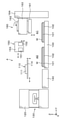
図6に示すように搬送ユニット110は、複数、例えば3つのアーム111~113を備えた多関節型のロボットである。3つのアーム111~113のうち、先端の第1のアーム111には、ウェハWを吸着保持する第2の保持部(基板保持部)としての搬送パッド114が取り付けられている。また、基端の第3のアーム113は、アーム111~113を鉛直方向に移動させる鉛直移動機構115に取り付けられている。
As shown in FIG. 6, the
搬送パッド114は、平面視において、ウェハWの径より長い径を備えた円形状を有する。その下面に複数の吸引口(図示せず)が形成され、各吸引口は真空引きする吸引機構(図示せず)に接続されている。これにより搬送パッド114は、ウェハWの加工面全面を吸着保持する。また、搬送パッド114は、第1のアーム111の先端部に支持されている。第1のアーム111の先端部には回転部111aが内蔵され、回転部111aは例えばモータなどを備えている。この回転部111aにより、搬送パッド114は回転自在に構成されている。
The
3つのアーム111~113は、それぞれ関節部112a、113aによって接続されている。すなわち、第1のアーム111の基端部と第2のアーム112の先端部は、当該第2のアーム112の先端部に内蔵された関節部112aで接続されている。関節部112aは例えばモータなどを備え、この関節部112aにより、第1のアーム111は基端部を中心に旋回自在に構成されている。同様に、第2のアーム112の基端部と第3のアーム113の先端部は、当該第3のアーム113の先端部に内蔵された関節部113aで接続されている。関節部113aも例えばモータなどを備え、この関節部113aにより、第2のアーム112は基端部を中心に旋回自在に構成されている。
The three
鉛直移動機構115は、鉛直方向に延伸するガイド115aを備え、第3のアーム113の基端部がガイド115aに取り付けられている。また、鉛直移動機構115には例えばモータなどを備えた駆動部(図示せず)が内蔵され、この駆動部により、第3のアーム113(アーム111~113)がガイド115aに沿って鉛直方向に移動自在に構成されている。
The
ここで、図7に示すように加工位置A1~A3では、研削ユニット160、170、180でウェハWの加工面を研削する際、水を使用する。また、受渡位置A0では、第3の洗浄ユニット150によりウェハWの加工面を粗洗浄する際、洗浄液を使用する。さらに、第2の洗浄ユニット140によりウェハWの非加工面を洗浄する際も、洗浄液を使用する。このため、これら水や洗浄液を使用する領域は、湿気を含むウェット環境領域R1(図7中の斜線領域)となる。また、ウェット環境領域R1では、研削ユニット160、170、180でウェハWの加工面を研削する際に、削り屑も発生する。
Here, as shown in FIG. 7, at the machining positions A1 to A3, water is used when grinding the machined surface of the wafer W by the grinding
そこで、鉛直移動機構115は、ウェット環境領域R1から隔離されたドライ環境領域R2(図7中の点線領域)に配置するのが好ましい。具体的にドライ環境領域R2は、後述する仕上研削ユニット180の支柱184のY軸負方向側の領域である。かかる場合、鉛直移動機構115の駆動部が湿気などにさらされず、当該駆動部を適切に動作させることができる。また、鉛直移動機構115のガイド115aは開口しているが、この摺動部であるガイド115aを保護するためのシール機構などが不要になり、装置構成を簡略化することも可能となる。さらに、ドライ環境領域R2は搬送ステーション6側にあるため、当該搬送ステーション6からのアクセスがしやすく、鉛直移動機構115のメンテナンスを容易に行うことができる。
Therefore, it is preferable to arrange the
なお、上述した回転部111aと関節部112a、113aはそれぞれ、アーム111~113に内蔵されてシールされているため、ウェット環境領域R1においても、さらなる保護は不要である。
Since the rotating
そして、かかる構成を備えた搬送ユニット110は、受渡位置A0、アライメントユニット120、第1の洗浄ユニット130、及び第2の洗浄ユニット140に対して、ウェハWを搬送できる。
Then, the
アライメントユニット120では、研削処理前のウェハWの水平方向の向きを調節する。図8に示すように、アライメントユニット120は処理容器121を有し、処理容器121の内部には基台122、スピンチャック123、及び検出部124が設けられている。スピンチャック123は、ウェハWを吸着保持し、回転機構(図示せず)によって回転自在に構成されている。検出部124は、例えばウェハWの外周部を撮像することでウェハWのノッチ部の位置を検出してもよいし、あるいはウェハWの周縁部にレーザ光を照射することでウェハWのノッチ部の位置を検出してもよい。そして、スピンチャック123に保持されたウェハWを回転させながら検出部124でウェハWのノッチ部の位置を検出することで、当該ノッチ部の位置を調節してウェハWの水平方向の向きを調節する。
The
なお、アライメントユニット120の下方には第1の洗浄ユニット130が配置されるが、第1の洗浄ユニット130は後述するようにスピンチャック133を備えるため、洗浄時にスピンチャック133が高速回転することで振動する。アライメントユニット120に振動が伝わるとウェハWの水平方向の向きを適切に調節できないため、処理容器121は第1の洗浄ユニット130から独立して支持されるのが好ましい。処理容器121の支持方法は任意であるが、例えばウェット環境領域R1に設けられた支持部材に支持されてもよいし、あるいは加工装置4の筐体(側壁)に支持されていてもよいし、加工装置4の天井面から吊下げ支持されていてもよい。
Although the
第1の洗浄ユニット130では、研削処理後のウェハWの加工面を洗浄し、より具体的にはスピン洗浄する。
In the
図9~図10に示すように、第1の洗浄ユニット130は矩形状の支持板131を有している。第1の洗浄ユニット130にはX軸正方向且つY軸正方向から、搬送ユニット110の第1のアーム111と搬送パッド114がアクセスする。このため、支持板131のX軸正方向且つY軸正方向はオープンにされている。
As shown in FIGS. 9 to 10, the
支持板131の周囲にはシャッタ132が設けられている。シャッタ132の上面と下面は開口している。シャッタ132は、昇降機構(図示せず)によって、支持板131の上方と下方に、鉛直方向に移動自在に構成されている。なお、シャッタ132の平面視における形状は、図示した矩形状に限定されず、支持板131の周囲を覆う形状、例えば円形状であってもよい。
A
図9(a)及び図10(a)に示すようにシャッタ132が支持板131の上方に位置する際、当該シャッタ132は、アライメントユニット120の処理容器121の底面と若干の隙間をあけて配置される。この隙間により、第1の洗浄ユニット130における洗浄処理時の振動が、アライメントユニット120に伝わるのを抑制できる。そして、支持板131、シャッタ132及び処理容器121で、処理空間Kが形成される。なお、処理容器121の底面には、シャッタ132の外方において、上述した処理容器121の底面とシャッタ132との隙間を覆うようにスカート121aが設けられている。このスカート121aにより、ウェハWの洗浄処理時に、洗浄液が外部に飛散することがない。
When the
一方、図9(b)及び図10(b)に示すようにシャッタ132が支持板131の下方に位置する際、処理空間Kが開放される。そして、搬送ユニット110によって処理空間KにウェハWが搬送される。また、開放された処理空間Kには、ウェハ搬送装置32の搬送パッド34が、搬送ユニット110とは異なる方向、すなわち搬送ステーション6側からアクセス可能である。
On the other hand, when the
処理空間Kの中央部には、ウェハWを保持して回転させるスピンチャック133が設けられている。スピンチャック133は、ウェハWを吸着保持する。スピンチャック133の下方には、例えばモータなどを備えた駆動部134が設けられている。スピンチャック133は、駆動部134により所定の速度に回転でき、また昇降自在になっている。スピンチャック133の周囲には、ウェハWから飛散又は落下する液体を受け止め、回収するカップ135が設けられている。
A
洗浄液ノズル136はウェハWの加工面に洗浄液、例えば純水を供給する。また、洗浄液ノズル136は、移動機構137により水平方向及び鉛直方向に移動自在に構成されている。そして、スピンチャック133に保持されたウェハWを回転させながら、洗浄液ノズル136からウェハWの加工面に洗浄液を供給する。そうすると、供給された洗浄液はウェハWの加工面上を拡散し、当該加工面が洗浄される。
The cleaning
第2の洗浄ユニット140では、研削処理後のウェハWであって搬送ユニット110の搬送パッド114に保持されたウェハWの非加工面を洗浄すると共に、搬送パッド114を洗浄する。図11に示すように、第2の洗浄ユニット140は処理容器141を有し、処理容器141の内部には洗浄液ノズルを有するスポンジ洗浄具142、エアノズル143、ストーン洗浄具144(砥石)、及びブラシ洗浄具145が設けられている。スポンジ洗浄具142、エアノズル143、ストーン洗浄具144、及びブラシ洗浄具145はそれぞれ、昇降機構(図示せず)によって鉛直方向に移動自在に構成されている。
In the
スポンジ洗浄具142は、例えばウェハWの径より長く延伸するスポンジを有し、スポンジには洗浄液、例えば純水を供給可能であり、当該非加工面、より詳細には非加工面に貼り付けられた保護テープを洗浄する。エアノズル143は、ウェハWの非加工面にエアを噴射して、当該非加工面を乾燥させる。これらスポンジ及び洗浄液による非加工面の洗浄と、エアによる非加工面の乾燥はそれぞれ、搬送パッド114でウェハWを保持した状態、且つ回転部111aによって搬送パッド114(ウェハW)を回転させながら行われる。これにより、ウェハWの非加工面全面が洗浄される。
The
ストーン洗浄具144とブラシ洗浄具145はそれぞれ、例えば搬送ユニット110の搬送パッド114におけるウェハWの吸着面の径より長く延伸し、当該吸着面に接触して洗浄する。そして、ストーン洗浄具144とブラシ洗浄具145による搬送パッド114の洗浄は、回転部111aによって搬送パッド114を回転させながら行われる。これにより搬送パッド114の全面が洗浄される。
Each of the
第3の洗浄ユニット150では、研削処理後のウェハWの加工面とチャック101を洗浄する。図3及び図4に示すように第3の洗浄ユニット150は、洗浄液ノズル151、ストーン洗浄具152(砥石)、及び移動機構153を有している。洗浄液ノズル151とストーン洗浄具152はそれぞれ、移動機構153によって、水平方向及び鉛直方向に移動自在に構成されている。
The
洗浄液ノズル151はウェハWの加工面に洗浄液、例えば純水を供給する。そして、チャック101に保持されたウェハWを回転させながら、洗浄液ノズル151からウェハWの加工面に洗浄液を供給する。そうすると、供給された洗浄液はウェハWの加工面上を拡散し、当該加工面が洗浄される。
The cleaning
ストーン洗浄具152は、チャック101の表面に接触して洗浄する。この際、ノズル(図示せず)からチャック101の表面に洗浄液、例えば純水を供給してもよい。
The
粗研削ユニット160では、ウェハWの加工面を粗研削する。粗研削ユニット160は環状形状の粗研削砥石161を有している。粗研削砥石161にはスピンドル162を介して駆動部163が設けられている。駆動部163は例えばモータ(図示せず)を内蔵し、粗研削砥石161を回転させると共に、支柱164に沿って鉛直方向及び水平方向(X軸方向)に移動させる。そして、チャック101に保持されたウェハWを粗研削砥石161の円弧の一部に当接させた状態で、チャック101と粗研削砥石161をそれぞれ回転させることによって、ウェハWの裏面を粗研削する。またこのとき、ウェハWの裏面に研削液、例えば水が供給される。
In the
中研削ユニット170では、ウェハWの裏面を中研削する。図3及び図5に示すように中研削ユニット170の構成は粗研削ユニット160の構成とほぼ同様であり、中研削砥石171スピンドル172、駆動部173、及び支柱174を有している。なお、中研削砥石171の粒度は、粗研削砥石161の粒度より小さい。そして、チャック101に保持されたウェハWの裏面に研削液を供給しながら、裏面を中研削砥石171の円弧の一部に当接させた状態で、チャック101と中研削砥石171をそれぞれ回転させることによってウェハWの裏面を研削する。
In the
仕上研削ユニット180では、ウェハWの裏面を仕上研削する。仕上研削ユニット180の構成は粗研削ユニット160、中研削ユニット170の構成とほぼ同様であり、仕上研削砥石181スピンドル182、駆動部183、及び支柱184を有している。なお、仕上研削砥石181の粒度は、中研削砥石171の粒度より小さい。そして、チャック101に保持されたウェハWの裏面に研削液を供給しながら、裏面を仕上研削砥石181の円弧の一部に当接させた状態で、チャック101と仕上研削砥石181をそれぞれ回転させることによってウェハWの裏面を研削する。
The
次に、以上のように構成された基板処理システム1を用いて行われるウェハ処理について説明する。
Next, the wafer processing performed by using the
先ず、複数のウェハWを収納したカセットCが、搬入ステーション2のカセット載置台10に載置される。カセットCには、保護テープが変形するのを抑制するため、当該保護テープが貼り付けられたウェハWの表面が上側を向くようにウェハWが収納されている。
First, the cassette C containing the plurality of wafers W is placed on the cassette mounting table 10 of the carry-in
次に、ウェハ搬送装置32の搬送フォーク33によりカセットC内のウェハWが取り出され、加工装置4に搬送される。この際、搬送フォーク33によりウェハWの加工面が上側に向くように、表裏面が反転される。
Next, the wafer W in the cassette C is taken out by the
加工装置4に搬送されたウェハWは、アライメントユニット120のスピンチャック123に受け渡される。そして、当該アライメントユニット120において、ウェハWの水平方向の向きが調節される(図12のステップS1)。
The wafer W conveyed to the
次に、図13(a)及び(b)に示すようにウェハWは搬送ユニット110によって、アライメントユニット120から受渡位置A0に搬送され、当該受渡位置A0のチャック101に受け渡される。その後、回転テーブル100を反時計回りに90度回転させ、チャック101を第1の加工位置A1に移動させる。そして、粗研削ユニット160によって、ウェハWの加工面が粗研削される(図12のステップS2)。
Next, as shown in FIGS. 13A and 13B, the wafer W is conveyed from the
なお、このステップS2においてウェハWがチャック101に保持される前に、チャック101は第3の洗浄ユニット150のストーン洗浄具152を用いて洗浄されている(図12のステップT1)。チャック101の洗浄は、ステップS2までの任意のタイミングで行われる。
Before the wafer W is held by the
次に、回転テーブル100を反時計回りに90度回転させ、チャック101を第2の加工位置A2に移動させる。そして、中研削ユニット170によって、ウェハWの裏面が中研削される(図12のステップS3)。
Next, the rotary table 100 is rotated 90 degrees counterclockwise to move the
次に、回転テーブル100を反時計回りに90度回転させ、チャック101を第3の加工位置A3に移動させる。そして、仕上研削ユニット180によって、ウェハWの裏面が仕上研削される(図12のステップS4)。
Next, the rotary table 100 is rotated 90 degrees counterclockwise to move the
次に、回転テーブル100を反時計回りに90度回転させ、又は回転テーブル100を時計回りに270度回転させて、チャック101を受渡位置A0に移動させる。そして、第3の洗浄ユニット150の洗浄液ノズル151を用いて、ウェハWの加工面が洗浄液によって粗洗浄される(図12のステップS5)。このステップS5では、加工面の汚れをある程度まで落とす洗浄が行われる。
Next, the rotary table 100 is rotated 90 degrees counterclockwise, or the rotary table 100 is rotated 270 degrees clockwise to move the
次に、図13(c)に示すようにウェハWは搬送ユニット110によって受渡位置A0から第2の洗浄ユニット140に搬送される。この際、ウェハWは薄化されているが、搬送パッド114はウェハWの加工面を全面で吸着保持する。そして、第2の洗浄ユニット140では、ウェハWが搬送パッド114に回転保持された状態で、スポンジ洗浄具142によってウェハWの非加工面が洗浄される(図12のステップS6)。その後さらに、ウェハWが搬送パッド114に回転保持された状態で、エアノズル143から非加工面にエアが噴射され、当該非加工面が乾燥される。
Next, as shown in FIG. 13 (c), the wafer W is transferred from the delivery position A0 to the
なお、このステップS6においてウェハWが搬送ユニット110によって搬送される前に、搬送ユニット110の搬送パッド114は、第2の洗浄ユニット140のストーン洗浄具144とブラシ洗浄具145を用いて洗浄されている(図12のステップT2)。ストーン洗浄具144とブラシ洗浄具145による搬送パッド114の洗浄は、回転部111aによって搬送パッド114を回転させながら行われる。また、搬送パッド114の洗浄は、ステップS6までの任意のタイミングで行われる。
Before the wafer W is transferred by the
次に、図13(d)に示すようにウェハWは搬送ユニット110によって、第2の洗浄ユニット140から第1の洗浄ユニット130に搬送される。ウェハWの搬送時、第1の洗浄ユニット130では、シャッタ132が支持板131の下方に位置し、処理空間Kが開放されている。その後、ウェハWがスピンチャック133に受け渡され、搬送ユニット110が退出すると、シャッタ132を昇降させて、当該シャッタ132を支持板131の上方に配置し、処理空間Kが形成される。その後、スピンチャック133に保持されたウェハWを回転させながら、洗浄液ノズル136からウェハWの加工面に洗浄液を供給し、当該加工面が仕上洗浄される(図12のステップS7)。このステップS7では、ウェハWの加工面が所望の清浄度まで洗浄し乾燥される。そして、ウェハWの加工面の仕上洗浄と乾燥が終了すると、シャッタ132を下降させて、当該シャッタ132を支持板131の下方に配置し、処理空間Kが開放される。
Next, as shown in FIG. 13D, the wafer W is transferred from the
その後、ウェハWはウェハ搬送装置32によって、第1の洗浄ユニット130から後処理装置5に搬送される。この際、ウェハWは薄化されているが、搬送パッド34はウェハWの加工面を全面で吸着保持する。そして、後処理装置5では、ウェハWをダイシングフレームに保持するマウント処理や、ウェハWに貼り付けられた保護テープを剥離する剥離処理などの後処理が行われる(図12のステップS8)。
After that, the wafer W is transferred from the
その後、すべての処理が施されたウェハWは、搬出ステーション3のカセット載置台20のカセットCに搬送される。こうして、基板処理システム1における一連のウェハ処理が終了する。
After that, the wafer W to which all the processing has been performed is transferred to the cassette C of the cassette mounting table 20 of the unloading
なお、一連のウェハ処理において加工装置4では、搬送ユニット110が動作を停止している際、当該搬送ユニット110の搬送パッド114は待機位置である、第2の洗浄ユニット140の上方に配置されている。この待機の際、搬送パッド114は回転テーブル100のチャック101(受渡位置A0及び加工位置A1~A3)より高い位置に配置されるのが好ましい。上述したステップS2~S4において研削ユニット160、170、180でウェハWの加工面を研削する際、削り屑が発生し、この削り屑を含む汚染空気がチャック101側から流れてくる。そこで、搬送パッド114の待機時に搬送パッド114をチャック101より高く配置することで、当該搬送パッド114が汚染空気によって汚染されるのを抑制することができる。
In the
以上の実施形態によれば、加工装置4において、搬送ユニット110は、3つのアーム111~113を備えた多関節型のロボットであり、各アーム111~113を独立して移動させることができるので、搬送パッド114が受渡位置A0、アライメントユニット120、第1の洗浄ユニット130、及び第2の洗浄ユニット140にアクセスすることができる。そして、このように1つの搬送ユニット110で、受渡位置A0及び各ユニット120、130、140にウェハWを搬送することができるので、当該搬送ユニット110の移動自由度を高くすることができる。さらに、ウェハWの搬送手段が1つであるため、加工装置4の装置構成を簡略化することもできる。したがって、ウェハ処理を効率よく行うことができる。
According to the above embodiment, in the
また、加工装置4において、受渡位置A0、第2の洗浄ユニット140、アライメントユニット120、及び第1の洗浄ユニット130は、Y軸方向に並べて配置されているので、搬送ユニット110のアクセス範囲を小さくすることができ、ウェハWを効率よく搬送することができる。
Further, in the
また、加工装置4においてアライメントユニット120と第1の洗浄ユニット130が積層されているので、加工装置4のフットプリントを小さくすることができる。その結果、加工装置4の設置自由度が向上する。また、このようにアライメントユニット120と第1の洗浄ユニット130を積層することで、これら各ユニット120、130のメンテナンスも容易に行うことができる。
Further, since the
さらに、アライメントユニット120と第1の洗浄ユニット130は上方からこの順で積層されており、すなわち液処理を行う第1の洗浄ユニット130がアライメントユニット120の下層に設けられている。かかる場合、第1の洗浄ユニット130における排液を第1の洗浄ユニット130の下部から容易に行うことができ、また第1の洗浄ユニット130で発生したパーティクルがアライメントユニット120に侵入することがない。但し、アライメントユニット120と第1の洗浄ユニット130の積層順はこれに限定されるものではない。
Further, the
また、本実施形態によれば、一の基板処理システム1において、一連の処理を複数のウェハWに対して連続して行うことができ、スループットを向上させることができる。
Further, according to the present embodiment, in one
なお、基板処理システム1の構成は、上記実施形態に限定されるものではない。例えば加工装置4において、アライメントユニット120と第1の洗浄ユニット130は積層されていたが、水平方向に並べて配置してもよい。但し、フットプリントを小さくする観点からは、積層した方が好ましい。また、第1の洗浄ユニット130は、加工装置4の外部、例えば加工装置4と後処理装置5の間に設けられてもよい。
The configuration of the
また、加工装置4において、第2の洗浄ユニット140は、アライメントユニット120及び第1の洗浄ユニット130と水平方向に並べて配置されていたが、これらアライメントユニット120と第1の洗浄ユニット130に積層されて設けられていてもよい。但し、搬送ユニット110の搬送パッド114には、必ず待機位置が必要になるため、その待機位置に第2の洗浄ユニット140を配置するのがレイアウトとしては効率がよい。
Further, in the
また、加工装置4において、搬送ユニット110の鉛直移動機構115はドライ環境領域R2に固定して設けられていたが、例えば図1のY軸方向に移動自在に構成されていてもよい。かかる場合、3つのアーム111~113のうち、いずれか1つのアームを省略してもよい。
Further, in the
また、基板処理システム1において、例えば加工装置4と後処理装置5の間に別のウェハ搬送装置が設けられていてもよい。このウェハ搬送装置は、例えば第1の洗浄ユニット130から後処理装置5にウェハWを搬送する。
Further, in the
また、基板処理システム1において、後処理装置5では、マウント処理や剥離処理が行われていたが、ウェハWに対するダイシング処理を行ってもよい。あるいは、基板処理システム1は、加工装置4と後処理装置5に加えて、ダイシング処理を行うダイシング装置を別途有していてもよい。このようなダイシング処理は、加工装置4における研削処理の前に行われてもよいし、研削処理の後で行われてもよい。さらに、基板処理システム1は後処理装置5を省略し、マウント処理や剥離処理、ダイシング処理を基板処理システム1の外部で行ってもよい。かかる場合、加工装置4で研削処理されたウェハWは、ウェハ搬送装置32の搬送パッド34により、第1の洗浄ユニット130からカセット載置台10に搬送される。
Further, in the
次に、上記実施形態の基板処理システム1の加工装置4における、搬送ユニット110の構成についてより詳細に説明する。すなわち、搬送ユニット110の搬送パッド114は、側面視において傾動自在にする場合と、この側面視における傾動を固定する場合を、切り替え自在に構成されている。搬送パッド114を傾動自在にする機構(以下、傾動機構という)と固定する機構(以下、固定機構という)は、それぞれ任意の構成を取り得るが、以下、その例を説明する。
Next, the configuration of the
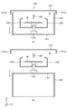
図14は、搬送パッド114の傾動機構200の構成の概略を示す説明図であり、(a)は平面図であり、(b)は側面図である。傾動機構200は、支持プレート201と付勢部202を有している。支持プレート201は円板形状を有し、搬送パッド114の上方において、当該搬送パッド114と同心円状に設けられている。また、支持プレート201は、第1のアーム111に支持されている。
14A and 14B are explanatory views showing an outline of the configuration of the
付勢部202は、支持プレート201に対して搬送パッド114を離間方向に付勢する。付勢部202は、支持プレート201の同一円周上を等間隔に複数、例えば3箇所に設けられている。この3つの付勢部202によって、搬送パッド114は、その鉛直方向の中心軸Cを中心に傾動可能に構成されている。
The urging
図15に示すように付勢部202は、ボルト203、ばね204、及びケース205を有している。ボルト203の先端部203aは、搬送パッド114に固定して設けられている。一方、ボルト203のボルトヘッド203bは、支持プレート201の上面側で上下動可能になっている。ボルト203の外周面には、ばね204が設けられている。ばね204は、ケース205に収容されている。かかる構成により、付勢部202は、支持プレート201に対して搬送パッド114を付勢できる。
As shown in FIG. 15, the urging
図16は、搬送パッド114の固定機構210の構成の概略を示す側面図である。固定機構210は、各付勢部202の上方に設けられている。固定機構210は、ロック部材211とシリンダ212を有している。ロック部材211はボルト203の上方において、鉛直方向に延伸して設けられている。シリンダ212はロック部材211を鉛直方向に移動させる。かかる構成により、固定機構210は、ロック部材211をボルト203のボルトヘッド203bに当接させることで、搬送パッド114の上下動を固定することができる。一方、固定機構210は、ロック部材211をボルト203と当接させないように上方に配置することで、搬送パッド114を上下動させることができる。
FIG. 16 is a side view showing an outline of the configuration of the
次に、以上の傾動機構200と固定機構210の動作について、上述した基板処理システム1におけるウェハ処理に即して説明する。なお、以下の説明において、搬送パッド114を傾動自在にさせるとは、固定機構210のロック部材211を傾動機構200のボルト203に当接させず、傾動機構200の機能によって、搬送パッド114の傾動がフリーな状態になっていることをいう。また、搬送パッド114の傾動を固定させるとは、ロック部材211をボルト203に当接させ、搬送パッド114の上下動がロックされている状態をいう。
Next, the operations of the
先ず、ステップS1においてアライメントユニット120でウェハWの水平方向の向きが調節された後、搬送ユニット110によってアライメントユニット120からウェハWを取り出す際には、搬送パッド114を傾動自在させる。これにより、例えばスピンチャック123に保持されたウェハWが水平でない場合でも、その傾きにそって搬送パッド114を傾動させることができ、ウェハWを適切に受け取ることができる。
First, after the horizontal orientation of the wafer W is adjusted by the
その後、搬送ユニット110によって、アライメントユニット120から受渡位置A0にウェハWを搬送する際には、搬送パッド114の傾動を固定する。これにより、搬送中にウェハWが不規則に上下動することを抑制することができる。
After that, when the wafer W is transferred from the
その後、搬送ユニット110によって、受渡位置A0のチャック101にウェハWを受け渡す際には、搬送パッド114を傾動自在させる。これにより、例えば図17に示すようにチャック101が平坦(水平)でない場合でも、その傾きにそって搬送パッド114を傾動させることができ、ウェハWを適切に受け渡すことができる。
After that, when the wafer W is delivered to the
その後、ステップS2~S5の研削処理が終了し、搬送ユニット110によって受渡位置A0のチャック101からウェハWを受け取る際には、搬送パッド114を傾動自在させる。
After that, when the grinding process in steps S2 to S5 is completed and the wafer W is received from the
その後、搬送ユニット110によって、受渡位置A0から第2の洗浄ユニット140にウェハWを搬送する際には、搬送パッド114の傾動を固定する。
After that, when the wafer W is transferred from the delivery position A0 to the
その後、ステップS6において、搬送パッド114に保持されたウェハWの非加工面を洗浄する際には、搬送パッド114の傾動を固定する。これにより、ウェハWが不規則に上下動しないので、非加工面を適切に洗浄することができる。
After that, in step S6, when cleaning the non-processed surface of the wafer W held by the
なお、このステップS6においてウェハWが搬送ユニット110によって搬送される前に、ステップT2において、第2の洗浄ユニット140のストーン洗浄具144とブラシ洗浄具145を用いて搬送パッド114が洗浄される。この搬送パッド114の洗浄の際には、図18に示すように搬送パッド114の傾動を固定する。これにより、搬送パッド114が不規則に上下動しないので、当該搬送パッド114を適切に洗浄することができる。
Before the wafer W is transported by the
その後、搬送ユニット110によって、第2の洗浄ユニット140から第1の洗浄ユニット130にウェハWを搬送する際には、搬送パッド114の傾動を固定する。
After that, when the wafer W is transferred from the
その後、搬送ユニット110によって、第1の洗浄ユニット130のスピンチャック133にウェハWを受け渡す際には、搬送パッド114を傾動自在させる。これにより、スピンチャック133が平坦(水平)でない場合でも、その傾きにそって搬送パッド114を傾動させることができ、ウェハWを適切に受け渡すことができる。
After that, when the wafer W is delivered to the
その後、ステップS8が行われるが、搬送ユニット110を用いない処理であるため、説明を省略する。
After that, step S8 is performed, but since it is a process that does not use the
以上の実施形態によれば、搬送ユニット110を用いたウェハWの受け渡し時(受け取り時)には、搬送パッド114を傾動自在にしている。このため、例えば受け渡す側のチャックが平坦(水平)でない場合でも、その傾きにそって搬送パッド114を傾動させることができ、ウェハWを適切に受け渡すことができる。
According to the above embodiment, when the wafer W is delivered (received) using the
一方、ウェハWの受け渡し以外の時、例えばウェハWの搬送時や洗浄時、搬送パッド114の洗浄時には、搬送パッド114の傾動を固定しているので、当該搬送や洗浄を適切に行うことができる。
On the other hand, since the tilt of the
このように、搬送パッド114の傾動と固定を切り替えることでウェハ処理を適切に行うことができる。
In this way, the wafer processing can be appropriately performed by switching between tilting and fixing of the
なお、以上の基板処理システム1は、搬送ユニット110の搬送パッド114に保持されたウェハWに対し、保護テープの厚みを計測する、計測部としての厚み計測器(図示せず)を有していてもよい。厚み計測器は公知の計測器を用いることができるが、例えば分光干渉計を用いることができる。
The
ここで、ウェハWに貼り付けられた保護テープは、テープ自体の厚みが面内でばらつく場合がある。また、保護テープをウェハWに貼り付ける際に張力が不均一になるために、保護テープの厚みが面内でばらつく場合もある。そして、このようにテープの厚みが不均一な状態で研削処理を行うと、当該研削がウェハ面内で不均一になってしまう。 Here, in the protective tape attached to the wafer W, the thickness of the tape itself may vary in the plane. Further, when the protective tape is attached to the wafer W, the tension becomes non-uniform, so that the thickness of the protective tape may vary in the plane. If the grinding process is performed in such a state that the thickness of the tape is non-uniform, the grinding becomes non-uniform in the wafer surface.
そこで、例えばステップS1においてアライメントユニット120でウェハWの水平方向の向きが調節された後、搬送ユニット110によって受渡位置A0にウェハWを搬送する際、搬送パッド114に保持されたウェハWに対し、厚み計測器によって保護テープの厚みを計測する。そして、ステップS2~S4の研削処理では、保護テープの厚みの計測結果に基づいて、ウェハWの加工面に対する研削ユニット160、170、180(研削砥石161、171、181)の当接の仕方を調節する。そうすると、ウェハ面内で均一な厚みにウェハWを研削して薄化することができる。
Therefore, for example, after the horizontal orientation of the wafer W is adjusted by the
このような保護テープの厚み計測を行う場合、搬送パッド114の傾動を固定する。これにより、保護テープの厚みを適切に計測することができる。なお、本実施形態は、保護テープに限らず他の保護部材、例えば塗布された保護剤や、ウェハWの表面(デバイスが形成された面)に支持基板などが貼り付けられた際に、当該他の保護部材の厚み計測を行う場合にも適用できる。
When measuring the thickness of such a protective tape, the tilt of the
なお、搬送パッド114の傾動機構と固定機構の構成は、上記実施形態に限定されるものではない。
The configuration of the tilting mechanism and the fixing mechanism of the
例えば図19に示すように固定機構220は、水平方向に延伸するロック部材221と、ロック部材221を水平方向に移動させるシリンダ222を有している。かかる構成により、固定機構220は、ロック部材221をボルト203に当接させることで、搬送パッド114の上下動を固定することができる。一方、固定機構220は、ロック部材221をボルト203と当接させないように側方に配置することで、搬送パッド114を上下動させることができる。
For example, as shown in FIG. 19, the
また、例えば図20に示すように固定機構230は、回転自在のロック部材231を有していてもよい。ロック部材231は、中心から径方向に延伸するアーム231aを3本有し、各アーム231aは傾動機構200のボルト203に対応するように設けられている。かかる構成により、固定機構230は、ロック部材231を回転させてアーム231aをボルト203に当接させることで、搬送パッド114の上下動を固定することができる。一方、固定機構230は、アーム231aをボルト203と当接させないように配置することで、搬送パッド114を上下動させることができる。
Further, for example, as shown in FIG. 20, the
また、例えば図21に示すように搬送ユニット110は、傾動機構と固定機構が複合した機構240(以下、複合機構240という)を有していてもよい。複合機構240は、搬送パッド114を支持する支持球体241と、支持球体241を真空引きして吸着する吸着体242とを有している。吸着体242の下面には、支持球体241の球形状に沿った湾曲部242aが形成されている。支持球体241は、湾曲部242aに沿って回転自在に構成されている。この支持球体241によって、搬送パッド114は、その鉛直方向の中心軸Cを中心に傾動可能に構成されている。また、湾曲部242aには複数の吸引口(図示せず)が形成され、各吸引口は真空引きする吸引機構(図示せず)に接続されている。
Further, for example, as shown in FIG. 21, the
かかる構成により、複合機構240は、吸着体242の湾曲部242aが支持球体241を真空引きして吸着保持する。これにより、支持球体241の回転が固定され、搬送パッド114の傾動を固定することができる。一方、吸着体242の湾曲部242aによる支持球体241の真空引きを停止することで、支持球体241は自由に回転することができる。そして、このように支持球体241が回転することで、搬送パッド114を、中心軸Cを中心に傾動させることができる。
With such a configuration, in the
なお、以上の実施形態の傾動機構200と固定機構210、220、230(複合機構240)は、搬送ユニット110の搬送パッド114に限らず、ウェハWを吸着保持して搬送するものであれば適用できる。例えば傾動機構200と固定機構210、220、230(複合機構240)は、ウェハ搬送装置32の搬送パッド34にも適用できる。
The
なお、以上の実施形態では、加工装置4においてウェハWの搬送手段は1つであったが、2つ設けられていてもよい。例えば1つ目の搬送手段は、研削処理前のウェハWを搬送し、アライメントユニット120と受渡位置A0の間でウェハWを搬送する。また、2つ目の搬送手段は、研削処理後のウェハWを搬送し、受渡位置A0、第1の洗浄ユニット130、及び第2の洗浄ユニット140の間でウェハWを搬送する。このように2つの搬送手段が設けられている場合でも、それぞれの搬送手段に対し、傾動機構200と固定機構210、220、230(複合機構240)を適用することができる。
In the above embodiment, the
以上、本発明の実施形態について説明したが、本発明はかかる例に限定されない。当業者であれば、請求の範囲に記載された技術的思想の範疇内において、各種の変更例または修正例に想到しうることは明らかであり、それらについても当然に本発明の技術的範囲に属するものと了解される。 Although the embodiments of the present invention have been described above, the present invention is not limited to such examples. It is clear that a person skilled in the art can come up with various modifications or modifications within the scope of the technical ideas described in the claims, and these are naturally within the technical scope of the present invention. It is understood that it belongs to.
例えば、以上の実施形態では、ウェハWの表面にはデバイスを保護するために保護テープが貼り付けられていたが、デバイスの保護部材はこれに限定されない。例えばウェハの表面には、塗布された保護剤や、支持ウェハやガラス基板などの支持基板が貼り合せられていてもよく、かかる場合でも本発明の一態様を適用することができる。 For example, in the above embodiment, a protective tape is attached to the surface of the wafer W to protect the device, but the protective member of the device is not limited to this. For example, a coated protective agent or a support substrate such as a support wafer or a glass substrate may be bonded to the surface of the wafer, and even in such a case, one aspect of the present invention can be applied.
1 基板処理システム
2 搬入ステーション
3 搬出ステーション
4 加工装置
5 後処理装置
6 搬送ステーション
10、20 カセット載置台
32 ウェハ搬送装置
33 搬送フォーク
34 搬送パッド
40 制御部
100 回転テーブル
101 チャック
110 搬送ユニット
111~113 アーム
111a 回転部
112a、113a 関節部
114 搬送パッド
115 鉛直移動機構
120 アライメントユニット
130 第1の洗浄ユニット
140 第2の洗浄ユニット
150 第3の洗浄ユニット
160 粗研削ユニット
170 中研削ユニット
180 仕上研削ユニット
200 傾動機構
210、220、230 固定機構
240 複合機構
A0 受渡位置
A1~A3 加工位置
R1 ウェット環境領域
R2 ドライ環境領域
W ウェハ1
Claims (17)
基板を保持する第1の保持部と、
前記第1の保持部に保持された基板の加工面を加工する加工部と、
前記加工部で加工された基板であって第2の保持部に保持された基板の加工面と反対側の非加工面を洗浄し、又は前記第2の保持部を洗浄する洗浄部と、
前記第2の保持部を備え、当該第2の保持部で基板を保持して搬送し、且つ前記第1の保持部に基板を受け渡す受渡位置と前記洗浄部に対し、基板を搬送する搬送部と、を有し、
前記搬送部は、
前記第2の保持部を側面視において傾動自在にする傾動機構と、
前記第2の保持部の側面視における傾動を固定する固定機構と、を有し、
前記受渡位置において前記搬送部が前記第1の保持部に基板を受け渡す際、前記第2の保持部は前記傾動機構によって傾動自在になっており、
前記洗浄部において基板の非加工面又は前記第2の保持部を洗浄する際、前記第2の保持部は前記固定機構によって固定されている。 It is a board processing system that processes boards.
The first holding part that holds the substrate and
A processing portion for processing the processed surface of the substrate held by the first holding portion, and a processing portion.
A cleaning unit that cleans the non-processed surface of the substrate processed by the processed portion and is held by the second holding portion on the side opposite to the processed surface of the substrate, or cleans the second holding portion.
The second holding portion is provided, and the substrate is held and conveyed by the second holding portion, and the substrate is conveyed to the delivery position where the substrate is delivered to the first holding portion and the cleaning portion. With a part,
The transport unit is
A tilting mechanism that makes the second holding portion tiltable in a side view,
It has a fixing mechanism for fixing the tilt of the second holding portion in a side view, and has a fixing mechanism.
When the transport unit delivers the substrate to the first holding unit at the delivery position, the second holding unit is tiltable by the tilting mechanism.
When cleaning the non-processed surface of the substrate or the second holding portion in the cleaning portion, the second holding portion is fixed by the fixing mechanism.
前記傾動機構は、前記第2の保持部の鉛直方向の中心軸を中心に傾動させる。 In the substrate processing system according to claim 1 ,
The tilting mechanism tilts the second holding portion about a central axis in the vertical direction.
前記搬送部で基板を搬送する際、前記第2の保持部は前記固定機構によって固定されている。 In the substrate processing system according to claim 1 or 2 .
When the substrate is conveyed by the conveying portion, the second holding portion is fixed by the fixing mechanism.
前記搬送部は、複数のアームと、前記複数のアームを接続する複数の関節部とを有し、
前記複数のアームのうち先端のアームは、前記第2の保持部を支持し、
前記関節部は前記アームを移動させる。 In the substrate processing system according to any one of claims 1 to 3 ,
The transport portion has a plurality of arms and a plurality of joint portions connecting the plurality of arms.
The arm at the tip of the plurality of arms supports the second holding portion.
The joint moves the arm.
前記搬送部は、前記先端のアームに設けられ、前記第2の保持部を回転させる回転部を有する。 In the substrate processing system according to claim 4 ,
The transport portion is provided on the arm at the tip and has a rotating portion for rotating the second holding portion.
前記搬送部は、前記複数のアームを鉛直方向に移動させる移動機構を有し、
前記移動機構は、前記加工部を支持する支持部を介して、前記加工部から隔離されて設けられている。 In the substrate processing system according to claim 4 or 5 .
The transport unit has a moving mechanism for moving the plurality of arms in the vertical direction.
The moving mechanism is provided so as to be isolated from the processed portion via a support portion that supports the processed portion.
前記第1の保持部に保持される前の基板の水平方向の向きを調節するアライメント部を有し、
前記搬送部は、前記アライメント部に対し基板を搬送し、
前記搬送部が前記アライメント部から基板を受け取る際、前記第2の保持部は前記傾動機構によって傾動自在になっている。 In the substrate processing system according to any one of claims 1 to 6 .
It has an alignment portion that adjusts the horizontal orientation of the substrate before being held by the first holding portion.
The transport unit transports the substrate to the alignment unit and transports the substrate.
When the transport unit receives the substrate from the alignment unit, the second holding unit is tiltable by the tilting mechanism.
前記加工部で加工された基板の加工面を洗浄する加工面洗浄部を有し、
前記搬送部は、前記加工面洗浄部に対し基板を搬送し、
前記搬送部が前記加工面洗浄部に基板を受け渡す際、前記第2の保持部は前記傾動機構によって傾動自在になっている。 In the substrate processing system according to any one of claims 1 to 7 .
It has a machined surface cleaning part that cleans the machined surface of the substrate machined by the machined part.
The transport section transports the substrate to the machined surface cleaning section.
When the transport unit delivers the substrate to the machined surface cleaning unit, the second holding unit is tiltable by the tilting mechanism.
基板の非加工面には、デバイスが形成されるとともに、当該非加工面に保護部材が設けられ、
前記第2の保持部に保持された基板の前記保護部材の厚みを計測する計測部を有し、
前記計測部において前記保護部材の厚みを計測する際、前記第2の保持部は前記固定機構によって固定されている。 In the substrate processing system according to any one of claims 1 to 8 ,
A device is formed on the non-processed surface of the substrate, and a protective member is provided on the non-processed surface.
It has a measuring unit for measuring the thickness of the protective member of the substrate held by the second holding unit.
When the thickness of the protective member is measured by the measuring unit, the second holding unit is fixed by the fixing mechanism.
前記第1の保持部を複数備え、前記受渡位置と前記加工部による加工が行われる加工位置との間で、複数の前記第1の保持部を回転させて移動させる回転テーブルを有する。 In the substrate processing system according to any one of claims 1 to 9 ,
It is provided with a plurality of the first holding portions, and has a rotary table for rotating and moving the plurality of the first holding portions between the delivery position and the machining position where the machining by the machining section is performed.
搬送部によって第1の保持部に基板を搬送する第1の搬送工程と、
その後、加工部によって、前記第1の保持部に保持された基板の加工面を加工する加工工程と、
その後、前記搬送部によって洗浄部に基板を搬送する第2の搬送工程と、
その後、前記洗浄部によって、前記搬送部の第2の保持部に保持された基板の加工面と反対側の非加工面を洗浄し、又は前記第2の保持部を洗浄する洗浄工程と、を有し、
前記搬送部は、
前記第2の保持部を側面視において傾動自在にする傾動機構と、
前記第2の保持部の側面視における傾動を固定する固定機構と、を有し、
前記第1の搬送工程において、前記搬送部が前記第1の保持部に基板を受け渡す際、前記第2の保持部は前記傾動機構によって傾動自在になっており、
前記洗浄工程において、基板の非加工面又は前記第2の保持部を洗浄する際、前記第2の保持部は前記固定機構によって固定されている。 It is a substrate processing method that processes a substrate.
The first transfer step of transporting the substrate to the first holding portion by the transport unit, and
After that, a processing step of processing the processed surface of the substrate held by the first holding portion by the processing portion, and
After that, a second transfer step of transporting the substrate to the cleaning section by the transport section, and
After that, the cleaning unit cleans the non-processed surface of the substrate held by the second holding portion of the transport unit on the opposite side to the processed surface, or cleans the second holding portion. Have and
The transport unit is
A tilting mechanism that makes the second holding portion tiltable in a side view,
It has a fixing mechanism for fixing the tilt of the second holding portion in a side view, and has a fixing mechanism.
In the first transfer step, when the transfer unit delivers the substrate to the first holding unit, the second holding unit is tiltable by the tilting mechanism.
In the cleaning step, when cleaning the non-processed surface of the substrate or the second holding portion, the second holding portion is fixed by the fixing mechanism.
前記傾動機構は、前記第2の保持部の鉛直方向の中心軸を中心に傾動させる。 In the substrate processing method according to claim 11 ,
The tilting mechanism tilts the second holding portion about a central axis in the vertical direction.
前記第1の搬送工程と前記第2の搬送工程のそれぞれにおいて、前記搬送部で基板を搬送する際、前記第2の保持部は前記固定機構によって固定されている。 In the substrate processing method according to claim 11 or 12 ,
In each of the first transfer step and the second transfer step, when the substrate is conveyed by the transfer section, the second holding section is fixed by the fixing mechanism.
前記第1の搬送工程の前に、アライメント部によって、基板の水平方向の向きを調節するアライメント工程を有し、
前記第1の搬送工程において、前記搬送部が前記アライメント部から基板を受け取る際、前記第2の保持部は前記傾動機構によって傾動自在になっている。 The substrate processing method according to any one of claims 11 to 13 .
Prior to the first transfer step, there is an alignment step of adjusting the horizontal orientation of the substrate by the alignment section.
In the first transfer step, when the transfer unit receives the substrate from the alignment unit, the second holding unit is tiltable by the tilting mechanism.
前記洗浄工程後、前記搬送部によって加工面洗浄部に基板を搬送する第3の搬送工程と、
その後、前記加工面洗浄部によって基板の加工面を洗浄する加工面洗浄工程と、を有し、
前記第3の搬送工程において、前記搬送部が前記加工面洗浄部に基板を受け渡す際、前記第2の保持部は前記傾動機構によって傾動自在になっている。 In the substrate processing method according to any one of claims 11 to 14 ,
After the cleaning step, a third transport step of transporting the substrate to the machined surface cleaning section by the transport section and
After that, it has a machined surface cleaning step of cleaning the machined surface of the substrate by the machined surface cleaning unit.
In the third transfer step, when the transfer unit delivers the substrate to the machined surface cleaning unit, the second holding unit is tiltable by the tilting mechanism.
基板の非加工面には、デバイスが形成されるとともに、当該非加工面に保護部材が設けられ、
前記第1の搬送工程において、計測部によって、前記第2の保持部に保持された基板の前記保護部材の厚みを計測し、当該計測する際、前記第2の保持部は前記固定機構によって固定されている。 The substrate processing method according to any one of claims 11 to 15 .
A device is formed on the non-processed surface of the substrate, and a protective member is provided on the non-processed surface.
In the first transfer step, the measuring unit measures the thickness of the protective member of the substrate held by the second holding unit, and when the measurement is performed, the second holding unit is fixed by the fixing mechanism. Has been done.
A readable computer storage that stores a program that operates on the computer of the control unit that controls the board processing system so that the board processing method according to any one of claims 11 to 16 is executed by the board processing system. Medium.
Applications Claiming Priority (3)
| Application Number | Priority Date | Filing Date | Title |
|---|---|---|---|
| JP2017224672 | 2017-11-22 | ||
| JP2017224672 | 2017-11-22 | ||
| PCT/JP2018/041637 WO2019102868A1 (en) | 2017-11-22 | 2018-11-09 | Substrate transfer device, substrate processing system, substrate processing method, and computer storage medium |
Publications (2)
| Publication Number | Publication Date |
|---|---|
| JPWO2019102868A1 JPWO2019102868A1 (en) | 2020-12-03 |
| JP7018452B2 true JP7018452B2 (en) | 2022-02-10 |
Family
ID=66630981
Family Applications (1)
| Application Number | Title | Priority Date | Filing Date |
|---|---|---|---|
| JP2019555254A Active JP7018452B2 (en) | 2017-11-22 | 2018-11-09 | Board processing system, board processing method and computer storage medium |
Country Status (6)
| Country | Link |
|---|---|
| US (1) | US11120985B2 (en) |
| JP (1) | JP7018452B2 (en) |
| KR (1) | KR102581315B1 (en) |
| CN (1) | CN111386598B (en) |
| TW (1) | TWI803535B (en) |
| WO (1) | WO2019102868A1 (en) |
Families Citing this family (3)
| Publication number | Priority date | Publication date | Assignee | Title |
|---|---|---|---|---|
| CN112261785B (en) * | 2020-10-19 | 2021-12-17 | 嘉兴桀华电子科技有限公司 | Integrated circuit board processing device |
| JP2022152042A (en) * | 2021-03-29 | 2022-10-12 | 株式会社ディスコ | Polishing device |
| CN117049125B (en) * | 2023-10-11 | 2023-12-26 | 合肥铠柏科技有限公司 | Sample conveyer capable of self-adapting to angle error of sample rack |
Citations (11)
| Publication number | Priority date | Publication date | Assignee | Title |
|---|---|---|---|---|
| JP2003092274A (en) | 2001-09-19 | 2003-03-28 | Nikon Corp | Apparatus and method for working, method of manufacturing semiconductor device using the apparatus and semiconductor device manufactured by the method |
| JP2004202690A (en) | 2001-02-07 | 2004-07-22 | Nissan Motor Co Ltd | Sucking and holding device |
| JP2002307356A5 (en) | 2001-12-12 | 2005-03-17 | ||
| JP2006019600A (en) | 2004-07-05 | 2006-01-19 | Lintec Corp | Transfer device |
| JP2007136659A (en) | 2005-11-21 | 2007-06-07 | Nissan Motor Co Ltd | Method, system, and apparatus for transferring workpiece |
| JP2008147275A (en) | 2006-12-07 | 2008-06-26 | Disco Abrasive Syst Ltd | Conveyor for wafer |
| JP2011018802A (en) | 2009-07-09 | 2011-01-27 | Disco Abrasive Syst Ltd | Grinding apparatus |
| JP2011513669A (en) | 2008-03-17 | 2011-04-28 | コリア ニューマチック システム カンパニー,リミテッド | Vacuum pad device |
| JP2015020242A (en) | 2013-07-19 | 2015-02-02 | 株式会社荏原製作所 | Polishing device, and polishing condition monitoring method |
| JP2016132047A (en) | 2015-01-16 | 2016-07-25 | 株式会社ディスコ | Griding method for workpiece |
| JP2017005070A (en) | 2015-06-09 | 2017-01-05 | 株式会社ディスコ | Carrier device |
Family Cites Families (27)
| Publication number | Priority date | Publication date | Assignee | Title |
|---|---|---|---|---|
| JPS571116Y2 (en) * | 1978-01-31 | 1982-01-08 | ||
| JPS5867685U (en) * | 1981-10-29 | 1983-05-09 | 日本電気ホームエレクトロニクス株式会社 | Suction hand structure |
| FR2557004B1 (en) * | 1983-12-23 | 1986-05-09 | Renault | HEAD WITH SIX AXES OF CORRECTION OF MOVEMENTS |
| US4684113A (en) * | 1984-09-28 | 1987-08-04 | The Boeing Company | Universal holding fixture |
| JPS62102985A (en) | 1985-10-30 | 1987-05-13 | 日立金属株式会社 | Gripper for robot |
| JP3197019B2 (en) * | 1991-03-18 | 2001-08-13 | 株式会社ブリヂストン | Adsorption method for belt-shaped members |
| US5457868A (en) * | 1991-03-26 | 1995-10-17 | Gfm Gesellschaft Fur Fertigungstechnik Und Maschinenbau Aktiengesellschaft | Work supporting method using a deck for use in machine tools, particularly in cutting machines |
| DE4408537A1 (en) * | 1994-03-14 | 1995-09-21 | Leybold Ag | Device for the transport of substrates |
| JP3894514B2 (en) * | 1997-04-04 | 2007-03-22 | 株式会社ディスコ | Polishing equipment |
| JP3389456B2 (en) * | 1997-06-09 | 2003-03-24 | 株式会社安川電機 | Industrial robot |
| DE19817777C1 (en) * | 1998-04-21 | 1999-09-09 | Schmalz J Gmbh | Suction handling head for flat panels |
| US6189876B1 (en) * | 1998-05-05 | 2001-02-20 | Mcms, Inc. | Method and apparatus for leveling the upper surface of a PCB |
| JP4106450B2 (en) * | 2001-02-07 | 2008-06-25 | 日産自動車株式会社 | Adsorption holding device |
| JP4464113B2 (en) * | 2003-11-27 | 2010-05-19 | 株式会社ディスコ | Wafer processing equipment |
| US7195535B1 (en) * | 2004-07-22 | 2007-03-27 | Applied Materials, Inc. | Metrology for chemical mechanical polishing |
| US7975998B2 (en) * | 2006-04-03 | 2011-07-12 | Midaco Corporation | Pallet changer and system and method for using the same |
| JP4655074B2 (en) * | 2007-07-27 | 2011-03-23 | トヨタ自動車株式会社 | Work transfer device and work installation method |
| JP2010058213A (en) * | 2008-09-03 | 2010-03-18 | Central Motor Co Ltd | Vacuum pad device |
| KR101289366B1 (en) * | 2008-09-12 | 2013-07-29 | 가부시키가이샤 다이후쿠 | Substrate transporting facility |
| JP5287741B2 (en) * | 2010-01-21 | 2013-09-11 | 富士通株式会社 | Component mounter and component mounting method |
| JP5619559B2 (en) * | 2010-10-12 | 2014-11-05 | 株式会社ディスコ | Processing equipment |
| JP5323867B2 (en) * | 2011-01-19 | 2013-10-23 | 東京エレクトロン株式会社 | Substrate inversion apparatus, substrate inversion method, peeling system, program, and computer storage medium |
| JP6037685B2 (en) | 2012-07-03 | 2016-12-07 | 株式会社ディスコ | Grinding equipment |
| TWI675721B (en) * | 2013-07-11 | 2019-11-01 | 日商荏原製作所股份有限公司 | Polishing apparatus and polished-state monitoring method |
| JP6496535B2 (en) * | 2014-12-02 | 2019-04-03 | リコーエレメックス株式会社 | Holding device |
| CN104900554B (en) * | 2015-04-15 | 2017-10-17 | 四川虹视显示技术有限公司 | A kind of oled substrate metal level detection and distributor |
| CN206255626U (en) * | 2016-07-25 | 2017-06-16 | K.C.科技股份有限公司 | Base plate transfer device and the base plate processing system comprising it |
-
2018
- 2018-11-09 JP JP2019555254A patent/JP7018452B2/en active Active
- 2018-11-09 US US16/765,902 patent/US11120985B2/en active Active
- 2018-11-09 CN CN201880074073.1A patent/CN111386598B/en active Active
- 2018-11-09 KR KR1020207017460A patent/KR102581315B1/en active IP Right Grant
- 2018-11-09 WO PCT/JP2018/041637 patent/WO2019102868A1/en active Application Filing
- 2018-11-19 TW TW107140949A patent/TWI803535B/en active
Patent Citations (11)
| Publication number | Priority date | Publication date | Assignee | Title |
|---|---|---|---|---|
| JP2004202690A (en) | 2001-02-07 | 2004-07-22 | Nissan Motor Co Ltd | Sucking and holding device |
| JP2003092274A (en) | 2001-09-19 | 2003-03-28 | Nikon Corp | Apparatus and method for working, method of manufacturing semiconductor device using the apparatus and semiconductor device manufactured by the method |
| JP2002307356A5 (en) | 2001-12-12 | 2005-03-17 | ||
| JP2006019600A (en) | 2004-07-05 | 2006-01-19 | Lintec Corp | Transfer device |
| JP2007136659A (en) | 2005-11-21 | 2007-06-07 | Nissan Motor Co Ltd | Method, system, and apparatus for transferring workpiece |
| JP2008147275A (en) | 2006-12-07 | 2008-06-26 | Disco Abrasive Syst Ltd | Conveyor for wafer |
| JP2011513669A (en) | 2008-03-17 | 2011-04-28 | コリア ニューマチック システム カンパニー,リミテッド | Vacuum pad device |
| JP2011018802A (en) | 2009-07-09 | 2011-01-27 | Disco Abrasive Syst Ltd | Grinding apparatus |
| JP2015020242A (en) | 2013-07-19 | 2015-02-02 | 株式会社荏原製作所 | Polishing device, and polishing condition monitoring method |
| JP2016132047A (en) | 2015-01-16 | 2016-07-25 | 株式会社ディスコ | Griding method for workpiece |
| JP2017005070A (en) | 2015-06-09 | 2017-01-05 | 株式会社ディスコ | Carrier device |
Also Published As
| Publication number | Publication date |
|---|---|
| TW201926524A (en) | 2019-07-01 |
| KR20200087832A (en) | 2020-07-21 |
| US11120985B2 (en) | 2021-09-14 |
| TWI803535B (en) | 2023-06-01 |
| US20200306925A1 (en) | 2020-10-01 |
| JPWO2019102868A1 (en) | 2020-12-03 |
| KR102581315B1 (en) | 2023-09-22 |
| CN111386598B (en) | 2023-10-20 |
| CN111386598A (en) | 2020-07-07 |
| WO2019102868A1 (en) | 2019-05-31 |
Similar Documents
| Publication | Publication Date | Title |
|---|---|---|
| JP7018452B2 (en) | Board processing system, board processing method and computer storage medium | |
| JP6752367B2 (en) | Board processing system, board processing method and computer storage medium | |
| JP6937370B2 (en) | Grinding equipment, grinding methods and computer storage media | |
| TW201620676A (en) | Processing module, processing apparatus, and processing method | |
| JP6877585B2 (en) | Board processing system, board processing method and computer storage medium | |
| JP7002874B2 (en) | Board processing system | |
| JPWO2019013042A1 (en) | Substrate processing system, substrate processing method, and computer storage medium | |
| JP7071818B2 (en) | Board processing system | |
| KR20150120869A (en) | Substrate processing apparatus | |
| JP2006054388A (en) | Workpiece-conveying equipment, spinner-cleaning equipment, grinder, workpiece-conveying method | |
| JP6995143B2 (en) | Board processing system, board processing method and computer storage medium | |
| TWI811489B (en) | Wafer fabrication device | |
| JP6990720B2 (en) | Cleaning equipment, cleaning methods and computer storage media | |
| JP6968201B2 (en) | Board processing system, board processing method and computer storage medium | |
| JP6983311B2 (en) | Board processing system and board processing method | |
| JP3227448U (en) | Substrate grinding system | |
| JP5689367B2 (en) | Substrate transport method and substrate transport machine | |
| WO2022113795A1 (en) | Substrate processing system and substrate processing method | |
| WO2022054605A1 (en) | Thickness measurement device and thickness measurement method | |
| TWI837277B (en) | Processing device and processing method | |
| JP2008130576A (en) | Wafer carrying method and processing apparatus | |
| JP2022046137A (en) | Substrate treatment method and substrate treatment system | |
| JP2019114684A (en) | Substrate processing system, substrate processing method, program, and computer storage medium | |
| JP2020183000A (en) | Processing device |
Legal Events
| Date | Code | Title | Description |
|---|---|---|---|
| A521 | Request for written amendment filed |
Free format text: JAPANESE INTERMEDIATE CODE: A523 Effective date: 20200512 |
|
| A621 | Written request for application examination |
Free format text: JAPANESE INTERMEDIATE CODE: A621 Effective date: 20200512 |
|
| A131 | Notification of reasons for refusal |
Free format text: JAPANESE INTERMEDIATE CODE: A131 Effective date: 20210803 |
|
| A521 | Request for written amendment filed |
Free format text: JAPANESE INTERMEDIATE CODE: A523 Effective date: 20211001 |
|
| TRDD | Decision of grant or rejection written | ||
| A01 | Written decision to grant a patent or to grant a registration (utility model) |
Free format text: JAPANESE INTERMEDIATE CODE: A01 Effective date: 20220104 |
|
| A61 | First payment of annual fees (during grant procedure) |
Free format text: JAPANESE INTERMEDIATE CODE: A61 Effective date: 20220131 |
|
| R150 | Certificate of patent or registration of utility model |
Ref document number: 7018452 Country of ref document: JP Free format text: JAPANESE INTERMEDIATE CODE: R150 |