JP7017993B2 - Power converter and bus bar - Google Patents
Power converter and bus bar Download PDFInfo
- Publication number
- JP7017993B2 JP7017993B2 JP2018142853A JP2018142853A JP7017993B2 JP 7017993 B2 JP7017993 B2 JP 7017993B2 JP 2018142853 A JP2018142853 A JP 2018142853A JP 2018142853 A JP2018142853 A JP 2018142853A JP 7017993 B2 JP7017993 B2 JP 7017993B2
- Authority
- JP
- Japan
- Prior art keywords
- bus bar
- electronic component
- conversion device
- moment
- inertia
- Prior art date
- Legal status (The legal status is an assumption and is not a legal conclusion. Google has not performed a legal analysis and makes no representation as to the accuracy of the status listed.)
- Active
Links
Images


Landscapes
- Inverter Devices (AREA)
Description
本発明は、電力変換装置及びバスバに関するものである。 The present invention relates to a power converter and a bus bar.
電力変換装置においては、電子部品同士を接続するためにバスバを用いる場合がある。例えば、特許文献1には、一端が中間部材を介してはんだにより下部電極板と接続され、他端が外部端子とボルトにより締結された上部電極板(バスバ)を備える半導体装置が開示されている。
In a power conversion device, a bus bar may be used to connect electronic components to each other. For example,
特許文献1の上部電極板においては、一方がはんだ付けされているために、一端側の高さと他端側の高さとが必ずしも一致せず、固定された両端において応力集中が発生する可能性がある。また、同様に、両端がボルトにより対象物と締結されるバスバにおいても、バスバが取り付けられる対象物の位置によっては、一端側の高さと他端側の高さとが一致しない場合があり、その際もバスバの変形により応力集中する部分が出来る為、振動による破断の虞がある。
In the upper electrode plate of
本発明は、上述する問題点に鑑みてなされたもので、バスバの局所的な応力集中を抑制させることを目的とする。 The present invention has been made in view of the above-mentioned problems, and an object of the present invention is to suppress local stress concentration of the bus bar.
上記目的を達成するために、本発明では、電力変換装置に係る第1の手段として、パワー半導体素子を含む電子部品と、前記電子部品に接続されるバスバとを備える電力変換装置であって、前記バスバは、前記電子部品と締結される両端部の断面二次モーメントが大きく、両端部の間の中央部の断面二次モーメントが小さくなるように形状設定される、という構成を採用する。 In order to achieve the above object, in the present invention, as a first means relating to the power conversion device, the power conversion device includes an electronic component including a power semiconductor element and a bus bar connected to the electronic component. The bus bar adopts a configuration in which the shape is set so that the moment of inertia of area at both ends to be fastened to the electronic component is large and the moment of inertia of area at the center between both ends is small.
電力変換装置に係る第2の手段として、前記バスバは、前記両端部から前記中央部に向かうにつれて幅が減少するように形状設定されている、という構成を採用する。 As a second means relating to the power conversion device, the bus bar is shaped so that the width decreases from both end portions toward the center portion.
電力変換装置に係る第3の手段として、前記バスバは、平面から突出したビード形状を有し、前記両端部から前記中央部に向かうにつれて前記ビード形状の高さが減少するように形状設定されている、という構成を採用する。 As a third means according to the power conversion device, the bus bar has a bead shape protruding from a plane, and the shape is set so that the height of the bead shape decreases from both ends thereof toward the central portion. Adopt the configuration that there is.
電力変換装置に係る第4の手段として、前記バスバは、前記両端部から前記中央部に向かうにつれて板厚が薄くなるように形状設定されている、という構成を採用する。 As a fourth means relating to the power conversion device, the bus bar adopts a configuration in which the plate thickness is set so as to become thinner from both ends thereof toward the central portion.
電力変換装置に係る第5の手段として、前記電子部品が配置されると共に前記バスバの前記両端部を囲う壁部を有するケースを備え、前記バスバは、前記壁部に当接する位置決め部を有する、という構成を採用する。 As a fifth means according to the power conversion device, the electronic component is arranged and a case having a wall portion surrounding the both ends of the bus bar is provided, and the bus bar has a positioning portion that abuts on the wall portion. The configuration is adopted.
バスバに係る第1の手段として、両端において電子部品と接続されるバスバであって、電子部品と締結される両端部の断面二次モーメントが大きく、両端部に挟まれる中央部の断面二次モーメントが小さくなるように形状設定される、という構成を採用する。 As the first means related to the bus bar, it is a bus bar connected to an electronic component at both ends, and the moment of inertia of area at both ends to be fastened to the electronic component is large, and the moment of inertia of area at the center sandwiched between both ends is large. The shape is set so that
本発明によれば、バスバは、中央部の断面二次モーメントが小さいため、中央部が弾性変形し、両端部は変形しない。したがって、バスバにおいて、両端の高さ位置が異なる場合にも、両端に応力集中が発生せず、従来形状と比較してバスバにかかる局所的な応力を分散させることが可能であり、結果、バスバの破断を抑制できる。 According to the present invention, since the moment of inertia of area at the central portion of the bass bar is small, the central portion is elastically deformed and both ends are not deformed. Therefore, even when the height positions of both ends of the bus bar are different, stress concentration does not occur at both ends, and it is possible to disperse the local stress applied to the bus bar as compared with the conventional shape, and as a result, the bus bar. Can suppress the breakage of.
以下、図面を参照して、本発明に係る電力変換装置の一実施形態について説明する。
本実施形態に係る電力変換装置1は、ハイブリッド車や電気自動車等、モータを動力源として走行する車両に搭載される。
Hereinafter, an embodiment of the power conversion device according to the present invention will be described with reference to the drawings.
The
[第1実施形態]
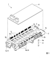
本実施形態に係る電力変換装置1は、不図示のモータを駆動するパワーモジュールを備える装置であり、モータ及び車載バッテリと電気的に接続されている。電力変換装置1は、図1に示すように、パワーモジュールケース2と、パワーモジュール3と、複数の電極接続端子4と、信号端子5と、回路基板6と、冷却器7と、バスバ8と、コンデンサ(図1には不図示)とを備えている。また、電力変換装置1は、パワーモジュールケース2、パワーモジュール3、複数の電極接続端子4、信号端子5、回路基板6及びコンデンサを収容するケース(不図示)を備えている。パワーモジュール3とモータ(不図示)とは、電極接続端子4及びバスバ8を介して接続されている。
[First Embodiment]
The
パワーモジュールケース2は、パワーモジュール3を収容する樹脂製のケースである。また、パワーモジュールケース2は、上面2aから立設される壁部2bを有しており、壁部2bにより区切られた各空間にパワーモジュール3が配置されている。また、パワーモジュールケース2の上面2a縁部には、上面2aから上方へと突出した端子台2cが形成されている。また、パワーモジュールケース2の下側には、冷却器7が設けられている。また、パワーモジュールケース2には、バスバ8を固定するためのボルト孔が形成されており、該ボルト孔にはインサートナットNが挿入されている。
The
パワーモジュール3は、パワー半導体素子を含む電力変換回路である。このようなパワーモジュール3は、信号端子5とワイヤボンディング(不図示)により電気的に接続されている。
The
電極接続端子4は、パワーモジュール3と電力線とを接続する金属板(例えば銅板)である。本実施形態においては、3つの電極接続端子4が1組として設けられている。電極接続端子4の一端は、パワーモジュールケース2内においてパワーモジュール3と接続される。電極接続端子4の他端は、パワーモジュールケース2の側面に設けられる接続端子4aとされる。本実施形態においては、3つの接続端子4aが1組として、側面に所定の間隔を開けて配列される。このような電極接続端子4は、図1及び図2(b)に示すように、中央部にボルトBが挿通する開口が設けられている。
The
なお、電力変換装置1の設置姿勢は特に限定されない。ただし、以下の説明においては、説明の便宜上、接続端子4aの配列方向を電力変換装置1の左右方向と、側面に平行かつ接続端子4aの配列方向に直交する方向(図1の上下方向)を電力変換装置1の上下方向と定義する。
The installation posture of the
信号端子5は、図1及び2に示すように、パワーモジュールケース2に一部が埋設されて固定された金属部品である。信号端子5は、一端5aが端子台2cから突出して設けられた細長状とされ、他端5bが上面2a上に露出している。すなわち、信号端子5は、中央部が屈曲されると共にパワーモジュールケース2にモールドされて固定されている。信号端子5の一端5aは、先細形状とされ、電磁シールド6及び絶縁シート7からも露出しており、回路基板6と電気的に接続されている。また、信号端子5の他端5bは、上面2aより露出する面を有しており、該面において、パワー半導体素子にボンディングワイヤ(信号配線)により接続されている。これにより、信号端子5は、パワー半導体素子と回路基板6とを電気的に接続している。
As shown in FIGS. 1 and 2, the signal terminal 5 is a metal component partially embedded and fixed in the
回路基板6は、パワーモジュールケース2の上面に固定配置されている。回路基板6には、不図示の制御回路が実装される。回路基板6(制御回路)は、所定の通信ケーブルなどを介してモータECU等の上位制御装置と接続されており、上位制御装置から入力される制御指令に基づいて車両に搭載される昇降圧コンバータ、インバータ等を制御する。
The
冷却器7は、冷媒入口7a及び冷媒出口7bを有する扁平な容器状とされている。冷却器7の内部には、冷媒が流通し、パワー半導体素子3a等から伝えられる熱を冷媒へと伝達することにより、パワー半導体素子3a等を冷却している。
The
バスバ8は、図2(a)に示すように、両端部にボルト締結孔8aが形成されている細長形状の金属板(例えば銅板)である。バスバ8は、図2(b)に示すように一端がパワーモジュール3の接続端子4aに対してボルトBにより締結され、他端がコンデンサ(電子部品)の接続端子Cに対してボルトBで接続されることにより、電気的に接続されている。すなわち、バスバ8は、パワーモジュール3とコンデンサとを電気的に接続している。バスバ8は、ボルト締結孔8aの近傍において短手方向に突出した突出部8bを有し、突出部8bから中央部、すなわち2つのボルト締結孔8aの中間点に向かって、徐々に幅が減少するように形状設定されている。すなわち、バスバ8は、端部の幅が太く設定されると共に中央部の幅が狭くなっていることで、端部の断面積が大きく、中央部の断面積が小さい形状とされている。なお、バスバ8において最も幅が狭くなる部位においても、電気的に必要とされる幅を満たすように設定されている。
As shown in FIG. 2A, the
なお、コンデンサは、電力変換装置1のケース内において、パワーモジュール3よりも下側に設けられており、バスバ8によってパワーモジュールと電気的に接続されている。
The capacitor is provided below the
このような電力変換装置1は、バッテリから供給される電力を、直流から交流へと変換すると共にモータへと伝える装置であり、モータへの供給電力を制御する。
Such a
このようなバスバ8において、接続端子4a及びコンデンサの接続端子CとボルトBにより締結される際に、接続端子4aとコンデンサの接続端子Cとが高さ方向(図2(b)における上下方向)における位置が異なる場合がある。このとき、バスバ8は、中央部の断面二次モーメントが小さいため、中央部が弾性変形し、ボルト締結孔8aを含む端部は変形しない。したがって、バスバ8において、両端の高さ位置が異なる場合にも、両端に応力集中が発生せず、従来形状と比較してバスバ8の応力を分散させることが可能である。また、振動が発生した場合にも、中央部へと力を逃がすことが可能であり、両端部に応力が集中しないため、バスバ8の破断を抑制させることが可能である。
In such a
[第2実施形態]
続いて、上記第1実施形態の変形例を第2実施形態として説明する。なお、上記第1実施形態と同一の構成については符号を同一とし、説明を省略する。
本実施形態においては、図3(a)に示すように、パワーモジュールケース2は、バスバ8が設置される位置において、ボルト孔を囲う円弧状に立設される絶縁壁部2dを備えている。絶縁壁部2dは、パワーモジュールケース2と共に樹脂により構成され、バスバ8の先端が内側に配置されることで、バスバ8からその他のパワーモジュールケース2に配置される部材へと通電することを防止している。バスバ8は、先端が絶縁壁部2dの円弧の内側に設けられると共に突出部8bが絶縁壁部2dの端部と接触するように配置される。
[Second Embodiment]
Subsequently, a modification of the first embodiment will be described as a second embodiment. The same components as those in the first embodiment will have the same reference numerals, and the description thereof will be omitted.
In the present embodiment, as shown in FIG. 3A, the
このような配置とすることにより、突出部が絶縁壁部2dの端部に当接することで、バスバ8がボルト締結孔8aを中心として回転することがない。したがって、バスバ8の位置決めが容易であり、バスバ8を締結する際に、バスバ8がボルト締結孔8aの周方向において固定された状態となるため端部に応力が集中せず、両端部と中央部とにおいて発生する応力を均一とすることが可能である。また、本実施形態に係るバスバ8は、突出部8bがバスバ8端部の最大幅部であるため、殆どサイズ・重量の増加無しに装置に対して適用可能である。
With such an arrangement, the protruding portion abuts on the end portion of the insulating
[第3実施形態]
続いて、上記第1実施形態の変形例を第3実施形態として説明する。なお、上記第1実施形態と同一の構成については符号を同一とし、説明を省略する。
[Third Embodiment]
Subsequently, a modification of the first embodiment will be described as a third embodiment. The same components as those in the first embodiment will have the same reference numerals, and the description thereof will be omitted.
本実施形態において、電力変換装置1は、バスバ8に代えて図3(b)に示すバスバ8Aを備えている。バスバ8Aは、屈曲されることにより幅方向における中間点が頂点となるように突出したビード形状8cを有している。ビード形状8cは、両端部のボルト締結孔8aの間の部位において長手方向に沿って形成されている。また、ビード形状8cは、バスバ8Aにおける長手方向の両端部から中央部に向けて頂点の高さが徐々に低くなるように形状設定されている。なお、このようなビード形状8cは、パンチ加工等により形成される。
In the present embodiment, the
このようなバスバ8Aによれば、ビード形状8cの頂点高さが相対的に高い両端部側において断面二次モーメントが大きく、ビード形状8cの頂点高さが相対的に低い中央部において断面二次モーメントが小さい。したがって、中央部が変形することで応力を逃がすことが可能であり、バスバ8Aの端部に応力が集中することなく、従来形状と比較してバスバ8Aの応力を分散させることが可能である。
According to such a
[第4実施形態]
続いて、上記第1実施形態の変形例を第4実施形態として説明する。なお、上記第1実施形態と同一の構成については符号を同一とし、説明を省略する。
[Fourth Embodiment]
Subsequently, a modified example of the first embodiment will be described as a fourth embodiment. The same components as those in the first embodiment will have the same reference numerals, and the description thereof will be omitted.
本実施形態において、電力変換装置1は、バスバ8に代えて図3(c)に示すバスバ8Bを備えている。バスバ8Bは、両端のボルト締結孔8aの間において、板厚(長手方向及び幅方向に対して垂直な方向の厚さ)が徐々に中央部に向けて薄くなるように形状設定されている。
In the present embodiment, the
このようなバスバ8Bによれば、バスバ8Bの厚さが相対的に厚い両端部側において断面二次モーメントが大きく、バスバ8Bの厚さが相対的に薄い中央部において断面二次モーメントが小さい。したがって、中央部が変形することで応力を逃がすことが可能であり、バスバ8Bの端部に応力が集中することなく、従来形状と比較してバスバ8Bの応力を分散させることが可能である。
According to such a
以上、図面を参照しながら本発明の好適な実施形態について説明したが、本発明は上記実施形態に限定されるものではない。上述した実施形態において示した各構成部材の諸形状や組み合わせ等は一例であって、本発明の趣旨から逸脱しない範囲において設計要求等に基づき種々変更可能である。 Although the preferred embodiment of the present invention has been described above with reference to the drawings, the present invention is not limited to the above embodiment. The various shapes and combinations of the constituent members shown in the above-described embodiment are examples, and can be variously changed based on design requirements and the like without departing from the spirit of the present invention.
上記実施形態においては、バスバ8は、コンデンサの接続端子Cと接続端子4aとを接続するものとしたが、本発明はこれに限定されない。バスバ8は、電力変換装置1において、他の電子部品同士を接続するものとしてもよい。また、バスバ8は、外部装置とパワーモジュール3または回路基板6とを接続するものとしてもよい。
In the above embodiment, the
1……電力変換装置
3……パワーモジュール
8……バスバ
8a……ボルト締結孔
8A……バスバ
8b……突出部
8B……バスバ
8c……ビード形状
1 ……
Claims (4)
前記バスバは、前記電子部品と締結される両端部の断面二次モーメントが大きく、両端部の間の中央部の断面二次モーメントが小さくなるように形状設定され、前記両端部から前記中央部に向かうにつれて幅が減少するように形状設定されていることを特徴とする電力変換装置。 A power conversion device including an electronic component including a power semiconductor element and a bus bar connected to the electronic component.
The shape of the bus bar is set so that the moment of inertia of area at both ends to be fastened to the electronic component is large and the moment of inertia of area at the center between both ends is small, and the moment of inertia is set from both ends to the center. A power conversion device characterized in that the shape is set so that the width decreases as it goes toward it .
前記バスバは、前記電子部品と締結される両端部の断面二次モーメントが大きく、両端部の間の中央部の断面二次モーメントが小さくなるように形状設定され、前記バスバの主面から突出したビード形状を有し、前記両端部から前記中央部に向かうにつれて前記ビード形状の高さが減少するように形状設定されていることを特徴とする電力変換装置。 A power conversion device including an electronic component including a power semiconductor element and a bus bar connected to the electronic component.
The shape of the bus bar is set so that the moment of inertia of area at both ends to be fastened to the electronic component is large and the moment of inertia of area at the center between the ends is small, and the bus bar protrudes from the main surface of the bus bar. A power conversion device having a bead shape and having a shape set so that the height of the bead shape decreases toward the central portion from both ends thereof .
前記バスバは、前記電子部品と締結される両端部の断面二次モーメントが大きく、両端部の間の中央部の断面二次モーメントが小さくなるように形状設定され、前記両端部から前記中央部に向かうにつれて板厚が薄くなるように形状設定されていることを特徴とする電力変換装置。 A power conversion device including an electronic component including a power semiconductor element and a bus bar connected to the electronic component.
The shape of the bus bar is set so that the moment of inertia of area at both ends to be fastened to the electronic component is large and the moment of inertia of area at the center between both ends is small, and the moment of inertia is set from both ends to the center. A power conversion device characterized in that the shape is set so that the plate thickness becomes thinner as it goes toward it .
前記バスバは、前記壁部に当接する位置決め部を有することを特徴とする請求項1~3のいずれか一項に記載の電力変換装置。
It is provided with a case in which the electronic component is arranged and has a wall portion surrounding the both ends of the bus bar.
The power conversion device according to any one of claims 1 to 3 , wherein the bus bar has a positioning portion that abuts on the wall portion .
Priority Applications (1)
| Application Number | Priority Date | Filing Date | Title |
|---|---|---|---|
| JP2018142853A JP7017993B2 (en) | 2018-07-30 | 2018-07-30 | Power converter and bus bar |
Applications Claiming Priority (1)
| Application Number | Priority Date | Filing Date | Title |
|---|---|---|---|
| JP2018142853A JP7017993B2 (en) | 2018-07-30 | 2018-07-30 | Power converter and bus bar |
Publications (2)
| Publication Number | Publication Date |
|---|---|
| JP2020022235A JP2020022235A (en) | 2020-02-06 |
| JP7017993B2 true JP7017993B2 (en) | 2022-02-09 |
Family
ID=69588810
Family Applications (1)
| Application Number | Title | Priority Date | Filing Date |
|---|---|---|---|
| JP2018142853A Active JP7017993B2 (en) | 2018-07-30 | 2018-07-30 | Power converter and bus bar |
Country Status (1)
| Country | Link |
|---|---|
| JP (1) | JP7017993B2 (en) |
Families Citing this family (1)
| Publication number | Priority date | Publication date | Assignee | Title |
|---|---|---|---|---|
| JP7189190B2 (en) * | 2020-10-21 | 2022-12-13 | 矢崎総業株式会社 | Bus bar and resin body |
Citations (2)
| Publication number | Priority date | Publication date | Assignee | Title |
|---|---|---|---|---|
| JP2009130963A (en) | 2007-11-20 | 2009-06-11 | Mitsubishi Heavy Ind Ltd | Bus bar structure and inverter-integrated electric compressor |
| JP2017127152A (en) | 2016-01-15 | 2017-07-20 | 住友重機械工業株式会社 | Power conversion apparatus, shovel using the same, and laminated bus bar |
Family Cites Families (2)
| Publication number | Priority date | Publication date | Assignee | Title |
|---|---|---|---|---|
| JP2013073929A (en) * | 2011-09-29 | 2013-04-22 | Gs Yuasa Corp | Battery pack |
| JP2018014824A (en) * | 2016-07-20 | 2018-01-25 | 株式会社ケーヒン | Current sensor unit |
-
2018
- 2018-07-30 JP JP2018142853A patent/JP7017993B2/en active Active
Patent Citations (2)
| Publication number | Priority date | Publication date | Assignee | Title |
|---|---|---|---|---|
| JP2009130963A (en) | 2007-11-20 | 2009-06-11 | Mitsubishi Heavy Ind Ltd | Bus bar structure and inverter-integrated electric compressor |
| JP2017127152A (en) | 2016-01-15 | 2017-07-20 | 住友重機械工業株式会社 | Power conversion apparatus, shovel using the same, and laminated bus bar |
Also Published As
| Publication number | Publication date |
|---|---|
| JP2020022235A (en) | 2020-02-06 |
Similar Documents
| Publication | Publication Date | Title |
|---|---|---|
| CN101505041B (en) | Electric connection box | |
| JP5714716B2 (en) | Power control device | |
| US10756012B2 (en) | Circuit assembly | |
| JP4523632B2 (en) | Semiconductor device | |
| CN110915312B (en) | Circuit structure and electrical connection box | |
| US20220263305A1 (en) | Circuit structure | |
| CN103517606B (en) | Electronic installation | |
| JP2012070509A (en) | Electronic control device | |
| JP2016220277A (en) | Electric connection box | |
| JP2005295724A (en) | Electric connection box | |
| JP6510316B2 (en) | Electrical connection box | |
| JP7017993B2 (en) | Power converter and bus bar | |
| US10389099B2 (en) | Circuit assembly | |
| JP5790079B2 (en) | Discharge resistance fixed structure | |
| CN110301166A (en) | Electronic-component module and method for manufacturing electronic-component module | |
| JP7022028B2 (en) | Power converter | |
| JP7007131B2 (en) | Heat dissipation structure in circuit board equipment | |
| JP5376209B2 (en) | Circuit structure | |
| JP2013065695A (en) | Motor control device | |
| JP4349289B2 (en) | Electrical junction box | |
| JP2017135185A (en) | Electronic control unit | |
| WO2020017468A1 (en) | Circuit board | |
| WO2020017471A1 (en) | Circuit board | |
| JP2005168218A (en) | Electrical junction box | |
| JP5531565B2 (en) | Electrical junction box and method of manufacturing electrical junction box |
Legal Events
| Date | Code | Title | Description |
|---|---|---|---|
| A621 | Written request for application examination |
Free format text: JAPANESE INTERMEDIATE CODE: A621 Effective date: 20201208 |
|
| A711 | Notification of change in applicant |
Free format text: JAPANESE INTERMEDIATE CODE: A712 Effective date: 20210226 |
|
| RD04 | Notification of resignation of power of attorney |
Free format text: JAPANESE INTERMEDIATE CODE: A7424 Effective date: 20210408 |
|
| A977 | Report on retrieval |
Free format text: JAPANESE INTERMEDIATE CODE: A971007 Effective date: 20211025 |
|
| A131 | Notification of reasons for refusal |
Free format text: JAPANESE INTERMEDIATE CODE: A131 Effective date: 20211102 |
|
| A521 | Request for written amendment filed |
Free format text: JAPANESE INTERMEDIATE CODE: A523 Effective date: 20211221 |
|
| TRDD | Decision of grant or rejection written | ||
| A01 | Written decision to grant a patent or to grant a registration (utility model) |
Free format text: JAPANESE INTERMEDIATE CODE: A01 Effective date: 20220118 |
|
| A61 | First payment of annual fees (during grant procedure) |
Free format text: JAPANESE INTERMEDIATE CODE: A61 Effective date: 20220128 |
|
| R150 | Certificate of patent or registration of utility model |
Ref document number: 7017993 Country of ref document: JP Free format text: JAPANESE INTERMEDIATE CODE: R150 |
|
| R250 | Receipt of annual fees |
Free format text: JAPANESE INTERMEDIATE CODE: R250 |
|
| R250 | Receipt of annual fees |
Free format text: JAPANESE INTERMEDIATE CODE: R250 |