JP6996461B2 - Semiconductor device - Google Patents
Semiconductor device Download PDFInfo
- Publication number
- JP6996461B2 JP6996461B2 JP2018169878A JP2018169878A JP6996461B2 JP 6996461 B2 JP6996461 B2 JP 6996461B2 JP 2018169878 A JP2018169878 A JP 2018169878A JP 2018169878 A JP2018169878 A JP 2018169878A JP 6996461 B2 JP6996461 B2 JP 6996461B2
- Authority
- JP
- Japan
- Prior art keywords
- trench
- igbt
- fwd
- region
- pitch
- Prior art date
- Legal status (The legal status is an assumption and is not a legal conclusion. Google has not performed a legal analysis and makes no representation as to the accuracy of the status listed.)
- Active
Links
Images


Classifications
-
- H—ELECTRICITY
- H10—SEMICONDUCTOR DEVICES; ELECTRIC SOLID-STATE DEVICES NOT OTHERWISE PROVIDED FOR
- H10D—INORGANIC ELECTRIC SEMICONDUCTOR DEVICES
- H10D8/00—Diodes
- H10D8/422—PN diodes having the PN junctions in mesas
-
- H—ELECTRICITY
- H10—SEMICONDUCTOR DEVICES; ELECTRIC SOLID-STATE DEVICES NOT OTHERWISE PROVIDED FOR
- H10D—INORGANIC ELECTRIC SEMICONDUCTOR DEVICES
- H10D12/00—Bipolar devices controlled by the field effect, e.g. insulated-gate bipolar transistors [IGBT]
- H10D12/411—Insulated-gate bipolar transistors [IGBT]
- H10D12/441—Vertical IGBTs
- H10D12/461—Vertical IGBTs having non-planar surfaces, e.g. having trenches, recesses or pillars in the surfaces of the emitter, base or collector regions
- H10D12/481—Vertical IGBTs having non-planar surfaces, e.g. having trenches, recesses or pillars in the surfaces of the emitter, base or collector regions having gate structures on slanted surfaces, on vertical surfaces, or in grooves, e.g. trench gate IGBTs
-
- H—ELECTRICITY
- H10—SEMICONDUCTOR DEVICES; ELECTRIC SOLID-STATE DEVICES NOT OTHERWISE PROVIDED FOR
- H10D—INORGANIC ELECTRIC SEMICONDUCTOR DEVICES
- H10D30/00—Field-effect transistors [FET]
- H10D30/60—Insulated-gate field-effect transistors [IGFET]
-
- H—ELECTRICITY
- H10—SEMICONDUCTOR DEVICES; ELECTRIC SOLID-STATE DEVICES NOT OTHERWISE PROVIDED FOR
- H10D—INORGANIC ELECTRIC SEMICONDUCTOR DEVICES
- H10D62/00—Semiconductor bodies, or regions thereof, of devices having potential barriers
- H10D62/10—Shapes, relative sizes or dispositions of the regions of the semiconductor bodies; Shapes of the semiconductor bodies
- H10D62/124—Shapes, relative sizes or dispositions of the regions of semiconductor bodies or of junctions between the regions
- H10D62/126—Top-view geometrical layouts of the regions or the junctions
- H10D62/127—Top-view geometrical layouts of the regions or the junctions of cellular field-effect devices, e.g. multicellular DMOS transistors or IGBTs
-
- H—ELECTRICITY
- H10—SEMICONDUCTOR DEVICES; ELECTRIC SOLID-STATE DEVICES NOT OTHERWISE PROVIDED FOR
- H10D—INORGANIC ELECTRIC SEMICONDUCTOR DEVICES
- H10D62/00—Semiconductor bodies, or regions thereof, of devices having potential barriers
- H10D62/10—Shapes, relative sizes or dispositions of the regions of the semiconductor bodies; Shapes of the semiconductor bodies
- H10D62/129—Cathode regions of diodes
-
- H—ELECTRICITY
- H10—SEMICONDUCTOR DEVICES; ELECTRIC SOLID-STATE DEVICES NOT OTHERWISE PROVIDED FOR
- H10D—INORGANIC ELECTRIC SEMICONDUCTOR DEVICES
- H10D62/00—Semiconductor bodies, or regions thereof, of devices having potential barriers
- H10D62/10—Shapes, relative sizes or dispositions of the regions of the semiconductor bodies; Shapes of the semiconductor bodies
- H10D62/13—Semiconductor regions connected to electrodes carrying current to be rectified, amplified or switched, e.g. source or drain regions
- H10D62/141—Anode or cathode regions of thyristors; Collector or emitter regions of gated bipolar-mode devices, e.g. of IGBTs
- H10D62/142—Anode regions of thyristors or collector regions of gated bipolar-mode devices
-
- H—ELECTRICITY
- H10—SEMICONDUCTOR DEVICES; ELECTRIC SOLID-STATE DEVICES NOT OTHERWISE PROVIDED FOR
- H10D—INORGANIC ELECTRIC SEMICONDUCTOR DEVICES
- H10D64/00—Electrodes of devices having potential barriers
- H10D64/111—Field plates
- H10D64/117—Recessed field plates, e.g. trench field plates or buried field plates
-
- H—ELECTRICITY
- H10—SEMICONDUCTOR DEVICES; ELECTRIC SOLID-STATE DEVICES NOT OTHERWISE PROVIDED FOR
- H10D—INORGANIC ELECTRIC SEMICONDUCTOR DEVICES
- H10D8/00—Diodes
-
- H—ELECTRICITY
- H10—SEMICONDUCTOR DEVICES; ELECTRIC SOLID-STATE DEVICES NOT OTHERWISE PROVIDED FOR
- H10D—INORGANIC ELECTRIC SEMICONDUCTOR DEVICES
- H10D8/00—Diodes
- H10D8/60—Schottky-barrier diodes
-
- H—ELECTRICITY
- H10—SEMICONDUCTOR DEVICES; ELECTRIC SOLID-STATE DEVICES NOT OTHERWISE PROVIDED FOR
- H10D—INORGANIC ELECTRIC SEMICONDUCTOR DEVICES
- H10D84/00—Integrated devices formed in or on semiconductor substrates that comprise only semiconducting layers, e.g. on Si wafers or on GaAs-on-Si wafers
- H10D84/01—Manufacture or treatment
- H10D84/0123—Integrating together multiple components covered by H10D12/00 or H10D30/00, e.g. integrating multiple IGBTs
- H10D84/0126—Integrating together multiple components covered by H10D12/00 or H10D30/00, e.g. integrating multiple IGBTs the components including insulated gates, e.g. IGFETs
-
- H—ELECTRICITY
- H10—SEMICONDUCTOR DEVICES; ELECTRIC SOLID-STATE DEVICES NOT OTHERWISE PROVIDED FOR
- H10D—INORGANIC ELECTRIC SEMICONDUCTOR DEVICES
- H10D84/00—Integrated devices formed in or on semiconductor substrates that comprise only semiconducting layers, e.g. on Si wafers or on GaAs-on-Si wafers
- H10D84/01—Manufacture or treatment
- H10D84/02—Manufacture or treatment characterised by using material-based technologies
- H10D84/03—Manufacture or treatment characterised by using material-based technologies using Group IV technology, e.g. silicon technology or silicon-carbide [SiC] technology
- H10D84/038—Manufacture or treatment characterised by using material-based technologies using Group IV technology, e.g. silicon technology or silicon-carbide [SiC] technology using silicon technology, e.g. SiGe
-
- H—ELECTRICITY
- H10—SEMICONDUCTOR DEVICES; ELECTRIC SOLID-STATE DEVICES NOT OTHERWISE PROVIDED FOR
- H10W—GENERIC PACKAGES, INTERCONNECTIONS, CONNECTORS OR OTHER CONSTRUCTIONAL DETAILS OF DEVICES COVERED BY CLASS H10
- H10W10/00—Isolation regions in semiconductor bodies between components of integrated devices
- H10W10/01—Manufacture or treatment
-
- H—ELECTRICITY
- H10—SEMICONDUCTOR DEVICES; ELECTRIC SOLID-STATE DEVICES NOT OTHERWISE PROVIDED FOR
- H10D—INORGANIC ELECTRIC SEMICONDUCTOR DEVICES
- H10D62/00—Semiconductor bodies, or regions thereof, of devices having potential barriers
- H10D62/10—Shapes, relative sizes or dispositions of the regions of the semiconductor bodies; Shapes of the semiconductor bodies
- H10D62/102—Constructional design considerations for preventing surface leakage or controlling electric field concentration
- H10D62/103—Constructional design considerations for preventing surface leakage or controlling electric field concentration for increasing or controlling the breakdown voltage of reverse-biased devices
- H10D62/105—Constructional design considerations for preventing surface leakage or controlling electric field concentration for increasing or controlling the breakdown voltage of reverse-biased devices by having particular doping profiles, shapes or arrangements of PN junctions; by having supplementary regions, e.g. junction termination extension [JTE]
- H10D62/106—Constructional design considerations for preventing surface leakage or controlling electric field concentration for increasing or controlling the breakdown voltage of reverse-biased devices by having particular doping profiles, shapes or arrangements of PN junctions; by having supplementary regions, e.g. junction termination extension [JTE] having supplementary regions doped oppositely to or in rectifying contact with regions of the semiconductor bodies, e.g. guard rings with PN or Schottky junctions
- H10D62/107—Buried supplementary regions, e.g. buried guard rings
-
- H—ELECTRICITY
- H10—SEMICONDUCTOR DEVICES; ELECTRIC SOLID-STATE DEVICES NOT OTHERWISE PROVIDED FOR
- H10D—INORGANIC ELECTRIC SEMICONDUCTOR DEVICES
- H10D62/00—Semiconductor bodies, or regions thereof, of devices having potential barriers
- H10D62/10—Shapes, relative sizes or dispositions of the regions of the semiconductor bodies; Shapes of the semiconductor bodies
- H10D62/128—Anode regions of diodes
Landscapes
- Electrodes Of Semiconductors (AREA)
- Metal-Oxide And Bipolar Metal-Oxide Semiconductor Integrated Circuits (AREA)
Description
本発明は、絶縁ゲート構造を有する絶縁ゲートバイポーラトランジスタ(以下では、IGBTという)素子とフリーホイールダイオード(以下では、FWDという)素子とが共通の半導体基板に形成された半導体装置に関するものである。 The present invention relates to a semiconductor device in which an insulated gate bipolar transistor (hereinafter referred to as an IGBT) element having an insulated gate structure and a free wheel diode (hereinafter referred to as FWD) element are formed on a common semiconductor substrate.
従来より、インバータ等に使用されるスイッチング素子として、例えば、IGBT素子を有するIGBT領域と、FWD素子を有するFWD領域とが共通の半導体基板に形成された半導体装置が提案されている(例えば、特許文献1参照)。 Conventionally, as a switching element used in an inverter or the like, for example, a semiconductor device in which an IGBT region having an IGBT element and an FWD region having an FWD element are formed on a common semiconductor substrate has been proposed (for example, a patent). See Document 1).
具体的には、この半導体装置では、N-型のドリフト層を構成する半導体基板の表層部にベース層が形成され、ベース層を貫通するように複数のトレンチが形成されている。そして、各トレンチには、ゲート絶縁膜およびゲート電極が順に形成されている。これにより、トレンチゲート構造が構成されている。また、ベース層の表層部には、トレンチに接するようにN+型のエミッタ領域が形成されている。半導体基板の裏面側には、P+型のコレクタ層およびN+型のカソード層が形成されている。 Specifically, in this semiconductor device, a base layer is formed on the surface layer portion of the semiconductor substrate constituting the N - type drift layer, and a plurality of trenches are formed so as to penetrate the base layer. A gate insulating film and a gate electrode are sequentially formed in each trench. This constitutes a trench gate structure. Further, an N + type emitter region is formed on the surface layer portion of the base layer so as to be in contact with the trench. A P + type collector layer and an N + type cathode layer are formed on the back surface side of the semiconductor substrate.
そして、半導体基板の表面側となる一面側には、ベース層およびエミッタ領域と電気的に接続される上部電極が形成されている。半導体基板の裏面側となる他面側には、コレクタ層およびカソード層と電気的に接続される下部電極が形成されている。 An upper electrode electrically connected to the base layer and the emitter region is formed on one surface side of the semiconductor substrate. A lower electrode electrically connected to the collector layer and the cathode layer is formed on the other surface side, which is the back surface side of the semiconductor substrate.
このような半導体装置では、半導体基板の裏面側にコレクタ層が形成されている領域がIGBT領域とされ、カソード層が形成されている領域がFWD領域とされる。なお、FWD領域では、上記構成とされていることにより、N型のカソード層およびドリフト層と、P型のベース層とによってPN接合を有するFWD素子が構成される。 In such a semiconductor device, the region in which the collector layer is formed on the back surface side of the semiconductor substrate is referred to as an IGBT region, and the region in which the cathode layer is formed is referred to as an FWD region. In the FWD region, the FWD element having a PN junction is configured by the N-type cathode layer and the drift layer and the P-type base layer due to the above configuration.
また、上記半導体装置では、IGBT領域に形成されるトレンチは、一方向に延設された第1トレンチと、隣合う第1トレンチを繋ぐように一方向と交差する方向に延設された第2トレンチとが連通されて格子状とされている。 Further, in the above semiconductor device, the trench formed in the IGBT region is a second extending in a direction intersecting one direction so as to connect the first trench extending in one direction and the adjacent first trench. It communicates with the trench to form a grid pattern.
このような半導体装置では、トレンチが格子状とされているため、例えば、トレンチがストライプ状とされている場合と比較して、等電位線がトレンチを避けるように形成されることで等電位線が半導体基板の一面側に入り込み難くなる。このため、IGBT領域では、電界集中が発生し難くなり、耐圧の向上を図ることができる。 In such a semiconductor device, since the trenches are in a grid pattern, for example, the equipotential lines are formed so as to avoid the trenches as compared with the case where the trenches are striped. Is difficult to get into one side of the semiconductor substrate. Therefore, in the IGBT region, electric field concentration is less likely to occur, and the withstand voltage can be improved.
ところで、上記のような半導体装置では、さらにFWD領域での耐圧を向上させることも望まれている。このため、FWD領域においても、トレンチを格子状とすることが考えられる。しかしながら、FWD領域のトレンチを格子状としてIGBT領域のトレンチとFWD領域のトレンチとを繋いでしまうと、IGBT領域に配置されたゲート電極とFWD領域に配置されたゲート電極とが電気的に接続されてしまう。この場合、FWD領域に配置されたゲート電極がIGBT領域に配置されたゲート電極と同電位となるため、FWD素子の特性が変動してしまう可能性がある。 By the way, in the above-mentioned semiconductor device, it is also desired to further improve the withstand voltage in the FWD region. Therefore, even in the FWD region, it is conceivable that the trenches are in a grid pattern. However, if the trenches in the FWD region are arranged in a grid pattern and the trenches in the IGBT region and the trenches in the FWD region are connected, the gate electrode arranged in the IGBT region and the gate electrode arranged in the FWD region are electrically connected. Will end up. In this case, since the gate electrode arranged in the FWD region has the same potential as the gate electrode arranged in the IGBT region, the characteristics of the FWD element may fluctuate.
したがって、FWD領域での耐圧を向上させつつ、FWD素子の特性が変動することを抑制するためには、例えば、FWD領域のトレンチを格子状としつつ、FWD領域のトレンチをIGBT領域のトレンチと連通させないようにすることが考えられる。しかしながら、この構成では、各領域に形成された格子状トレンチの間の領域では、トレンチ密度が低くなる可能性があり、当該領域の耐圧が低くなる可能性がある。 Therefore, in order to improve the withstand voltage in the FWD region and suppress the fluctuation of the characteristics of the FWD element, for example, the trench in the FWD region is communicated with the trench in the IGBT region while the trench in the FWD region is formed in a grid pattern. It is conceivable not to let it. However, in this configuration, the trench density may be low in the region between the grid-like trenches formed in each region, and the withstand voltage of the region may be low.
本発明は上記点に鑑み、耐圧を向上できる半導体装置を提供することを目的とする。 In view of the above points, it is an object of the present invention to provide a semiconductor device capable of improving withstand voltage.
上記目的を達成するための請求項1、3、4、7、10では、IGBT領域(1)とFWD領域(2)とが共通の半導体基板(10)に形成されている半導体装置であって、第1導電型のドリフト層(11)と、ドリフト層上に形成された第2導電型のベース層(12)と、ベース層を貫通するトレンチ(13a、13b)の壁面に形成されたゲート絶縁膜(14)と、ゲート絶縁膜上に形成されたゲート電極(15a、15b)と、を有する複数のトレンチゲート構造と、ベース層の表層部であって、IGBT領域に形成されたトレンチと接するように形成された第1導電型のエミッタ領域(19)と、ドリフト層を挟んでベース層側と反対側に形成された第2導電型のコレクタ層(16)と、ドリフト層を挟んでベース層と反対側に形成されると共にコレクタ層と隣接する第1導電型のカソード層(17)と、ベース層およびエミッタ領域と電気的に接続される第1電極(22)と、コレクタ層およびカソード層と電気的に接続される第2電極(18)と、を備えている。コレクタ層上の領域がIGBT領域とされ、カソード層上の領域がFWD領域とされており、トレンチは、IGBT領域に形成されるゲート電極としての第1ゲート電極(14a)が配置されるIGBT用トレンチ(13a)と、FWD領域に形成され、第1ゲート電極とは別に制御されるゲート電極としての第2ゲート電極(14b)が配置されるFWD用トレンチ(13b)であり、IGBT用トレンチは、半導体基板の面方向における一方向に沿った第1方向に延設されたIGBT用第1トレンチ(131a)と、半導体基板の面方向における第1方向と交差する第2方向に延設されたIGBT用第2トレンチ(132a)とが連通された格子状とされており、FWD用トレンチは、第1方向に延設されたFWD用第1トレンチ(131b)と、第2方向に延設されたFWD用第2トレンチ(132b)とが連通された格子状とされている。
In
そして、請求項1では、IGBT用第1トレンチのうちの最もFWD用トレンチ側に位置するトレンチ(133a)の中心と、FWD用第1トレンチのうちの最もIGBT用トレンチ側に位置するトレンチ(133b)の中心との間を分離セル領域(3a)とすると共に分離セル領域における第2方向の距離を分離セルピッチ(W1)とし、隣合うIGBT用第1トレンチ同士の中心間の最小距離をIGBT用第1トレンチピッチ(D1a)とし、隣合うIGBT用第2トレンチ同士の中心間の最小距離をIGBT用第2トレンチピッチ(D2a)とし、隣合うFWD用第1トレンチ同士の中心間の最小距離をFWD用第1トレンチピッチ(D1b)とし、隣合うFWD用第2トレンチ同士の中心間の最小距離をFWD用第2トレンチピッチ(D2b)とすると、分離セルピッチは、IGBT用第1トレンチピッチ、IGBT用第2トレンチピッチ、FWD用第1トレンチピッチ、FWD用第2トレンチピッチよりも狭くされている。
In
これによれば、分離セル領域では、分離セルピッチが各トレンチピッチ以上とされている場合と比較して、トレンチ密度を高くできる。このため、分離セル領域においても等電位線がベース層側に入り込み難くなり、分離セル領域でも電界集中が発生することを抑制できる。したがって、分離セル領域における耐圧を高くできるため、半導体装置の耐圧を高くできる。 According to this, in the separated cell region, the trench density can be increased as compared with the case where the separated cell pitch is equal to or higher than each trench pitch. Therefore, it becomes difficult for the equipotential lines to enter the base layer side even in the separated cell region, and it is possible to suppress the occurrence of electric field concentration also in the separated cell region. Therefore, since the withstand voltage in the separation cell region can be increased, the withstand voltage of the semiconductor device can be increased.
請求項3では、IGBT用第1トレンチのうちの最もFWD用トレンチ側に位置するトレンチ(133a)の中心と、FWD用第1トレンチのうちの最もIGBT用トレンチ側に位置するトレンチ(133b)の中心との間を分離セル領域(3a)とすると共に分離セル領域における第2方向の距離を分離セルピッチ(W1)とし、分離セル領域には、第1方向に沿って延設された1つのダミートレンチ(23)が形成され、ダミートレンチ(23)には、ダミー絶縁膜(24)とダミー電極(25)とが配置されており、隣合うIGBT用第1トレンチ同士の中心間の最小距離をIGBT用第1トレンチピッチ(D1a)とし、隣合うIGBT用第2トレンチ同士の中心間の最小距離をIGBT用第2トレンチピッチ(D2a)とし、隣合うFWD用第1トレンチ同士の中心間の最小距離をFWD用第1トレンチピッチ(D1b)とし、隣合うFWD用第2トレンチ同士の中心間の最小距離をFWD用第2トレンチピッチ(D2b)とし、ダミートレンチの中心と、当該ダミートレンチと隣合うIGBT用第1トレンチの中心との間の距離を分離用第1トレンチピッチ(L1)とし、ダミートレンチの中心と、当該ダミートレンチと隣合うFWD用第1トレンチの中心との間の距離を分離用第2トレンチピッチ(L2)とすると、分離セルピッチは、IGBT用第1トレンチピッチ、IGBT用第2トレンチピッチ、FWD用第1トレンチピッチ、FWD用第2トレンチピッチの少なくとも1つより大きくされ、分離用第1トレンチおよび分離用第2トレンチピッチは、IGBT用第1トレンチピッチ、IGBT用第2トレンチピッチ、FWD用第1トレンチピッチ、FWD用第2トレンチピッチよりも狭くされている。 In claim 3, the center of the trench (133a) located on the most FWD trench side of the first IGBT trench and the trench (133b) located on the most IGBT trench side of the first FWD trench. The distance from the center is defined as the separation cell region (3a), the distance in the second direction in the separation cell region is defined as the separation cell pitch (W1), and one dummy extending along the first direction is defined in the separation cell region. A trench (23) is formed, and a dummy insulating film (24) and a dummy electrode (25) are arranged in the dummy trench (23), and the minimum distance between the centers of the adjacent first trenches for IGBT is set. The first trench pitch for IGBT (D1a) is defined, the minimum distance between the centers of the second trenches for adjacent IGBTs is defined as the second trench pitch (D2a) for IGBT, and the minimum distance between the centers of the first trenches for FWD adjacent to each other. The distance is defined as the FWD first trench pitch (D1b), the minimum distance between the centers of adjacent FWD second trenches is defined as the FWD second trench pitch (D2b), and the center of the dummy trench and adjacent to the dummy trench. The distance between the center of the matching 1st trench for IGBT is defined as the first trench pitch (L1) for separation, and the distance between the center of the dummy trench and the center of the 1st trench for FWD adjacent to the dummy trench is defined. When the second trench pitch for separation (L2) is set, the separation cell pitch is made larger than at least one of the first trench pitch for IGBT, the second trench pitch for IGBT, the first trench pitch for FWD, and the second trench pitch for FWD. The first trench for separation and the second trench pitch for separation are narrower than the first trench pitch for IGBT, the second trench pitch for IGBT, the first trench pitch for FWD, and the second trench pitch for FWD.
また、請求項4では、IGBT用第1トレンチのうちの最もFWD用トレンチ側に位置するトレンチ(133a)の中心と、FWD用第1トレンチのうちの最もIGBT用トレンチ側に位置するトレンチ(133b)の中心との間を分離セル領域(3a)とすると共に分離セル領域における第2方向の距離を分離セルピッチ(W1)とし、分離セル領域には、第1方向に沿って延設された複数のダミートレンチ(23)が形成され、ダミートレンチ(23)には、ダミー絶縁膜(24)とダミー電極(25)とが配置されており、隣合うIGBT用第1トレンチ同士の中心間の最小距離をIGBT用第1トレンチピッチ(D1a)とし、隣合うIGBT用第2トレンチ同士の中心間の最小距離をIGBT用第2トレンチピッチ(D2a)とし、隣合うFWD用第1トレンチ同士の中心間の最小距離をFWD用第1トレンチピッチ(D1b)とし、隣合うFWD用第2トレンチ同士の中心間の最小距離をFWD用第2トレンチピッチ(D2b)とし、ダミートレンチの中心と、当該ダミートレンチと隣合うIGBT用第1トレンチの中心との間の距離を分離用第1トレンチピッチ(L1)とし、ダミートレンチの中心と、当該ダミートレンチと隣合うFWD用第1トレンチの中心との間の距離を分離用第2トレンチピッチ(L2)とし、隣合うダミートレンチ同士の中心間の最大距離を分離用第3トレンチピッチ(L3)とすると、分離セルピッチは、IGBT用第1トレンチピッチ、IGBT用第2トレンチピッチ、FWD用第1トレンチピッチ、FWD用第2トレンチピッチの少なくとも1つより大きくされ、分離用第1トレンチピッチ、分離用第2トレンチピッチおよび分離用第3トレンチピッチは、IGBT用第1トレンチピッチ、IGBT用第2トレンチピッチ、FWD用第1トレンチピッチ、FWD用第2トレンチピッチよりも狭くされている。 Further, in claim 4, the center of the trench (133a) located on the most FWD trench side of the first IGBT trench and the trench (133b) located on the most IGBT trench side of the first FWD trench. ) Is defined as the separation cell region (3a) and the distance in the second direction in the separation cell region is defined as the separation cell pitch (W1). The dummy trench (23) of the above is formed, and the dummy insulating film (24) and the dummy electrode (25) are arranged in the dummy trench (23), which is the minimum between the centers of the first trenches for IGBTs adjacent to each other. The distance is defined as the first trench pitch for IGBT (D1a), the minimum distance between the centers of the second trenches for adjacent IGBTs is defined as the second trench pitch (D2a) for IGBT, and the distance between the centers of the first trenches for FWD adjacent to each other. The minimum distance of the FWD first trench pitch (D1b) is defined as the minimum distance between the centers of the adjacent FWD second trenches, and the minimum distance between the centers of the adjacent FWD second trenches is defined as the FWD second trench pitch (D2b). The distance between the IGBT and the center of the adjacent first trench for IGBT is defined as the first trench pitch (L1) for separation, and the distance between the center of the dummy trench and the center of the first trench for FWD adjacent to the dummy trench is set. Assuming that the distance is the second trench pitch for separation (L2) and the maximum distance between the centers of adjacent dummy trenches is the third trench pitch for separation (L3), the separation cell pitch is for the first trench pitch for IGBT and for the IGBT. The second trench pitch, the first trench pitch for FWD, and the second trench pitch for FWD are made larger than at least one of them, and the first trench pitch for separation, the second trench pitch for separation, and the third trench pitch for separation are for IGBT. It is narrower than the first trench pitch, the second trench pitch for the IGBT, the first trench pitch for the FWD, and the second trench pitch for the FWD.
これら請求項3および4によれば、各分離用ピッチが各トレンチピッチよりも狭くされる。このため、分離セル領域では、分離セルピッチが各トレンチピッチ以上とされていても、トレンチ密度を高くできる。このため、分離セル領域においても等電位線がベース層側に入り込み難くなり、分離セル領域でも電界集中が発生することを抑制できる。したがって、分離セル領域における耐圧を高くできるため、半導体装置の耐圧を高くできる。 According to these claims 3 and 4, each separation pitch is narrower than each trench pitch. Therefore, in the separated cell region, the trench density can be increased even if the separated cell pitch is set to be equal to or higher than each trench pitch. Therefore, it becomes difficult for the equipotential lines to enter the base layer side even in the separated cell region, and it is possible to suppress the occurrence of electric field concentration also in the separated cell region. Therefore, since the withstand voltage in the separation cell region can be increased, the withstand voltage of the semiconductor device can be increased.
請求項7では、IGBT用第1トレンチのうちの最もFWD用トレンチ側に位置するトレンチ(133a)の中心と、FWD用第1トレンチのうちの最もIGBT用トレンチ側に位置するトレンチ(133b)の中心との間を分離セル領域(3a)とし、IGBT領域のうちの分離セル領域と異なる領域をIGBTセル領域(1a)とし、FWD領域のうちの分離セル領域と異なる領域をFWDセル領域(2a)とすると、分離セル領域のベース層は、IGBTセル領域およびFWDセル領域のベース層よりも単位体積当たりの不純物量が高くされ、分離セル領域には、IGBT用第1トレンチのうちの最もFWD用トレンチ側に位置するトレンチと、FWD用第1トレンチのうちの最もIGBT用トレンチ側に位置するトレンチとを連通させる連通トレンチ(134)が形成されており、連通トレンチには、第1ゲート電極と第2ゲート電極とを絶縁する絶縁膜(135)が配置されている。 In claim 7 , the center of the trench (133a) located on the most FWD trench side of the first IGBT trench and the trench (133b) located on the most IGBT trench side of the first FWD trench. The area between the center and the separated cell region (3a) is defined as the isolated cell region (3a), the region different from the separated cell region in the IGBT region is defined as the IGBT cell region (1a), and the region different from the separated cell region in the FWD region is the FWD cell region (2a). ), The base layer of the separated cell region has a higher amount of impurities per unit volume than the base layer of the IGBT cell region and the FWD cell region, and the separated cell region has the most FWD of the first trench for IGBT. A communication trench (134) for communicating the trench located on the trench side for the FWD and the trench located on the trench side for the IGBT most among the first trenches for FWD is formed, and the communication trench has a first gate electrode. An insulating film (135) that insulates the above and the second gate electrode is arranged .
これによれば、分離セル領域では、IGBTセル領域およびFWDセル領域よりも、ベース層とドリフト層との間の空乏層がコレクタ層およびカソード層側に延びた状態となる。したがって、分離セル領域では、等電位線がベース層側に入り込み難くなり、分離セル領域で電界集中が発生することを抑制できる。したがって、分離セル領域における耐圧を高くできるため、半導体装置の耐圧を高くできる。 According to this, in the separation cell region, the depletion layer between the base layer and the drift layer extends toward the collector layer and the cathode layer more than the IGBT cell region and the FWD cell region. Therefore, in the separated cell region, it becomes difficult for the equipotential lines to enter the base layer side, and it is possible to suppress the occurrence of electric field concentration in the separated cell region. Therefore, since the withstand voltage in the separation cell region can be increased, the withstand voltage of the semiconductor device can be increased.
請求項10では、IGBT用第1トレンチのうちの最もFWD用トレンチ側に位置するトレンチ(133a)の中心と、FWD用第1トレンチのうちの最もIGBT用トレンチ側に位置するトレンチ(133b)の中心との間を分離セル領域(3a)とすると、分離セル領域には、IGBT用第1トレンチのうちの最もFWD用トレンチ側に位置するトレンチと、FWD用第1トレンチのうちの最もIGBT用トレンチ側に位置するトレンチとを連通させる連通トレンチ(134)が形成されており、連通トレンチには、第1ゲート電極と第2ゲート電極とを絶縁する絶縁膜(135)が配置されている。
In
これによれば、分離セル領域では、連通トレンチが形成されていることによってトレンチ密度を高くできる。このため、分離セル領域においても等電位線がベース層側に入り込み難くなり、分離セル領域で電界集中が発生することを抑制できる。したがって、分離セル領域における耐圧を高くできるため、半導体装置の耐圧を高くできる。 According to this, in the separation cell region, the trench density can be increased by forming the communication trench. Therefore, it becomes difficult for the equipotential lines to enter the base layer side even in the separated cell region, and it is possible to suppress the occurrence of electric field concentration in the separated cell region. Therefore, since the withstand voltage in the separation cell region can be increased, the withstand voltage of the semiconductor device can be increased.
なお、各構成要素等に付された括弧付きの参照符号は、その構成要素等と後述する実施形態に記載の具体的な構成要素等との対応関係の一例を示すものである。 The reference numerals in parentheses attached to each component or the like indicate an example of the correspondence between the component or the like and the specific component or the like described in the embodiment described later.
以下、本発明の実施形態について図に基づいて説明する。なお、以下の各実施形態相互において、互いに同一もしくは均等である部分には、同一符号を付して説明を行う。 Hereinafter, embodiments of the present invention will be described with reference to the drawings. In each of the following embodiments, the parts that are the same or equal to each other will be described with the same reference numerals.
(第1実施形態)
第1実施形態について説明する。なお、本実施形態の半導体装置は、例えば、インバータ、DC/DCコンバータ等の電源回路に使用されるパワースイッチング素子として利用されると好適である。
(First Embodiment)
The first embodiment will be described. The semiconductor device of this embodiment is preferably used as a power switching element used in a power supply circuit such as an inverter or a DC / DC converter.
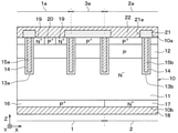
図1に示されるように、半導体装置は、IGBT素子を有するIGBT領域1と、FWD素子を有するFWD領域2とが共通の半導体基板10に形成されている。つまり、本実施形態の半導体装置は、RC(Reverse Conductingの略)-IGBTとされている。
As shown in FIG. 1, in the semiconductor device, the
具体的には、半導体装置は、N-型のドリフト層11を構成する半導体基板10を有している。なお、本実施形態では、半導体基板10は、シリコン基板で構成される。そして、ドリフト層11上には、P型のベース層12が形成されている。なお、ドリフト層11上とは、言い換えると半導体基板10の一面10a側のことである。
Specifically, the semiconductor device has a
半導体基板10には、ベース層12を貫通してドリフト層11に達するようにトレンチ13a、13bが形成されている。そして、各トレンチ13a、13bは、各トレンチ13a、13bの壁面を覆うように形成されたゲート絶縁膜14と、このゲート絶縁膜14の上に形成されたポリシリコン等により構成される第1、第2ゲート電極15a、15bとにより埋め込まれている。これにより、トレンチゲート構造が構成されている。
The
また、ドリフト層11を挟んでベース層12と反対側には、P+型のコレクタ層16およびN+型のカソード層17が形成されている。そして、本実施形態では、IGBT領域1とFWD領域2とは、半導体基板10の他面10b側に形成される層がコレクタ層16であるか、カソード層17であるかによって区画されている。すなわち、本実施形態では、コレクタ層16上の部分がIGBT領域1とされ、カソード層17上の部分がFWD領域2とされている。
Further, a P +
コレクタ層16およびカソード層17を挟んでドリフト層11と反対側(すなわち、半導体基板10の他面10b)には、コレクタ層16およびカソード層17と電気的に接続される下部電極18が形成されている。つまり、IGBT領域1においてはコレクタ電極として機能し、FWD領域2においてはカソード電極として機能する下部電極18が形成されている。本実施形態では、下部電極18が第2電極に相当している。
A
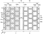
ここで、本実施形態におけるトレンチ13a、13bの形状(すなわち、トレンチゲート構造の形状)について、図1および図2を参照しつつ説明する。なお、以下では、半導体基板10の面方向における一方向をX軸方向とし、半導体基板10の面方向における一方向であって、X軸方向と直交する方向をY軸方向とし、X軸方向およびY軸方向と直交する方向をZ軸方向とする。図1中では、紙面左右方向がX軸方向となり、紙面垂直方向がY軸方向となり、紙面上下方向がZ軸方向となる。図2中では、紙面左右方向がX軸方向となり、紙面上下方向がY軸方向となり、紙面垂直方向がZ軸方向となる。本実施形態では、Y軸方向が第1方向に相当し、X軸方向が第2方向に相当している。また、後述する各図においても、適宜X軸方向、Y軸方向、Z軸方向を示している。そして、図2は、後述する層間絶縁膜21および上部電極22を省略して示し、断面図ではないが、理解をし易くするために第1、第2ゲート電極15a、15bにハッチングを施してある。また、後述する図2に対応する各図においても、層間絶縁膜21および上部電極22を省略し、第1、第2ゲート電極15a、15bにハッチングを施してある。
Here, the shapes of the
半導体基板10には、IGBT領域1にIGBT用トレンチ13aが形成され、FWD領域2にFWD用トレンチ13bが形成されており、各トレンチ13a、13bはZ軸方向を深さ方向として掘り下げられている。
In the
IGBT用トレンチ13aは、Y軸方向に沿って延設されたIGBT用第1トレンチ131aと、X軸方向に沿って延設されたIGBT用第2トレンチ132aとが連通されることで構成され、格子状とされている。なお、本実施形態では、IGBT用第1トレンチ131aは、X軸方向に沿って3本以上の複数本形成されており、隣合うIGBT用第1トレンチ131a同士の間隔が等しくされている。また、IGBT用第2トレンチ132aは、Y軸方向に沿って3本以上の複数本形成されており、隣合うIGBT用第2トレンチ132a同士の間隔が等しくされている。
The
FWD用トレンチ13bは、Y軸方向に沿って延設されたFWD用第1トレンチ131bと、X軸方向に沿って延設されたFWD用第2トレンチ132bとが連通されることで構成され、格子状とされている。
The
なお、本実施形態では、FWD用第1トレンチ131bは、X軸方向に沿って3本以上の複数本形成されている。そして、隣合うFWD用第1トレンチ131b同士の間隔は、互いに等しくされていると共に、隣合うIGBT用第1トレンチ131a同士の間隔とも等しくされている。また、FWD用第2トレンチ132bは、Y軸方向に沿って3本以上の複数本形成されている。そして、隣合うFWD用第2トレンチ132b同士の間隔は、互いに等しくされていると共に、隣合うIGBT用第2トレンチ132a同士の間隔とも等しくされている。
In this embodiment, a plurality of three or more
また、本実施形態では、1つのIGBT用第1トレンチ131aに対して反対側に突出する2つのIGBT用第2トレンチ132aは、Y軸方向に沿ってずれて配置されている。つまり、1つのIGBT用第1トレンチ131aに対して反対側に突出する2つのIGBT用第2トレンチ132aは、非対称とされている。同様に、1つのFWD用第1トレンチ131bに対して反対側に突出する2つのFWD用第2トレンチ132bは、Y軸方向に沿ってずれて配置されている。つまり、1つのFWD用第1トレンチ131bに対して反対側に突出する2つのFWD用第2トレンチ132bは、非対称とされている。
Further, in the present embodiment, the two IGBT
本実施形態では、このようにIGBT用トレンチ13aおよびFWD用トレンチ13bが形成されている。そして、IGBT用トレンチ13aとFWD用トレンチ13bとの間には、X軸方向に沿って延びるトレンチが形成されていない。つまり、本実施形態では、IGBT用トレンチ13aとFWD用トレンチ13bとは、連通されておらず、分離された状態となっている。このため、IGBT用トレンチ13aに埋め込まれた第1ゲート電極15aと、FWD用トレンチ13bに埋め込まれた第2ゲート電極15bとは、分離された状態となっており、電気的に絶縁された状態となっている。
In the present embodiment, the
そして、IGBT用トレンチ13aに埋め込まれた第1ゲート電極15aは、図示しないゲート配線を介して所定のゲート電圧が印加されるゲート駆動回路と接続される。一方、FWD用トレンチ13bに埋め込まれた第2ゲート電極15bは、例えば、後述する上部電極22と接続されて上部電極22の電位に維持される。
The
なお、IGBT用トレンチ13aおよびFWD用トレンチ13bについて、より詳しくは、第1ゲート電極15aが配置されたトレンチをIGBT用トレンチ13aとし、第2ゲート電極15bが配置されたトレンチをFWD用トレンチ13bとする。すなわち、本実施形態では、図1に示されるように、コレクタ層16とカソード層17との境界上にもトレンチが形成されているが、このトレンチには図2に示されるように第2ゲート電極15bが配置されている。このため、このトレンチは、FWD用トレンチ13bとなる。
Regarding the
以下では、IGBT用トレンチ13aのうちの最もFWD用トレンチ13b側のものをIGBT用端部トレンチ133aともいう。また、FWD用トレンチ13bのうちの最もIGBT用トレンチ13a側のものをFWD用端部トレンチ133bともいう。なお、本実施形態では、FWD用端部トレンチ133bは、X軸方向における中心がコレクタ層16とカソード層17との境界と略一致するように構成されている。
In the following, among the
また、以下では、IGBT用端部トレンチ133aの中心とFWD用端部トレンチ133bの中心との間の領域を分離セル領域3aともいう。また、IGBT領域1のうちの分離セル領域3と異なる領域をIGBTセル領域1aともいい、FWD領域2のうちの分離セル領域3と異なる領域をFWDセル領域2aともいう。
Further, in the following, the region between the center of the
なお、IGBT用端部トレンチ133aの中心とは、IGBT用端部トレンチ133aにおけるX軸方向の中心であり、FWD用端部トレンチ133bの中心とは、FWD用端部トレンチ133bにおけるX軸方向の中心のことである。そして、本実施形態では、FWD用端部トレンチ133bの中心がコレクタ層16とカソード層17との境界と略一致するように構成されている。このため、IGBT領域1に分離セル領域3aが含まれることになり、FWD領域2は全てFWDセル領域1bとなる。
The center of the
また、IGBT用端部トレンチ133aの中心とFWD用端部トレンチ133bの中心との間の距離を分離セルピッチW1とする。つまり、分離セル領域3aにおけるX軸方向に沿った距離を分離セルピッチW1とする。
Further, the distance between the center of the
また、X軸方向に沿って隣合うIGBT用第1トレンチ131a同士の中心間の距離をIGBT用第1トレンチピッチD1aとする。また、Y軸方向に沿って隣合うIGBT用第2トレンチ132a同士の中心間の距離をIGBT用第2トレンチピッチD2aとする。なお、IGBT用第1トレンチ131aの中心とは、IGBT用第1トレンチ131aにおけるX軸方向の中心のことであり、IGBT用第2トレンチ132aの中心とは、IGBT用第2トレンチ132aにおけるY軸方向の中心のことである。
Further, the distance between the centers of the adjacent
同様に、X軸方向に沿って隣合うFWD用第1トレンチ131b同士の中心間の距離をFWD用第1トレンチピッチD1bとする。また、Y軸方向に沿って隣合うFWD用第2トレンチ132bの中心間の距離をFWD用第2トレンチピッチD2bとする。なお、FWD用第1トレンチ131bの中心とは、FWD用第1トレンチ131bにおけるX軸方向の中心のことであり、FWD用第2トレンチ132bの中心とは、FWD用第2トレンチ132bにおけるY軸方向の中心のことである。
Similarly, the distance between the centers of the FWD
また、本実施形態では、上記のように、隣合うIGBT用第1トレンチ131a同士の間隔と、隣合うFWD用第1トレンチ131b同士の間隔とが等しくされている。このため、IGBT用第1トレンチピッチD1aとFWD用第1トレンチピッチD1bとは等しくなっている。また、隣合うIGBT用第2トレンチ132a同士の間隔と、隣合うFWD用第2トレンチ132b同士の間隔とが等しくされている。このため、IGBT用第2トレンチピッチD2aとFWD用第2トレンチピッチD2bとは等しくなっている。
Further, in the present embodiment, as described above, the distance between the adjacent
そして、本実施形態では、分離セルピッチW1は、各トレンチピッチD1a、D2a、D1b、D2bより狭くされている。このため、本実施形態の分離セル領域3aは、例えば、分離セルピッチW1がIGBT用第1トレンチピッチD1aおよびFWD用第1トレンチピッチD1b以上とされている場合と比較して、トレンチ密度が高くなっている。
In the present embodiment, the separation cell pitch W1 is narrower than the trench pitches D1a, D2a, D1b, and D2b, respectively. Therefore, in the
以上が本実施形態におけるトレンチ13a、13bの構成である。
The above is the configuration of the
そして、各IGBTセル領域1aにおいては、ベース層12の表層部に、ドリフト層11よりも高不純物濃度とされたN+型のエミッタ領域19、およびベース層12よりも高不純物濃度とされたP+型のコンタクト領域20がそれぞれ形成されている。具体的には、本実施形態では、エミッタ領域19は、IGBT用トレンチ13aに沿って形成されている。つまり、エミッタ領域19は、半導体基板10の面方向に対する法線方向から視たとき、枠状に形成されている。そして、コンタクト領域20は、エミッタ領域19と隣接しつつエミッタ領域19で囲まれるように形成され、IGBT用トレンチ13aと離れた位置に形成されている。なお、ベース層12の表層部とは、言い換えると、半導体基板10の一面10a側のことである。
Then, in each
また、FWDセル領域2aおよび分離セル領域3aでは、ベース層12の表層部に、IGBTセル領域1aに形成されるコンタクト領域20と同様のコンタクト領域20が形成されている。なお、本実施形態では、分離セル領域3aにはエミッタ領域19は形成されていない。つまり、IGBT用端部トレンチ133aの分離セル領域3側には、エミッタ領域19が形成されていない。すなわち、本実施形態では、分離セル領域3aをIGBT素子として動作しなくなるようにしている。これにより、IGBT動作時にFWD用端部トレンチ133bに配置された第2ゲート電極15bがゲート干渉し、FWD素子の特性が変動することを抑制できる。
Further, in the
半導体基板10の一面10a上には、BPSG(Borophosphosilicate Glassの略)等で構成される層間絶縁膜21が形成されている。そして、層間絶縁膜21上には、層間絶縁膜21に形成されたコンタクトホール21aを通じてエミッタ領域19およびコンタクト領域20(すなわち、ベース層12)と電気的に接続される第1電極としての上部電極22が形成されている。つまり、層間絶縁膜21上には、IGBT領域1においてエミッタ電極として機能し、FWD領域2においてアノード電極として機能する上部電極22が形成されている。
An interlayer insulating
なお、分離セル領域3aでは、図1とは別断面において、層間絶縁膜21にコンタクト領域20を露出させるコンタクトホール21aが形成されている。より詳しくは、本実施形態の半導体装置は、特に図示しないが、上記IGBT領域1およびFWD領域2を囲むように外周領域が配置されている。そして、分離セル領域3aでは、外周領域の近傍で層間絶縁膜21にコンタクトホールが形成され、当該コンタクトホール21aを通じてコンタクト領域20が上部電極22と電気的に接続されている。
In the
このため、後述するようにダイオード動作をする際、分離セル領域3aのコンタクトホール21aが外周領域の近傍に形成されているため、分離セル領域3aを介して上部電極22にキャリアが流れ難くなり、分離セル領域3aがダイオード動作し難くなる。これにより、ダイオード動作時にIGBT用端部トレンチ133aに配置された第1ゲート電極15aがゲート干渉し、IGBT素子の特性が変動することを抑制できる。
Therefore, when the diode operation is performed as described later, since the
そして、上記のように構成されていることにより、FWDセル領域2aにおいては、ベース層12およびコンタクト領域20をアノードとし、ドリフト層11、カソード層17をカソードとしてPN接合されたFWD素子が構成される。
With the above configuration, in the
以上が本実施形態における半導体装置の構成である。なお、本実施形態では、N型、N+型、N-型が第1導電型に相当しており、P型、P+型が第2導電型に相当している。また、本実施形態では、上記のように、半導体基板10は、コレクタ層16、カソード層17、ドリフト層11、ベース層12、エミッタ領域19、コンタクト領域20を有する構成とされている。
The above is the configuration of the semiconductor device in this embodiment. In this embodiment, N-type, N + type, and N - type correspond to the first conductive type, and P-type and P + type correspond to the second conductive type. Further, in the present embodiment, as described above, the
次に、上記半導体装置の作動について、簡単に説明する。 Next, the operation of the semiconductor device will be briefly described.
まず、半導体装置は、下部電極18に上部電極22より高い電圧が印加されると、ベース層12とドリフト層11との間に形成されるPN接合が逆導通状態となって空乏層が形成される。そして、第1ゲート電極15aに、絶縁ゲート構造の閾値電圧Vth未満であるローレベル(例えば、0V)の電圧が印加されているときには、上部電極22と下部電極18との間に電流は流れない。
First, in the semiconductor device, when a voltage higher than that of the
そして、IGBT素子をオン状態にするには、下部電極18に上部電極22より高い電圧が印加された状態で、第1ゲート電極15aに、絶縁ゲート構造の閾値電圧Vth以上であるハイレベルの電圧が印加されるようにする。これにより、ベース層12のうちの第1ゲート電極15aが配置されるIGBT用トレンチ13aと接している部分には、反転層が形成される。そして、エミッタ領域19から反転層を介して電子がドリフト層11に供給されることによってコレクタ層16から正孔がドリフト層11に供給され、伝導度変調によりドリフト層11の抵抗値が低下することでオン状態となる。
Then, in order to turn on the IGBT element, a high level voltage equal to or higher than the threshold voltage Vth of the insulated gate structure is applied to the
また、IGBT素子をオフ状態にし、FWD素子をオン状態にする(すなわち、FWD素子をダイオード動作させる)際には、上部電極22と下部電極18に印加する電圧をスイッチングし、上部電極22に下部電極18より高い電圧を印加する。そして、第1ゲート電極15aに絶縁ゲート構造の閾値電圧Vth未満であるローレベル(例えば、0V)の電圧を印加する。これにより、ベース層12のうちのIGBT用第1トレンチ131aと接する部分に反転層が形成されなくなり、ベース層12から正孔が供給されると共にカソード層17から電子が供給されることでFWD素子がダイオード動作をする。
Further, when the IGBT element is turned off and the FWD element is turned on (that is, the FWD element is operated by a diode), the voltage applied to the
その後、FWD素子をオン状態からオフ状態にする際には、下部電極18に上部電極22より高い電圧を印加する逆電圧印加を行う。つまり、FWD素子に順方向電流が流れている状態から当該電流を遮断する際、下部電極18に上部電極22より高い電圧を印加する逆電圧印加を行う。これにより、FWD素子がリカバリ状態となった後にオフ状態となる。
After that, when the FWD element is turned from the on state to the off state, a reverse voltage is applied to the
この際、半導体装置では、等電位線が各トレンチ13a、13bを避けるように湾曲して形成される。そして、本実施形態では、分離セルピッチW1を各トレンチピッチD1a、D2a、D1b、D2bより狭くしている。このため、分離セルピッチW1が各トレンチピッチD1a、D2a、D1b、D2b以上とされている場合と比較して、分離セル領域3aのトレンチ密度が高くなる。したがって、分離セル領域3aにおいても等電位線がベース層12側に入り込み難くなり、分離セル領域3aでも電界集中が発生することを抑制できる。したがって、分離セル領域3aにおける耐圧を高くできるため、半導体装置の耐圧を高くできる。
At this time, in the semiconductor device, the equipotential lines are formed so as to avoid the
以上説明したように、本実施形態では、分離セルピッチW1が各トレンチピッチD1a、D2a、D1b、D2bより狭くされている。このため、分離セル領域3aでは、分離セルピッチW1が各トレンチピッチD1a、D2a、D1b、D2b以上とされている場合と比較して、トレンチ密度が高くなる。これにより、分離セル領域3aにおいても等電位線がベース層12側に入り込み難くなり、分離セル領域3aでも電界集中が発生することを抑制できる。したがって、分離セル領域3aにおける耐圧を高くできるため、半導体装置の耐圧を高くできる。
As described above, in the present embodiment, the separation cell pitch W1 is narrower than the trench pitches D1a, D2a, D1b, and D2b. Therefore, in the
(第2実施形態)
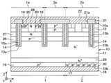
第2実施形態について説明する。本実施形態は、第1実施形態に対し、分離セル領域3aにダミートレンチを形成したものである。その他に関しては第1実施形態と同様であるため、ここでは説明を省略する。
(Second Embodiment)
The second embodiment will be described. In this embodiment, a dummy trench is formed in the
本実施形態では、図3および図4に示されるように、分離セル領域3aには、Y軸方向に沿って延び、IGBT用トレンチ13aおよびFWD用トレンチ13bとは分離された1つのダミートレンチ23が形成されている。本実施形態では、このダミートレンチ23は、IGBT用トレンチ13aおよびFWD用トレンチ13bよりも深く形成されている。
In the present embodiment, as shown in FIGS. 3 and 4, one
そして、ダミートレンチ23は、ダミートレンチ23の壁面を覆うように形成されたダミー絶縁膜24と、このダミー絶縁膜24の上に形成されたポリシリコン等により構成されるダミー電極25とにより埋め込まれている。なお、本実施形態のダミー電極25は、図1とは別断面において、上部電極22と電気的に接続されている。
The
ここで、本実施形態では、ダミートレンチ23の中心と、IGBT用端部トレンチ133aの中心との間の距離を分離用第1トレンチピッチL1とする。また、ダミートレンチ23の中心と、FWD用端部トレンチ133bの中心との間の距離を分離用第2トレンチピッチL2とする。なお、ダミートレンチ23の中心とは、ダミートレンチ23におけるX軸方向の中心のことである。また、分離セルピッチW1は、分離用第1トレンチピッチL1と分離用第2トレンチピッチL2との和となる。
Here, in the present embodiment, the distance between the center of the
そして、本実施形態では、分離用第1トレンチピッチL1および分離用第2トレンチピッチL2が各トレンチピッチD1a、D2a、D1b、D2bより狭くされ、かつ分離セルピッチW1が各トレンチピッチD1a、D2a、D1b、D2bより狭くされている。なお、本実施形態では、分離用第1トレンチピッチL1と分離用第2トレンチピッチL2とは等しくされている。 In the present embodiment, the separation first trench pitch L1 and the separation second trench pitch L2 are narrower than the respective trench pitches D1a, D2a, D1b, and D2b, and the separation cell pitch W1 is the respective trench pitches D1a, D2a, and D1b. , Narrower than D2b. In this embodiment, the separation first trench pitch L1 and the separation second trench pitch L2 are equal to each other.
以上説明したように、本実施形態では、分離セル領域3aにダミートレンチ23が形成されている。このため、分離セル領域3aでは、さらにトレンチ密度を高くでき、さらに耐圧の向上を図ることができる。
As described above, in the present embodiment, the
また、ダミートレンチ23は、IGBT用トレンチ13aおよびFWD用トレンチ13bよりも深くまで形成されている。このため、ダミートレンチ23がIGBT用トレンチ13aおよびFWD用トレンチ13bと同じ深さとされている場合と比較して、分離セル領域3aでは、さらに等電位線がベース層12側に入り込み難くなる。したがって、さらに分離セル領域3aの耐圧を向上できる。
Further, the
(第2実施形態の変形例)
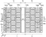
上記第2実施形態の変形例について説明する。上記第2実施形態において、図5に示されるように、分離セル領域3aには、複数のダミートレンチ23がX軸方向に沿って配列されるように形成されていてもよい。この場合、IGBT用端部トレンチ133aの中心と、IGBT用端部トレンチ133aと隣合うダミートレンチ23の中心との間の距離を分離用第1トレンチピッチL1とする。また、FWD用端部トレンチ133bの中心と、FWD用端部トレンチ133bと隣合うダミートレンチ23の中心との間の距離を分離用第2トレンチピッチL2とする。そして、隣合うダミートレンチ23同士の中心間の距離を分離用第3トレンチピッチL3とする。この場合、分離用第1~第3トレンチピッチL1~L3は、各トレンチピッチD1a、D2a、D1b、D2bより狭くなる。
(Modified example of the second embodiment)
A modified example of the second embodiment will be described. In the second embodiment, as shown in FIG. 5, a plurality of
また、このような変形例において、さらに複数のダミートレンチ23を形成するようにしてもよい。この場合は、隣合うダミートレンチ23同士の中心間の最大距離を分離用第3トレンチピッチL3とすればよい。
Further, in such a modification, a plurality of
さらに、上記第2実施形態において、図6に示されるように、ダミートレンチ23は、Y軸方向に沿って複数に分離されていてもよい。なお、このような構成とする場合には、Y軸方向に沿って隣合うダミートレンチ23の間隔を分離用第4トレンチピッチL4とすると、ダミートレンチ23は、分離用第4トレンチピッチL4も各トレンチピッチD1a、D2a、D1b、D2bより狭くなるように構成される。これにより、分離セル領域3aのトレンチ密度の向上を図ることができ、上記第2実施形態と同様の効果を得ることができる。
Further, in the second embodiment, as shown in FIG. 6, the
(第3実施形態)
第3実施形態について説明する。第3実施形態は、第2実施形態に対し、分離セルピッチW1と、各トレンチピッチD1a、D2a、D1b、D2bとの関係を変更したものである。その他に関しては第1実施形態と同様であるため、ここでは説明を省略する。
(Third Embodiment)
The third embodiment will be described. The third embodiment is a modification of the second embodiment in which the relationship between the separation cell pitch W1 and the trench pitches D1a, D2a, D1b, and D2b is changed. Others are the same as those in the first embodiment, and thus description thereof will be omitted here.
本実施形態では、図7に示されるように、分離セルピッチW1は、各トレンチピッチD1a、D2a、D1b、D2bよりも広くされている。しかしながら、分離用第1トレンチピッチL1および分離用第2トレンチピッチL2は、それぞれ各トレンチピッチD1a、D2a、D1b、D2bよりも狭くされている。 In this embodiment, as shown in FIG. 7, the separation cell pitch W1 is wider than the trench pitches D1a, D2a, D1b, and D2b, respectively. However, the separation first trench pitch L1 and the separation second trench pitch L2 are narrower than the respective trench pitches D1a, D2a, D1b, and D2b, respectively.
以上説明したように、分離セルピッチW1は、分離用第1、第2トレンチピッチL1、L2が各トレンチピッチD1a、D2a、D1b、D2bより狭くなるのであれば、各トレンチピッチD1a、D2a、D1b、D2bより広くされていてもよい。このような半導体装置としても、分離セル領域3aのトレンチ密度が向上するため、上記第2実施形態と同様の効果を得ることができる。
As described above, the separation cell pitch W1 has the separation cell pitches D1a, D2a, D1b, respectively, if the separation first and second trench pitches L1 and L2 are narrower than the respective trench pitches D1a, D2a, D1b and D2b. It may be wider than D2b. Even in such a semiconductor device, since the trench density of the
なお、特に図示しないが、本実施形態は、上記第2実施形態の変形例を適宜組み合わせることも可能である。この場合、例えば、図5の構成を採用する場合には、分離用第1~第3トレンチピッチL1~L3が各トレンチピッチD1a、D2a、D1b、D2bより狭くなるようにすればよい。 Although not shown in particular, the present embodiment can be appropriately combined with modified examples of the second embodiment. In this case, for example, when the configuration of FIG. 5 is adopted, the separation first to third trench pitches L1 to L3 may be narrower than the respective trench pitches D1a, D2a, D1b, and D2b.
(第4実施形態)
第4実施形態について説明する。第4実施形態は、第1実施形態に対し、分離セル領域3aのベース層12の構成を変更したものである。その他に関しては、第1実施形態と同様であるため、ここでは説明を省略する。
(Fourth Embodiment)
The fourth embodiment will be described. The fourth embodiment is a modification of the first embodiment in which the configuration of the
本実施形態では、図8に示されるように、分離セル領域3aでは、ベース層12の深さがIGBTセル領域1aおよびFWDセル領域2aよりも深く形成されている。つまり、分離セル領域3aは、IGBTセル領域1aおよびFWDセル領域1bよりもベース層12における単位体積当たりの不純物量が高くなるように構成されている。
In the present embodiment, as shown in FIG. 8, in the
なお、このような半導体装置におけるベース層12は、例えば、次のように製造される。すなわち、ベース層12は、半導体基板10にP型の不純物をイオン注入して熱処理することで形成される。この場合、分離セル領域3aを構成する部分では、イオン注入時の加速電圧を大きくする、または複数回に渡ってイオン注入を行うことにより、IGBTセル領域1aおよびFWDセル領域2aよりもベース層12が深くなるように形成される。
The
以上説明したように、本実施形態では、分離セル領域3aでは、IGBTセル領域1aおよびFWDセル領域2aよりもベース層12が深くまで形成されている。このため、分離セル領域3aでは、IGBTセル領域1aおよびFWDセル領域2aよりも、ベース層12とドリフト層11との間の空乏層が半導体基板10の他面10b側に延びた状態となる。したがって、分離セル領域3aでは、さらに等電位線がベース層12側に入り込み難くなり、分離セル領域3aで電界集中が発生することを抑制できる。
As described above, in the present embodiment, in the separated
(第4実施形態の変形例)
上記第4実施形態の変形例について説明する。上記第4実施形態において、分離セル領域3aにおけるベース層12は、IGBTセル領域1aおよびFWDセル領域2aにおけるベース層12よりも高不純物濃度とされていてもよい。これによれば、さらに等電位線がベース層12側に入り込み難くなり、分離セル領域3で電界集中が発生することを抑制できる。なお、このような構成では、分離セル領域3aにおけるベース層12は、IGBTセル領域1aおよびFWDセル領域1bにおけるベース層12と同じ深さとされていてもよい。
(Modified example of the fourth embodiment)
A modified example of the fourth embodiment will be described. In the fourth embodiment, the
また、上記第4実施形態では、分離セルピッチW1は、各トレンチピッチD1a、D2a、D1b、D2b以上とされていてもよい。このような半導体装置としても、分離セル領域3aのベース層12を変更することによって電界集中が発生することを抑制できるため、耐圧の向上を図ることができる。
Further, in the fourth embodiment, the separation cell pitch W1 may be set to the trench pitches D1a, D2a, D1b, D2b or more. Even in such a semiconductor device, it is possible to suppress the occurrence of electric field concentration by changing the
(第5実施形態)
第5実施形態について説明する。第5実施形態は、第1実施形態に対し、分離セル領域3aに連通トレンチを形成したものである。その他に関しては、第1実施形態と同様であるため、ここでは説明を省略する。
(Fifth Embodiment)
A fifth embodiment will be described. In the fifth embodiment, a communication trench is formed in the
本実施形態では、図9に示されるように、分離セル領域3aには、IGBT用端部トレンチ133aとFWD用端部トレンチ133bとを繋ぐ連通トレンチ134が形成されている。具体的には、連通トレンチ134は、X軸方向に沿って延びるように形成されていると共に、複数形成されている。そして、IGBT用端部トレンチ133aとFWD用端部トレンチ133bとは、各連通トレンチ134を介して連通されている。つまり、本実施形態では、IGBT用トレンチ13aとFWD用トレンチ13bとが一体的に形成されている。
In the present embodiment, as shown in FIG. 9, a
そして、連通トレンチ134には、第1ゲート電極15aと第2ゲート電極15bとを絶縁する絶縁膜135が配置されている。
An insulating
以上説明したように、本実施形態では、分離セル領域3aに連通トレンチ134が形成されている。このため、分離セル領域3aのトレンチ密度をさらに高くできる。したがって、さらに分離セル領域3aでの電界集中が発生することを抑制できる。
As described above, in the present embodiment, the
(第5実施形態の変形例)
上記第5実施形態の変形例について説明する。上記第5実施形態において、分離セルピッチW1は、各トレンチピッチD1a、D2a、D1b、D2b以上とされていてもよい。このような半導体装置としても、分離セル領域3aに連通トレンチ134を形成することにより、連通トレンチ134が形成されていない場合と比較して電界集中が発生することを抑制できるため、耐圧の向上を図ることができる。
(Variation example of the fifth embodiment)
A modified example of the fifth embodiment will be described. In the fifth embodiment, the separation cell pitch W1 may be set to the trench pitches D1a, D2a, D1b, D2b or more. Even in such a semiconductor device, by forming the
また、上記第5実施形態において、連通トレンチ134は1つのみ形成されていてもよい。このような半導体装置としても、連通トレンチ134が形成されていない場合と比較すれば、トレンチ密度を高くできる。
Further, in the fifth embodiment, only one
さらに、上記第5実施形態において、第1ゲート電極15aと第2ゲート電極15bとが絶縁されるのであれば、第1ゲート電極15aおよび第2ゲート電極15bは、一部が連通トレンチ134内まで延設されていてもよい。
Further, in the fifth embodiment, if the
(第6実施形態)
第6実施形態について説明する。第6実施形態は、第1実施形態に対し、ピラー領域、バリア領域、電界緩和領域を形成したものである。その他に関しては、第1実施形態と同様であるため、ここでは説明を省略する。
(Sixth Embodiment)
The sixth embodiment will be described. The sixth embodiment forms a pillar region, a barrier region, and an electric field relaxation region with respect to the first embodiment. Others are the same as those in the first embodiment, and thus description thereof will be omitted here.
本実施形態では、図10および図11に示されるように、IGBTセル領域1a、分離セル領域3a、FWDセル領域2bにおいて、ドリフト層11とベース層12との間に、ベース層12よりも低不純物濃度とされたP--型の電界緩和領域26が形成されている。そして、IGBTセル領域1a、FWDセル領域2a、分離セル領域3aにおいて、電界緩和領域26とベース層12との間には、ドリフト層11より高不純物濃度とされたN型のバリア領域27が形成されている。なお、各トレンチ13a、13bは、ベース層12、バリア領域27、電界緩和領域26を貫通してドリフト層11に達するように形成されている。
In this embodiment, as shown in FIGS. 10 and 11, the
また、本実施形態では、IGBTセル領域1aおよびFWDセル領域2aにおいて、エミッタ領域19が形成されている。具体的には、IGBTセル領域1aでは、エミッタ領域19は、当該IGBTセル領域1aの1セルを形造る一対のIGBT用第1トレンチ131aに対し、それぞれ略中央部に位置する部分に沿って形成されている。同様に、FWDセル領域2aでは、エミッタ領域19は、当該FWDセル領域2aの1セルを形造る一対のFWD用第1トレンチ131bに対し、それぞれ略中央部に位置する部分に沿って形成されている。
Further, in the present embodiment, the
また、IGBTセル領域1aおよびFWDセル領域2aには、ベース層12の表層部に、コンタクト領域20に囲まれるように、N型のピラー領域28が形成されている。ピラー領域28は、バリア領域27に達し、バリア領域27と接続されるように形成されている。ピラー領域28は、上部電極22に対してショットキー接続されている。
Further, in the
そして、本実施形態では、IGBTセル領域1aおよびFWDセル領域2aでは上記のようにエミッタ領域19、コンタクト領域20、ピラー領域28が形成されているため、半導体基板10の一面10aには、ベース層12も露出した状態となっている。
In the present embodiment, since the
また、ドリフト層11のうちのベース層12側と反対側(すなわち、半導体基板10の他面10b側)には、ドリフト層11よりも高不純物濃度とされたN型のフィールドストップ層(以下では、FS層という)29が形成されている。このFS層29は、空乏層の広がりを防ぐことで耐圧と定常損失の性能向上を図ると共に、半導体基板10の他面10b側から注入されるホールの注入量を制御するためのものである。
Further, on the side of the
さらに、本実施形態では、カソード層17には、部分的にp+型の注入領域30が形成された状態となっている。本実施形態では、注入領域30は、複数形成されて格子状に形成されているが、1つのみとされていてもよいし、Y軸方向に沿って延びるストライプ状とされていてもよいし、不規則に形成されていてもよい。なお、この注入領域30は、コンタクト領域20と同じ不純物濃度とされている。
Further, in the present embodiment, the
以上説明した本実施形態では、バリア領域27がピラー領域28を介して上部電極22の電位に維持される。このため、この半導体装置では、FWD素子をオンさせる際には、ベース層12とバリア領域27との間のpn接合によって構成されるダイオードがオンし難くなり、上部電極22の電位を上昇させることでオンする。したがって、ダイオード動作を安定させることができる。
In the present embodiment described above, the
また、本実施形態の半導体装置では、バリア領域27とドリフト層11との間には、P型の電界緩和領域26が形成されている。このため、電界緩和領域26が形成されていない場合と比較して、電界緩和領域26とドリフト層11との間に構成されるpn接合により、等電位線が各トレンチ13の間に入り込み難くなり、さらに耐圧の向上を図ることができる。
Further, in the semiconductor device of the present embodiment, a P-type electric
(他の実施形態)
本発明は上記した実施形態に限定されるものではなく、特許請求の範囲に記載した範囲内において適宜変更が可能である。
(Other embodiments)
The present invention is not limited to the above-described embodiment, and can be appropriately modified within the scope of the claims.
例えば、上記各実施形態では、第1導電型をN型とし、第2導電型をP型とした例について説明したが、第1導電型をP型とし、第2導電型をN型とすることもできる。 For example, in each of the above embodiments, an example in which the first conductive type is N-type and the second conductive type is P-type has been described, but the first conductive type is P-type and the second conductive type is N-type. You can also do it.
また、上記各実施形態において、分離セル領域3aでは、IGBT用トレンチ13aと接するようにエミッタ領域19が形成され、当該エミッタ領域19も上部電極22と接続されるようにしてもよい。
Further, in each of the above embodiments, in the
さらに、上記各実施形態において、分離セル領域3aでは、外周領域から離れた位置にコンタクトホール21aが形成されていてもよい。例えば、上記第1実施形態では、図1において、分離セル領域3aのコンタクト領域20を露出させるコンタクトホール21aが形成されていてもよい。
Further, in each of the above embodiments, in the
また、上記各実施形態において、コレクタ層16とカソード層17との境界は、他の位置に形成されていてもよい。例えば、コレクタ層16とカソード層17との境界は、IGBT用端部トレンチ133aの直下に形成されるようにしてもよいし、IGBT用端部トレンチ133aとFWD用端部トレンチ133bとの間の中央部に形成されるようにしてもよい。つまり、分離セル領域3aは、FWD領域2内にのみ含まれるようにしてもよいし、IGBT領域1およびFWD領域2に含まれるようにしてもよい。
Further, in each of the above embodiments, the boundary between the
さらに、上記第1、第2、第4~第6実施形態において、例えば、隣合うIGBT用第1トレンチ131a同士の間隔が異なっており、IGBT用第1トレンチピッチD1aが部分毎に異なっていてもよい。同様に、隣合うIGBT用第2トレンチ132a同士の間隔、隣合うFWD用第1トレンチ131b同士の間隔、隣合うFWD用第2トレンチ132b同士の間隔も異なっていてもよい。これらのような構成とする場合には、分離セルピッチW1は、各トレンチピッチD1a、D2a、D1b、D2bの最小距離より狭くされていればよい。
Further, in the first, second, fourth to sixth embodiments, for example, the intervals between the adjacent
また、上記第1~第5実施形態において、FWD領域2にもエミッタ領域19が形成されていてもよい。そして、上記第6実施形態において、FWD領域2にエミッタ領域19が形成されていなくてもよい。
Further, in the first to fifth embodiments, the
さらに、上記第2実施形態において、ダミー電極25は、上部電極22等と接続されておらず、浮遊状態とされていてもよい。
Further, in the second embodiment, the
また、上記各実施形態を適宜組み合わせてもよい。例えば、上記第4実施形態は、上記第2、第3実施形態にも適宜組み合わせ可能である。また、上記第5実施形態は、上記第2~第4実施形態にも適宜組み合わせ可能である。さらに、上記第6実施形態は、上記第2~第5実施形態にも適宜組み合わせ可能である。そして、各実施形態を組み合わせたもの同士をさらに組み合わせるようにしてもよい。 In addition, each of the above embodiments may be combined as appropriate. For example, the fourth embodiment can be appropriately combined with the second and third embodiments. Further, the fifth embodiment can be appropriately combined with the second to fourth embodiments. Further, the sixth embodiment can be appropriately combined with the second to fifth embodiments. Then, the combinations of the respective embodiments may be further combined.
1 IGBT領域
2 FWD領域
3a 分離セル領域
10 半導体基板
11 ドリフト層
12 ベース層
13a IGBT用トレンチ
13b FWD用トレンチ
14 ゲート絶縁膜
15a 第1ゲート電極
15b 第2ゲート電極
16 コレクタ層
17 カソード層
18 下部電極(第2電極)
22 上部電極(第1電極)
131a IGBT用第1トレンチ
131b FWD用第1トレンチ
132a IGBT用第2トレンチ
132b FWD用第2トレンチ
1
22 Upper electrode (first electrode)
131a First trench for
Claims (11)
第1導電型のドリフト層(11)と、
前記ドリフト層上に形成された第2導電型のベース層(12)と、
前記ベース層を貫通するトレンチ(13a、13b)の壁面に形成されたゲート絶縁膜(14)と、前記ゲート絶縁膜上に形成されたゲート電極(15a、15b)と、を有する複数のトレンチゲート構造と、
前記ベース層の表層部であって、前記IGBT領域に形成された前記トレンチと接するように形成された第1導電型のエミッタ領域(19)と、
前記ドリフト層を挟んで前記ベース層側と反対側に形成された第2導電型のコレクタ層(16)と、
前記ドリフト層を挟んで前記ベース層と反対側に形成されると共に前記コレクタ層と隣接する第1導電型のカソード層(17)と、
前記ベース層および前記エミッタ領域と電気的に接続される第1電極(22)と、
前記コレクタ層および前記カソード層と電気的に接続される第2電極(18)と、を備え、
前記コレクタ層上の領域が前記IGBT領域とされ、前記カソード層上の領域が前記FWD領域とされており、
前記トレンチは、前記IGBT領域に形成される前記ゲート電極としての第1ゲート電極(14a)が配置されるIGBT用トレンチ(13a)と、前記FWD領域に形成され、前記第1ゲート電極とは別に制御される前記ゲート電極としての第2ゲート電極(14b)が配置されるFWD用トレンチ(13b)であり、
前記IGBT用トレンチは、前記半導体基板の面方向における一方向に沿った第1方向に延設されたIGBT用第1トレンチ(131a)と、前記半導体基板の面方向における前記第1方向と交差する第2方向に延設されたIGBT用第2トレンチ(132a)とが連通された格子状とされており、
前記FWD用トレンチは、前記第1方向に延設されたFWD用第1トレンチ(131b)と、前記第2方向に延設されたFWD用第2トレンチ(132b)とが連通された格子状とされ、
前記IGBT用第1トレンチのうちの最も前記FWD用トレンチ側に位置するトレンチ(133a)の中心と、前記FWD用第1トレンチのうちの最も前記IGBT用トレンチ側に位置するトレンチ(133b)の中心との間を分離セル領域(3a)とすると共に前記分離セル領域における前記第2方向の距離を分離セルピッチ(W1)とし、隣合う前記IGBT用第1トレンチ同士の中心間の最小距離をIGBT用第1トレンチピッチ(D1a)とし、隣合う前記IGBT用第2トレンチ同士の中心間の最小距離をIGBT用第2トレンチピッチ(D2a)とし、隣合う前記FWD用第1トレンチ同士の中心間の最小距離をFWD用第1トレンチピッチ(D1b)とし、隣合う前記FWD用第2トレンチ同士の中心間の最小距離をFWD用第2トレンチピッチ(D2b)とすると、
前記分離セルピッチは、前記IGBT用第1トレンチピッチ、前記IGBT用第2トレンチピッチ、前記FWD用第1トレンチピッチ、前記FWD用第2トレンチピッチよりも狭くされている半導体装置。 A semiconductor device in which the IGBT region (1) and the FWD region (2) are formed on a common semiconductor substrate (10).
The first conductive type drift layer (11) and
The second conductive type base layer (12) formed on the drift layer and
A plurality of trench gates having a gate insulating film (14) formed on the wall surface of the trench (13a, 13b) penetrating the base layer and a gate electrode (15a, 15b) formed on the gate insulating film. Structure and
A first conductive type emitter region (19) which is a surface layer portion of the base layer and is formed so as to be in contact with the trench formed in the IGBT region.
A second conductive type collector layer (16) formed on the side opposite to the base layer side with the drift layer interposed therebetween.
A first conductive type cathode layer (17) formed on the side opposite to the base layer with the drift layer interposed therebetween and adjacent to the collector layer.
A first electrode (22) electrically connected to the base layer and the emitter region,
A second electrode (18) electrically connected to the collector layer and the cathode layer is provided.
The region on the collector layer is the IGBT region, and the region on the cathode layer is the FWD region.
The trench is formed in the FWD region and is separate from the IGBT trench (13a) in which the first gate electrode (14a) as the gate electrode is arranged, which is formed in the IGBT region. A FWD trench (13b) in which a second gate electrode (14b) as the controlled gate electrode is arranged.
The IGBT trench intersects the IGBT first trench (131a) extending in a first direction along one direction in the surface direction of the semiconductor substrate and the first direction in the surface direction of the semiconductor substrate. It has a grid pattern in which it communicates with the second trench (132a) for the IGBT extending in the second direction.
The FWD trench has a grid pattern in which the FWD first trench (131b) extending in the first direction and the FWD second trench (132b) extending in the second direction are communicated with each other. Being done
The center of the trench (133a) located closest to the FWD trench side of the first IGBT trench and the center of the trench (133b) located closest to the IGBT trench side of the FWD first trench. The distance between the two is the separation cell region (3a), the distance in the second direction in the separation cell region is the separation cell pitch (W1), and the minimum distance between the centers of the adjacent first trenches for the IGBT is for the IGBT. The first trench pitch (D1a) is set, and the minimum distance between the centers of the adjacent second trenches for IGBT is defined as the second trench pitch for IGBT (D2a), and the minimum distance between the centers of the adjacent first trenches for FWD is set. Assuming that the distance is the FWD first trench pitch (D1b) and the minimum distance between the centers of the adjacent FWD second trenches is the FWD second trench pitch (D2b).
The semiconductor device whose separation cell pitch is narrower than the first trench pitch for the IGBT, the second trench pitch for the IGBT, the first trench pitch for the FWD, and the second trench pitch for the FWD.
前記ダミートレンチ(23)には、ダミー絶縁膜(24)とダミー電極(25)とが配置されている請求項1に記載の半導体装置。 A dummy trench (23) extending along the first direction is formed in the separation cell region.
The semiconductor device according to claim 1, wherein a dummy insulating film (24) and a dummy electrode (25) are arranged in the dummy trench (23).
第1導電型のドリフト層(11)と、
前記ドリフト層上に形成された第2導電型のベース層(12)と、
前記ベース層を貫通するトレンチ(13a、13b)の壁面に形成されたゲート絶縁膜(14)と、前記ゲート絶縁膜上に形成されたゲート電極(15a、15b)と、を有する複数のトレンチゲート構造と、
前記ベース層の表層部であって、前記IGBT領域に形成された前記トレンチと接するように形成された第1導電型のエミッタ領域(19)と、
前記ドリフト層を挟んで前記ベース層側と反対側に形成された第2導電型のコレクタ層(16)と、
前記ドリフト層を挟んで前記ベース層と反対側に形成されると共に前記コレクタ層と隣接する第1導電型のカソード層(17)と、
前記ベース層および前記エミッタ領域と電気的に接続される第1電極(22)と、
前記コレクタ層および前記カソード層と電気的に接続される第2電極(18)と、を備え、
前記コレクタ層上の領域が前記IGBT領域とされ、前記カソード層上の領域が前記FWD領域とされており、
前記トレンチは、前記IGBT領域に形成される前記ゲート電極としての第1ゲート電極(14a)が配置されるIGBT用トレンチ(13a)と、前記FWD領域に形成され、前記第1ゲート電極とは別に制御される前記ゲート電極としての第2ゲート電極(14b)が配置されるFWD用トレンチ(13b)であり、
前記IGBT用トレンチは、前記半導体基板の面方向における一方向に沿った第1方向に延設されたIGBT用第1トレンチ(131a)と、前記半導体基板の面方向における前記第1方向と交差する第2方向に延設されたIGBT用第2トレンチ(132a)とが連通された格子状とされており、
前記FWD用トレンチは、前記第1方向に延設されたFWD用第1トレンチ(131b)と、前記第2方向に延設されたFWD用第2トレンチ(132b)とが連通された格子状とされ、
前記IGBT用第1トレンチのうちの最も前記FWD用トレンチ側に位置するトレンチ(133a)の中心と、前記FWD用第1トレンチのうちの最も前記IGBT用トレンチ側に位置するトレンチ(133b)の中心との間を分離セル領域(3a)とすると共に前記分離セル領域における前記第2方向の距離を分離セルピッチ(W1)とし、
前記分離セル領域には、前記第1方向に沿って延設された1つのダミートレンチ(23)が形成され、
前記ダミートレンチ(23)には、ダミー絶縁膜(24)とダミー電極(25)とが配置されており、
隣合う前記IGBT用第1トレンチ同士の中心間の最小距離をIGBT用第1トレンチピッチ(D1a)とし、隣合う前記IGBT用第2トレンチ同士の中心間の最小距離をIGBT用第2トレンチピッチ(D2a)とし、隣合う前記FWD用第1トレンチ同士の中心間の最小距離をFWD用第1トレンチピッチ(D1b)とし、隣合う前記FWD用第2トレンチ同士の中心間の最小距離をFWD用第2トレンチピッチ(D2b)とし、前記ダミートレンチの中心と、当該ダミートレンチと隣合う前記IGBT用第1トレンチの中心との間の距離を分離用第1トレンチピッチ(L1)とし、前記ダミートレンチの中心と、当該ダミートレンチと隣合う前記FWD用第1トレンチの中心との間の距離を分離用第2トレンチピッチ(L2)とすると、
前記分離セルピッチは、前記IGBT用第1トレンチピッチ、前記IGBT用第2トレンチピッチ、前記FWD用第1トレンチピッチ、前記FWD用第2トレンチピッチの少なくとも1つより大きくされ、
前記分離用第1トレンチピッチおよび前記分離用第2トレンチピッチは、前記IGBT用第1トレンチピッチ、前記IGBT用第2トレンチピッチ、前記FWD用第1トレンチピッチ、前記FWD用第2トレンチピッチよりも狭くされている半導体装置。 A semiconductor device in which the IGBT region (1) and the FWD region (2) are formed on a common semiconductor substrate (10).
The first conductive type drift layer (11) and
The second conductive type base layer (12) formed on the drift layer and
A plurality of trench gates having a gate insulating film (14) formed on the wall surface of the trench (13a, 13b) penetrating the base layer and a gate electrode (15a, 15b) formed on the gate insulating film. Structure and
A first conductive type emitter region (19) which is a surface layer portion of the base layer and is formed so as to be in contact with the trench formed in the IGBT region.
A second conductive type collector layer (16) formed on the side opposite to the base layer side with the drift layer interposed therebetween.
A first conductive type cathode layer (17) formed on the side opposite to the base layer with the drift layer interposed therebetween and adjacent to the collector layer.
A first electrode (22) electrically connected to the base layer and the emitter region,
A second electrode (18) electrically connected to the collector layer and the cathode layer is provided.
The region on the collector layer is the IGBT region, and the region on the cathode layer is the FWD region.
The trench is formed in the FWD region and is separate from the IGBT trench (13a) in which the first gate electrode (14a) as the gate electrode is arranged, which is formed in the IGBT region. A FWD trench (13b) in which a second gate electrode (14b) as the controlled gate electrode is arranged.
The IGBT trench intersects the IGBT first trench (131a) extending in a first direction along one direction in the surface direction of the semiconductor substrate and the first direction in the surface direction of the semiconductor substrate. It has a grid pattern in which it communicates with the second trench (132a) for the IGBT extending in the second direction.
The FWD trench has a grid pattern in which the FWD first trench (131b) extending in the first direction and the FWD second trench (132b) extending in the second direction are communicated with each other. Being done
The center of the trench (133a) located closest to the FWD trench side of the first IGBT trench and the center of the trench (133b) located closest to the IGBT trench side of the FWD first trench. The distance between the and the separated cell region (3a) is defined as the separation cell region (3a), and the distance in the second direction in the separation cell region is defined as the separation cell pitch (W1).
In the separation cell region, one dummy trench (23) extending along the first direction is formed.
A dummy insulating film (24) and a dummy electrode (25) are arranged in the dummy trench (23).
The minimum distance between the centers of the adjacent first trenches for IGBT is defined as the first trench pitch for IGBT (D1a), and the minimum distance between the centers of the adjacent second trenches for IGBT is defined as the second trench pitch for IGBT (D1a). D2a), the minimum distance between the centers of the adjacent FWD first trenches is the FWD first trench pitch (D1b), and the minimum distance between the centers of the adjacent FWD second trenches is the FWD first. The 2 trench pitch (D2b) is used, and the distance between the center of the dummy trench and the center of the first IGBT trench adjacent to the dummy trench is set as the separation first trench pitch (L1). Assuming that the distance between the center and the center of the FWD first trench adjacent to the dummy trench is the separation second trench pitch (L2),
The separation cell pitch is made larger than at least one of the first trench pitch for the IGBT, the second trench pitch for the IGBT, the first trench pitch for the FWD, and the second trench pitch for the FWD.
The separation first trench pitch and the separation second trench pitch are larger than the IGBT first trench pitch, the IGBT second trench pitch, the FWD first trench pitch, and the FWD second trench pitch. Semiconductor devices that are narrowed.
第1導電型のドリフト層(11)と、
前記ドリフト層上に形成された第2導電型のベース層(12)と、
前記ベース層を貫通するトレンチ(13a、13b)の壁面に形成されたゲート絶縁膜(14)と、前記ゲート絶縁膜上に形成されたゲート電極(15a、15b)と、を有する複数のトレンチゲート構造と、
前記ベース層の表層部であって、前記IGBT領域に形成された前記トレンチと接するように形成された第1導電型のエミッタ領域(19)と、
前記ドリフト層を挟んで前記ベース層側と反対側に形成された第2導電型のコレクタ層(16)と、
前記ドリフト層を挟んで前記ベース層と反対側に形成されると共に前記コレクタ層と隣接する第1導電型のカソード層(17)と、
前記ベース層および前記エミッタ領域と電気的に接続される第1電極(22)と、
前記コレクタ層および前記カソード層と電気的に接続される第2電極(18)と、を備え、
前記コレクタ層上の領域が前記IGBT領域とされ、前記カソード層上の領域が前記FWD領域とされており、
前記トレンチは、前記IGBT領域に形成される前記ゲート電極としての第1ゲート電極(14a)が配置されるIGBT用トレンチ(13a)と、前記FWD領域に形成され、前記第1ゲート電極とは別に制御される前記ゲート電極としての第2ゲート電極(14b)が配置されるFWD用トレンチ(13b)であり、
前記IGBT用トレンチは、前記半導体基板の面方向における一方向に沿った第1方向に延設されたIGBT用第1トレンチ(131a)と、前記半導体基板の面方向における前記第1方向と交差する第2方向に延設されたIGBT用第2トレンチ(132a)とが連通された格子状とされており、
前記FWD用トレンチは、前記第1方向に延設されたFWD用第1トレンチ(131b)と、前記第2方向に延設されたFWD用第2トレンチ(132b)とが連通された格子状とされ、
前記IGBT用第1トレンチのうちの最も前記FWD用トレンチ側に位置するトレンチ(133a)の中心と、前記FWD用第1トレンチのうちの最も前記IGBT用トレンチ側に位置するトレンチ(133b)の中心との間を分離セル領域(3a)とすると共に前記分離セル領域における前記第2方向の距離を分離セルピッチ(W1)とし、
前記分離セル領域には、前記第1方向に沿って延設された複数のダミートレンチ(23)が形成され、
前記ダミートレンチ(23)には、ダミー絶縁膜(24)とダミー電極(25)とが配置されており、
隣合う前記IGBT用第1トレンチ同士の中心間の最小距離をIGBT用第1トレンチピッチ(D1a)とし、隣合う前記IGBT用第2トレンチ同士の中心間の最小距離をIGBT用第2トレンチピッチ(D2a)とし、隣合う前記FWD用第1トレンチ同士の中心間の最小距離をFWD用第1トレンチピッチ(D1b)とし、隣合う前記FWD用第2トレンチ同士の中心間の最小距離をFWD用第2トレンチピッチ(D2b)とし、前記ダミートレンチの中心と、当該ダミートレンチと隣合う前記IGBT用第1トレンチの中心との間の距離を分離用第1トレンチピッチ(L1)とし、前記ダミートレンチの中心と、当該ダミートレンチと隣合う前記FWD用第1トレンチの中心との間の距離を分離用第2トレンチピッチ(L2)とし、隣合う前記ダミートレンチ同士の中心間の最大距離を分離用第3トレンチピッチ(L3)とすると、
前記分離セルピッチは、前記IGBT用第1トレンチピッチ、前記IGBT用第2トレンチピッチ、前記FWD用第1トレンチピッチ、前記FWD用第2トレンチピッチの少なくとも1つより大きくされ、
前記分離用第1トレンチピッチ、前記分離用第2トレンチピッチおよび前記分離用第3トレンチピッチは、前記IGBT用第1トレンチピッチ、前記IGBT用第2トレンチピッチ、前記FWD用第1トレンチピッチ、前記FWD用第2トレンチピッチよりも狭くされている半導体装置。 A semiconductor device in which the IGBT region (1) and the FWD region (2) are formed on a common semiconductor substrate (10).
The first conductive type drift layer (11) and
The second conductive type base layer (12) formed on the drift layer and
A plurality of trench gates having a gate insulating film (14) formed on the wall surface of the trench (13a, 13b) penetrating the base layer and a gate electrode (15a, 15b) formed on the gate insulating film. Structure and
A first conductive type emitter region (19) which is a surface layer portion of the base layer and is formed so as to be in contact with the trench formed in the IGBT region.
A second conductive type collector layer (16) formed on the side opposite to the base layer side with the drift layer interposed therebetween.
A first conductive type cathode layer (17) formed on the side opposite to the base layer with the drift layer interposed therebetween and adjacent to the collector layer.
A first electrode (22) electrically connected to the base layer and the emitter region,
A second electrode (18) electrically connected to the collector layer and the cathode layer is provided.
The region on the collector layer is the IGBT region, and the region on the cathode layer is the FWD region.
The trench is formed in the FWD region and is separate from the IGBT trench (13a) in which the first gate electrode (14a) as the gate electrode is arranged, which is formed in the IGBT region. A FWD trench (13b) in which a second gate electrode (14b) as the controlled gate electrode is arranged.
The IGBT trench intersects the IGBT first trench (131a) extending in a first direction along one direction in the surface direction of the semiconductor substrate and the first direction in the surface direction of the semiconductor substrate. It has a grid pattern in which it communicates with the second trench (132a) for the IGBT extending in the second direction.
The FWD trench has a grid pattern in which the FWD first trench (131b) extending in the first direction and the FWD second trench (132b) extending in the second direction are communicated with each other. Being done
The center of the trench (133a) located closest to the FWD trench side of the first IGBT trench and the center of the trench (133b) located closest to the IGBT trench side of the FWD first trench. The distance between the and the separated cell region (3a) is defined as the separation cell region (3a), and the distance in the second direction in the separation cell region is defined as the separation cell pitch (W1).
A plurality of dummy trenches (23) extending along the first direction are formed in the separation cell region.
A dummy insulating film (24) and a dummy electrode (25) are arranged in the dummy trench (23).
The minimum distance between the centers of the adjacent first trenches for IGBT is defined as the first trench pitch for IGBT (D1a), and the minimum distance between the centers of the adjacent second trenches for IGBT is defined as the second trench pitch for IGBT (D1a). D2a), the minimum distance between the centers of the adjacent FWD first trenches is the FWD first trench pitch (D1b), and the minimum distance between the centers of the adjacent FWD second trenches is the FWD first. The 2 trench pitch (D2b) is used, and the distance between the center of the dummy trench and the center of the first IGBT trench adjacent to the dummy trench is set as the separation first trench pitch (L1). The distance between the center and the center of the FWD first trench adjacent to the dummy trench is defined as the separation second trench pitch (L2), and the maximum distance between the centers of the adjacent dummy trenches is defined as the separation second. With 3 trench pitch (L3),
The separation cell pitch is made larger than at least one of the first trench pitch for the IGBT, the second trench pitch for the IGBT, the first trench pitch for the FWD, and the second trench pitch for the FWD.
The separation first trench pitch, the separation second trench pitch, and the separation third trench pitch are the IGBT first trench pitch, the IGBT second trench pitch, the FWD first trench pitch, and the above. A semiconductor device that is narrower than the second trench pitch for FWD.
前記分離セル領域のベース層は、前記IGBTセル領域および前記FWDセル領域のベース層よりも単位体積当たりの不純物量が高くされている請求項1ないし4のいずれか1つに記載の半導体装置。 It is assumed that the region of the IGBT region different from the separation cell region is referred to as the IGBT cell region (1a), and the region of the FWD region different from the separation cell region is referred to as the FWD cell region (2a).
The semiconductor device according to any one of claims 1 to 4, wherein the base layer of the separation cell region has a higher amount of impurities per unit volume than the base layer of the IGBT cell region and the FWD cell region.
前記連通トレンチには、前記第1ゲート電極と前記第2ゲート電極とを絶縁する絶縁膜(135)が配置されている請求項1ないし5のいずれか1つに記載の半導体装置。 In the separation cell region, the trench located closest to the FWD trench side of the first IGBT trench and the trench located closest to the IGBT trench side of the first FWD trench communicate with each other. A communication trench (134) is formed to allow the communication to be formed.
The semiconductor device according to any one of claims 1 to 5 , wherein an insulating film (135) that insulates the first gate electrode and the second gate electrode is arranged in the communication trench.
第1導電型のドリフト層(11)と、
前記ドリフト層上に形成された第2導電型のベース層(12)と、
前記ベース層を貫通するトレンチ(13a、13b)の壁面に形成されたゲート絶縁膜(14)と、前記ゲート絶縁膜上に形成されたゲート電極(15a、15b)と、を有する複数のトレンチゲート構造と、
前記ベース層の表層部であって、前記IGBT領域に形成された前記トレンチと接するように形成された第1導電型のエミッタ領域(19)と、
前記ドリフト層を挟んで前記ベース層側と反対側に形成された第2導電型のコレクタ層(16)と、
前記ドリフト層を挟んで前記ベース層と反対側に形成されると共に前記コレクタ層と隣接する第1導電型のカソード層(17)と、
前記ベース層および前記エミッタ領域と電気的に接続される第1電極(22)と、
前記コレクタ層および前記カソード層と電気的に接続される第2電極(18)と、を備え、
前記コレクタ層上の領域が前記IGBT領域とされ、前記カソード層上の領域が前記FWD領域とされており、
前記トレンチは、前記IGBT領域に形成される前記ゲート電極としての第1ゲート電極(14a)が配置されるIGBT用トレンチ(13a)と、前記FWD領域に形成され、前記第1ゲート電極とは別に制御される前記ゲート電極としての第2ゲート電極(14b)が配置されるFWD用トレンチ(13b)であり、
前記IGBT用トレンチは、前記半導体基板の面方向における一方向に沿った第1方向に延設されたIGBT用第1トレンチ(131a)と、前記半導体基板の面方向における前記第1方向と交差する第2方向に延設されたIGBT用第2トレンチ(132a)とが連通された格子状とされており、
前記FWD用トレンチは、前記第1方向に延設されたFWD用第1トレンチ(131b)と、前記第2方向に延設されたFWD用第2トレンチ(132b)とが連通された格子状とされ、
前記IGBT用第1トレンチのうちの最も前記FWD用トレンチ側に位置するトレンチ(133a)の中心と、前記FWD用第1トレンチのうちの最も前記IGBT用トレンチ側に位置するトレンチ(133b)の中心との間を分離セル領域(3a)とし、前記IGBT領域のうちの前記分離セル領域と異なる領域をIGBTセル領域(1a)とし、前記FWD領域のうちの前記分離セル領域と異なる領域をFWDセル領域(2a)とすると、
前記分離セル領域のベース層は、前記IGBTセル領域および前記FWDセル領域のベース層よりも単位体積当たりの不純物量が高くされており、
前記分離セル領域には、前記IGBT用第1トレンチのうちの最も前記FWD用トレンチ側に位置するトレンチと、前記FWD用第1トレンチのうちの最も前記IGBT用トレンチ側に位置するトレンチとを連通させる連通トレンチ(134)が形成されており、
前記連通トレンチには、前記第1ゲート電極と前記第2ゲート電極とを絶縁する絶縁膜(135)が配置されている半導体装置。 A semiconductor device in which the IGBT region (1) and the FWD region (2) are formed on a common semiconductor substrate (10).
The first conductive type drift layer (11) and
The second conductive type base layer (12) formed on the drift layer and
A plurality of trench gates having a gate insulating film (14) formed on the wall surface of the trench (13a, 13b) penetrating the base layer and a gate electrode (15a, 15b) formed on the gate insulating film. Structure and
A first conductive type emitter region (19) which is a surface layer portion of the base layer and is formed so as to be in contact with the trench formed in the IGBT region.
A second conductive type collector layer (16) formed on the side opposite to the base layer side with the drift layer interposed therebetween.
A first conductive type cathode layer (17) formed on the side opposite to the base layer with the drift layer interposed therebetween and adjacent to the collector layer.
A first electrode (22) electrically connected to the base layer and the emitter region,
A second electrode (18) electrically connected to the collector layer and the cathode layer is provided.
The region on the collector layer is the IGBT region, and the region on the cathode layer is the FWD region.
The trench is formed in the FWD region and is separate from the IGBT trench (13a) in which the first gate electrode (14a) as the gate electrode is arranged, which is formed in the IGBT region. A FWD trench (13b) in which a second gate electrode (14b) as the controlled gate electrode is arranged.
The IGBT trench intersects the IGBT first trench (131a) extending in a first direction along one direction in the surface direction of the semiconductor substrate and the first direction in the surface direction of the semiconductor substrate. It has a grid pattern in which it communicates with the second trench (132a) for the IGBT extending in the second direction.
The FWD trench has a grid pattern in which the FWD first trench (131b) extending in the first direction and the FWD second trench (132b) extending in the second direction are communicated with each other. Being done
The center of the trench (133a) located closest to the FWD trench side of the first IGBT trench and the center of the trench (133b) located closest to the IGBT trench side of the first FWD trench. The area between the two is referred to as the separation cell region (3a), the region of the IGBT region different from the separation cell region is referred to as the IGBT cell region (1a), and the region of the FWD region different from the separation cell region is the FWD cell. Assuming the area (2a),
The base layer of the separation cell region has a higher amount of impurities per unit volume than the base layer of the IGBT cell region and the FWD cell region.
In the separation cell region, the trench located closest to the FWD trench side of the first IGBT trench and the trench located closest to the IGBT trench side of the first FWD trench communicate with each other. A communication trench (134) is formed to allow the communication to be formed.
A semiconductor device in which an insulating film (135) that insulates the first gate electrode and the second gate electrode is arranged in the communication trench .
第1導電型のドリフト層(11)と、
前記ドリフト層上に形成された第2導電型のベース層(12)と、
前記ベース層を貫通するトレンチ(13a、13b)の壁面に形成されたゲート絶縁膜(14)と、前記ゲート絶縁膜上に形成されたゲート電極(15a、15b)と、を有する複数のトレンチゲート構造と、
前記ベース層の表層部であって、前記IGBT領域に形成された前記トレンチと接するように形成された第1導電型のエミッタ領域(19)と、
前記ドリフト層を挟んで前記ベース層側と反対側に形成された第2導電型のコレクタ層(16)と、
前記ドリフト層を挟んで前記ベース層と反対側に形成されると共に前記コレクタ層と隣接する第1導電型のカソード層(17)と、
前記ベース層および前記エミッタ領域と電気的に接続される第1電極(22)と、
前記コレクタ層および前記カソード層と電気的に接続される第2電極(18)と、を備え、
前記コレクタ層上の領域が前記IGBT領域とされ、前記カソード層上の領域が前記FWD領域とされており、
前記トレンチは、前記IGBT領域に形成される前記ゲート電極としての第1ゲート電極(14a)が配置されるIGBT用トレンチ(13a)と、前記FWD領域に形成され、前記第1ゲート電極とは別に制御される前記ゲート電極としての第2ゲート電極(14b)が配置されるFWD用トレンチ(13b)であり、
前記IGBT用トレンチは、前記半導体基板の面方向における一方向に沿った第1方向に延設されたIGBT用第1トレンチ(131a)と、前記半導体基板の面方向における前記第1方向と交差する第2方向に延設されたIGBT用第2トレンチ(132a)とが連通された格子状とされており、
前記FWD用トレンチは、前記第1方向に延設されたFWD用第1トレンチ(131b)と、前記第2方向に延設されたFWD用第2トレンチ(132b)とが連通された格子状とされ、
前記IGBT用第1トレンチのうちの最も前記FWD用トレンチ側に位置するトレンチ(133a)の中心と、前記FWD用第1トレンチのうちの最も前記IGBT用トレンチ側に位置するトレンチ(133b)の中心との間を分離セル領域(3a)とすると、
前記分離セル領域には、前記IGBT用第1トレンチのうちの最も前記FWD用トレンチ側に位置するトレンチと、前記FWD用第1トレンチのうちの最も前記IGBT用トレンチ側に位置するトレンチとを連通させる連通トレンチ(134)が形成されており、
前記連通トレンチには、前記第1ゲート電極と前記第2ゲート電極とを絶縁する絶縁膜(135)が配置されている半導体装置。 A semiconductor device in which the IGBT region (1) and the FWD region (2) are formed on a common semiconductor substrate (10).
The first conductive type drift layer (11) and
The second conductive type base layer (12) formed on the drift layer and
A plurality of trench gates having a gate insulating film (14) formed on the wall surface of the trench (13a, 13b) penetrating the base layer and a gate electrode (15a, 15b) formed on the gate insulating film. Structure and
A first conductive type emitter region (19) which is a surface layer portion of the base layer and is formed so as to be in contact with the trench formed in the IGBT region.
A second conductive type collector layer (16) formed on the side opposite to the base layer side with the drift layer interposed therebetween.
A first conductive type cathode layer (17) formed on the side opposite to the base layer with the drift layer interposed therebetween and adjacent to the collector layer.
A first electrode (22) electrically connected to the base layer and the emitter region,
A second electrode (18) electrically connected to the collector layer and the cathode layer is provided.
The region on the collector layer is the IGBT region, and the region on the cathode layer is the FWD region.
The trench is formed in the FWD region and is separate from the IGBT trench (13a) in which the first gate electrode (14a) as the gate electrode is arranged, which is formed in the IGBT region. A FWD trench (13b) in which a second gate electrode (14b) as the controlled gate electrode is arranged.
The IGBT trench intersects the IGBT first trench (131a) extending in a first direction along one direction in the surface direction of the semiconductor substrate and the first direction in the surface direction of the semiconductor substrate. It has a grid pattern in which it communicates with the second trench (132a) for the IGBT extending in the second direction.
The FWD trench has a grid pattern in which the FWD first trench (131b) extending in the first direction and the FWD second trench (132b) extending in the second direction are communicated with each other. Being done
The center of the trench (133a) located closest to the FWD trench side of the first IGBT trench and the center of the trench (133b) located closest to the IGBT trench side of the FWD first trench. Assuming that the space between the and is the separation cell area (3a),
In the separation cell region, the trench located closest to the FWD trench side of the first IGBT trench and the trench located closest to the IGBT trench side of the first FWD trench communicate with each other. A communication trench (134) is formed to allow the communication to be formed.
A semiconductor device in which an insulating film (135) that insulates the first gate electrode and the second gate electrode is arranged in the communication trench.
前記電界緩和領域と前記ベース層との間には、第1導電型のバリア領域(27)が形成され、
前記ベース層の表層部には、前記第1電極と接続されると共に前記バリア領域と接続される第1導電型のピラー領域(28)が形成されている請求項1ないし10のいずれか1つに記載の半導体装置。 A second conductive type electric field relaxation region (26) is formed between the drift layer and the base layer.
A first conductive type barrier region (27) is formed between the electric field relaxation region and the base layer.
One of claims 1 to 10, wherein a first conductive type pillar region (28) connected to the first electrode and connected to the barrier region is formed on the surface layer portion of the base layer. The semiconductor device described in.
Priority Applications (4)
| Application Number | Priority Date | Filing Date | Title |
|---|---|---|---|
| JP2018169878A JP6996461B2 (en) | 2018-09-11 | 2018-09-11 | Semiconductor device |
| PCT/JP2019/033935 WO2020054447A1 (en) | 2018-09-11 | 2019-08-29 | Semiconductor device |
| CN201980058845.7A CN112673466B (en) | 2018-09-11 | 2019-08-29 | Semiconductor device |
| US17/197,308 US11476355B2 (en) | 2018-09-11 | 2021-03-10 | Semiconductor device |
Applications Claiming Priority (1)
| Application Number | Priority Date | Filing Date | Title |
|---|---|---|---|
| JP2018169878A JP6996461B2 (en) | 2018-09-11 | 2018-09-11 | Semiconductor device |
Publications (3)
| Publication Number | Publication Date |
|---|---|
| JP2020043237A JP2020043237A (en) | 2020-03-19 |
| JP2020043237A5 JP2020043237A5 (en) | 2021-03-25 |
| JP6996461B2 true JP6996461B2 (en) | 2022-01-17 |
Family
ID=69778271
Family Applications (1)
| Application Number | Title | Priority Date | Filing Date |
|---|---|---|---|
| JP2018169878A Active JP6996461B2 (en) | 2018-09-11 | 2018-09-11 | Semiconductor device |
Country Status (4)
| Country | Link |
|---|---|
| US (1) | US11476355B2 (en) |
| JP (1) | JP6996461B2 (en) |
| CN (1) | CN112673466B (en) |
| WO (1) | WO2020054447A1 (en) |
Families Citing this family (10)
| Publication number | Priority date | Publication date | Assignee | Title |
|---|---|---|---|---|
| JP7319601B2 (en) * | 2019-11-01 | 2023-08-02 | 株式会社東芝 | semiconductor equipment |
| JP7459666B2 (en) * | 2020-06-04 | 2024-04-02 | 三菱電機株式会社 | semiconductor equipment |
| WO2021254615A1 (en) * | 2020-06-18 | 2021-12-23 | Dynex Semiconductor Limited | Reverse conducting igbt with controlled anode injection |
| JP7456902B2 (en) | 2020-09-17 | 2024-03-27 | 株式会社東芝 | semiconductor equipment |
| JP7528743B2 (en) * | 2020-11-27 | 2024-08-06 | 三菱電機株式会社 | Semiconductor Device |
| JP7486407B2 (en) * | 2020-11-27 | 2024-05-17 | 三菱電機株式会社 | Semiconductor device and method for manufacturing the same |
| EP4139965A1 (en) * | 2021-03-31 | 2023-03-01 | Dynex Semiconductor Limited | Power semiconductor device |
| JP7852462B2 (en) * | 2022-11-04 | 2026-04-28 | 株式会社デンソー | Semiconductor equipment |
| CN121040233A (en) * | 2023-11-29 | 2025-11-28 | 富士电机株式会社 | Semiconductor devices |
| EP4583165A1 (en) * | 2024-01-04 | 2025-07-09 | Nio Technology (Anhui) Co., Ltd | Reverse conducting insulated-gate bipolar transistor and method of manufacturing |
Citations (4)
| Publication number | Priority date | Publication date | Assignee | Title |
|---|---|---|---|---|
| JP2009021557A (en) | 2007-06-14 | 2009-01-29 | Denso Corp | Semiconductor device |
| JP2012151470A (en) | 2011-01-17 | 2012-08-09 | Infineon Technologies Austria Ag | Semiconductor device and reverse conducting igbt |
| JP2016197678A (en) | 2015-04-06 | 2016-11-24 | 三菱電機株式会社 | Semiconductor device |
| JP2016225560A (en) | 2015-06-03 | 2016-12-28 | トヨタ自動車株式会社 | Semiconductor device |
Family Cites Families (26)
| Publication number | Priority date | Publication date | Assignee | Title |
|---|---|---|---|---|
| JP4799829B2 (en) | 2003-08-27 | 2011-10-26 | 三菱電機株式会社 | Insulated gate transistor and inverter circuit |
| JP4830360B2 (en) * | 2005-06-17 | 2011-12-07 | 株式会社デンソー | Semiconductor device and manufacturing method thereof |
| JP5470826B2 (en) * | 2008-12-08 | 2014-04-16 | 株式会社デンソー | Semiconductor device |
| JP2010263149A (en) * | 2009-05-11 | 2010-11-18 | Toyota Motor Corp | Semiconductor device |
| JP5768395B2 (en) * | 2010-07-27 | 2015-08-26 | 株式会社デンソー | Semiconductor device and control method thereof |
| US8716746B2 (en) | 2010-08-17 | 2014-05-06 | Denso Corporation | Semiconductor device |
| JP5321669B2 (en) * | 2010-11-25 | 2013-10-23 | 株式会社デンソー | Semiconductor device |
| JP5874210B2 (en) | 2011-06-23 | 2016-03-02 | トヨタ自動車株式会社 | diode |
| EP2725623B1 (en) * | 2011-09-08 | 2019-10-30 | Fuji Electric Co., Ltd. | Semiconductor device |
| US9159786B2 (en) * | 2012-02-20 | 2015-10-13 | Taiwan Semiconductor Manufacturing Company, Ltd. | Dual gate lateral MOSFET |
| JP5825201B2 (en) * | 2012-03-05 | 2015-12-02 | 株式会社デンソー | Semiconductor device and manufacturing method thereof |
| US9136158B2 (en) * | 2012-03-09 | 2015-09-15 | Taiwan Semiconductor Manufacturing Company, Ltd. | Lateral MOSFET with dielectric isolation trench |
| JP5942737B2 (en) * | 2012-09-24 | 2016-06-29 | 株式会社デンソー | Semiconductor device |
| JP6135636B2 (en) | 2014-10-17 | 2017-05-31 | トヨタ自動車株式会社 | Semiconductor device |
| JP6260515B2 (en) | 2014-11-13 | 2018-01-17 | 三菱電機株式会社 | Semiconductor device |
| WO2016080269A1 (en) * | 2014-11-17 | 2016-05-26 | 富士電機株式会社 | Semiconductor device and method for producing semiconductor device |
| JP6261494B2 (en) * | 2014-12-03 | 2018-01-17 | 三菱電機株式会社 | Power semiconductor device |
| JPWO2016113865A1 (en) * | 2015-01-14 | 2017-07-13 | 三菱電機株式会社 | Semiconductor device and manufacturing method thereof |
| WO2016114131A1 (en) * | 2015-01-16 | 2016-07-21 | 株式会社デンソー | Semiconductor device |
| JP6641983B2 (en) * | 2015-01-16 | 2020-02-05 | 株式会社デンソー | Semiconductor device |
| JP6334465B2 (en) * | 2015-06-17 | 2018-05-30 | 富士電機株式会社 | Semiconductor device |
| JP6428503B2 (en) * | 2015-06-24 | 2018-11-28 | 株式会社デンソー | Semiconductor device |
| US10559663B2 (en) * | 2016-10-14 | 2020-02-11 | Fuji Electric Co., Ltd. | Semiconductor device with improved current flow distribution |
| JP6589817B2 (en) * | 2016-10-26 | 2019-10-16 | 株式会社デンソー | Semiconductor device |
| WO2018220879A1 (en) * | 2017-05-31 | 2018-12-06 | 富士電機株式会社 | Semiconductor device |
| WO2019111572A1 (en) * | 2017-12-06 | 2019-06-13 | 富士電機株式会社 | Semiconductor device |
-
2018
- 2018-09-11 JP JP2018169878A patent/JP6996461B2/en active Active
-
2019
- 2019-08-29 CN CN201980058845.7A patent/CN112673466B/en active Active
- 2019-08-29 WO PCT/JP2019/033935 patent/WO2020054447A1/en not_active Ceased
-
2021
- 2021-03-10 US US17/197,308 patent/US11476355B2/en active Active
Patent Citations (4)
| Publication number | Priority date | Publication date | Assignee | Title |
|---|---|---|---|---|
| JP2009021557A (en) | 2007-06-14 | 2009-01-29 | Denso Corp | Semiconductor device |
| JP2012151470A (en) | 2011-01-17 | 2012-08-09 | Infineon Technologies Austria Ag | Semiconductor device and reverse conducting igbt |
| JP2016197678A (en) | 2015-04-06 | 2016-11-24 | 三菱電機株式会社 | Semiconductor device |
| JP2016225560A (en) | 2015-06-03 | 2016-12-28 | トヨタ自動車株式会社 | Semiconductor device |
Also Published As
| Publication number | Publication date |
|---|---|
| CN112673466B (en) | 2024-02-23 |
| WO2020054447A1 (en) | 2020-03-19 |
| US11476355B2 (en) | 2022-10-18 |
| CN112673466A (en) | 2021-04-16 |
| JP2020043237A (en) | 2020-03-19 |
| US20210202725A1 (en) | 2021-07-01 |
Similar Documents
| Publication | Publication Date | Title |
|---|---|---|
| JP6996461B2 (en) | Semiconductor device | |
| JP6589817B2 (en) | Semiconductor device | |
| JP6443267B2 (en) | Semiconductor device | |
| JP5636808B2 (en) | Semiconductor device | |
| JP6641983B2 (en) | Semiconductor device | |
| JP2007134625A (en) | Semiconductor device and manufacturing method thereof | |
| JP2016029710A (en) | Semiconductor device | |
| JP7435214B2 (en) | semiconductor equipment | |
| JP7172920B2 (en) | semiconductor equipment | |
| WO2017199679A1 (en) | Semiconductor device | |
| JP2016092163A (en) | Semiconductor device | |
| WO2016114131A1 (en) | Semiconductor device | |
| JP2021145026A (en) | Semiconductor device | |
| JP5664029B2 (en) | Semiconductor device | |
| JP2018182240A (en) | Semiconductor switching device and method of manufacturing the same | |
| JP5151175B2 (en) | Semiconductor device | |
| US20220310830A1 (en) | Semiconductor device | |
| WO2019098122A1 (en) | Semiconductor device | |
| JP2016096307A (en) | Semiconductor device | |
| JP7338242B2 (en) | semiconductor equipment | |
| JP7294004B2 (en) | semiconductor equipment | |
| JP4830732B2 (en) | Semiconductor device | |
| JP7596930B2 (en) | Semiconductor Device | |
| JP2025069398A (en) | Semiconductor Device |
Legal Events
| Date | Code | Title | Description |
|---|---|---|---|
| A711 | Notification of change in applicant |
Free format text: JAPANESE INTERMEDIATE CODE: A711 Effective date: 20201030 |
|
| A521 | Request for written amendment filed |
Free format text: JAPANESE INTERMEDIATE CODE: A821 Effective date: 20201030 |
|
| A621 | Written request for application examination |
Free format text: JAPANESE INTERMEDIATE CODE: A621 Effective date: 20201120 |
|
| A521 | Request for written amendment filed |
Free format text: JAPANESE INTERMEDIATE CODE: A523 Effective date: 20210212 |
|
| TRDD | Decision of grant or rejection written | ||
| A01 | Written decision to grant a patent or to grant a registration (utility model) |
Free format text: JAPANESE INTERMEDIATE CODE: A01 Effective date: 20211116 |
|
| A61 | First payment of annual fees (during grant procedure) |
Free format text: JAPANESE INTERMEDIATE CODE: A61 Effective date: 20211129 |
|
| R151 | Written notification of patent or utility model registration |
Ref document number: 6996461 Country of ref document: JP Free format text: JAPANESE INTERMEDIATE CODE: R151 |
|
| R250 | Receipt of annual fees |
Free format text: JAPANESE INTERMEDIATE CODE: R250 |
|
| R250 | Receipt of annual fees |
Free format text: JAPANESE INTERMEDIATE CODE: R250 |