JP6981760B2 - Semiconductor device - Google Patents
Semiconductor device Download PDFInfo
- Publication number
- JP6981760B2 JP6981760B2 JP2017045913A JP2017045913A JP6981760B2 JP 6981760 B2 JP6981760 B2 JP 6981760B2 JP 2017045913 A JP2017045913 A JP 2017045913A JP 2017045913 A JP2017045913 A JP 2017045913A JP 6981760 B2 JP6981760 B2 JP 6981760B2
- Authority
- JP
- Japan
- Prior art keywords
- wiring
- transistor
- terminal
- circuit
- image data
- Prior art date
- Legal status (The legal status is an assumption and is not a legal conclusion. Google has not performed a legal analysis and makes no representation as to the accuracy of the status listed.)
- Active
Links
Images


Description
本発明の一態様は、半導体装置に関する。 One aspect of the present invention relates to a semiconductor device.
なお本発明の一態様は、上記の技術分野に限定されない。本明細書等で開示する発明の技術分野は、物、方法、または、製造方法に関するものである。または、本発明の一態様は、プロセス、マシン、マニュファクチャ、または、組成物(コンポジション・オブ・マター)に関するものである。そのため、より具体的に本明細書で開示する本発明の一態様の技術分野としては、半導体装置、表示装置、液晶表示装置、発光装置、蓄電装置、撮像装置、記憶装置、プロセッサ、電子機器、それらの駆動方法、それらの製造方法、それらの検査方法、またはそれらのシステムを一例として挙げることができる。 It should be noted that one aspect of the present invention is not limited to the above technical fields. The technical field of the invention disclosed in the present specification and the like relates to a product, a method, or a manufacturing method. Alternatively, one aspect of the invention relates to a process, machine, manufacture, or composition (composition of matter). Therefore, more specifically, the technical fields of one aspect of the present invention disclosed in the present specification include semiconductor devices, display devices, liquid crystal display devices, light emitting devices, power storage devices, image pickup devices, storage devices, processors, electronic devices, and the like. Examples include their driving methods, their manufacturing methods, their inspection methods, or their systems.
テレビジョン(TV)は、大画面化に伴い、高精細度の映像を視聴できることが望まれている。日本国では、2015年に通信衛星(CS)およびケーブルテレビ等による4K実用放送が開始され、2016年に放送衛星(BS)による4K・8K試験放送が開始されている。今後、8K実用放送の開始が予定されている。そのため、8K放送に対応するための各種の電子機器が開発されている(非特許文献1)。8Kの実用放送では、4K放送、2K放送(フルハイビジョン放送)も併用される予定である。 As televisions (TVs) have larger screens, it is desired to be able to view high-definition images. In Japan, 4K practical broadcasting by communication satellites (CS) and cable TV started in 2015, and 4K / 8K test broadcasting by broadcasting satellites (BS) started in 2016. 8K practical broadcasting is scheduled to start in the future. Therefore, various electronic devices for supporting 8K broadcasting have been developed (Non-Patent Document 1). In 8K practical broadcasting, 4K broadcasting and 2K broadcasting (full high-definition broadcasting) will also be used together.
また、テレビジョンに限らず様々な電子機器に対して人工ニューラルネットワーク等を利用した人工知能を付する開発が進められている。人工ニューラルネットワークを利用することで、従来のノイマン型コンピュータよりも高性能なコンピュータが実現できると期待されており、近年、電子回路上で人工ニューラルネットワークを構築する種々の研究が進められている。非特許文献2には、人工ニューラルネットワークによる自己学習機能を備えたチップに関する技術が記載されている。
In addition, development is underway to add artificial intelligence using artificial neural networks and the like to various electronic devices, not limited to television. It is expected that a computer with higher performance than the conventional von Neumann computer can be realized by using an artificial neural network, and in recent years, various studies for constructing an artificial neural network on an electronic circuit have been promoted. Non-Patent
さらに、特許文献1には、チャネル形成領域に酸化物半導体を有するトランジスタを用いた記憶装置によって、人工ニューラルネットワークを用いた計算に必要な重みデータを保持する発明が開示されている。
Further,
8K放送の映像の解像度(水平・垂直の画素数)は7680×4320であり、4K(3840×2160)の4倍、2K(1920×1080)の16倍である。したがって、8K放送の映像を見る者は、2K放送の映像、または4K放送の映像等を見る者より高い臨場感を感じることができると期待される。 The resolution (horizontal / vertical pixel count) of the 8K broadcast image is 7680 × 4320, which is 4 times that of 4K (3840 × 2160) and 16 times that of 2K (1920 × 1080). Therefore, it is expected that a person who sees an 8K broadcast image can feel a higher sense of presence than a person who sees a 2K broadcast image, a 4K broadcast image, or the like.
本発明の一態様は、高解像度の画像に対応する画像データを生成する機能を有する半導体装置、およびその動作方法を提供することを課題の1つとする。または、本発明の一態様は、階調数の多い画像に対応する画像データを生成する機能を有する半導体装置、およびその動作方法を提供することを課題の1つとする。または、本発明の一態様は、様々な種類の放送に対応する半導体装置、およびその動作方法を提供することを課題の1つとする。または、本発明の一態様は、新規な半導体装置、およびその動作方法を提供することを課題の1つとする。 One aspect of the present invention is to provide a semiconductor device having a function of generating image data corresponding to a high-resolution image, and an operation method thereof. Alternatively, one aspect of the present invention is to provide a semiconductor device having a function of generating image data corresponding to an image having a large number of gradations, and an operation method thereof. Alternatively, one aspect of the present invention is to provide a semiconductor device corresponding to various types of broadcasting and an operation method thereof. Alternatively, one aspect of the present invention is to provide a novel semiconductor device and a method of operating the same.
なお本発明の一態様の課題は、上記列挙した課題に限定されない。上記列挙した課題は、他の課題の存在を妨げるものではない。なお他の課題は、以下の記載で述べる、本項目で言及していない課題である。本項目で言及していない課題は、当業者であれば明細書または図面等の記載から導き出せるものであり、これらの記載から適宜抽出することができる。なお、本発明の一態様は、上記列挙した記載、および他の課題のうち、少なくとも一つの課題を解決するものである。なお、本発明の一態様は、上記列挙した記載、および他の課題の全てを解決する必要はない。 The problems of one aspect of the present invention are not limited to the problems listed above. The issues listed above do not preclude the existence of other issues. Other issues are issues not mentioned in this item, which are described below. Issues not mentioned in this item can be derived from the description of the description, drawings, etc. by those skilled in the art, and can be appropriately extracted from these descriptions. In addition, one aspect of the present invention solves at least one of the above-listed descriptions and other problems. It should be noted that one aspect of the present invention does not need to solve all of the above-listed descriptions and other problems.
本発明の一態様は、表示部と、第1の回路と、を有し、表示部は、マトリクス状に配置された画素を有し、第1の回路は、ニューラルネットワークを有し、第1の回路は、第1の画像データから、対応する画像の解像度を第1の画像データより高めた第2の画像データを生成する機能を有することを特徴とする半導体装置である。 One aspect of the present invention includes a display unit and a first circuit, the display unit has pixels arranged in a matrix, and the first circuit has a neural network. The circuit is a semiconductor device characterized by having a function of generating a second image data from the first image data, in which the resolution of the corresponding image is higher than that of the first image data.
また、本発明の一態様は、表示部と、第1の回路と、エンコーダと、デコーダと、を有し、表示部は、マトリクス状に配置された画素を有し、第1の回路、エンコーダ、及びデコーダは、それぞれニューラルネットワークを有し、第1の回路は、第1の画像データから、対応する画像の解像度を第1の画像データより高めた第2の画像データを生成する機能を有し、エンコーダは、第2の画像データに対して特徴抽出をした第3の画像データを生成する機能を有し、デコーダは、第3の画像データを、第2の画像データのビット数を増加させることにより、階調数を第2の画像データより増加させた第4の画像データを生成する機能を有する半導体装置である。 Further, one aspect of the present invention includes a display unit, a first circuit, an encoder, and a decoder, and the display unit has pixels arranged in a matrix, and the first circuit, the encoder. , And the decoder each have a neural network, and the first circuit has a function of generating a second image data from the first image data in which the resolution of the corresponding image is higher than that of the first image data. However, the encoder has a function of generating a third image data obtained by extracting features from the second image data, and the decoder increases the number of bits of the third image data and the second image data. This is a semiconductor device having a function of generating a fourth image data in which the number of gradations is increased from that of the second image data.
また、上記態様において、第2の画像データにおける、階調を表現するための一の画素あたりのビット数は、第4の画像データにおける、階調を表現するための一の画素あたりのビット数の1/2より多くてもよい。 Further, in the above aspect, the number of bits per pixel for expressing gradation in the second image data is the number of bits per pixel for expressing gradation in the fourth image data. It may be more than 1/2 of.
また、上記態様において、第2の回路を有し、第2の回路は、ニューラルネットワークを有し、第2の回路は、第2の画像データに対して画像処理を行う機能を有してもよい。 Further, in the above aspect, even if the second circuit has a second circuit, the second circuit has a neural network, and the second circuit has a function of performing image processing on the second image data. good.
また、上記態様において、画素は、トランジスタを有し、トランジスタは、チャネル形成領域に金属酸化物を有してもよい。 Further, in the above embodiment, the pixel may have a transistor, and the transistor may have a metal oxide in the channel forming region.
また、上記態様において、画素は、トランジスタを有し、トランジスタは、チャネル形成領域に水素化アモルファスシリコンを有してもよい。 Further, in the above embodiment, the pixel may have a transistor, and the transistor may have hydrogenated amorphous silicon in the channel forming region.
本発明の一態様により、高解像度の画像に対応する画像データを生成する機能を有する半導体装置、およびその動作方法を提供することができる。または、本発明の一態様により、階調数の多い画像に対応する画像データを生成する機能を有する半導体装置、およびその動作方法を提供することができる。または、本発明の一態様により、様々な種類の放送に対応する半導体装置、およびその動作方法を提供することができる。または、本発明の一態様は、新規な半導体装置、およびその動作方法を提供することができる。 According to one aspect of the present invention, it is possible to provide a semiconductor device having a function of generating image data corresponding to a high-resolution image, and an operation method thereof. Alternatively, according to one aspect of the present invention, it is possible to provide a semiconductor device having a function of generating image data corresponding to an image having a large number of gradations, and an operation method thereof. Alternatively, according to one aspect of the present invention, it is possible to provide a semiconductor device corresponding to various types of broadcasting and an operation method thereof. Alternatively, one aspect of the present invention can provide a novel semiconductor device and a method of operating the same.
なお本発明の一態様の効果は、上記列挙した効果に限定されない。上記列挙した効果は、他の効果の存在を妨げるものではない。なお他の効果は、以下の記載で述べる、本項目で言及していない効果である。本項目で言及していない効果は、当業者であれば明細書または図面等の記載から導き出せるものであり、これらの記載から適宜抽出することができる。なお、本発明の一態様は、上記列挙した効果、および他の効果のうち、少なくとも一つの効果を有するものである。従って本発明の一態様は、場合によっては、上記列挙した効果を有さない場合もある。 The effect of one aspect of the present invention is not limited to the effects listed above. The effects listed above do not preclude the existence of other effects. The other effects are the effects not mentioned in this item, which are described below. Effects not mentioned in this item can be derived from the description in the specification, drawings, etc. by those skilled in the art, and can be appropriately extracted from these descriptions. In addition, one aspect of the present invention has at least one of the above-listed effects and other effects. Therefore, one aspect of the present invention may not have the effects listed above in some cases.
本明細書等において、人工ニューラルネットワーク(ANN、以後、ニューラルネットワークと呼称する。)とは、生物の神経回路網を模したモデル全般を指す。一般的には、ニューラルネットワークは、ニューロンを模したユニットが、シナプスを模したユニットを介して、互いに結合された構成となっている。 In the present specification and the like, an artificial neural network (ANN, hereinafter referred to as a neural network) refers to a general model that imitates a neural network of an organism. In general, a neural network has a structure in which units that imitate neurons are connected to each other via units that imitate synapses.
シナプスの結合(ニューロン同士の結合)の強度(重み係数ともいう。)は、ニューラルネットワークに既存の情報を与えることによって、変化させることができる。このように、ニューラルネットワークに既存の情報を与えて、結合強度を決める処理を「学習」と呼ぶ場合がある。 The strength (also referred to as the weighting factor) of synaptic connections (connections between neurons) can be changed by giving existing information to the neural network. In this way, the process of giving existing information to the neural network and determining the bond strength may be called "learning".
また、「学習」を行った(結合強度を定めた)ニューラルネットワークに対して、何らかの情報を与えることにより、その結合強度に基づいて新たな情報を出力することができる。このように、ニューラルネットワークにおいて、与えられた情報と結合強度に基づいて新たな情報を出力する処理を「推論」または「認知」と呼ぶ場合がある。 Further, by giving some information to the neural network that has been "learned" (the bond strength is determined), new information can be output based on the bond strength. In this way, in a neural network, the process of outputting new information based on given information and bond strength may be called "inference" or "cognition".
ニューラルネットワークのモデルとしては、例えば、ホップフィールド型、階層型等が挙げられる。特に、多層構造としたニューラルネットワークを「ディープニューラルネットワーク」(DNN)と呼称し、ディープニューラルネットワークによる機械学習を「ディープラーニング」と呼称する。なお、DNNには、全結合ニューラルネットワーク(FC−NN:Full Connected − Neural Network)、畳み込みニューラルネットワーク(CNN:Convolutional Neural Network)、再帰ニューラルネットワーク(RNN:Recurrent Neural Network)等が含まれる。 Examples of the neural network model include a Hopfield type and a hierarchical type. In particular, a neural network having a multi-layer structure is called a "deep neural network" (DNN), and machine learning by a deep neural network is called "deep learning". The DNN includes a fully connected neural network (FC-NN: Full Connected-Neural Network), a convolutional neural network (CNN: Convolutional Neural Network), a recurrent neural network (RNN), and the like.
本明細書等において、金属酸化物(metal oxide)とは、広い表現での金属の酸化物である。金属酸化物は、酸化物絶縁体、酸化物導電体(透明酸化物導電体を含む)、酸化物半導体(Oxide Semiconductorまたは単にOSともいう)等に分類される。例えば、トランジスタの活性層に金属酸化物を用いた場合、当該金属酸化物を酸化物半導体と呼称する場合がある。つまり、金属酸化物が増幅作用、整流作用、およびスイッチング作用の少なくとも1つを有するトランジスタのチャネル形成領域を構成し得る場合、当該金属酸化物を、金属酸化物半導体(metal oxide semiconductor)、略してOSと呼ぶことができる。また、OS FET(またはOSトランジスタ)と記載する場合においては、金属酸化物または酸化物半導体を有するトランジスタと換言することができる。 In the present specification and the like, a metal oxide is a metal oxide in a broad expression. Metal oxides are classified into oxide insulators, oxide conductors (including transparent oxide conductors), oxide semiconductors (also referred to as Oxide Semiconductor or simply OS) and the like. For example, when a metal oxide is used for the active layer of a transistor, the metal oxide may be referred to as an oxide semiconductor. That is, when a metal oxide can form a channel forming region of a transistor having at least one of an amplification action, a rectifying action, and a switching action, the metal oxide is referred to as a metal oxide semiconductor, abbreviated as a metal oxide semiconductor. It can be called an OS. Further, in the case of describing as an OS FET (or an OS transistor), it can be paraphrased as a transistor having a metal oxide or an oxide semiconductor.
半導体の不純物とは、例えば、半導体層を構成する主成分以外をいう。例えば、濃度が0.1原子%未満の元素は不純物である。不純物が含まれることにより、例えば、半導体にDOS(Density of States)が形成されることや、キャリア移動度が低下することや、結晶性が低下すること等が起こる場合がある。半導体が酸化物半導体である場合、半導体の特性を変化させる不純物としては、例えば、第1族元素、第2族元素、第13族元素、第14族元素、第15族元素、主成分以外の遷移金属等があり、特に、例えば、水素(水にも含まれる)、リチウム、ナトリウム、シリコン、ホウ素、リン、炭素、窒素等がある。酸化物半導体の場合、例えば水素等の不純物の混入によって酸素欠損を形成する場合がある。また、半導体がシリコン層である場合、半導体の特性を変化させる不純物としては、例えば、酸素、水素を除く第1族元素、第2族元素、第13族元素、第15族元素等がある。
The semiconductor impurities are, for example, other than the main components constituting the semiconductor layer. For example, an element having a concentration of less than 0.1 atomic% is an impurity. The inclusion of impurities may cause, for example, the formation of DOS (Density of States) in the semiconductor, the decrease in carrier mobility, the decrease in crystallinity, and the like. When the semiconductor is an oxide semiconductor, the impurities that change the characteristics of the semiconductor include, for example,
本明細書等において、「第1」、「第2」、「第3」という序数詞は、構成要素の混同を避けるために付したものである。従って、構成要素の数を限定するものではない。また、構成要素の順序を限定するものではない。また例えば、本明細書等の実施の形態の一において「第1」に言及された構成要素が、他の実施の形態、あるいは特許請求の範囲において「第2」に言及された構成要素とすることもありうる。また例えば、本明細書等の実施の形態の一において「第1」に言及された構成要素を、他の実施の形態、あるいは特許請求の範囲において省略することもありうる。 In the present specification and the like, the ordinal numbers "first", "second", and "third" are added to avoid confusion of the components. Therefore, the number of components is not limited. Moreover, the order of the components is not limited. Further, for example, the component referred to in "first" in one of the embodiments of the present specification and the like is regarded as another embodiment or the component referred to in "second" in the scope of claims. It is possible. Further, for example, the component referred to in "first" in one of the embodiments of the present specification and the like may be omitted in other embodiments or in the scope of claims.
実施の形態について図面を参照しながら説明している。但し、実施の形態は多くの異なる態様で実施することが可能であり、趣旨およびその範囲から逸脱することなく、その形態および詳細を様々に変更し得ることは当業者であれば容易に理解される。従って、本発明は、実施の形態の記載内容に限定して解釈されるものではない。なお、実施の形態の発明の構成において、同一部分または同様な機能を有する部分には同一の符号を異なる図面間で共通して用い、その繰り返しの説明は省略する。 The embodiment is described with reference to the drawings. However, it is easily understood by those skilled in the art that embodiments can be implemented in many different embodiments and that the embodiments and details can be varied in various ways without departing from the spirit and scope thereof. To. Therefore, the present invention is not construed as being limited to the description of the embodiments. In the configuration of the invention of the embodiment, the same reference numerals are commonly used between different drawings for the same parts or parts having similar functions, and the repeated description thereof will be omitted.
また、本明細書等において、「上に」、「下に」等の配置を示す語句は、構成同士の位置関係を、図面を参照して説明するために、便宜上用いている。構成同士の位置関係は、各構成を描写する方向に応じて適宜変化する。そのため、配置を示す語句は、明細書で説明した記載に限定されず、状況に応じて適切に言い換えることができる。 Further, in the present specification and the like, words and phrases indicating arrangements such as "above" and "below" are used for convenience in order to explain the positional relationship between the configurations with reference to the drawings. The positional relationship between the configurations changes appropriately depending on the direction in which each configuration is depicted. Therefore, the phrase indicating the arrangement is not limited to the description described in the specification, and can be appropriately paraphrased according to the situation.
また、「上」や「下」の用語は、構成要素の位置関係が直上または直下で、かつ、直接接していることを限定するものではない。例えば、「絶縁層A上の電極B」の表現であれば、絶縁層Aの上に電極Bが直接接して形成されている必要はなく、絶縁層Aと電極Bとの間に他の構成要素を含むものを除外しない。 Further, the terms "upper" and "lower" do not limit the positional relationship of the components to be directly above or directly below and to be in direct contact with each other. For example, in the case of the expression "electrode B on the insulating layer A", it is not necessary that the electrode B is formed in direct contact with the insulating layer A, and another configuration is formed between the insulating layer A and the electrode B. Do not exclude those that contain elements.
また、図面において、大きさ、層の厚さ、または領域は、説明の便宜上任意の大きさに示したものである。よって、必ずしもそのスケールに限定されない。なお図面は明確性を期すために模式的に示したものであり、図面に示す形状または値等に限定されない。例えば、ノイズによる信号、電圧、若しくは電流のばらつき、または、タイミングのずれによる信号、電圧、若しくは電流のばらつき等を含むことが可能である。 Further, in the drawings, the size, the thickness of the layer, or the area are shown in any size for convenience of explanation. Therefore, it is not necessarily limited to that scale. It should be noted that the drawings are schematically shown for the sake of clarity, and are not limited to the shapes or values shown in the drawings. For example, it is possible to include variations in the signal, voltage, or current due to noise, or variations in the signal, voltage, or current due to timing deviation.
また、図面において、斜視図等において、図面の明確性を期すために、一部の構成要素の記載を省略している場合がある。 Further, in the drawings, in the perspective view and the like, the description of some components may be omitted in order to ensure the clarity of the drawings.
また、図面において、同一の要素または同様な機能を有する要素、同一の材質の要素、あるいは同時に形成される要素等には同一の符号を付す場合があり、その繰り返しの説明は省略する場合がある。 Further, in the drawings, the same elements or elements having the same function, elements of the same material, elements formed at the same time, etc. may be designated by the same reference numerals, and the repeated description thereof may be omitted. ..
本明細書等において、トランジスタの接続関係を説明する際、ソースとドレインとの一方を、「ソースまたはドレインの一方」(または第1電極、または第1の端子)と表記し、ソースとドレインとの他方を「ソースまたはドレインの他方」(または第2電極、または第2の端子)と表記している。これは、トランジスタのソースとドレインは、トランジスタの構造または動作条件等によって変わるためである。なおトランジスタのソースとドレインの呼称については、ソース(ドレイン)端子や、ソース(ドレイン)電極等、状況に応じて適切に言い換えることができる。また、本明細書等では、ゲート以外の2つの端子を第1の端子、第2の端子と呼ぶ場合や、第3端子、第4端子と呼ぶ場合がある。また、本明細書等に記載するトランジスタが2つ以上のゲートを有するとき(この構成をデュアルゲート構造という場合がある)、それらのゲートを第1ゲート、第2ゲートと呼ぶ場合や、フロントゲート、バックゲートと呼ぶ場合がある。特に、「フロントゲート」という語句は、単に「ゲート」という語句に互いに言い換えることができる。また、「バックゲート」という語句は、単に「ゲート」という語句に互いに言い換えることができる。なお、ボトムゲートとは、トランジスタの作製時において、チャネル形成領域よりも先に形成される端子のことをいい、「トップゲート」とは、トランジスタの作製時において、チャネル形成領域よりも後に形成される端子のことをいう。 In the present specification and the like, when explaining the connection relationship of transistors, one of the source and the drain is referred to as "one of the source or the drain" (or the first electrode or the first terminal), and the source and the drain are referred to as each other. The other of the above is referred to as "the other of the source or drain" (or the second electrode, or the second terminal). This is because the source and drain of the transistor change depending on the structure of the transistor, operating conditions, and the like. The names of the source and drain of the transistor can be appropriately paraphrased according to the situation, such as the source (drain) terminal and the source (drain) electrode. Further, in the present specification and the like, two terminals other than the gate may be referred to as a first terminal and a second terminal, or may be referred to as a third terminal and a fourth terminal. Further, when the transistor described in the present specification or the like has two or more gates (this configuration may be referred to as a dual gate structure), those gates may be referred to as a first gate and a second gate, or a front gate. , May be called a back gate. In particular, the phrase "front gate" can be simply paraphrased into the phrase "gate." Also, the phrase "backgate" can be simply paraphrased into the phrase "gate". The bottom gate refers to a terminal formed before the channel formation region when the transistor is manufactured, and the "top gate" is formed after the channel formation region when the transistor is manufactured. Transistor terminal.
トランジスタは、ゲート、ソース、およびドレインと呼ばれる3つの端子を有する。ゲートは、トランジスタの導通状態を制御する制御端子として機能する端子である。ソースまたはドレインとして機能する2つの入出力端子は、トランジスタの型および各端子に与えられる電位の高低によって、一方がソースとなり他方がドレインとなる。このため、本明細書等においては、ソースやドレインの用語は、入れ替えて用いることができるものとする。また、本明細書等では、ゲート以外の2つの端子を第1の端子、第2の端子と呼ぶ場合や、第3端子、第4端子と呼ぶ場合がある。 Transistors have three terminals called gates, sources, and drains. The gate is a terminal that functions as a control terminal that controls the conduction state of the transistor. The two input / output terminals that function as sources or drains are one source and the other drain depending on the type of transistor and the high and low potentials given to each terminal. Therefore, in the present specification and the like, the terms source and drain can be used interchangeably. Further, in the present specification and the like, two terminals other than the gate may be referred to as a first terminal and a second terminal, or may be referred to as a third terminal and a fourth terminal.
また、本明細書等において「電極」や「配線」の用語は、これらの構成要素を機能的に限定するものではない。例えば、「電極」は「配線」の一部として用いられることがあり、その逆もまた同様である。さらに、「電極」や「配線」の用語は、複数の「電極」や「配線」が一体となって形成されている場合等も含む。 Further, in the present specification and the like, the terms "electrode" and "wiring" do not functionally limit these components. For example, an "electrode" may be used as part of a "wiring" and vice versa. Further, the terms "electrode" and "wiring" include the case where a plurality of "electrodes" and "wiring" are integrally formed.
また、本明細書等において、電圧と電位は、適宜言い換えることができる。電圧は、基準となる電位からの電位差のことであり、例えば基準となる電位をグラウンド電位(接地電位)とすると、電圧を電位に言い換えることができる。グラウンド電位は必ずしも0Vを意味するとは限らない。なお電位は相対的なものであり、基準となる電位によっては、配線等に与える電位を変化させる場合がある。 Further, in the present specification and the like, the voltage and the potential can be paraphrased as appropriate. The voltage is a potential difference from a reference potential. For example, if the reference potential is a ground potential (ground potential), the voltage can be paraphrased as a potential. The ground potential does not always mean 0V. The potential is relative, and the potential given to the wiring or the like may be changed depending on the reference potential.
なお本明細書等において、「膜」、「層」等の語句は、場合によっては、または、状況に応じて、互いに入れ替えることが可能である。例えば、「導電層」という用語を、「導電膜」という用語に変更することが可能な場合がある。または、例えば、「絶縁膜」という用語を、「絶縁層」という用語に変更することが可能な場合がある。または、場合によっては、または、状況に応じて、「膜」、「層」等の語句を使わずに、別の用語に入れ替えることが可能である。例えば、「導電層」または「導電膜」という用語を、「導電体」という用語に変更することが可能な場合がある。または、例えば、「絶縁層」「絶縁膜」という用語を、「絶縁体」という用語に変更することが可能な場合がある。 In the present specification and the like, the terms “film”, “layer” and the like can be interchanged with each other in some cases or depending on the situation. For example, it may be possible to change the term "conductive layer" to the term "conductive layer". Alternatively, for example, it may be possible to change the term "insulating film" to the term "insulating layer". Alternatively, in some cases, or depending on the situation, it is possible to replace the term with another term without using the terms such as "membrane" and "layer". For example, it may be possible to change the term "conductive layer" or "conductive" to the term "conductor". Alternatively, for example, the terms "insulating layer" and "insulating film" may be changed to the term "insulator".
なお本明細書等において、「配線」、「信号線」、「電源線」等の用語は、場合によっては、または、状況に応じて、互いに入れ替えることが可能である。例えば、「配線」という用語を、「信号線」という用語に変更することが可能な場合がある。また、例えば、「配線」という用語を、「電源線」等の用語に変更することが可能な場合がある。また、その逆も同様で、「信号線」「電源線」等の用語を、「配線」という用語に変更することが可能な場合がある。「電源線」等の用語は、「信号線」等の用語に変更することが可能な場合がある。また、その逆も同様で「信号線」等の用語は、「電源線」等の用語に変更することが可能な場合がある。また、配線に印加されている「電位」という用語を、場合によっては、または、状況に応じて、「信号」等という用語に変更することが可能な場合がある。また、その逆も同様で、「信号」等の用語は、「電位」という用語に変更することが可能な場合がある。 In the present specification and the like, terms such as "wiring", "signal line", and "power line" can be interchanged with each other in some cases or depending on the situation. For example, it may be possible to change the term "wiring" to the term "signal line". Further, for example, the term "wiring" may be changed to a term such as "power line". The reverse is also true, and it may be possible to change terms such as "signal line" and "power line" to the term "wiring". A term such as "power line" may be changed to a term such as "signal line". The reverse is also true, and terms such as "signal line" may be changed to terms such as "power line". Further, the term "potential" applied to the wiring may be changed to the term "signal" or the like in some cases or depending on the situation. The reverse is also true, and terms such as "signal" may be changed to the term "potential".
各実施の形態に示す構成は、他の実施の形態に示す構成と適宜組み合わせて、本発明の一態様とすることができる。また、1つの実施の形態の中に、複数の構成例が示される場合は、互いに構成例を適宜組み合わせることが可能である。 The configuration shown in each embodiment can be appropriately combined with the configuration shown in other embodiments to form one aspect of the present invention. Further, when a plurality of configuration examples are shown in one embodiment, the configuration examples can be appropriately combined with each other.
なお、ある一つの実施の形態の中で述べる内容(一部の内容でもよい)は、その実施の形態で述べる別の内容(一部の内容でもよい)と、一つ若しくは複数の別の実施の形態で述べる内容(一部の内容でもよい)との少なくとも一つの内容に対して、適用、組み合わせ、または置き換え等を行うことができる。 It should be noted that the content described in one embodiment (may be a part of the content) is different from the content described in the embodiment (may be a part of the content) and one or more different implementations. It is possible to apply, combine, or replace at least one content with the content described in the form of (may be a part of the content).
なお、実施の形態の中で述べる内容とは、各々の実施の形態において、様々な図を用いて述べる内容、または明細書に記載される文章を用いて述べる内容のことである。 In addition, the content described in the embodiment is the content described by using various figures or the content described by using the text described in the specification in each embodiment.
なお、ある一つの実施の形態において述べる図(一部でもよい)は、その図の別の部分、その実施の形態において述べる別の図(一部でもよい)と、一つ若しくは複数の別の実施の形態において述べる図(一部でもよい)との少なくとも一つの図に対して、組み合わせることにより、さらに多くの図を構成させることができる。 It should be noted that the figure (which may be a part) described in one embodiment is different from another part of the figure, another figure (which may be a part) described in the embodiment, and one or more different figures. By combining at least one figure with the figure (which may be a part) described in the embodiment, more figures can be formed.
(実施の形態1)
本実施の形態では、本発明の一態様の半導体装置の構成について説明する。
(Embodiment 1)
In the present embodiment, the configuration of the semiconductor device according to one aspect of the present invention will be described.
本発明の一態様は、解像度拡張部と、表示装置と、を有する半導体装置に関する。なお、本明細書等において、「部」という言葉は、必要に応じて、または適宜「回路」、「装置」という言葉に入れ替えることができる。例えば、「解像度拡張部」は、「解像度拡張回路」または「解像度拡張装置」と言い換えることができる。 One aspect of the present invention relates to a semiconductor device including a resolution expansion unit and a display device. In the present specification and the like, the word "part" can be replaced with the words "circuit" and "device" as needed or as appropriate. For example, the "resolution expansion unit" can be rephrased as a "resolution expansion circuit" or a "resolution expansion device".
解像度拡張部は、第1の画像データから、対応する画像の解像度を第1の画像データより高めた第2の画像データを生成する機能を有する。例えば、第1の画像データに対応する画像の解像度を、2Kまたは4Kとし、第2の画像データに対応する画像の解像度を、8Kとすることができる。なお、第1の画像データは、半導体装置に設けられるアンテナ等が受信した、放送衛星または電波塔からの放送電波により送信される画像データに対応する。表示装置は、解像度拡張部で生成された画像データを入力することで、当該画像データに対応する画像を表示する機能を有する。表示装置は、例えば第2の画像データを入力することで、第2の画像データに対応する画像を表示することができる。これにより、表示装置は、アンテナ等が受信した放送電波により送信される画像データより高解像度の画像データに対応する画像を表示することができる。なお、表示装置には、画素がマトリクス状に配置された表示部が設けられ、当該表示部に画像を表示することができる。表示部においてカラー表示を行う場合、画素は2個以上の副画素を有する。 The resolution expansion unit has a function of generating a second image data from the first image data, in which the resolution of the corresponding image is higher than that of the first image data. For example, the resolution of the image corresponding to the first image data may be 2K or 4K, and the resolution of the image corresponding to the second image data may be 8K. The first image data corresponds to the image data transmitted by the broadcast radio wave from the broadcasting satellite or the radio tower received by the antenna or the like provided in the semiconductor device. The display device has a function of displaying an image corresponding to the image data by inputting the image data generated by the resolution expansion unit. The display device can display an image corresponding to the second image data, for example, by inputting the second image data. As a result, the display device can display an image corresponding to image data having a higher resolution than the image data transmitted by the broadcast radio wave received by the antenna or the like. The display device is provided with a display unit in which pixels are arranged in a matrix, and an image can be displayed on the display unit. When color display is performed in the display unit, the pixel has two or more sub-pixels.
解像度拡張部は、ニューラルネットワークを有する。当該ニューラルネットワークは、学習、例えば教師あり学習を行うことができる。当該教師あり学習において、例えば、第2の画像データに対応する画像の解像度と同じ解像度の画像を表す画像データを、教師データとすることができる。また、例えば教師データである画像データを間引くことにより、第1の画像データに対応する画像の解像度と同じ解像度の画像を表す画像データを生成し、当該画像データを入力データとすることができる。入力データから推論した画像データが教師データに一致するように学習を行うことにより、解像度拡張部は、第1の画像データを基にして、より高解像度の画像に対応する第2の画像データを生成する機能を有することができる。 The resolution extension unit has a neural network. The neural network can perform learning, for example, supervised learning. In the supervised learning, for example, image data representing an image having the same resolution as the image corresponding to the second image data can be used as the teacher data. Further, for example, by thinning out image data which is teacher data, image data representing an image having the same resolution as the image having the same resolution as the image corresponding to the first image data can be generated, and the image data can be used as input data. By learning so that the image data inferred from the input data matches the teacher data, the resolution expansion unit obtains the second image data corresponding to the higher resolution image based on the first image data. It can have a function to generate.
また、本発明の一態様の半導体装置は、エンコーダおよびデコーダを有する。エンコーダおよびデコーダはニューラルネットワークを有し、当該エンコーダおよび当該デコーダによりオートエンコーダが構成されている。 Further, the semiconductor device of one aspect of the present invention includes an encoder and a decoder. The encoder and the decoder have a neural network, and the autoencoder is configured by the encoder and the decoder.
本明細書等において、ニューラルネットワークを有するエンコーダをAI(Artificial Intelligence)エンコーダと呼び、ニューラルネットワークを有するデコーダをAIデコーダと呼ぶ。 In the present specification and the like, an encoder having a neural network is referred to as an AI (Artificial Intelligence) encoder, and a decoder having a neural network is referred to as an AI decoder.
AIエンコーダは、画像データに対して特徴抽出を行うことにより圧縮する機能を有する。例えば解像度拡張部が生成した第2の画像データに対して特徴抽出を行うことにより、圧縮された画像データである第3の画像データを生成する機能を有する。また、AIデコーダは、AIエンコーダにより圧縮された画像データを伸張する機能を有する。例えば、第3の画像データを伸張する機能を有する。 The AI encoder has a function of compressing image data by extracting features. For example, it has a function of generating a third image data which is compressed image data by performing feature extraction on the second image data generated by the resolution expansion unit. Further, the AI decoder has a function of decompressing the image data compressed by the AI encoder. For example, it has a function of expanding a third image data.
また、AIデコーダは、復元に伴い、第2の画像データの階調数(ビット数)より高い階調数の第4の画像データを生成する。なお、より高い階調数の画像データを生成することをビットアップと呼ぶことがある。これにより、解像度拡張部の内部もしくは解像度拡張部と表示部との間の画像データ伝送に要するデータ量を低減しながら、表示部で表現できる階調数を増加させることができる。 Further, the AI decoder generates the fourth image data having a gradation number higher than the gradation number (bit number) of the second image data with the restoration. It should be noted that generating image data with a higher number of gradations may be referred to as bit-up. This makes it possible to increase the number of gradations that can be expressed by the display unit while reducing the amount of data required for image data transmission inside the resolution expansion unit or between the resolution expansion unit and the display unit.
以上より、オートエンコーダは、例えば第2の画像データを圧縮、伸張し、さらにビットアップを行うことにより、階調数が第2の画像データより多い第4の画像データを生成する機能を有するということができる。 From the above, it is said that the autoencoder has a function of generating a fourth image data having a larger number of gradations than the second image data by, for example, compressing and decompressing the second image data and further performing bit-up. be able to.
なお、解像度拡張部が、受信した画像データの階調数を高める機能を有してもよい。この場合、解像度拡張部が生成する第2の画像データの階調数は、解像度拡張部が受信した第1の画像データの階調数より高くなる。 The resolution expansion unit may have a function of increasing the number of gradations of the received image data. In this case, the number of gradations of the second image data generated by the resolution expansion unit is higher than the number of gradations of the first image data received by the resolution expansion unit.
本明細書等において、画像データの階調数とは、当該画像データに対応する画像を表示装置により表示した場合に、1つの画素で表現できる1色あたり(副画素1つあたり)の階調の数を示す。例えば、画像データの階調数を256とする場合、当該画像データは、1つの画素が表現する階調を1色あたり8ビットで表せばよい。また、本明細書等において、画像データに含まれる、各画素が表現する階調を表すデータを画素データという。例えば、画像データの階調数を256とする場合、画素データ1つあたりのビット数は、1色あたり8ビットとすることができる。 In the present specification and the like, the number of gradations of image data is the gradation per color (per sub-pixel) that can be expressed by one pixel when the image corresponding to the image data is displayed by a display device. Indicates the number of. For example, when the number of gradations of the image data is 256, the image data may represent the gradation expressed by one pixel with 8 bits per color. Further, in the present specification and the like, the data including the gradation expressed by each pixel included in the image data is referred to as pixel data. For example, when the number of gradations of the image data is 256, the number of bits per pixel data can be 8 bits per color.
オートエンコーダは、学習、例えば教師あり学習を行うことにより、復元された画像データに含まれる画素データのビット数を圧縮前の画像データに含まれる画素データのビット数より増加させる機能を有することができる。学習では、例えば、第4の画像データに含まれる画素データと同じビット数の画素データを含む画像データを、教師データとすることができる。また、例えば当該教師データに含まれる画素データのビット数を減らすことにより、第2の画像データに含まれる画素データと同じビット数の画素データを含む画像データを生成し、当該画像データを入力データとすることができる。入力データから推論した画像データが教師データに一致するように学習を行うことにより、オートエンコーダは、第2の画像データを基にして、より階調数が多い第4の画像データを生成する機能を有することができる。 The autoencoder may have a function of increasing the number of bits of the pixel data contained in the restored image data from the number of bits of the pixel data contained in the uncompressed image data by performing learning, for example, supervised learning. can. In learning, for example, image data including pixel data having the same number of bits as pixel data included in the fourth image data can be used as teacher data. Further, for example, by reducing the number of bits of the pixel data included in the teacher data, image data including pixel data having the same number of bits as the pixel data included in the second image data is generated, and the image data is input data. Can be. By learning so that the image data inferred from the input data matches the teacher data, the autoencoder has a function of generating a fourth image data having a larger number of gradations based on the second image data. Can have.
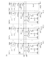
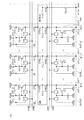
図1は、本発明の一態様の半導体装置である半導体装置10の構成例を示すブロック図である。半導体装置10は、表示装置11と、受信装置12と、を有する。また、図1には、放送信号を受信するアンテナANTと、半導体装置10の操作を行うリモコンRCと、を図示している。
FIG. 1 is a block diagram showing a configuration example of a
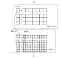
表示装置11は、表示部PAと、ゲートドライバ回路GDと、ソースドライバ回路SDと、タイミングコントローラTCと、AIデコーダAIDと、を有する。また、表示部PAには画素pixがx行y列(x、yは2以上の整数)のマトリクス状に配置されている。画素pixは、表示素子を有し、表示部PAが受信した画像データに対応する画像を当該表示素子により表示することができる。なお、表示部PAがカラー表示を行う場合、画素pixは、副画素を有する構成とすることができる。例えば、表示部PAが8Kの画像を3色(例えば、赤色、緑色、および青色)で表示する機能を有するとすると、表示部PAは画素pixを7680×4320個、副画素を7680×4320×3個有する。
The
本明細書等において、解像度という言葉は、表示部PAに設けられた画素pixの個数を示す。 In the present specification and the like, the term resolution indicates the number of pixel pix provided in the display unit PA.
受信装置12は、インターフェースI/F1と、デコーダDCDと、解像度拡張部DEと、画像処理部PPと、AIエンコーダAIEと、受信部RCVと、インターフェースI/F2と、制御部CPと、を有する。
The receiving
なお、半導体装置10において、表示装置11が有するAIデコーダAIDと、受信装置12が有するAIエンコーダAIEと、によって、オートエンコーダ13が構成されている。
In the
アンテナANTは、受信装置12のインターフェースI/F1と電気的に接続され、インターフェースI/F1は、デコーダDCDと電気的に接続されている。デコーダDCDは、解像度拡張部DEと電気的に接続され、解像度拡張部DEは、画像処理部PPと電気的に接続されている。画像処理部PPは、制御部CP、AIエンコーダAIE、およびタイミングコントローラTCと電気的に接続されている。受信部RCVは、インターフェースI/F2と電気的に接続され、インターフェースI/F2は、制御部CPと電気的に接続されている。制御部CPは、インターフェースI/F1、解像度拡張部DE、画像処理部PPおよびAIエンコーダAIEと電気的に接続され、AIエンコーダAIEは、AIデコーダAIDと電気的に接続されている。
The antenna ANT is electrically connected to the interface I / F1 of the receiving
AIデコーダAIDは、ソースドライバ回路SDと電気的に接続されている。タイミングコントローラTCは、ソースドライバ回路SDおよびゲートドライバ回路GDと電気的に接続されている。表示部PAは、ソースドライバ回路SDおよびゲートドライバ回路GDと電気的に接続されている。 The AI decoder AID is electrically connected to the source driver circuit SD. The timing controller TC is electrically connected to the source driver circuit SD and the gate driver circuit GD. The display unit PA is electrically connected to the source driver circuit SD and the gate driver circuit GD.
アンテナANTは、放送衛星、または電波塔等からの放送電波を受信して、電気信号に変換する機能を有する。また、アンテナANTは、該電気信号をインターフェースI/F1に送信する機能を有する。 The antenna ANT has a function of receiving a broadcast radio wave from a broadcasting satellite, a radio tower, or the like and converting it into an electric signal. Further, the antenna ANT has a function of transmitting the electric signal to the interface I / F1.
インターフェースI/F1は、該電気信号に含まれるチャンネルの信号を抽出して、放送信号として復調する機能を有する。なお、インターフェースI/F1は、アナログフロントエンドと呼ばれることがある。また、インターフェースI/F1は、当該放送信号を、デコーダDCDに送信する機能を有する。なお、放送信号をセットトップボックス(STB:Set Top Box)を介して入力する構成、録画再生機に録画したテレビ放送に対応したデータを入力する構成、ブルーレイ等の記録媒体に格納されたデータを入力する構成、等の各種構成とすることが可能である。これらの各種構成において、インターフェースI/F1として、HDMI(High−Definition Multimedia Interface)(登録商標)、SDI(Serial Digital Interface)等のデジタル信号インターフェースを用いることができる。なお、上記構成に各々対応したインターフェースを併設して、切り替えて利用する構成も可能である。以下、上記構成を都度説明することなく、アンテナで受信した放送信号を直接入力する構成を代表例として説明するが、各構成についても適宜読み替えることが可能である。 The interface I / F1 has a function of extracting a signal of a channel included in the electric signal and demodulating it as a broadcast signal. The interface I / F1 may be referred to as an analog front end. Further, the interface I / F1 has a function of transmitting the broadcast signal to the decoder DCD. In addition, a configuration in which a broadcast signal is input via a set top box (STB: Set Top Box), a configuration in which data corresponding to a television broadcast recorded in a recording / playback device is input, and data stored in a recording medium such as Blu-ray are input. It is possible to make various configurations such as an input configuration. In these various configurations, a digital signal interface such as HDMI (High-Definition Multimedia Interface) (registered trademark) or SDI (Serial Digital Interface) can be used as the interface I / F1. It is also possible to install an interface corresponding to each of the above configurations and switch between them. Hereinafter, a configuration in which a broadcast signal received by an antenna is directly input will be described as a typical example without explaining the above configuration each time, but each configuration can also be read as appropriate.
デコーダDCDは、放送信号に含まれる、画像データ、および音声データを復号伸長する機能を有する。特に、当該画像データは、画像データ21として、デコーダDCDから解像度拡張部DEに送信される。また、音声データは、半導体装置10が有する音声制御部、音声出力器等に送信される。なお、図1では、音声制御部、音声出力器は図示していない。
The decoder DCD has a function of decoding and decompressing image data and audio data contained in a broadcast signal. In particular, the image data is transmitted from the decoder DCD to the resolution expansion unit DE as the
解像度拡張部DEは、画像データ21を基にして、画像データ22を生成する機能を有する。画像データ22は、対応する画像の解像度を画像データ21より高めた画像データである。例えば、画像データ21に対応する画像の解像度を、2Kまたは4Kとし、画像データ22に対応する画像の解像度を、8Kとすることができる。また、画像データ22は、画素データの階調数を画像データ21に含まれる画素データより高めた画像データとすることができる。例えば、画像データ21に含まれる、画素データ1つあたりのビット数を1色あたり5ビットまたは6ビットとし、画像データ22に含まれる、画素データ1つあたりのビット数を1色あたり8ビットとすることができる。さらに、画像データ22は、画像の解像度を画像データ21より高め、かつ、画素データのビット数を画像データ21に含まれる画素データより高めた画像データとすることができる。例えば、画像データ21に対応する画像の解像度を2Kまたは4K、画素データ1つあたりのビット数を1色あたり5ビットまたは6ビットとし、画像データ22に対応する画像の解像度を8K、画素に含まれる画素データ1つあたりのビット数を1色あたり8ビットとすることができる。詳細は後述するが、解像度拡張部DEはニューラルネットワークを有し、当該ニューラルネットワークが学習を行うことにより、画像データ21から画像データ22を推論する機能を有することができる。画像データ22は、解像度拡張部DEから画像処理部PPに送信される。なお、画像データ22に対応する画像の解像度は、画像データ21に対応する画像の解像度のr倍(rは1より大きい実数)とすることができる。rは、2以上の整数とすることが好ましく、4のべき乗(4、16等)とすることがより好ましい。また、画像データ22に含まれる画素データ1つあたりの1色あたりのビット数は、画像データ21の画素データの1色あたりのビット数よりpビット高い(pは1以上の整数)とすることができる。なお、pは画像データ22に含まれる画素データの1色あたりのビット数の1/2より小さいことが好ましい。
The resolution expansion unit DE has a function of generating
画像処理部PPは、画像データ22に対して、各種画像処理を行う機能を有する。例えば、画像処理部PPは、ノイズ除去、ガンマ補正、調光、調色等を行うことができる。また、表示部PAに有機EL(Electro Luminescence)素子が含まれ、かつソースドライバ回路SDが当該有機EL素子に流れる電流を検出する電流検出回路を有する場合、画像処理部PPはEL補正を行うことができる。補正の施された画像データ22は、AIエンコーダAIEに送信される。
The image processing unit PP has a function of performing various image processing on the
AIエンコーダAIEは、受信した画像データ22を圧縮することにより、圧縮画像データ23を生成する機能を有する。AIデコーダAIDは、圧縮画像データ23を伸張することにより、画像データ22に復元する機能を有する。
The AI encoder AIE has a function of generating
また、AIデコーダAIDは、復元した画像データ22に含まれる画素データのビット数を増加させる、つまりビットアップを行う機能を有する。これにより、階調数を画像データ22より増加させた画像データである画像データ24を生成することができる。例えば、1つの画像データ22が、1色あたり6ビットの画素データを含む場合、画像データ24が含む画素データのビット数は、1色あたり8ビットとすることができる。この場合、AIデコーダAIDは、画像データの階調数を、64から256に増加させることができる。
Further, the AI decoder AID has a function of increasing the number of bits of pixel data included in the restored
なお、画像データ22に含まれる画素データ1つあたりのビット数は、画像データ24に含まれる画素データ1つあたりのビット数の1/2より多いことが好ましい。例えば、画像データ24に含まれる画素データ1つあたりのビット数が8ビットである場合、画像データ22に含まれる画素データ1つあたりのビット数は5ビット、6ビット、または7ビットであることが好ましい。また、画像データ22に含まれる画素データのビット数を増加させる場合、例えば画素データの下位ビットを増加させることができる。
The number of bits per pixel data included in the
以上より、オートエンコーダ13は、例えば画像データ22を圧縮、伸張し、さらにビットアップを行うことにより、階調数が画像データ22より多い画像データ24を生成する機能を有するということができる。
From the above, it can be said that the
なお、詳細は後述するが、オートエンコーダ13が有するニューラルネットワークが学習を行うことにより、画像データ22から画像データ24を推論する機能を有することができる。画像データ24は、AIデコーダAIDからソースドライバSDに送信することができる。
Although the details will be described later, the neural network of the
ユーザが半導体装置10を操作する手段として、リモコンRCを用いた方法がある。リモコンRCは、ユーザの操作によって、半導体装置10に対して制御信号を送ることができる。該制御信号とは、例えば、アンテナANTから受信した放送信号に含まれる各局の番組を選択する信号が挙げられる。また、該制御信号とは、例えば、表示装置11に表示される画像の色調、明るさ等を調節する信号も挙げられる。また、該制御信号とは、例えば、半導体装置10が画像データを録画および再生する機能を有する場合、当該画像データの再生、巻き戻し、早送り、停止等を行う信号等も挙げられる。また、該制御信号とは、例えば、インターフェースI/F1が複数のインターフェースを有する場合において、使用するインターフェースの選択を行う信号等も挙げられる。リモコンRCから送信する制御信号は、例えば、赤外線、または電波等がある。
As a means for the user to operate the
また、ユーザが半導体装置10を操作する手段は、図1の構成に限定せず、例えば、半導体装置10に備わる入力キー等によって、ユーザが直接半導体装置10を操作する方法とする構成としてもよい。
Further, the means for the user to operate the
受信部RCVは、リモコンRCからの制御信号を受信する機能を有する。受信部RCVは、該制御信号を受信することで、該制御信号をインターフェースI/F2に送信する機能を有する。 The receiving unit RCV has a function of receiving a control signal from the remote controller RC. The receiving unit RCV has a function of transmitting the control signal to the interface I / F2 by receiving the control signal.
インターフェースI/F2は、該制御信号を電気信号に変換して、制御部CPに送信する機能を有する。 The interface I / F2 has a function of converting the control signal into an electric signal and transmitting it to the control unit CP.
制御部CPは、インターフェースI/F2より送られた電気信号を解読する機能を有する。また、制御部CPは、当該電気信号に基づいて、解像度拡張部DE、画像処理部PP、およびオートエンコーダ13の重み係数の更新を行う機能を有する。また、制御部CPは、解像度拡張部DE、画像処理部PP、およびオートエンコーダ13における各種処理に必要なパラメータを変更する機能を有する。例えば、解像度拡張部DE、画像処理部PP、およびオートエンコーダ13がニューラルネットワークを有する構成の場合、各ニューラルネットワークの構成の変更を実行するために必要なデータを生成し、当該データを制御信号として解像度拡張部DE、画像処理部PP、およびオートエンコーダ13に送信する機能を有する。また、インターフェースI/F1が複数のインターフェースを有する場合、制御部CPは、インターフェースI/F2より送られた電気信号に基づいて、使用するインターフェースを選択する機能を有する。
The control unit CP has a function of decoding an electric signal sent from the interface I / F2. Further, the control unit CP has a function of updating the weighting coefficients of the resolution expansion unit DE, the image processing unit PP, and the
タイミングコントローラTCは、ソースドライバ回路SD、ゲートドライバ回路GDで使用するタイミング信号を生成する機能を有する。タイミング信号は、画像処理部PPから送信された画像データ22に含まれるフレームレート等を基に生成される。なお、当該タイミング信号は、画像処理部PPから送信された画像データ22のフレームレートに限定して生成されなくてもよい。
The timing controller TC has a function of generating a timing signal used in the source driver circuit SD and the gate driver circuit GD. The timing signal is generated based on the frame rate and the like included in the
ソースドライバ回路SDは、オートエンコーダ13が有するAIデコーダAIDから送信された画像データ24を受信する機能、および表示部PAに対して、画像データ24を送信する機能を有する。なお、当該画像データの表示部PAへの送信は、タイミングコントローラTCから送られるタイミング信号に基づいて行われる。
The source driver circuit SD has a function of receiving the
ゲートドライバ回路GDは、表示部PAが有する画素に対して、選択信号を送信する機能を有する。なお、選択信号の当該画素への送信は、タイミングコントローラTCから送られるタイミング信号に基づいて行われる。 The gate driver circuit GD has a function of transmitting a selection signal to the pixels of the display unit PA. The selection signal is transmitted to the pixel based on the timing signal transmitted from the timing controller TC.
表示装置11が有するAIデコーダAID、タイミングコントローラTC、ソースドライバ回路SD、およびゲートドライバ回路GDの少なくとも1つは、表示部PAが形成されている基板に、形成することができる。または、表示装置11が有するAIデコーダAID、タイミングコントローラTC、ソースドライバ回路SD、およびゲートドライバ回路GDの少なくとも1つは、IC(Integrated Circuit)として、表示部PAが形成されている基板に、COG(Chip On Glass)方式で実装することができる。または、表示装置11が有するAIデコーダAID、タイミングコントローラTC、ソースドライバ回路SD、およびゲートドライバ回路GDの少なくとも1つは、ICとして、表示部PAが形成されている基板に接続されているFPC(Frexible Print Circuit)に、COF(Chip On Film)方式で実装することができる。
At least one of the AI decoder AID, the timing controller TC, the source driver circuit SD, and the gate driver circuit GD of the
図2は、図1に示す半導体装置10の変形例であり、受信装置12が解像度拡張部DEをn個(nは2以上の整数)有する点、およびデコーダDCDが画像処理部PPと電気的に接続されている点が図1に示す構成の半導体装置10と異なる。図2等において、n個の解像度拡張部DEを、解像度拡張部DE[1]乃至解像度拡張部DE[n]と表記して区別する。
FIG. 2 is a modification of the
デコーダDCDおよび制御部CPは、解像度拡張部DE[1]乃至解像度拡張部DE[n]のそれぞれと電気的に接続されている。解像度拡張部DE[1]乃至解像度拡張部DE[n]は、順に直列に電気的に接続されており、解像度拡張部DE[n]は画像処理部PPと電気的に接続されている。 The decoder DCD and the control unit CP are electrically connected to each of the resolution expansion unit DE [1] to the resolution expansion unit DE [n]. The resolution expansion unit DE [1] to the resolution expansion unit DE [n] are electrically connected in series in order, and the resolution expansion unit DE [n] is electrically connected to the image processing unit PP.
インターフェースI/F1は、複数のインターフェースを有することができる。アンテナANTが受信した放送電波の種類に応じて、異なるインターフェースを使用することができる。例えば、インターフェースI/F1がSDIおよびHDMI(登録商標)を有する場合、アンテナANTが、8K放送に対応する放送電波を受信した場合はSDIを使用し、2K放送、4K放送等、その他8K放送以外の放送に対応する放送電波を受信した場合はHDMI(登録商標)を使用することができる。 The interface I / F1 can have a plurality of interfaces. Different interfaces can be used depending on the type of broadcast wave received by the antenna ANT. For example, when the interface I / F1 has SDI and HDMI (registered trademark), when the antenna ANT receives a broadcast radio wave corresponding to 8K broadcasting, SDI is used, 2K broadcasting, 4K broadcasting, etc., other than 8K broadcasting. HDMI (registered trademark) can be used when the broadcast radio wave corresponding to the broadcast of is received.
デコーダDCDは、アンテナANTが受信した放送電波の種類に応じて、異なる解像度拡張部DEに画像データ21を送信することができる。具体的には、アンテナANTが受信した放送電波が対応する解像度に応じて、解像度拡張部DE[1]乃至解像度拡張部DE[n]のいずれかに画像データ21を送信することができる。
The decoder DCD can transmit the
解像度拡張部DE[2]乃至解像度拡張部DE[n]は、デコーダDCDから受信した画像データ21の他、前の解像度拡張部DEが生成した画像データを基にして、対応する画像の解像度を高めた画像データを生成し、生成した画像データを次の解像度拡張部DEに送信する機能を有する。例えば、解像度拡張部DE[2]は、解像度拡張部[1]が生成した画像データを受信して、当該画像データより対応する画像の解像度が高い画像データを生成し、生成した画像データを解像度拡張部[3]に送信する機能を有する。また、例えば解像度拡張部DE[k](kは1以上n以下の整数)は、解像度拡張部[k−1]が生成した画像データを受信して、当該画像データより対応する画像の解像度が高い画像データを生成し、生成した画像データを解像度拡張部[k+1]に送信する機能を有する。なお、解像度拡張部DE[1]乃至解像度拡張部DE[n]は、受信した画像データに対してビットアップを行ってもよい。
The resolution expansion unit DE [2] to the resolution expansion unit DE [n] obtains the resolution of the corresponding image based on the
解像度拡張部DE[k]は、kの数が大きいほど、高解像度の画像に対応する画像データを受信し、より高解像度の画像に対応する画像データを生成することができる。例えば、n=2とする場合、解像度拡張部DE[1]は2Kに対応する画像の画像データを受信し、4Kの画像に対応する画像データを生成することができる。また、解像度拡張部DE[2]は4Kに対応する画像の画像データを受信し、8Kの画像に対応する画像データを生成することができる。以上により、低解像度の画像に対応する画像データ21を、解像度拡張部DE[1]乃至解像度拡張部DE[n]を用いて順次高解像度化することができる。例えば、2Kの画像に対応する画像データを、解像度拡張部DE[1]を用いて4Kの画像に対応する画像データとし、さらに解像度拡張部DE[2]を用いて8Kの画像に対応する画像データとすることができる。また、解像度拡張部DE[k]は、kの数が大きいほど、高階調数の画像に対応する画像データを受信し、より高階調数の画像に対応する画像データを生成することができる。
The resolution expansion unit DE [k] can receive image data corresponding to a high-resolution image and generate image data corresponding to a higher-resolution image as the number of k is larger. For example, when n = 2, the resolution expansion unit DE [1] can receive the image data of the image corresponding to 2K and generate the image data corresponding to the image of 4K. Further, the resolution expansion unit DE [2] can receive the image data of the image corresponding to 4K and generate the image data corresponding to the image of 8K. As described above, the
デコーダDCDは、アンテナANTが受信した放送電波が対応する解像度が、表示装置11が有する表示部PAに表示できる画像の解像度と等しい場合は、画像データ21を解像度拡張部DEに送信せず、画像データ21を画像データ22として直接画像処理部PPに送信することができる。例えば、表示装置11が有する表示部PAが8Kの画像を表示でき、アンテナANTが8K放送の放送電波を受信した場合は、画像データ21を画像データ22として直接画像処理部PPに送信することができる。
When the resolution corresponding to the broadcast radio wave received by the antenna ANT is equal to the resolution of the image that can be displayed on the display unit PA of the
半導体装置10を図2に示す構成とすることにより、例えば2K放送、4K放送、8K放送等、様々な種類の放送に対応する半導体装置10を提供することができる。
By configuring the
<画像処理部>
次に、画像処理部PPについて説明する。図3は、画像処理部PPの具体的な構成例を示すブロック図である。なお、図3には、画像処理部PPの他、解像度拡張部DEおよびAIエンコーダAIEも示している。
<Image processing unit>
Next, the image processing unit PP will be described. FIG. 3 is a block diagram showing a specific configuration example of the image processing unit PP. In addition to the image processing unit PP, FIG. 3 also shows the resolution expansion unit DE and the AI encoder AIE.
画像処理部PPは、画像処理回路PPC1と、画像認識回路PRCと、画像処理回路PPC2と、を有する。画像処理回路PPC1は、解像度拡張部DE、画像認識回路PRC、および画像処理回路PPC2と電気的に接続されている。画像認識回路PRCは、画像処理回路PPC2と電気的に接続されている。画像処理回路PPC2は、AIエンコーダAIEと電気的に接続されている。 The image processing unit PP includes an image processing circuit PPC1, an image recognition circuit PRC, and an image processing circuit PPC2. The image processing circuit PPC1 is electrically connected to the resolution expansion unit DE, the image recognition circuit PRC, and the image processing circuit PPC2. The image recognition circuit PRC is electrically connected to the image processing circuit PPC2. The image processing circuit PPC2 is electrically connected to the AI encoder AIE.
画像処理回路PPC1は、例えば画像処理フィルタとしての機能を有し、画像データ22に対しノイズ除去等の画像処理を行う機能を有する。画像処理回路PPC1は、ニューラルネットワークを有し、当該ニューラルネットワークの学習結果に応じて画像処理を行うことができる。
The image processing circuit PPC1 has, for example, a function as an image processing filter, and has a function of performing image processing such as noise removal on the
画像認識回路PRCは、画像データ22に対して特徴抽出を行い、画像データ22の属性を検出する機能を有する。画像認識回路PRCは、ニューラルネットワークを有し、当該ニューラルネットワークの学習結果に応じて画像データ22の属性を検出することができる。画像認識回路PRCにより検出された画像データ22の属性に関する情報(属性情報)は、画像処理回路PPC2に送信することができる。
The image recognition circuit PRC has a function of extracting features from the
画像処理回路PPC2は、画像認識回路PRCから受信した属性情報を基にして、画像データ22に対して画像処理を行う機能を有する。当該画像処理は、ガンマ補正等の補正処理等とすることができる。
The image processing circuit PPC2 has a function of performing image processing on the
<解像度拡張部>
次に、解像度拡張部DEについて説明する。図4は、解像度拡張部DEの構成例を示すブロック図である。前述のように、解像度拡張部DEは、ニューラルネットワークを有する。なお、図4では、解像度拡張部DEの他に、デコーダDCDおよび画像処理部PPも図示している。
<Resolution extension>
Next, the resolution expansion unit DE will be described. FIG. 4 is a block diagram showing a configuration example of the resolution expansion unit DE. As described above, the resolution extension unit DE has a neural network. In addition to the resolution expansion unit DE, FIG. 4 also shows the decoder DCD and the image processing unit PP.
解像度拡張部DEは、入力層IL1と、中間層ML1[1]と、中間層ML1[2]と、出力層OL1と、を有する。つまり、解像度拡張部DEでは、入力層IL1と、中間層ML1[1]と、中間層ML1[2]と、出力層OL1と、によって階層型のニューラルネットワークが構成されている。なお、階層型のニューラルネットワークの構成は、図4に示す解像度拡張部DEの有する中間層の数を増減した構成としてもよい。 The resolution expansion unit DE has an input layer IL1, an intermediate layer ML1 [1], an intermediate layer ML1 [2], and an output layer OL1. That is, in the resolution expansion unit DE, a hierarchical neural network is configured by the input layer IL1, the intermediate layer ML1 [1], the intermediate layer ML1 [2], and the output layer OL1. The hierarchical neural network may be configured by increasing or decreasing the number of intermediate layers included in the resolution expansion unit DE shown in FIG.
デコーダDCDから送信される画像データ21は、解像度拡張部DEの入力層IL1に入力される。つまり、画像データ21は、階層型のニューラルネットワークの入力データとして扱われる。また、解像度拡張部DEの出力層OL1からは、画像データ22が出力され、画像処理部PPに送信される。つまり、画像データ22は、階層型のニューラルネットワークの出力データとして扱われる。
The
解像度拡張部DEにおける階層型のニューラルネットワークは、階層が進む毎に、ニューロンの数が増加する構成とする。つまり、中間層ML1[1]が有するニューロンの数は、入力層IL1が有するニューロンの数より多く、かつ中間層ML1[2]が有するニューロンの数は、中間層ML1[1]が有するニューロンの数より多くなっている。また、出力層OL1が有するニューロンの数は、中間層ML1[2]が有するニューロンの数より多くなっている。なお、図4は、上記ニューロンの数を、それぞれの階層をつなぐ矢印の数で示している。解像度拡張部DEを、階調が進む毎にニューロンの数が増加する構成とすることにより、画像データ21を基にして、対応する画像の解像度を画像データ21より高めた画像データ22を生成することができる。また、画像データ21を基にして、階調数を画像データ21より高めた画像データ22を生成することができる。また、画像データ21を基にして、対応する画像の解像度、および階調数を画像データ21より高めた画像データ22を生成することができる。
The hierarchical neural network in the resolution expansion unit DE is configured such that the number of neurons increases as the hierarchy progresses. That is, the number of neurons in the middle layer ML1 [1] is larger than the number of neurons in the input layer IL1, and the number of neurons in the middle layer ML1 [2] is that of the neurons in the middle layer ML1 [1]. It's more than a number. Further, the number of neurons possessed by the output layer OL1 is larger than the number of neurons possessed by the intermediate layer ML1 [2]. In addition, FIG. 4 shows the number of the above-mentioned neurons by the number of arrows connecting each hierarchy. By configuring the resolution expansion unit DE so that the number of neurons increases as the gradation progresses,
解像度拡張部DEによって構成される階層型のニューラルネットワークでは、各層間で全結合とすることもでき、または、各層間で部分結合とすることができる。また、各層間に畳み込み層やプーリング層を用いた構成、すなわちCNNとすることができる。 In the hierarchical neural network configured by the resolution extension unit DE, it is possible to make a full connection between each layer or a partial connection between each layer. Further, it can be configured by using a convolutional layer or a pooling layer between each layer, that is, a CNN.
[解像度拡張部の学習方法の一例]
次に、解像度拡張部DEの学習方法の一例について説明する。解像度拡張部DEは、教師あり学習により学習を行うことができる。図5(A)、(B)、(C)は、解像度拡張部DEの学習方法の一例について説明するための図である。
[Example of learning method of resolution extension part]
Next, an example of the learning method of the resolution expansion unit DE will be described. The resolution extension unit DE can perform learning by supervised learning. 5A, 5B, and 5C are diagrams for explaining an example of a learning method of the resolution expansion unit DE.
まず、画像データ41を用意する。画像データ41は、例えば画像データ22に対応する画像の解像度と同じ解像度の画像を表し、かつ同じ階調数の画像データとすることができる。つまり、画像データ41は、表示部PAが表示する画像と同じ解像度の画像に対応し、かつ同じ階調数の画像データとすることができる。
First, the
画像データ41は、図5(A)に示すように、x行y列の画素データ51に分割することができる。つまり、画素データ51は、表示部PAが有する画素pixに対応する。画素データ51[b,a](aは1以上x以下の整数、bは1以上y以下の整数)は、例えば画素pix[b,a]により表現される階調を表す画素データとすることができる。
As shown in FIG. 5A, the
次に、s行t列分(s、tは2以上の整数。好ましくは、sはxの約数、tはyの約数)の画素データ51、例えば画素データ51[1,1]乃至画素データ51[t,s]を基にして、1つの画素データ52を生成する。1つの画素データ52は、1つの画素により表現される階調を表すデータとすることができる。画素データ52は、画素データ51[1,1]乃至画素データ51[t,s]の例えば平均値、最高値、または最低値等とすることができる。その後、画素データ51[1,1]乃至画素データ51[t,s]以外の画素データ51を基にして、同様の手順で画素データ52(s行t列分の画素データ51を基にしたデータ)を生成する。なお、画素データ52のビット数を、画素データ51のビット数より減少させてもよい。画素データのビット数を減少させる方法については後述する。
Next,
以上により、x/s行y/t列分の画素データ52を生成することができる。図5(B)に示すように、x/s行y/t列分の画素データ52をまとめて、画像データ42とする。
As a result, the
次に、画像データ41を教師データ、画像データ42を入力データとして、解像度変換部DEが学習を行う。具体的には、図5(C)に示すように、画像データ42から推論した画像データが画像データ41と一致するように、解像度拡張部DEの重み係数の更新等を行う。以上が解像度拡張部DEの学習方法の一例である。
Next, the resolution conversion unit DE performs learning using the
例えば、s=2、t=2とした場合、画像データ41に対応する画像の解像度を8Kとすると、画像データ42に対応する画像の解像度は4Kとなる。つまり、解像度拡張部DEは、4Kの画像に対応する画像データを基にして8Kの画像に対応する画像データを生成できるように、学習を行うことができる。また、例えば、s=4、t=4とした場合、画像データ41に対応する画像の解像度を8Kとすると、画像データ42に対応する画像の解像度は2Kとなる。つまり、解像度拡張部DEは、2Kの画像に対応する画像データを基にして8Kの画像に対応する画像データを生成できるように、学習を行うことができる。また、例えば画素データ51の1つあたりのビット数を1色あたり8ビット、画素データ52の1つあたりのビット数を1色あたり5ビットとすると、1色あたり5ビットの画素データを含む画像データを基にして、1色あたり8ビットの画素データを含む画像データを生成することができる。
For example, when s = 2 and t = 2, if the resolution of the image corresponding to the
なお、教師データである画像データ41を構成する画素データ51[1,1]乃至画素データ51[y,x]を全て一度に解像度変換部DEに入力すると、一度に入力されるデータ量が膨大となる。したがって、画素データ51[1,1]乃至画素データ51[y,x]の一部を入力して並列処理を行ってもよい。例えば、画素データ51[1,1]乃至画素データ51[y/2,x/2]と、画素データ51[1,x/2+1]乃至画素データ51[y/2,x]と、画素データ51[y/2+1,1]乃至画素データ51[y,x/2]と、画素データ51[y/2+1,x/2+1]乃至画素データ51[y,x]と、を別々に解像度変換部DEに入力し、並列に学習を行ってもよい。
If the pixel data 51 [1,1] to the pixel data 51 [y, x] constituting the
また、一部の画素データ51をオーバーラップさせて解像度変換部DEに入力してもよい。例えば、画素データ51[1,1]乃至画素データ51[y/2,x/2]と、画素データ51[1,x/2]乃至画素データ51[y/2,x]と、画素データ51[y/2,1]乃至画素データ51[y,x/2]と、画素データ51[y/2,x/2]乃至画素データ51[y,x]と、を別々に解像度変換部DEに入力する場合、画素データ51[1,x/2]乃至画素データ51[y,x/2]、および画素データ51[y/2,1]乃至画素データ51[y/2,x]を2回以上解像度変換部DEに入力することになる。これにより、解像度変換部DEが画像データ21を基にして画像データ22を生成する際の、画像データ22の精度を高めることができる。
Further, some
[解像度拡張部の動作方法の一例]
次に、解像度拡張部DEが学習を行った後に、解像度拡張部DEが動作を行う、つまり画像データ21を基に画像データ22を生成する場合における、解像度拡張部DEが動作方法の一例について説明する。図6は、解像度拡張部DEの動作方法の一例について説明するための図である。
[Example of how to operate the resolution expansion unit]
Next, an example of the operation method of the resolution expansion unit DE in the case where the resolution expansion unit DE operates after the resolution expansion unit DE learns, that is, the
画像データ21は、図6に示すように、x/s行y/t列分の画素データ31を含む。1つの画素データ31は、1つの画素により表現される階調を表すデータとすることができる。解像度拡張部DEは、学習結果を基にして、1つの画素データ31からs行t列分の画素データ32を生成する。つまり、解像度拡張部DEは、図6に示すように、x/s行y/t列分の画素データ31から、x行y列分の画素データ32を生成することができる。x行y列分の画素データ32をまとめて、画像データ22とすることができる。この場合、画素データ32[b,a]は、例えば画素pix[b,a]により表現される階調を表すデータとすることができる。
As shown in FIG. 6, the
以上により、解像度拡張部DEは、画像データ21を基にして、対応する画像の解像度が画像データ21のs×t倍である画像データ22を生成することができる。
As described above, the resolution expansion unit DE can generate
<オートエンコーダ>
次に、オートエンコーダ13について説明する。図7は、オートエンコーダ13の構成例を示すブロック図である。前述のように、オートエンコーダ13は、ニューラルネットワークを有する。なお、図7では、オートエンコーダ13の他に、画像処理部PPおよびソースドライバSDも図示している。
<Autoencoder>
Next, the
オートエンコーダ13が有するAIエンコーダAIEは、入力層IL2と、中間層ML2[1]と、中間層ML2[2]と、を有し、オートエンコーダ13が有するAIデコーダAIDは、中間層ML2[3]と、中間層ML2[4]と、中間層ML2[5]と、出力層OLと、を有する。つまり、オートエンコーダ13では、入力層IL2と、中間層ML2[1]乃至中間層ML2[5]と、出力層OL2と、によって階層型のニューラルネットワークが構成されている。なお、階層型のニューラルネットワークの構成は、図7に示すオートエンコーダ13の有する中間層の数を増減した構成としてもよい。
The AI encoder AIE included in the
画像処理部PPから送信される画像データ22は、オートエンコーダ13が有するAIエンコーダAIEの入力層IL2に入力される。つまり、画像データ22は、階層型のニューラルネットワークの入力データとして扱われる。また、AIデコーダAIDの出力層OL2からは、画像データ24が出力され、ソースドライバ回路SDに送信される。つまり、画像データ22は、階層型のニューラルネットワークの出力データとして扱われる。
The
AIエンコーダAIEにおける階層型のニューラルネットワークは、階層が進む毎に、ニューロンの数が減少する構成とする。つまり、中間層ML2[1]が有するニューロンの数は、入力層IL2が有するニューロンの数よりも少なく、かつ中間層ML2[2]が有するニューロンの数は、中間層ML2[1]が有するニューロンの数よりも少なくなっている。なお、図7は、上記ニューロンの数を、それぞれの階層をつなぐ矢印の数で示している。 The hierarchical neural network in the AI encoder AIE is configured such that the number of neurons decreases as the hierarchy progresses. That is, the number of neurons in the middle layer ML2 [1] is smaller than the number of neurons in the input layer IL2, and the number of neurons in the middle layer ML2 [2] is the number of neurons in the middle layer ML2 [1]. Is less than the number of. In addition, FIG. 7 shows the number of the above-mentioned neurons by the number of arrows connecting each hierarchy.
AIデコーダAIDにおける階層型のニューラルネットワークは、階層が進む毎に、ニューロンの数が増加する構成とする。つまり、中間層ML2[4]が有するニューロンの数は、中間層ML2[3]が有するニューロンの数よりも多く、かつ中間層ML2[5]が有するニューロンの数は、中間層ML2[4]が有するニューロンの数よりも多くなっている。また、出力層OL2が有するニューロンの数は、中間層ML2[5]が有するニューロンの数よりも多くなっている。 The hierarchical neural network in the AI decoder AID is configured such that the number of neurons increases as the hierarchy progresses. That is, the number of neurons in the middle layer ML2 [4] is larger than the number of neurons in the middle layer ML2 [3], and the number of neurons in the middle layer ML2 [5] is the number of neurons in the middle layer ML2 [4]. Has more neurons than it has. Further, the number of neurons possessed by the output layer OL2 is larger than the number of neurons possessed by the intermediate layer ML2 [5].
AIデコーダAIDが有する中間層の数は、AIエンコーダAIEが有する中間層の数より多くすることが好ましい。これにより、オートエンコーダ13は、画像データ22の階調数を増加させる機能を有することができる。なお、AIデコーダAIDが有するニューロン数、重み係数のビット数、重み係数の数等をAIエンコーダAIEより多くするのであれば、AIデコーダAIDが有する中間層の数が、AIエンコーダAIEが有する中間層の数以下であってもよい。
The number of intermediate layers possessed by the AI decoder AID is preferably larger than the number of intermediate layers possessed by the AI encoder AIE. As a result, the
なお、オートエンコーダ13によって構成される階層型のニューラルネットワークでは、各層間で全結合とすることもでき、または、各層間で部分結合とすることができる。また、各層間に畳み込み層やプーリング層を用いた構成、すなわちCNNとすることができる。
In the hierarchical neural network configured by the
[オートエンコーダの学習方法および動作方法の一例]
次に、オートエンコーダ13の学習方法、および学習後の動作方法の一例について説明する。オートエンコーダ13は、教師あり学習により学習を行うことができる。
[Example of autoencoder learning method and operation method]
Next, an example of the learning method of the
上記教師あり学習において、教師データは、画像データ24に含まれる画素データのビット数と同じビット数の画素データを含む画像データとする。つまり、表示部PAに送信される画像データに含まれる画素データのビット数と同じビット数の画素データを含む画像データを教師データとする。
In the supervised learning, the teacher data is image data including pixel data having the same number of bits as the number of bits of the pixel data included in the
入力データは、教師データに含まれる画素データのビット数を減らすことにより生成することができる。例えば、教師データに含まれる各画素データの下位ビットを削ることにより、入力データを生成することができる。なお、削るビット数は、教師データに含まれるビット数の1/2より少ないことが好ましい。例えば、教師データに含まれる画素データ1つあたりのビット数が、1色あたり8ビットである場合、各画素データの下位ビットを1色ごとに1ビットずつ、2ビットずつ、または3ビットずつ削ることにより、入力データを生成することが好ましい。なお、解像度拡張部DEが学習を行う場合においても、同様の手順で、入力データである画像データ42に含まれる画素データ52のビット数を、教師データである画像データ41に含まれる画素データ51のビット数より減少させることができる。
The input data can be generated by reducing the number of bits of the pixel data included in the teacher data. For example, input data can be generated by removing the lower bits of each pixel data included in the teacher data. The number of bits to be deleted is preferably less than 1/2 of the number of bits included in the teacher data. For example, when the number of bits per pixel data included in the teacher data is 8 bits per color, the lower bits of each pixel data are deleted by 1 bit, 2 bits, or 3 bits for each color. Therefore, it is preferable to generate input data. Even when the resolution expansion unit DE performs learning, the number of bits of the
オートエンコーダ13は、入力データから推論した画像データが教師データに一致するように学習、例えばオートエンコーダ13の重み係数の更新等を行う。以上がオートエンコーダ13の学習方法の一例である。
The
オートエンコーダ13が学習を行った後に、オートエンコーダ13に画像データ22が送信されると、オートエンコーダ13は学習結果を基にして、階調数を画像データ22より増加させた画像データ24を生成することができる。以上がオートエンコーダ13の動作方法の一例である。
When the
本実施の形態は、本明細書で示す他の実施の形態と適宜組み合わせることができる。 This embodiment can be appropriately combined with other embodiments shown herein.
(実施の形態2)
本実施の形態では、階層型のニューラルネットワークと、当該ニューラルネットワークに適用できる積和演算回路の構成例について説明する。
(Embodiment 2)
In this embodiment, a hierarchical neural network and a configuration example of a product-sum operation circuit applicable to the neural network will be described.
<階層型のニューラルネットワーク>
本発明の一態様の半導体装置に利用できるニューラルネットワークの種類の一として、階層型のニューラルネットワークについて説明する。
<Hierarchical neural network>
A hierarchical neural network will be described as one of the types of neural networks that can be used in the semiconductor device of one aspect of the present invention.
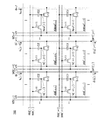
図8は、階層型のニューラルネットワークの一例を示した図である。第(k−1)層(ここでのkは2以上の整数である。)は、ニューロンをP個(ここでのPは1以上の整数である。)有し、第k層は、ニューロンをQ個(ここでのQは1以上の整数である。)有し、第(k+1)層は、ニューロンをR個(ここでのRは1以上の整数である。)有する。 FIG. 8 is a diagram showing an example of a hierarchical neural network. The layer (k-1) (where k is an integer of 2 or more) has P neurons (where P is an integer of 1 or more), and the layer k is a neuron. (Q here is an integer of 1 or more), and the layer (k + 1) has R neurons (R here is an integer of 1 or more).
第(k−1)層の第pニューロン(ここでのpは1以上P以下の整数である。)の出力信号zp (k−1)と重み係数wqp (k)と、の積が第k層の第qニューロン(ここでのqは1以上Q以下の整数である。)に入力されるものとし、第k層の第qニューロンの出力信号zq (k)と重み係数wrq (k+1)と、の積が第(k+1)層の第rニューロン(ここでのrは1以上R以下の整数である。)に入力されるものとし、第(k+1)層の第rニューロンの出力信号をzr (k+1)とする。 And the (p-here is an integer of 1 or more P.) (K-1) p th neuron of the layer output signal z p (k-1) and the weighting coefficient w qp of (k), the product of It is assumed that it is input to the qth neuron of the kth layer (q here is an integer of 1 or more and Q or less), and the output signal z q (k) and the weighting coefficient w rq of the qth neuron of the kth layer. It is assumed that the product of (k + 1) and is input to the r-neuron of the (k + 1) layer (where r is an integer of 1 or more and R or less), and the r-neuron of the (k + 1) layer. Let the output signal be zr (k + 1) .
このとき、第k層の第qニューロンへ入力される信号の総和は、次の式で表される。 At this time, the sum of the signals input to the qth neuron in the kth layer is expressed by the following equation.

また、第k層の第qニューロンからの出力信号zq (k)を次の式で定義する。 Further, the output signal z q (k) from the qth neuron in the kth layer is defined by the following equation.
関数f(uq (k))は、活性化関数であり、ステップ関数、線形ランプ関数、またはシグモイド関数等を用いることができる。なお、式(D1)の積和演算は、後述する積和演算回路700によって実現できる。なお、式(D2)の演算は、例えば、図11(A)に示す回路161によって実現できる。
The function f (u q (k) ) is an activation function, and a step function, a linear ramp function, a sigmoid function, or the like can be used. The product-sum calculation of the equation (D1) can be realized by the product-
なお、活性化関数は、全てのニューロンにおいて同一でもよいし、または異なっていてもよい。加えて、活性化関数は、層毎において、同一でもよいし、異なっていてもよい。 The activation function may be the same or different in all neurons. In addition, the activation function may be the same or different for each layer.
ここで、図9に示す、全L層からなる階層型のニューラルネットワークを考える(つまり、ここでのkは2以上(L−1)以下の整数とする。)。第1層は、階層型のニューラルネットワークの入力層となり、第L層は、階層型のニューラルネットワークの出力層となり、第2層乃至第(L−1)層は、隠れ層となる。 Here, consider a hierarchical neural network consisting of all L layers shown in FIG. 9 (that is, k here is an integer of 2 or more (L-1) or less). The first layer is an input layer of a hierarchical neural network, the L layer is an output layer of a hierarchical neural network, and the second layer to the (L-1) layer are hidden layers.
第1層(入力層)は、ニューロンをP個有し、第k層(隠れ層)は、ニューロンをQ[k]個(Q[k]は1以上の整数である。)有し、第L層(出力層)は、ニューロンをR個有する。 The first layer (input layer) has P neurons, and the kth layer (hidden layer) has Q [k] neurons (Q [k] is an integer of 1 or more). The L layer (output layer) has R neurons.
第1層の第s[1]ニューロン(s[1]は1以上P以下の整数である。)の出力信号をzs[1] (1)とし、第k層の第s[k]ニューロン(s[k]は1以上Q[k]以下の整数である。)の出力信号をzs[k] (k)とし、第L層の第s[L]ニューロン(s[L]は1以上R以下の整数である。)の出力信号をzs[L] (L)とする。 Let z s [1] (1) be the output signal of the first layer s [1] neuron (s [1] is an integer of 1 or more and P or less), and the kth layer s [k] neuron. The output signal of (s [k] is an integer of 1 or more and Q [k] or less) is z s [k] (k), and the s [L] neuron (s [L] of the Lth layer is 1). Let z s [L] (L) be the output signal of (which is an integer less than or equal to R).
また、第(k−1)層の第s[k−1]ニューロン(s[k−1]は1以上Q[k−1]以下の整数である。)の出力信号zs[k−1] (k−1)と重み係数ws[k]s[k−1] (k)と、の積us[k] (k)が第k層の第s[k]ニューロンに入力されるものとし、第(L−1)層の第s[L−1]ニューロン(s[L−1]は1以上Q[L−1]以下の整数である。)の出力信号zs[L−1] (L−1)と重み係数ws[L]s[L−1] (L)と、の積us[L] (L)が第L層の第s[L]ニューロンに入力されるものとする。 Further, the output signal z s [k-1 ] of the s [k-1] neuron of the layer (k-1) (s [k-1] is an integer of 1 or more and Q [k-1] or less). ] (K-1) and the weighting coefficient w s [k] s [k-1] (k) , the product us [k] (k) is input to the kth layer s [k] neuron. The output signal z s [L- ] of the s [L-1] neuron of the layer (L-1) (s [L-1] is an integer of 1 or more and Q [L-1] or less). 1] The product us [L] (L) of (L-1) and the weighting coefficient w s [L] s [L-1] (L) is input to the s [L] neuron of the Lth layer. It shall be.
次に、教師あり学習について説明する。教師あり学習とは、上述の階層型のニューラルネットワークの機能において、出力した結果と、所望の結果(教師データ、または教師信号という場合がある。)と異なったときに、階層型のニューラルネットワークの全ての重み係数を、出力した結果と所望の結果とに基づいて、更新する動作をいう。 Next, supervised learning will be described. Supervised learning is a function of a hierarchical neural network described above, in which the output result differs from a desired result (sometimes referred to as teacher data or a teacher signal). The operation of updating all the weighting coefficients based on the output result and the desired result.
教師あり学習の具体例として、逆伝播誤差方式による学習方法について説明する。図10は、逆伝播誤差方式による学習方法を説明する図である。逆伝播誤差方式は、階層型のニューラルネットワークの出力と教師データとの誤差が小さくなるに、重み係数を変更する方式である。 As a specific example of supervised learning, a learning method using the back propagation error method will be described. FIG. 10 is a diagram illustrating a learning method by the back propagation error method. The back propagation error method is a method of changing the weighting coefficient so that the error between the output of the hierarchical neural network and the teacher data becomes small.
例えば、第1層の第s[1]ニューロンに入力データを入力し、第L層の第s[L]ニューロンから出力データzs[L] (L)を出力されたとする。ここで、出力データzs[L] (L)に対する教師信号をts[L]としたとき、誤差エネルギーEは、出力データzs[L] (L)および教師信号ts[L]によって表すことができる。 For example, it is assumed that the input data is input to the s [1] neuron of the first layer and the output data z s [L] (L) is output from the s [L] neuron of the L layer. Here, when the teacher signal for the output data z s [L] (L) is t s [L] , the error energy E is determined by the output data z s [L] (L) and the teacher signal t s [L] . Can be represented.
誤差エネルギーEに対して、第k層の第s[k]ニューロンの重み係数ws[k]s[k−1] (k)の更新量を∂E/∂ws[k]s[k−1] (k)とすることで、新たに重み係数を変更することができる。ここで、第k層の第s[k]ニューロンの出力値zs[k] (k)の誤差δs[k] (k)を∂E/∂us[k] (k)と定義すると、δs[k] (k)および∂E/∂ws[k]s[k−1] (k)は、それぞれ次の式で表すことができる。 With respect to the error energy E, the update amount of the weighting coefficient w s [k] s [k-1] (k) of the kth layer kth neuron is ∂E / ∂w s [k] s [k. -1] By setting (k) , the weighting coefficient can be newly changed. Here, if the error δ s [k] (k) of the output value z s [k] (k) of the kth layer kth neuron is defined as ∂E / ∂u s [k] (k). , Δ s [k] (k) and ∂E / ∂w s [k] s [k-1] (k) can be expressed by the following equations, respectively.
f’(us[k] (k))は、ニューロン回路の出力関数の導関数である。なお、式(D3)の演算は、例えば、図11(B)に示す回路163によって実現できる。また、式(D4)の演算は、例えば、図11(C)に示す回路164によって実現できる。出力関数の導関数は、例えば、オペアンプの出力端子に所望の導関数に対応した演算回路を接続することによって実現できる。
f'(us [k] (k) ) is a derivative of the output function of the neuron circuit. The calculation of the equation (D3) can be realized by, for example, the circuit 163 shown in FIG. 11 (B). Further, the calculation of the equation (D4) can be realized by, for example, the
また、例えば、式(D3)のΣws[k+1]・s[k] (k+1)・δs[k+1] (k+1)の部分の演算は、後述する積和演算回路700によって実現できる。
Further, for example, the calculation of the Σw s [k + 1], s [k] (k + 1) , δ s [k + 1] (k + 1) portion of the equation (D3) can be realized by the multiply-accumulate
ここで、第(k+1)層が出力層のとき、すなわち、第(k+1)層が第L層であるとき、δs[L] (L)および∂E/∂ws[L]s[L−1] (L)は、それぞれ次の式で表すことができる。 Here, when the first (k + 1) layer is the output layer, that is, when the first (k + 1) layer is the Lth layer, δ s [L] (L) and ∂E / ∂w s [L] s [L. -1] (L) can be expressed by the following equations, respectively.
式(D5)の演算は、図11(D)に示す回路165によって実現できる。また、式(D6)の演算は、図11(C)に示す回路164によって実現できる。
The operation of the equation (D5) can be realized by the
つまり、式(D1)乃至式(D6)により、全てのニューロン回路の誤差δs[k] (k)およびδs[L] (L)を求めることができる。なお、重み係数の更新は、誤差δs[k] (k)、δs[L] (L)および所望のパラメータ等に基づいて、設定される。 That is, the errors δ s [k] (k) and δ s [L] (L) of all the neuron circuits can be obtained from the equations (D1) to (D6). The update of the weighting coefficient is set based on the error δ s [k] (k) , δ s [L] (L), a desired parameter, and the like.
以上のように、図11(A)乃至図11(D)に示す回路、および後述する積和演算回路700を用いることによって、教師あり学習を適用した階層型のニューラルネットワークの計算を行うことができる。
As described above, by using the circuits shown in FIGS. 11A to 11D and the multiply-accumulate
<階層型ニューラルネットワークの回路構成例>
図12は、階層型ニューラルネットワークの回路の構成例を示したブロック図である。
<Circuit configuration example of hierarchical neural network>
FIG. 12 is a block diagram showing a configuration example of a circuit of a hierarchical neural network.
NN(ニューラルネットワーク)回路100は、入力端子PDL[1]乃至入力端子PDL[l](ここでのlは1以上の整数である。)、出力端子PDR[1]乃至出力端子PDR[n](ここでのnは1以上の整数である。)、プログラマブルロジックエレメントPLE[1]乃至プログラマブルロジックエレメントPLE[m]、配線L[1]乃至配線L[l]、配線P[1]乃至配線P[m]、配線R[1]乃至配線R[n]、配線Q[1]乃至配線Q[m]、複数のプログラマブルスイッチPSW1、複数のプログラマブルスイッチPSW2、および複数のプログラマブルスイッチPSW3を有する。
The NN (neural network)
なお、図12に示すNN回路100では、入力端子PDL[1]、入力端子PDL[2]、入力端子PDL[l]、出力端子PDR[1]、出力端子PDR[2]、出力端子PDR[n]、プログラマブルロジックエレメントPLE[1]、プログラマブルロジックエレメントPLE[2]、プログラマブルロジックエレメントPLE[m]、配線L[1]、配線L[2]、配線L[l]、配線P[1]、配線P[2]、配線P[m]、配線R[1]、配線R[2]、配線R[n]、配線Q[1]、配線Q[2]、配線Q[m]、プログラマブルスイッチPSW1、プログラマブルスイッチPSW2、プログラマブルスイッチPSW3、後述するスイッチ回路SWCのみを図示しており、それら以外の回路、素子、配線、符号を省略している。
In the
つまり、本発明の一態様は、プログラマブルロジックエレメントPLE[1]乃至プログラマブルロジックエレメントPLE[m]、およびプログラマブルスイッチPSW1乃至プログラマブルスイッチPSW3を用いた、マルチコンテキスト方式のプログラマブルな演算処理装置である。具体的には後述するが、当該演算処理装置は、階層型のニューラルネットワークにおいて、各階層間のネットワークの接続状態を各コンテキストに対応させており、コンテキストを順次切り替えることによって、ニューラルネットワークの演算処理を行う。 That is, one aspect of the present invention is a multi-context programmable arithmetic processing device using a programmable logic element PLE [1] to a programmable logic element PLE [m] and a programmable switch PSW1 to a programmable switch PSW3. Specifically, as will be described later, in the hierarchical neural network, the operation processing device corresponds to each context in the connection state of the network between each layer, and the arithmetic processing of the neural network is performed by sequentially switching the contexts. I do.
入力端子PDL[i](ここでのiは1以上l以下の整数である。)は、配線L[i]と電気的に接続されている。出力端子PDR[k](ここでのkは1以上n以下の整数である。)は、配線R[1]乃至配線R[n]のそれぞれと、プログラマブルスイッチPSW3を介して、電気的に接続されている。プログラマブルロジックエレメントPLE[j](ここでのjは1以上m以下の整数である。)の第1端子は、配線Q[j]と電気的に接続され、配線Q[j]は、配線L[1]乃至配線L[l]のそれぞれと、プログラマブルスイッチPSW2を介して、電気的に接続されている。また、配線Q[j]は、配線P[1]乃至配線P[m]のそれぞれと、プログラマブルスイッチPSW1を介して、電気的に接続されている。プログラマブルロジックエレメントPLE[j]の第2端子は、配線R[j]と電気的に接続されている。配線P[1]乃至P[m]のそれぞれは、配線R[1]乃至R[n]のそれぞれと電気的に接続されている。 The input terminal PDL [i] (where i is an integer of 1 or more and less than or equal to l) is electrically connected to the wiring L [i]. The output terminal PDR [k] (k here is an integer of 1 or more and n or less) is electrically connected to each of the wiring R [1] to the wiring R [n] via the programmable switch PSW3. Has been done. The first terminal of the programmable logic element PLE [j] (where j is an integer of 1 or more and m or less) is electrically connected to the wiring Q [j], and the wiring Q [j] is the wiring L. It is electrically connected to each of [1] to the wiring L [l] via the programmable switch PSW2. Further, the wiring Q [j] is electrically connected to each of the wiring P [1] to the wiring P [m] via the programmable switch PSW1. The second terminal of the programmable logic element PLE [j] is electrically connected to the wiring R [j]. Each of the wirings P [1] to P [m] is electrically connected to each of the wirings R [1] to R [n].
NN回路100が有するプログラマブルスイッチPSW1乃至プログラマブルスイッチPSW3は、後述するコンフィギュレーションメモリCMSに格納されたコンフィギュレーションデータによって、導通状態、非導通状態を切り替えることができるスイッチである。なお、プログラマブルスイッチPSW1乃至プログラマブルスイッチPSW3のそれぞれは、スイッチ回路SWCを有する。また、プログラマブルスイッチPSW1乃至プログラマブルスイッチPSW3の詳細については、後述する。
The programmable switch PSW1 to the programmable switch PSW3 included in the
プログラマブルロジックエレメントPLEは、図13(A)に示す演算処理回路を有する。演算処理回路150は、入力端子In[1]乃至入力端子In[s](ここでのsは1以上の整数である。)と、出力端子OUTと、乗算回路MLT[1]乃至乗算回路MLT[s]と、加算回路ADと、活性化関数回路AFC と、保持回路KCと、コンフィギュレーションメモリCMW[1]乃至コンフィギュレーションメモリCMW[s]と、コンフィギュレーションメモリCMFと、を有する。なお、コンフィギュレーションメモリCMW[1]乃至コンフィギュレーションメモリCMW[s]は一つのコンフィギュレーションメモリとしてもよい。また、コンフィギュレーションメモリCMW[1]乃至コンフィギュレーションメモリCMW[s]と、コンフィギュレーションメモリCMFと、は一つのコンフィギュレーションメモリとしてもよい。
The programmable logic element PLE has an arithmetic processing circuit shown in FIG. 13 (A). The
入力端子In[h](ここでのhは1以上s以下の整数である。)は、乗算回路MLT[h]の入力端子と電気的に接続され、乗算回路MLT[h]の出力端子は、加算回路ADの入力端子と電気的に接続されている。加算回路ADの出力端子は、活性化関数回路AFC の入力と電気的に接続されている。活性化関数回路AFC の出力端子は、保持回路KCの端子TA1と電気的に接続されている。保持回路KCの端子TA2は、出力端子OUTと電気的に接続されている。 The input terminal In [h] (h here is an integer of 1 or more and s or less) is electrically connected to the input terminal of the multiplication circuit MLT [h], and the output terminal of the multiplication circuit MLT [h] is , It is electrically connected to the input terminal of the adder circuit AD. The output terminal of the adder circuit AD is electrically connected to the input of the activation function circuit AFC. The output terminal of the activation function circuit AFC is electrically connected to the terminal TA1 of the holding circuit KC. The terminal TA2 of the holding circuit KC is electrically connected to the output terminal OUT.
乗算回路MLT[h]は、コンフィギュレーションメモリCMW[h]に保持されているデータ(以後、重み係数と呼称する。)を乗数とし、入力端子In[h]に入力された入力信号を被乗数とする乗算を行う回路である。加算回路ADは、乗算回路MLT[1]乃至乗算回路MLT[s]から出力されるそれぞれの乗算結果の和を計算する回路である。つまり、乗算回路MLT[1]乃至乗算回路MLT[s]、および加算回路ADによって、積和演算回路が構成されている。 The multiplication circuit MLT [h] uses the data held in the configuration memory CMW [h] (hereinafter referred to as a weighting coefficient) as a multiplier, and the input signal input to the input terminal In [h] as a multiplier. It is a circuit that performs multiplication. The addition circuit AD is a circuit that calculates the sum of the multiplication results output from the multiplication circuit MLT [1] to the multiplication circuit MLT [s]. That is, the product-sum calculation circuit is configured by the multiplication circuit MLT [1] to the multiplication circuit MLT [s] and the addition circuit AD.
活性化関数回路AFC は、入力端子に入力された信号、つまり積和演算結果に対して、コンフィギュレーションメモリCMFに保持されているデータにより定義された関数系に従った演算を行う回路である。当該関数系としては、例えば、シグモイド関数、tanh関数、softmax関数、ReLU関数、しきい値関数等を用いることができる。 The activation function circuit AFC is a circuit that performs an operation on a signal input to an input terminal, that is, a product-sum operation result, according to a function system defined by data held in the configuration memory CMF. As the function system, for example, a sigmoid function, a tanh function, a softmax function, a ReLU function, a threshold value function, or the like can be used.
保持回路KCは、活性化関数回路AFC から出力された演算結果を端子TA1から取得し、当該演算結果を一時的に保持する機能と、一時的に保持した演算結果を端子TA2に出力する機能とを有する。加えて、保持回路KCは、端子CKTに入力されるクロック信号CLKに応じて、上述した2つの機能を切り替えることができる。 The holding circuit KC has a function of acquiring the calculation result output from the activation function circuit AFC from the terminal TA1 and temporarily holding the calculation result, and a function of outputting the temporarily held calculation result to the terminal TA2. Have. In addition, the holding circuit KC can switch between the above two functions according to the clock signal CLK input to the terminal CKT.
例えば、クロック信号CLKが高レベル電位であるとき、保持回路KCは、端子TA1から入力された電位を保持することができ、クロック信号CLKが低レベル電位であるとき、保持回路KCは、端子TA2から出力端子OUTに、該電位を出力することができる。 For example, when the clock signal CLK has a high level potential, the holding circuit KC can hold the potential input from the terminal TA1, and when the clock signal CLK has a low level potential, the holding circuit KC has the terminal TA2. The potential can be output from the output terminal OUT to the output terminal OUT.
演算処理回路150はデジタルデータを扱う回路である場合、保持回路KCは、例えば、フリップフロップ回路を適用することができる。
When the
また、演算処理回路150はアナログデータを扱う回路である場合、一例として、図13(B)に示す保持回路KCを適用することができる。図13(B)に示す保持回路KCは、サンプルホールド回路であり、トランジスタTrAと、トランジスタTrBと、容量素子CAと、アンプAMPと、NOT回路NLと、を有する。
Further, when the
トランジスタTrAの第1端子は、端子TA1と電気的に接続され、トランジスタTrAの第2端子は、容量素子CAの第1端子と電気的に接続され、トランジスタTrAのゲートは、端子CKTと電気的に接続されている。アンプAMPの入力端子は、トランジスタTrの第2端子と電気的に接続され、アンプAMPの出力端子は、トランジスタTrBの第1端子と電気的に接続されている。トランジスタTrBの第2端子は、端子TA2と電気的に接続されている。NOT回路NLの入力端子は、端子CKTと電気的に接続され、NOT回路NLの出力端子は、トランジスタTrBのゲートと電気的に接続されている。容量素子CAの第2端子は、配線GNDと電気的に接続されている。なお、トランジスタTrAの第2端子と、アンプAMPの入力端子と、容量素子の第1端子の接続点を、ノードNとする。 The first terminal of the transistor TrA is electrically connected to the terminal TA1, the second terminal of the transistor TrA is electrically connected to the first terminal of the capacitive element CA, and the gate of the transistor TrA is electrically connected to the terminal CKT. It is connected to the. The input terminal of the amplifier AMP is electrically connected to the second terminal of the transistor Tr, and the output terminal of the amplifier AMP is electrically connected to the first terminal of the transistor TrB. The second terminal of the transistor TrB is electrically connected to the terminal TA2. The input terminal of the NOT circuit NL is electrically connected to the terminal CKT, and the output terminal of the NOT circuit NL is electrically connected to the gate of the transistor TrB. The second terminal of the capacitive element CA is electrically connected to the wiring GND. The connection point between the second terminal of the transistor TrA, the input terminal of the amplifier AMP, and the first terminal of the capacitive element is defined as a node N.
アンプAMPは、入力端子に入力された信号を1倍に増幅して、出力端子に増幅した信号を出力する機能を有する。 The amplifier AMP has a function of amplifying the signal input to the input terminal by 1 time and outputting the amplified signal to the output terminal.
配線GNDは、基準電位を与える配線である。 The wiring GND is a wiring that gives a reference potential.
端子CKTに入力されるクロック信号CLKが高レベル電位であるとき、トランジスタTrAは導通状態となり、トランジスタTrBは非導通状態となる。このとき、端子TA1から入力された信号は、トランジスタTrAを介して、アンプAMPに入力される。このため、アンプAMPは該信号を増幅して、アンプAMPの出力端子から増幅した信号を出力する。なお、トランジスタTrBは非導通状態であるため、増幅した信号は、端子TA2から出力されない。 When the clock signal CLK input to the terminal CKT has a high level potential, the transistor TrA is in a conductive state, and the transistor TrB is in a non-conducting state. At this time, the signal input from the terminal TA1 is input to the amplifier AMP via the transistor TrA. Therefore, the amplifier AMP amplifies the signal and outputs the amplified signal from the output terminal of the amplifier AMP. Since the transistor TrB is in a non-conducting state, the amplified signal is not output from the terminal TA2.
また、ノードNの電位は、容量素子CAによって、保持される。このとき、ノードNの電位は、端子TA1から入力された信号の電位となる。 Further, the potential of the node N is held by the capacitive element CA. At this time, the potential of the node N becomes the potential of the signal input from the terminal TA1.
端子CKTに入力されるクロック信号CLKが低レベル電位であるとき、トランジスタTrAは非導通状態となり、トランジスタTrBは導通状態となる。ノードNの電位は、トランジスタTrAが非導通状態となっているので、該電位の変化はない。アンプAMPは、ノードNの電位をトランジスタTrBの第1端子に出力をする。トランジスタTrBは導通状態となっているため、ノードNの電位、つまりクロック信号CLKが高レベル電位のときに端子TA1から入力された信号の電位が、端子TA2から出力される。 When the clock signal CLK input to the terminal CKT has a low level potential, the transistor TrA is in a non-conducting state, and the transistor TrB is in a conducting state. Since the transistor TrA is in a non-conducting state, the potential of the node N does not change. The amplifier AMP outputs the potential of the node N to the first terminal of the transistor TrB. Since the transistor TrB is in a conductive state, the potential of the node N, that is, the potential of the signal input from the terminal TA1 when the clock signal CLK is a high level potential is output from the terminal TA2.
トランジスタTrA、および/またはトランジスタTrBは、実施の形態4で説明するOSトランジスタであることが好ましい。特に、該OSトランジスタは、チャネル形成領域にインジウム、元素M(元素Mは、アルミニウム、ガリウム、イットリウム、またはスズ)、亜鉛の少なくとも一を有する酸化物であることが好ましい。このようなOSトランジスタをトランジスタTrA、および/またはトランジスタTrBに適用することで、トランジスタのオフ電流を非常に低くすることができる。このため、トランジスタのオフ電流による電荷のリークの影響を低くすることができる。 The transistor TrA and / or the transistor TrB are preferably OS transistors described in the fourth embodiment. In particular, the OS transistor is preferably an oxide having at least one of indium, element M (element M is aluminum, gallium, yttrium, or tin) and zinc in the channel forming region. By applying such an OS transistor to the transistor TrA and / or the transistor TrB, the off-current of the transistor can be made very low. Therefore, the influence of charge leakage due to the off current of the transistor can be reduced.
なお、図13(A)では、入力端子In[1]、入力端子In[2]、入力端子In[s]、乗算回路MLT[1]、乗算回路MLT[2]、乗算回路MLT[s]、コンフィギュレーションメモリCMW[1]、コンフィギュレーションメモリCMW[2]、コンフィギュレーションメモリCMW[s]、コンフィギュレーションメモリCMF、加算回路AD、活性化関数回路AFC 、保持回路KC、端子TA1、端子TA2、端子CKT、出力端子OUT、およびクロック信号CLKのみを図示しており、それら以外の回路、素子、配線、符号を省略している。 In FIG. 13A, the input terminal In [1], the input terminal In [2], the input terminal In [s], the multiplication circuit MLT [1], the multiplication circuit MLT [2], and the multiplication circuit MLT [s]. , Configuration memory CMW [1], Configuration memory CMW [2], Configuration memory CMW [s], Configuration memory CMF, Addition circuit AD, Activation function circuit AFC, Holding circuit KC, Terminal TA1, Terminal TA2, Only the terminal CKT, the output terminal OUT, and the clock signal CLK are shown, and the circuits, elements, wirings, and codes other than these are omitted.
なお、積和演算回路の保持回路KCは、上述の構成に限定されない。場合によって、または、状況に応じて、保持回路KCの構成を適宜変更することができる。 The holding circuit KC of the product-sum calculation circuit is not limited to the above-mentioned configuration. The configuration of the holding circuit KC can be appropriately changed depending on the case or the situation.
なお、演算処理回路150が有するコンフィギュレーションメモリCMW[1]乃至CM[s]およびコンフィギュレーションメモリCMFと、後述するプログラマブルスイッチPSW1乃至プログラマブルスイッチPSW3の状態を設定するコンフィギュレーションメモリCMSと、はそれぞれ異なる駆動回路によって、データの書き込みを行う構成としてもよい。つまり、プログラマブルスイッチPSW1乃至プログラマブルスイッチPSW3のコンフィギュレーションCMSのデータを更新せずに、積和演算回路のコンフィギュレーションメモリCMW[1]乃至CM[s]およびコンフィギュレーションメモリCMFのデータの更新を繰り返し行うことができる。これにより、ニューラルネットワークにおいて、効率的な学習が可能となる。
The configuration memories CMW [1] to CM [s] and the configuration memory CMF included in the
更に、コンフィギュレーションメモリを複数セット有するマルチコンテキスト方式として、各コンテキストにおけるコンフィギュレーションデータにニューラルネットワークの各層の積和演算の重み係数を対応する場合、コンテキストの切り替えを行うことによって、少ない回路資源で各層の積和演算を順次実行することができる。 Furthermore, as a multi-context method with multiple sets of configuration memory, when the weight coefficient of the product-sum operation of each layer of the neural network corresponds to the configuration data in each context, by switching the context, each layer requires less circuit resources. The product-sum operation of can be executed sequentially.
なお、上述では、1つのプログラマブルロジックエレメントが単独の演算処理回路150を有する構成として説明をしたが、複数のプログラマブルロジックエレメントおよび当該プログラマブルロジックエレメント間を接続するプログラマブルスイッチによって、1つの積和演算回路を構成することも可能である。
In the above description, one programmable logic element has a single
次に、プログラマブルスイッチPSW1乃至プログラマブルスイッチPSW3の構成について説明する。図14(A)は、NN回路100において、配線Q[j]と、プログラマブルスイッチPSW1と、プログラマブルスイッチPSW2と、プログラマブルロジックエレメントPLE[j]と、の接続例について示し、図14(B)は、スイッチ回路SWCの構成例を示している。
Next, the configurations of the programmable switch PSW1 to the programmable switch PSW3 will be described. FIG. 14A shows a connection example of the wiring Q [j], the programmable switch PSW1, the programmable switch PSW2, and the programmable logic element PLE [j] in the
なお、図14(A)において、配線Q[j]は、配線q[1]乃至配線q[s]から構成されている。さらに、図14(A)において、プログラマブルロジックエレメントPLE[j]の第1端子は、図13(A)で説明した演算処理回路150の端子In[1]乃至端子In[s]としている。つまり、図14(A)において、配線q[h]は、端子In[h]と電気的に接続されている。
In FIG. 14A, the wiring Q [j] is composed of the wiring q [1] to the wiring q [s]. Further, in FIG. 14A, the first terminal of the programmable logic element PLE [j] is the terminal In [1] to the terminal In [s] of the
また、図14(A)では、配線q[1]乃至配線q[s]は、プログラマブルスイッチPSW1を介して、配線”0”と電気的に接続されている。配線”0”は、0の値の信号(信号の電位が基準電位)を供給する配線である。 Further, in FIG. 14A, the wiring q [1] to the wiring q [s] are electrically connected to the wiring "0" via the programmable switch PSW1. The wiring "0" is a wiring for supplying a signal having a value of 0 (the potential of the signal is a reference potential).
図14(A)に示す構成例において、プログラマブルスイッチPSW1およびプログラマブルスイッチPSW2はスイッチ回路SWCを有する。スイッチ回路SWCの構成例を図14(B)に示す。スイッチSWの第1端子は、配線q[h]と電気的に接続され、スイッチSWの第2端子は、配線Xと電気的に接続されている。なお、配線Xは、配線”0”、配線L[1]乃至配線L[l]、配線P[1]乃至配線P[m]のいずれか一の配線である。スイッチSWは、コンフィギュレーションメモリCMSが保持するデータによって、導通状態、非導通状態を決定する。 In the configuration example shown in FIG. 14A, the programmable switch PSW1 and the programmable switch PSW2 have a switch circuit SWC. A configuration example of the switch circuit SWC is shown in FIG. 14 (B). The first terminal of the switch SW is electrically connected to the wiring q [h], and the second terminal of the switch SW is electrically connected to the wiring X. The wiring X is any one of wiring "0", wiring L [1] to wiring L [l], and wiring P [1] to wiring P [m]. The switch SW determines the conduction state and the non-conduction state based on the data held by the configuration memory CMS.
つまり、図14(A)に記載するプログラマブルスイッチPSW1、およびプログラマブルスイッチPSW2のそれぞれは、コンフィギュレーションメモリCMSのデータによって、導通状態、非導通状態となる。つまり、コンフィギュレーションメモリCMSのデータによって、配線”0”、配線L[1]乃至配線L[l]、配線P[1]乃至配線P[m]のそれぞれと、端子In[1]乃至端子In[s]のそれぞれと、の接続の有無を制御することができる。 That is, each of the programmable switch PSW1 and the programmable switch PSW2 shown in FIG. 14A is in a conductive state or a non-conducting state according to the data of the configuration memory CMS. That is, according to the data of the configuration memory CMS, each of the wiring "0", the wiring L [1] to the wiring L [l], the wiring P [1] to the wiring P [m], and the terminal In [1] to the terminal In. It is possible to control the presence or absence of connection with each of [s].
特に、端子In[1]乃至端子In[s]の一部に信号の入力を行わない場合、その一部の端子と、配線”0”とを接続するスイッチ回路SWCを導通状態とする。このとき、該一部の端子に対応する乗算回路は、パワーゲーティングにより消費電力を低減することができる。 In particular, when no signal is input to a part of the terminal In [1] to the terminal In [s], the switch circuit SWC connecting the part of the terminal and the wiring "0" is brought into a conductive state. At this time, the multiplication circuit corresponding to the part of the terminals can reduce the power consumption by power gating.
図14(B)に示すスイッチSWとしては、例えば、トランジスタ、ダイオード、デジタルマイクロミラーデバイス(DMD)のように、MEMS(マイクロ・エレクトロ・メカニカル・システム)技術を用いたスイッチ等を適用することができる。また、スイッチSWはトランジスタを組み合わせた論理回路でもよい。また、スイッチSWを1個のトランジスタとする場合、オフ電流が非常に低い特性を有するOSトランジスタを用いるのが好ましい。 As the switch SW shown in FIG. 14B, for example, a switch using MEMS (Micro Electro Mechanical System) technology such as a transistor, a diode, and a digital micromirror device (DMD) can be applied. can. Further, the switch SW may be a logic circuit in which transistors are combined. Further, when the switch SW is a single transistor, it is preferable to use an OS transistor having a characteristic that the off current is very low.
図14(C)は、NN回路100において、配線R[k]と、プログラマブルスイッチPSW3と、プログラマブルロジックエレメントPLE[j]と、出力端子PDR[1]乃至出力端子PDR[n]の接続例について示している。
FIG. 14C shows a connection example of the wiring R [k], the programmable switch PSW3, the programmable logic element PLE [j], and the output terminal PDR [1] to the output terminal PDR [n] in the
なお、図14(C)において、配線R[k]は、配線r[1]乃至配線r[t]から構成されている。さらに、図14(C)において、プログラマブルロジックエレメントPLE[j]の第2端子を、端子O[1]乃至端子O[t](ここでのtは1以上の整数である。)と図示している。つまり、図14(C)において、配線r[k]は、端子O[k]と電気的に接続されている。なお、図14(C)では、第2端子を複数図示しているが、1つの端子としてもよい。 In FIG. 14C, the wiring R [k] is composed of the wiring r [1] to the wiring r [t]. Further, in FIG. 14C, the second terminal of the programmable logic element PLE [j] is illustrated as a terminal O [1] to a terminal O [t] (where t is an integer of 1 or more). ing. That is, in FIG. 14C, the wiring r [k] is electrically connected to the terminal O [k]. Although a plurality of second terminals are shown in FIG. 14C, one terminal may be used.
図14(C)に示す構成例において、プログラマブルスイッチPSW3はスイッチ回路SWCを有する。つまり、プログラマブルスイッチPSW1およびプログラマブルスイッチPSW2と同様に、コンフィギュレーションメモリCMSが保持するデータによって、スイッチ回路SWCの有するスイッチSWの導通状態、非導通状態を決定することができる。このため、コンフィギュレーションメモリCMSのデータによって、端子O[1]乃至端子O[t]のそれぞれと、出力端子PDR[1]乃至出力端子PDR[n]のそれぞれと、の接続の有無を制御することができる。 In the configuration example shown in FIG. 14C, the programmable switch PSW3 has a switch circuit SWC. That is, similarly to the programmable switch PSW1 and the programmable switch PSW2, the conduction state and the non-conduction state of the switch SW of the switch circuit SWC can be determined by the data held by the configuration memory CMS. Therefore, the presence / absence of connection between each of the terminals O [1] to O [t] and each of the output terminal PDR [1] to the output terminal PDR [n] is controlled by the data of the configuration memory CMS. be able to.
ところで、上述したコンフィギュレーションメモリCMS、コンフィギュレーションメモリCMW[1]乃至コンフィギュレーションメモリCMW[s]、コンフィギュレーションメモリCMFは、例えば、SRAM、MRAM等を適用することができる。また、例えば、OSトランジスタを用いた記憶装置(本明細書では、OSメモリと呼称する。)を適用することができる。特に、上述したコンフィギュレーションメモリとして、OSメモリを適用することによって、少ない素子数で低消費電力のニューラルネットワークを構成することができる。 By the way, for the configuration memory CMS, the configuration memory CMW [1] to the configuration memory CMW [s], and the configuration memory CMF described above, for example, SRAM, MRAM, or the like can be applied. Further, for example, a storage device using an OS transistor (referred to as an OS memory in the present specification) can be applied. In particular, by applying the OS memory as the configuration memory described above, it is possible to configure a low power consumption neural network with a small number of elements.
上述した乗算回路MLT[1]乃至乗算回路MLT[s]、および加算回路ADをアナログ積和演算回路とすることで、積和演算回路を構成するトランジスタ数を低減することができる。なお、アナログ積和演算回路については、本実施の形態で後述する。 By using the multiplication circuit MLT [1] to the multiplication circuit MLT [s] and the addition circuit AD as analog product-sum calculation circuits, the number of transistors constituting the product-sum calculation circuit can be reduced. The analog product-sum calculation circuit will be described later in this embodiment.
<動作方法例>
次に、NN回路100の動作方法の一例について、図15乃至図17を用いて説明する。
<Example of operation method>
Next, an example of the operation method of the
なお、本動作方法例において、NN回路100は、コンテキスト数をNとする。つまり、NN回路100が有する複数のコンフィギュレーションメモリCMS、コンフィギュレーションメモリCMW[1]乃至コンフィギュレーションメモリCMW[s]、およびコンフィギュレーションメモリCMFは、それぞれNセットのコンフィギュレーションデータを有するものとする。
In this operation method example, the number of contexts of the
また、本動作方法例で扱うニューラルネットワークは、入力層、第1中間層乃至第N−1中間層からなる階層型のニューラルネットワークとする。特に、第N−1中間層は、階層型のニューラルネットワークにおける出力層とする。 Further, the neural network handled in this operation method example is a hierarchical neural network composed of an input layer, a first intermediate layer to an N-1 intermediate layer. In particular, the N-1th intermediate layer is an output layer in a hierarchical neural network.
また、図15乃至図17において、導通状態となっているスイッチ回路SWCは、黒丸で図示し、非導通状態となっているスイッチ回路SWCは、白丸で図示している。 Further, in FIGS. 15 to 17, the switch circuit SWC in the conductive state is shown by a black circle, and the switch circuit SWC in the non-conducting state is shown by a white circle.
また、配線Q[1]乃至配線Q[l]、配線R[1]乃至配線R[n]、およびプログラマブルスイッチPSW1乃至プログラマブルスイッチPSW3の構成は、図14(A)(B)(C)、およびそれらの説明を参酌する。 Further, the configurations of the wiring Q [1] to the wiring Q [l], the wiring R [1] to the wiring R [n], and the programmable switch PSW1 to the programmable switch PSW3 are shown in FIGS. 14A, 14B, 14C. And take into account their explanations.
初めに、コンテキスト1が選択される。コンテキスト1とは、入力層と第1中間層との間のネットワークに対応するコンフィギュレーションである。コンテキスト1における、NN回路100を図15に示す。
First,
このとき、プログラマブルロジックエレメントPLE[1]乃至プログラマブルロジックエレメントPLE[m]と、配線L[1]乃至配線L[l]と、の間が電気的に接続されるように、プログラマブルスイッチPSW1乃至プログラマブルスイッチPSW3にコンフィギュレーションデータが設定される。また、プログラマブルロジックエレメントPLE[1]乃至プログラマブルロジックエレメントPLE[l]のそれぞれにおいて、入力層のニューロンの出力信号に対する第1中間層の各ニューロンの重み係数が設定されるように、プログラマブルロジックエレメントPLE[1]乃至プログラマブルロジックエレメントPLE[l]にコンフィギュレーションデータが設定される。 At this time, the programmable switches PSW1 to programmable so that the programmable logic element PLE [1] to the programmable logic element PLE [m] and the wiring L [1] to the wiring L [l] are electrically connected. The configuration data is set in the switch PSW3. Further, in each of the programmable logic element PLE [1] to the programmable logic element PLE [l], the programmable logic element PLE is set so that the weight coefficient of each neuron in the first intermediate layer is set with respect to the output signal of the neurons in the input layer. Configuration data is set in [1] to the programmable logic element PLE [l].
入力層から第1中間層へ入力される信号は、入力端子PDL[1]乃至入力端子PDL[l]から入力される信号に相当する。入力端子PDL[i]から入力された信号は、配線L[i]を介して、配線Q[1]乃至配線Q[m]のそれぞれに送信される。そして、配線Q[j]に送られた該信号は、プログラマブルロジックエレメントPLE[j]の第1端子に入力される。 The signal input from the input layer to the first intermediate layer corresponds to the signal input from the input terminal PDL [1] to the input terminal PDL [l]. The signal input from the input terminal PDL [i] is transmitted to each of the wiring Q [1] to the wiring Q [m] via the wiring L [i]. Then, the signal sent to the wiring Q [j] is input to the first terminal of the programmable logic element PLE [j].
プログラマブルロジックエレメントPLE[1]乃至プログラマブルロジックエレメントPLE[m]の第1端子に入力された複数の信号は、各プログラマブルロジックエレメントが有する積和演算回路によって、演算処理が行われる。具体的には、複数の信号と、それぞれの信号に対応する重み係数との積和演算と、当該積和演算結果を入力情報とする活性化関数演算と、が行われる。なお、重み係数、および活性化関数は、上述したとおり、コンテキスト1のコンフィギュレーションに基づく。
A plurality of signals input to the first terminal of the programmable logic element PLE [1] to the programmable logic element PLE [m] are subjected to arithmetic processing by the product-sum calculation circuit of each programmable logic element. Specifically, a product-sum operation of a plurality of signals and a weighting coefficient corresponding to each signal, and an activation function operation using the product-sum operation result as input information are performed. The weighting factor and the activation function are based on the configuration of
当該活性化関数演算の出力結果は、図13に示す保持回路KCによって保持される。なお、保持回路KCへのデータ保持は、クロック信号CLKの電位が低レベル電位から高レベル電位になったときに行われるものとする。また、保持回路KCに保持しているデータの出力は、クロック信号CLKの電位が高レベル電位から低レベル電位になったときに行われるものとする。 The output result of the activation function operation is held by the holding circuit KC shown in FIG. It should be noted that the data holding in the holding circuit KC is performed when the potential of the clock signal CLK changes from the low level potential to the high level potential. Further, it is assumed that the output of the data held in the holding circuit KC is performed when the potential of the clock signal CLK changes from the high level potential to the low level potential.
次に、コンテキスト2が選択される。コンテキスト2とは、第1中間層と第2中間層との間のネットワークに対応するコンフィギュレーションである。コンテキスト2における、NN回路100を図16に示す。
Next,
このとき、プログラマブルロジックエレメントPLE[1]乃至プログラマブルロジックエレメントPLE[m]と、配線P[1]乃至配線P[l]と、の間が電気的に接続されるように、プログラマブルスイッチPSW1乃至プログラマブルスイッチPSW3にコンフィギュレーションデータが設定される。また、プログラマブルロジックエレメントPLE[1]乃至プログラマブルロジックエレメントPLE[l]のそれぞれにおいて、第1中間層のニューロンの出力信号に対する第2中間層の各ニューロンの重み係数が設定されるように、プログラマブルロジックエレメントPLE[1]乃至プログラマブルロジックエレメントPLE[l]にコンフィギュレーションデータが設定される。 At this time, the programmable switches PSW1 to programmable so that the programmable logic element PLE [1] to the programmable logic element PLE [m] and the wiring P [1] to the wiring P [l] are electrically connected. The configuration data is set in the switch PSW3. Further, in each of the programmable logic element PLE [1] to the programmable logic element PLE [l], the programmable logic is set so that the weight coefficient of each neuron in the second intermediate layer is set with respect to the output signal of the neurons in the first intermediate layer. Configuration data is set in the element PLE [1] to the programmable logic element PLE [l].
当該コンフィギュレーションにおいて、プログラマブルエレメントPLE[1]乃至プログラマブルロジックエレメントPLE[m]の第2端子から出力されるデータは、先に説明した保持回路KCに格納されているデータ、すなわち、コンテキスト1における、積和演算回路および活性化関数演算の結果となる。該結果は、保持回路KCにおいて、クロック信号CLKが高レベル電位から低レベル電位になったときに、プログラマブルエレメントPLE[1]乃至プログラマブルロジックエレメントPLE[m]の第2端子から出力される。プログラマブルロジックエレメントPLE[j]の第2端子から出力された該結果は、配線P[j]を介して、配線Q[1]乃至配線Q[m]のそれぞれに送信される。そして、配線Q[j]に送られた該信号は、プログラマブルロジックエレメントPLE[j]の第1端子に入力される。
In the configuration, the data output from the second terminal of the programmable element PLE [1] to the programmable logic element PLE [m] is the data stored in the holding circuit KC described above, that is, in
つまり、第1中間層から第2中間層へ入力される信号は、プログラマブルエレメントPLE[1]乃至プログラマブルロジックエレメントPLE[m]の第2端子から出力される信号に相当する。 That is, the signal input from the first intermediate layer to the second intermediate layer corresponds to the signal output from the second terminal of the programmable element PLE [1] to the programmable logic element PLE [m].
プログラマブルロジックエレメントPLE[1]乃至プログラマブルロジックエレメントPLE[m]の第1端子に入力された複数の信号は、各プログラマブルロジックエレメントが有する積和演算回路によって、演算処理が行われる。具体的には、複数の信号と、それぞれの信号に対応する重み係数との積和演算と、当該積和演算結果を入力情報とする活性化関数演算と、が行われる。なお、重み係数、および活性化関数は、上述したとおり、コンテキスト2のコンフィギュレーションに基づく。
A plurality of signals input to the first terminal of the programmable logic element PLE [1] to the programmable logic element PLE [m] are subjected to arithmetic processing by the product-sum calculation circuit of each programmable logic element. Specifically, a product-sum operation of a plurality of signals and a weighting coefficient corresponding to each signal, and an activation function operation using the product-sum operation result as input information are performed. The weighting factor and the activation function are based on the configuration of
当該活性化関数演算の出力結果は、コンテキスト1の動作と同様に、図13に示す保持回路KCによって保持される。
The output result of the activation function operation is held by the holding circuit KC shown in FIG. 13, as in the operation of
以降のNN回路100の動作は、コンテキスト2と同様に行われる。例えば、コンテキストg(ここでのgは3以上N−1以下の整数)が選択された場合を考える。コンテキストgは、第g−1中間層と第g中間層との間のネットワーク対応するコンフィギュレーションとする。なお、コンテキストgにおけるNN回路100の接続の状態は、図16の内容を参酌する。
Subsequent operations of the
このとき、プログラマブルロジックエレメントPLE[1]乃至プログラマブルロジックエレメントPLE[m]と、配線P[1]乃至配線P[l]と、の間が電気的に接続されるように、プログラマブルスイッチPSW1乃至プログラマブルスイッチPSW3にコンフィギュレーションデータが設定される。また、プログラマブルロジックエレメントPLE[1]乃至プログラマブルロジックエレメントPLE[l]のそれぞれにおいて、第g−1中間層のニューロンの出力信号に対する第g中間層の各ニューロンの重み係数が設定されるように、プログラマブルロジックエレメントPLE[1]乃至プログラマブルロジックエレメントPLE[l]にコンフィギュレーションデータが設定される。 At this time, the programmable switches PSW1 to programmable so that the programmable logic element PLE [1] to the programmable logic element PLE [m] and the wiring P [1] to the wiring P [l] are electrically connected. The configuration data is set in the switch PSW3. Further, in each of the programmable logic element PLE [1] to the programmable logic element PLE [l], the weight coefficient of each neuron in the gth intermediate layer is set with respect to the output signal of the neurons in the g-1 intermediate layer. Configuration data is set in the programmable logic element PLE [1] to the programmable logic element PLE [l].
当該コンフィギュレーションにおいて、プログラマブルエレメントPLE[1]乃至プログラマブルロジックエレメントPLE[m]の第2端子から出力されるデータは、先に説明した保持回路KCに格納されているデータ、すなわち、コンテキストg−1における、積和演算回路および活性化関数演算の結果となる。該結果は、保持回路KCにおいて、クロック信号CLKが高レベル電位から低レベル電位になったときに、プログラマブルエレメントPLE[1]乃至プログラマブルロジックエレメントPLE[m]の第2端子から出力される。プログラマブルロジックエレメントPLE[j]の第2端子から出力された該結果は、配線P[j]を介して、配線Q[1]乃至配線Q[m]のそれぞれに送信される。そして、配線Q[j]に送られた該信号は、プログラマブルロジックエレメントPLE[j]の第1端子に入力される。 In the configuration, the data output from the second terminal of the programmable element PLE [1] to the programmable logic element PLE [m] is the data stored in the holding circuit KC described above, that is, the context g-1. It is the result of the product-sum calculation circuit and the activation function calculation in. The result is output from the second terminal of the programmable element PLE [1] to the programmable logic element PLE [m] when the clock signal CLK changes from the high level potential to the low level potential in the holding circuit KC. The result output from the second terminal of the programmable logic element PLE [j] is transmitted to each of the wiring Q [1] to the wiring Q [m] via the wiring P [j]. Then, the signal sent to the wiring Q [j] is input to the first terminal of the programmable logic element PLE [j].
つまり、第g−1中間層から第g中間層へ入力される信号は、プログラマブルエレメントPLE[1]乃至プログラマブルロジックエレメントPLE[m]の第2端子から出力される信号に相当する。 That is, the signal input from the g-1 intermediate layer to the g intermediate layer corresponds to the signal output from the second terminal of the programmable element PLE [1] to the programmable logic element PLE [m].
プログラマブルロジックエレメントPLE[1]乃至プログラマブルロジックエレメントPLE[m]の第1端子に入力された複数の信号は、各プログラマブルロジックエレメントが有する積和演算回路によって、演算処理が行われる。具体的には、複数の信号と、それぞれの信号に対応する重み係数との積和演算と、当該積和演算結果を入力情報とする活性化関数演算と、が行われる。なお、重み係数、および活性化関数は、上述したとおり、コンテキストgのコンフィギュレーションに基づく。 A plurality of signals input to the first terminal of the programmable logic element PLE [1] to the programmable logic element PLE [m] are subjected to arithmetic processing by the product-sum calculation circuit of each programmable logic element. Specifically, a product-sum operation of a plurality of signals and a weighting coefficient corresponding to each signal, and an activation function operation using the product-sum operation result as input information are performed. The weighting coefficient and the activation function are based on the configuration of the context g as described above.
当該活性化関数演算の出力結果は、コンテキスト1、コンテキスト2の動作と同様に、図13に示す保持回路KCによって保持される。
The output result of the activation function operation is held by the holding circuit KC shown in FIG. 13, similarly to the operations of
最後に、コンテキストNが選択される。コンテキストNとは、第N−1中間層(出力層)と、出力端子PDR[1]乃至出力端子PDR[n]との間の接続に対応するコンフィギュレーションである。コンテキストNにおけるNN回路100を図17に示す。
Finally, context N is selected. The context N is a configuration corresponding to the connection between the N-1th intermediate layer (output layer) and the output terminal PDR [1] to the output terminal PDR [n]. The
このとき、プログラマブルロジックエレメントPLE[1]乃至プログラマブルロジックエレメントPLE[m]と、配線R[1]乃至配線R[n]と、の間が電気的に接続されるように、プログラマブルスイッチPSW1乃至プログラマブルスイッチPSW3にコンフィギュレーションデータが設定される。 At this time, the programmable switches PSW1 to programmable so that the programmable logic element PLE [1] to the programmable logic element PLE [m] and the wiring R [1] to the wiring R [n] are electrically connected. The configuration data is set in the switch PSW3.
当該コンフィギュレーションにおいて、プログラマブルエレメントPLE[1]乃至プログラマブルロジックエレメントPLE[m]の第2端子から出力されるデータは、先に説明した保持回路KCに格納されているデータ、すなわち、コンテキストN−1における、積和演算回路および活性化関数演算の結果となる。該結果は、保持回路KCにおいて、クロック信号CLKが高レベル電位から低レベル電位になったときに、プログラマブルエレメントPLE[1]乃至プログラマブルロジックエレメントPLE[m]の第2端子から出力される。プログラマブルロジックエレメントPLE[1]乃至プログラマブルロジックエレメントPLE[m]のそれぞれの第2端子から出力された該結果は、配線R[1]乃至配線R[n]のそれぞれを介して、出力端子PDR[1]乃至出力端子PDR[n]のそれぞれに送信される。 In the configuration, the data output from the second terminal of the programmable element PLE [1] to the programmable logic element PLE [m] is the data stored in the holding circuit KC described above, that is, the context N-1. It is the result of the product-sum calculation circuit and the activation function calculation in. The result is output from the second terminal of the programmable element PLE [1] to the programmable logic element PLE [m] when the clock signal CLK changes from the high level potential to the low level potential in the holding circuit KC. The result output from the second terminal of each of the programmable logic element PLE [1] to the programmable logic element PLE [m] is output to the output terminal PDR [1] via the wiring R [1] to the wiring R [n]. It is transmitted to each of 1] to the output terminal PLC [n].
つまり、第N−1中間層(出力層)から出力される階層型のニューラルネットワークの出力結果は、プログラマブルエレメントPLE[1]乃至プログラマブルロジックエレメントPLE[m]の第2端子から出力される信号に相当する。 That is, the output result of the hierarchical neural network output from the N-1 intermediate layer (output layer) is the signal output from the second terminal of the programmable element PLE [1] to the programmable logic element PLE [m]. Equivalent to.
なお、入力層、第1中間層乃至第N−1中間層、のそれぞれの層において、各層のニューロンとして利用されないプログラマブルロジックエレメントは、上述したパワーゲーティングを行うことによって、消費電力を低減することができる。 In each layer of the input layer and the first intermediate layer to the N-1 intermediate layer, the programmable logic element that is not used as a neuron in each layer can reduce the power consumption by performing the above-mentioned power gating. can.
また、図13の演算処理回路150では、学習によって重み係数を更新することが可能である。この場合、所望のニューラルネットワーク構成となる各コンテキストに対応したコンフィギュレーションデータを生成し、対応するコンテキストの重み係数のコンフィギュレーションデータのみを繰り返し変更する構成が有効である。なお、重み係数の更新は、対応する演算処理を実行する専用の回路を実装することが可能である。
Further, in the
また、図13の演算処理回路150において、サーバで対応する演算処理を実行する構成が可能である。例えば、ニューラルネットワークの階層構成の検討および学習は、サーバで行い、学習によって得られた、最適化された階層構造および重み係数に対応する各コンテキストのコンフィギュレーションデータを生成し、図13の演算処理回路150を各コンテキストに切り替えながら、推論(認知)を実行するニューラルネットワークとする構成が可能である。
Further, in the
上述したNN回路100を構成することによって、学習および推論に利用することができるニューラルネットワークの演算処理回路を実現することができる。また、素子数の削減、配線数の削減によって回路面積が低減されたマルチコンテキスト方式のプログラマブルなニューラルネットワークを提供することができる。
By configuring the above-mentioned
<積和演算回路の構成例>
次に、上述した階層型のニューラルネットワークを実現するための積和演算回路の構成例について、説明する。
<Configuration example of product-sum calculation circuit>
Next, a configuration example of a product-sum calculation circuit for realizing the above-mentioned hierarchical neural network will be described.
図18に本発明の一態様に係る積和演算回路の一例を示す。図18は、積和演算回路のブロック図を示しており、積和演算回路700は、オフセット回路710と、メモリセルアレイ720と、を有する。
FIG. 18 shows an example of a product-sum calculation circuit according to one aspect of the present invention. FIG. 18 shows a block diagram of a product-sum calculation circuit, and the product-
オフセット回路710は、列出力回路OUT[1]乃至列出力回路OUT[n](ここでのnは1以上の整数である。)と、参照列出力回路Crefと、を有する。
The offset
メモリセルアレイ720は、列方向にm個(ここでのmは1以上の整数である。)、行方向にn個、合計m×n個のメモリセルAMと、列方向にm個のメモリセルAMrefと、を有する。メモリセルAMと、メモリセルAMrefと、は、メモリセルアレイ720において、m×(n+1)のマトリクス状に設けられている。特に、図18のメモリセルアレイ720では、i行目j列目に位置するメモリセルAMを、メモリセルAM[i,j](ここでのiは1以上m以下の整数であり、jは1以上n以下の整数である。)と表記し、i行目に位置するメモリセルAMrefを、メモリセルAMref[i]と表記する。
The
なお、メモリセルAMは、第1アナログデータに応じた電位を保持し、メモリセルAMrefは、所定の電位を保持する。なお、この所定の電位は、積和演算処理に必要な電位であり、本明細書では、この電位に対応するデータを参照アナログデータという場合がある。 The memory cell AM holds a potential corresponding to the first analog data, and the memory cell AMref holds a predetermined potential. It should be noted that this predetermined potential is a potential required for the product-sum calculation process, and in the present specification, the data corresponding to this potential may be referred to as reference analog data.
メモリセルアレイ720は、出力端子SPT[1]乃至出力端子SPT[n]を有する。
The
列出力回路OUT[j]は、出力端子OT[j]を有し、参照列出力回路Crefは、出力端子OTrefを有する。 The column output circuit OUT [j] has an output terminal OT [j], and the reference column output circuit Cref has an output terminal OTref.
配線ORPは、列出力回路OUT[1]乃至列出力回路OUT[n]に電気的に接続され、配線OSPは、列出力回路OUT[1]乃至列出力回路OUT[n]に電気的に接続されている。配線ORPおよび配線OSPは、オフセット回路710に制御信号を供給するための配線である。
The wiring ORP is electrically connected to the column output circuit OUT [1] to the column output circuit OUT [n], and the wiring OSP is electrically connected to the column output circuit OUT [1] to the column output circuit OUT [n]. Has been done. The wiring ORP and the wiring OSP are wirings for supplying a control signal to the offset
メモリセルアレイ720の出力端子SPT[j]は、配線B[j]と電気的に接続されている。
The output terminal SPT [j] of the
列出力回路OUT[j]の出力端子OT[j]は、配線B[j]と電気的に接続されている。 The output terminal OT [j] of the column output circuit OUT [j] is electrically connected to the wiring B [j].
参照列出力回路Crefの出力端子OTrefは、配線Brefと電気的に接続されている。 The output terminal OTref of the reference column output circuit Clef is electrically connected to the wiring Blef.
メモリセルAM[i,j]は、配線RW[i]と、配線WW[i]と、配線WD[j]と、配線B[j]と、配線VRと、に電気的に接続されている。 The memory cells AM [i, j] are electrically connected to the wiring RW [i], the wiring WW [i], the wiring WD [j], the wiring B [j], and the wiring VR. ..
メモリセルAMref[i]は、配線RW[i]と、配線WW[i]と、配線WDrefと、配線Brefと、配線VRと、に電気的に接続されている。 The memory cell AMref [i] is electrically connected to the wiring RW [i], the wiring WW [i], the wiring WDref, the wiring Def, and the wiring VR.
配線WW[i]は、メモリセルAM[i,1]乃至メモリセルAM[i,n]、およびメモリセルAMref[i]に選択信号を供給するための配線として機能し、配線RW[i]は、メモリセルAM[i,1]乃至メモリセルAM[i,n]、およびメモリセルAMref[i]に基準電位、または第2アナログデータに応じた電位のどちらかを与える配線として機能する。配線WD[j]は、j列目のメモリセルAMに書き込むデータを供給する配線として機能し、配線VRは、メモリセルAMまたはメモリセルAMrefからデータを読み出す際に、メモリセルAMまたはメモリセルAMrefに所定の電位を与えるための配線として機能する。 The wiring WW [i] functions as wiring for supplying selection signals to the memory cells AM [i, 1] to the memory cells AM [i, n] and the memory cells AMref [i], and the wiring RW [i]. Functions as a wiring that gives either a reference potential or a potential corresponding to the second analog data to the memory cells AM [i, 1] to the memory cells AM [i, n] and the memory cells AMref [i]. The wiring WD [j] functions as a wiring for supplying data to be written to the memory cell AM in the jth column, and the wiring VR is a memory cell AM or a memory cell AMref when reading data from the memory cell AM or the memory cell AMref. Functions as a wiring for giving a predetermined potential to the memory cell.
配線B[j]は、列出力回路OUT[j]からメモリセルアレイ720のj列目に有するメモリセルAMに信号を供給する配線として機能する。
The wiring B [j] functions as wiring for supplying a signal from the column output circuit OUT [j] to the memory cell AM included in the jth column of the
配線Brefは、参照列出力回路CrefからメモリセルAMref[1]乃至メモリセルAMref[m]のそれぞれに信号を供給する配線として機能する。 The wiring Blef functions as wiring for supplying a signal from the reference column output circuit Clef to each of the memory cell AMref [1] to the memory cell AMref [m].
なお、図18に示す積和演算回路700は、オフセット回路710、メモリセルアレイ720、列出力回路OUT[1]、列出力回路OUT[j]、列出力回路OUT[n]、参照列出力回路Cref、出力端子OT[1]、出力端子OT[j]、出力端子OT[n]、出力端子OTref、出力端子SPT[1]、出力端子SPT[j]、出力端子SPT[n]、メモリセルAM[1,1]、メモリセルAM[i,1]、メモリセルAM[m,1]、メモリセルAM[1,j]、メモリセルAM[i,j]、メモリセルAM[m,j]、メモリセルAM[1,n]、メモリセルAM[i,n]、メモリセルAM[m,n]、メモリセルAMref[1]、メモリセルAMref[i]、メモリセルAMref[m]、配線OSP、配線ORP、配線B[1]、配線B[j]、配線B[n]、配線Bref、配線WD[1]、配線WD[j]、配線WD[n]、配線WDref、配線VR、配線RW[1]、配線RW[i]、配線RW[m]、配線WW[1]、配線WW[i]、配線WW[m]のみ図示しており、それ以外の回路、配線、素子、およびそれらの符号については省略している。
The product-
積和演算回路700の構成は、図18に示す構成に限定されない。状況に応じて、場合によって、または、必要に応じて、積和演算回路700の構成を変更することができる。例えば、積和演算回路700の回路構成によっては、配線WD[j]と配線VRと、をまとめて1本の配線として共有する構成であってもよい。また、積和演算回路700の回路構成によっては、配線ORPと配線OSPと、をまとめて1本の配線として共有する構成であってもよい。
The configuration of the product-
<<オフセット回路710>>
次に、オフセット回路710に適用できる回路構成の例について説明する。図19に、オフセット回路710の一例として、オフセット回路711を示す。
<< Offset
Next, an example of a circuit configuration applicable to the offset
オフセット回路711は、電源電圧の供給のため、配線VDDL、および配線VSSLと電気的に接続されている。具体的には、列出力回路OUT[1]乃至列出力回路OUT[n]は、それぞれ配線VDDL、および配線VSSLと電気的に接続され、参照列出力回路Crefは、配線VDDLと電気的に接続されている。なお、後述するカレントミラー回路CMも、配線VSSLと電気的に接続されている場合がある。配線VDDLは、高レベル電位を与える配線であり、配線VSSLは、低レベル電位を与える配線である。
The offset
以下、列出力回路OUT[j]の内部の回路構成について説明する。列出力回路OUT[j]は、定電流回路CIと、トランジスタTr1乃至トランジスタTr3と、容量素子C1と、配線OL[j]と、を有する。また、列出力回路OUT[1]乃至列出力回路OUT[n]、および参照列出力回路Crefは、カレントミラー回路CMを共有している。 Hereinafter, the circuit configuration inside the column output circuit OUT [j] will be described. The column output circuit OUT [j] includes a constant current circuit CI, transistors Tr1 to Tr3, a capacitive element C1, and wiring OL [j]. Further, the column output circuit OUT [1] to the column output circuit OUT [n] and the reference column output circuit Cref share the current mirror circuit CM.
定電流回路CIは、端子CT1と、端子CT2と、を有する。端子CT1は、定電流回路CIの入力端子として機能し、端子CT2は、定電流回路CIの出力端子として機能する。また、列出力回路OUT[1]乃至列出力回路OUT[n]、および参照列出力回路Crefで共有しているカレントミラー回路CMは、端子CT5[1]乃至端子CT5[n]と、端子CT6[1]乃至端子CT6[n]と、端子CT7と、端子CT8と、を有する。 The constant current circuit CI has a terminal CT1 and a terminal CT2. The terminal CT1 functions as an input terminal of the constant current circuit CI, and the terminal CT2 functions as an output terminal of the constant current circuit CI. Further, the current mirror circuit CM shared by the column output circuit OUT [1] to the column output circuit OUT [n] and the reference column output circuit Clef is the terminal CT5 [1] to the terminal CT5 [n] and the terminal CT6. It has a terminal CT6 [n], a terminal CT7, and a terminal CT8.
定電流回路CIは、端子CT1から端子CT2に流れる電流を一定に保つ機能を有する。 The constant current circuit CI has a function of keeping the current flowing from the terminal CT1 to the terminal CT2 constant.
列出力回路OUT[j]において、トランジスタTr1の第1端子は、配線OL[j]と電気的に接続され、トランジスタTr1の第2端子は、配線VSSLと電気的に接続され、トランジスタTr1のゲートは、容量素子C1の第1端子と電気的に接続されている。トランジスタTr2の第1端子は、配線OL[j]と電気的に接続され、トランジスタTr2の第2端子は、容量素子C1の第1端子と電気的に接続され、トランジスタTr2のゲートは、配線OSPと電気的に接続されている。トランジスタTr3の第1端子は、容量素子C1の第1端子と電気的に接続され、トランジスタTr3の第2端子は、配線VSSLと電気的に接続され、トランジスタTr3のゲートは、配線ORPと電気的に接続されている。容量素子C1の第2端子は、配線VSSLと電気的に接続されている。 In the column output circuit OUT [j], the first terminal of the transistor Tr1 is electrically connected to the wiring OL [j], the second terminal of the transistor Tr1 is electrically connected to the wiring VSSL, and the gate of the transistor Tr1 is connected. Is electrically connected to the first terminal of the capacitive element C1. The first terminal of the transistor Tr2 is electrically connected to the wiring OL [j], the second terminal of the transistor Tr2 is electrically connected to the first terminal of the capacitive element C1, and the gate of the transistor Tr2 is the wiring OSP. Is electrically connected to. The first terminal of the transistor Tr3 is electrically connected to the first terminal of the capacitive element C1, the second terminal of the transistor Tr3 is electrically connected to the wiring VSSL, and the gate of the transistor Tr3 is electrically connected to the wiring ORP. It is connected to the. The second terminal of the capacitive element C1 is electrically connected to the wiring VSSL.
なお、トランジスタTr1乃至トランジスタTr3は、それぞれOSトランジスタであることが好ましい。加えて、トランジスタTr1乃至トランジスタTr3のそれぞれのチャネル形成領域は、インジウム、元素M(元素Mはアルミニウム、ガリウム、イットリウム、またはスズ)、亜鉛の少なくとも一を含む酸化物であることがより好ましい。 It is preferable that the transistors Tr1 to Tr3 are OS transistors, respectively. In addition, each channel forming region of the transistors Tr1 to Tr3 is more preferably an oxide containing at least one of indium, element M (element M is aluminum, gallium, yttrium, or tin) and zinc.
OSトランジスタは、オフ電流が極めて小さいという特性を有する。そのため、OSトランジスタが非導通状態であるときにソース−ドレイン間に流れるリーク電流を非常に小さくすることができる。特に、トランジスタTr2として、OSトランジスタを用いることにより、容量素子C1に保持した電荷が、オフ状態のトランジスタTr2のソース−ドレイン間に流れるのを抑えることができる。加えて、トランジスタTr3として、OSトランジスタを用いることにより、容量素子C1に保持した電荷が、オフ状態のトランジスタTr3のソース−ドレイン間に流れるのを抑えることができる。そのため、トランジスタTr1のゲートの電位を長時間保持することができるため、トランジスタTr1のソース−ドレイン間には、安定した定電流を流すことができる。その結果、計算精度の高い積和演算回路を実現することができる場合がある。 The OS transistor has a characteristic that the off-current is extremely small. Therefore, the leakage current flowing between the source and the drain when the OS transistor is in the non-conducting state can be made very small. In particular, by using an OS transistor as the transistor Tr2, it is possible to suppress the charge held in the capacitive element C1 from flowing between the source and drain of the transistor Tr2 in the off state. In addition, by using an OS transistor as the transistor Tr3, it is possible to suppress the charge held in the capacitive element C1 from flowing between the source and drain of the transistor Tr3 in the off state. Therefore, since the potential of the gate of the transistor Tr1 can be held for a long time, a stable constant current can flow between the source and the drain of the transistor Tr1. As a result, it may be possible to realize a product-sum calculation circuit with high calculation accuracy.
列出力回路OUT[j]において、定電流回路CIの端子CT1は、配線VDDLと電気的に接続され、定電流回路CIの端子CT2は、カレントミラー回路の端子CT5[j]と電気的に接続されている。カレントミラー回路CMの端子CT6[j]は、出力端子OT[j]と電気的に接続されている。 In the column output circuit OUT [j], the terminal CT1 of the constant current circuit CI is electrically connected to the wiring VDDL, and the terminal CT2 of the constant current circuit CI is electrically connected to the terminal CT5 [j] of the current mirror circuit. Has been done. The terminal CT6 [j] of the current mirror circuit CM is electrically connected to the output terminal OT [j].
なお、配線OL[j]は、カレントミラー回路の端子CT5[j]および端子CT6[j]を介して、定電流回路CIの端子CT2と、出力端子OT[j]と、を電気的に接続する配線である。 The wiring OL [j] electrically connects the terminal CT2 of the constant current circuit CI and the output terminal OT [j] via the terminal CT5 [j] and the terminal CT6 [j] of the current mirror circuit. Wiring to do.
次に、参照列出力回路Crefについて説明する。参照列出力回路Crefは、定電流回路CIrefと、配線OLrefと、を有する。また、上述したとおり、参照列出力回路Crefは、列出力回路OUT[1]乃至列出力回路OUT[n]と、カレントミラー回路CMを共有している。 Next, the reference column output circuit Clef will be described. The reference column output circuit Cref has a constant current circuit CIref and a wiring OLref. Further, as described above, the reference column output circuit Clef shares the current mirror circuit CM with the column output circuit OUT [1] to the column output circuit OUT [n].
定電流回路CIrefは、端子CT3と、端子CT4と、を有する。端子CT3は、定電流回路CIrefの入力端子として機能し、端子CT4は、定電流回路CIrefの出力端子として機能する。 The constant current circuit CIref has a terminal CT3 and a terminal CT4. The terminal CT3 functions as an input terminal of the constant current circuit CIref, and the terminal CT4 functions as an output terminal of the constant current circuit CIref.
定電流回路CIrefは、端子CT3から端子CT4に流れる電流を一定に保つ機能を有する。 The constant current circuit CIref has a function of keeping the current flowing from the terminal CT3 to the terminal CT4 constant.
参照列出力回路Crefにおいて、定電流回路CIrefの端子CT3は、配線VDDLと電気的に接続され、定電流回路CIrefの端子CT4は、カレントミラー回路CMの端子CT7と電気的に接続されている。カレントミラー回路CMの端子CT8は、出力端子OTrefと電気的に接続されている。 In the reference column output circuit Cref, the terminal CT3 of the constant current circuit CIref is electrically connected to the wiring VDDL, and the terminal CT4 of the constant current circuit CIref is electrically connected to the terminal CT7 of the current mirror circuit CM. The terminal CT8 of the current mirror circuit CM is electrically connected to the output terminal OTref.
なお、配線OLrefは、カレントミラー回路の端子CT7および端子CT8を介して、定電流回路CIrefの端子CT4と、出力端子OTrefと、を電気的に接続する配線である。 The wiring OLref is a wiring that electrically connects the terminal CT4 of the constant current circuit CIref and the output terminal OTref via the terminals CT7 and CT8 of the current mirror circuit.
カレントミラー回路CMにおいて、端子CT5[j]は、端子CT6[j]と電気的に接続され、端子CT7は、端子CT8と電気的に接続されている。加えて、端子CT5[j]と端子CT6[j]の間に、配線IL[j]が電気的に接続され、端子CT7と端子CT8の間に、配線ILrefが電気的に接続されている。また、端子CT7と端子CT8の間と配線ILrefとの接続箇所をノードNCMrefとする。カレントミラー回路CMは、ノードNCMrefの電位を参照して、配線ILrefに流れる電流の量と、配線IL[1]乃至配線IL[n]のそれぞれに流れる電流の量を等しくする機能を有する。 In the current mirror circuit CM, the terminal CT5 [j] is electrically connected to the terminal CT6 [j], and the terminal CT7 is electrically connected to the terminal CT8. In addition, the wiring IL [j] is electrically connected between the terminal CT5 [j] and the terminal CT6 [j], and the wiring ILref is electrically connected between the terminal CT7 and the terminal CT8. Further, the connection point between the terminal CT7 and the terminal CT8 and the wiring ILref is a node NCRef. The current mirror circuit CM has a function of equalizing the amount of the current flowing through the wiring ILref and the amount of the current flowing through each of the wiring IL [1] to the wiring IL [n] with reference to the potential of the node NCMref.
なお、図19に示すオフセット回路711は、列出力回路OUT[1]、列出力回路OUT[j]、列出力回路OUT[n]、参照列出力回路Cref、定電流回路CI、定電流回路CIref、カレントミラー回路CM、出力端子OT[1]、出力端子OT[j]、出力端子OT[n]、出力端子OTref、端子CT1、端子CT2、端子CT3、端子CT4、端子CT5[1]、端子CT5[j]、端子CT5[n]、端子CT6[1]、端子CT6[j]、端子CT6[n]、端子CT7、端子CT8、トランジスタTr1、トランジスタTr2、トランジスタTr3、容量素子C1、配線OL[1]、配線OL[j]、配線OL[n]、配線OLref、配線ORP、配線OSP、配線B[1]、配線B[j]、配線B[n]、配線Bref、配線IL[1]、配線IL[j]、配線IL[n]、配線ILref、ノードNCMref、配線VDDL、配線VSSLのみ図示しており、それ以外の回路、配線、素子、およびそれらの符号については省略している。
The offset
なお、オフセット回路711の構成は、図19に示す構成に限定されない。状況に応じて、場合によって、または、必要に応じて、オフセット回路711の構成を変更することができる。
The configuration of the offset
〔定電流回路CI、CIref〕
次に、定電流回路CI、および定電流回路CIrefの内部の構成例について説明する。
[Constant current circuit CI, CIref]
Next, a configuration example inside the constant current circuit CI and the constant current circuit CIref will be described.
図20に示すオフセット回路715は、図19のオフセット回路711の定電流回路CI、および定電流回路CIrefの内部の構成の例を示した回路図である。
The offset
列出力回路OUT[j]において、定電流回路CIは、トランジスタTr21、トランジスタTr22、トランジスタTr23、容量素子C3を有する。また、オフセット回路712の定電流回路CIの端子CT1として、オフセット回路715の定電流回路CIは、端子CT1−1、端子CT1−2、および端子CT1−3を有する。更に、オフセット回路715は、配線OSMと、配線ORMと、に電気的に接続されている。
In the column output circuit OUT [j], the constant current circuit CI includes a transistor Tr21, a transistor Tr22, a transistor Tr23, and a capacitive element C3. Further, as the terminal CT1 of the constant current circuit CI of the offset circuit 712, the constant current circuit CI of the offset
なお、トランジスタTr21は、pチャネル型のトランジスタであり、トランジスタTr22、およびトランジスタTr23は、nチャネル型のトランジスタである。特に、トランジスタTr22、およびトランジスタTr23は、それぞれOSトランジスタであることが好ましい。加えて、トランジスタTr22、およびトランジスタTr23のそれぞれのチャネル形成領域は、インジウム、元素M、亜鉛の少なくとも一を含む酸化物であることがより好ましい。 The transistor Tr21 is a p-channel type transistor, and the transistor Tr22 and the transistor Tr23 are n-channel type transistors. In particular, it is preferable that the transistor Tr22 and the transistor Tr23 are OS transistors, respectively. In addition, each channel forming region of the transistor Tr22 and the transistor Tr23 is more preferably an oxide containing at least one of indium, element M, and zinc.
前述したとおり、OSトランジスタは、オフ電流が極めて小さいという特性を有する。特に、トランジスタTr22として、OSトランジスタを用いることにより、容量素子C3に保持した電荷が、オフ状態のトランジスタTr22のソース−ドレイン間に流れるのを抑えることができる。加えて、トランジスタTr23として、OSトランジスタを用いることにより、容量素子C3に保持した電荷が、オフ状態のトランジスタTr23のソース−ドレイン間に流れるのを抑えることができる。そのため、トランジスタTr21のゲートの電位を長時間保持することができるため、トランジスタTr21のソース−ドレイン間には、安定した定電流を流すことができる。その結果、計算精度の高い積和演算回路を実現することができる場合がある。 As described above, the OS transistor has a characteristic that the off current is extremely small. In particular, by using an OS transistor as the transistor Tr22, it is possible to suppress the charge held in the capacitive element C3 from flowing between the source and drain of the transistor Tr22 in the off state. In addition, by using the OS transistor as the transistor Tr23, it is possible to suppress the charge held in the capacitive element C3 from flowing between the source and drain of the transistor Tr23 in the off state. Therefore, since the potential of the gate of the transistor Tr21 can be maintained for a long time, a stable constant current can flow between the source and the drain of the transistor Tr21. As a result, it may be possible to realize a product-sum calculation circuit with high calculation accuracy.
トランジスタTr21の第1端子は、端子CT1−1と電気的に接続され、トランジスタTr21の第2端子は、端子CT2と電気的に接続され、トランジスタTr21のゲートは、容量素子C3の第1端子と電気的に接続されている。トランジスタTr22の第1端子は、端子CT2と電気的に接続され、トランジスタTr22の第2端子は、容量素子C3の第1端子と電気的に接続され、トランジスタTr22のゲートは、配線OSMと電気的に接続されている。トランジスタTr23の第1端子は、容量素子C3の第1端子と電気的に接続され、トランジスタTr23の第2端子は、端子CT1−3と電気的に接続され、トランジスタTr23のゲートは、配線ORMと電気的に接続されている。容量素子C3の第2端子は、端子CT1−2と電気的に接続されている。 The first terminal of the transistor Tr21 is electrically connected to the terminal CT1-1, the second terminal of the transistor Tr21 is electrically connected to the terminal CT2, and the gate of the transistor Tr21 is connected to the first terminal of the capacitive element C3. It is electrically connected. The first terminal of the transistor Tr22 is electrically connected to the terminal CT2, the second terminal of the transistor Tr22 is electrically connected to the first terminal of the capacitive element C3, and the gate of the transistor Tr22 is electrically connected to the wiring OSM. It is connected to the. The first terminal of the transistor Tr23 is electrically connected to the first terminal of the capacitive element C3, the second terminal of the transistor Tr23 is electrically connected to the terminal CT1-3, and the gate of the transistor Tr23 is connected to the wiring ORM. It is electrically connected. The second terminal of the capacitive element C3 is electrically connected to the terminal CT1-2.
端子CT1−1乃至端子CT1−3は、それぞれ配線VDDLと電気的に接続されている。 Terminals CT1-1 to CT1-3 are electrically connected to wiring VDDL, respectively.
図20に示すオフセット回路715において、参照列出力回路Crefは定電流回路CIrefを有さない構成となっている。つまり、オフセット回路715は、オフセット回路712が有する定電流回路CIの構成を変更し、かつ図19に示すオフセット回路711の参照列出力回路Crefから定電流回路CIrefを除去した構成となっている。
In the offset
なお、図20に示すオフセット回路715は、列出力回路OUT[1]、列出力回路OUT[j]、列出力回路OUT[n]、参照列出力回路Cref、定電流回路CI、カレントミラー回路CM、出力端子OT[1]、出力端子OT[j]、出力端子OT[n]、出力端子OTref、端子CT1−1、端子CT1−2、端子CT1−3、端子CT2、端子CT5[1]、端子CT5[j]、端子CT5[n]、端子CT6[1]、端子CT6[j]、端子CT6[n]、端子CT8、トランジスタTr1、トランジスタTr2、トランジスタTr3、トランジスタTr21、トランジスタTr22、トランジスタTr23、容量素子C1、容量素子C3、配線OL[1]、配線OL[j]、配線OL[n]、配線OLref、配線ORP、配線OSP、配線OSM、配線ORM、配線B[1]、配線B[j]、配線B[n]、配線Bref、配線BG[1]、配線BG[j]、配線BG[n]、配線BGref、配線IL[1]、配線IL[j]、配線IL[n]、配線ILref、ノードNCMref、配線VDDL、配線VSSLのみ図示しており、それ以外の回路、配線、素子、およびそれらの符号については省略している。
The offset
以下に、オフセット回路715の定電流回路CIの動作について、説明する。
The operation of the constant current circuit CI of the offset
配線ORMに高レベル電位が入力され、配線OSMに低レベル電位が入力されたとき、トランジスタTr23は導通状態となり、トランジスタTr22は非導通状態となる。このとき、容量素子C3の第1端子は、トランジスタTr23を介して、配線VDDLから高レベル電位が与えられる。容量素子C3の第2端子は、配線VDDLから高レベル電位が与えられているため、容量素子C3の保持電位は0となる。つまり、配線ORMに高レベル電位が入力され、配線OSMに低レベル電位が入力されることで、容量素子C3に保持された電荷を放電して、定電流回路CIの初期化を行うことができる。 When a high level potential is input to the wiring ORM and a low level potential is input to the wiring OSM, the transistor Tr23 is in a conductive state and the transistor Tr22 is in a non-conducting state. At this time, the first terminal of the capacitive element C3 is given a high level potential from the wiring VDDL via the transistor Tr23. Since the second terminal of the capacitive element C3 is given a high level potential from the wiring VDDL, the holding potential of the capacitive element C3 becomes 0. That is, by inputting a high level potential to the wiring ORM and inputting a low level potential to the wiring OSM, the electric charge held in the capacitive element C3 can be discharged and the constant current circuit CI can be initialized. ..
配線ORMに低レベル電位が入力され、配線OSMに高レベル電位が入力されたとき、トランジスタTr23は非導通状態となり、トランジスタTr22は導通状態となる。このとき、トランジスタTr21の第2端子は、トランジスタTr22を介して、トランジスタTr21のゲートと電気的に接続される。つまり、トランジスタTr21は、ダイオード接続の構成となる。また、経時によって、容量素子C3の第1端子の電位は、トランジスタTr21の第2端子の電位と等しくなる。 When a low level potential is input to the wiring ORM and a high level potential is input to the wiring OSM, the transistor Tr23 is in a non-conducting state and the transistor Tr22 is in a conducting state. At this time, the second terminal of the transistor Tr21 is electrically connected to the gate of the transistor Tr21 via the transistor Tr22. That is, the transistor Tr21 has a diode connection configuration. Further, with time, the potential of the first terminal of the capacitive element C3 becomes equal to the potential of the second terminal of the transistor Tr21.
この状態で、配線OSMに低レベル電位を入力して、トランジスタTr22を非導通状態にすることによって、容量素子C3に、トランジスタTr21の第2端子と等しい電位が保持される。これにより、トランジスタTr21のゲートには、該電位が保持され続けるので、トランジスタTr21には該電位に基づいた定電流が流れる。 In this state, a low level potential is input to the wiring OSM to make the transistor Tr22 non-conducting, so that the capacitive element C3 holds a potential equal to that of the second terminal of the transistor Tr21. As a result, the potential is continuously held at the gate of the transistor Tr21, so that a constant current based on the potential flows through the transistor Tr21.
なお、本発明の一態様に係るオフセット回路の定電流回路CIおよび定電流回路CIrefの構成は、図20に示すオフセット回路715に限定されない。状況に応じて、場合によって、または、必要に応じて、オフセット回路715が有する回路、素子、配線等の構成要素を除去する、オフセット回路715に新たに回路、素子、配線等の構成要素を追加する、またはオフセット回路712の内部の接続構成を変更する、等を行うことができる。
The configuration of the constant current circuit CI and the constant current circuit CIref of the offset circuit according to one aspect of the present invention is not limited to the offset
〔カレントミラー回路CM〕
次に、カレントミラー回路CMの内部の構成例について説明する。
[Current mirror circuit CM]
Next, an example of the internal configuration of the current mirror circuit CM will be described.
図21に示すオフセット回路713は、図19のオフセット回路711のカレントミラー回路CMの内部の構成の例を示した回路図である。
The offset
カレントミラー回路CMは、列出力回路OUT[1]乃至列出力回路OUT[n]のそれぞれにトランジスタTr5を有し、参照列出力回路CrefにトランジスタTr7を有する。なお、トランジスタTr5、およびトランジスタTr7は、それぞれnチャネル型トランジスタとする。 The current mirror circuit CM has a transistor Tr5 in each of the column output circuit OUT [1] to the column output circuit OUT [n], and has a transistor Tr7 in the reference column output circuit Cref. The transistor Tr5 and the transistor Tr7 are n-channel transistors, respectively.
列出力回路OUT[j]が有するトランジスタTr5の第1端子は、カレントミラー回路の端子CT5[j]と、端子CT6[j]と、に電気的に接続されている。列出力回路OUT[j]が有するトランジスタTr5の第2端子は、配線VSSLと電気的に接続されている。列出力回路OUT[j]が有するトランジスタTr5のゲートは、カレントミラー回路CMの端子CT7と、端子CT8と、に電気的に接続されている。 The first terminal of the transistor Tr5 included in the column output circuit OUT [j] is electrically connected to the terminal CT5 [j] and the terminal CT6 [j] of the current mirror circuit. The second terminal of the transistor Tr5 included in the column output circuit OUT [j] is electrically connected to the wiring VSSL. The gate of the transistor Tr5 included in the column output circuit OUT [j] is electrically connected to the terminal CT7 and the terminal CT8 of the current mirror circuit CM.
参照列出力回路Crefが有するトランジスタTr7の第1端子は、カレントミラー回路の端子CT7と、端子CT8と、に電気的に接続されている。参照列出力回路Crefが有するトランジスタTr7の第2端子は、配線VSSLと電気的に接続されている。参照列出力回路Crefが有するトランジスタTr7のゲートは、カレントミラー回路CMの端子CT7と、端子CT8と、に電気的に接続されている。 The first terminal of the transistor Tr7 included in the reference column output circuit Cref is electrically connected to the terminal CT7 and the terminal CT8 of the current mirror circuit. The second terminal of the transistor Tr7 included in the reference column output circuit Cref is electrically connected to the wiring VSSL. The gate of the transistor Tr7 included in the reference column output circuit Cref is electrically connected to the terminal CT7 and the terminal CT8 of the current mirror circuit CM.
この接続構成を適用することで、列出力回路OUT[1]乃至列出力回路OUT[n]のそれぞれのトランジスタTr5のゲートに、ノードNCMrefの電位を印加することができ、トランジスタTr7のソース−ドレイン間に流れる電流の量と、列出力回路OUT[1]乃至列出力回路OUT[n]のそれぞれのトランジスタTr5のソース−ドレイン間に流れる電流の量と、を等しくすることができる。なお、オフセット回路713のカレントミラー回路CMのトランジスタTr5、トランジスタTr7は、nチャネル型トランジスタであり、かつ、それらのトランジスタは、低レベル電位が印加されている配線VSSLと接続されているので、電流シンクのカレントミラー回路として動作する。
By applying this connection configuration, the potential of the node NCMref can be applied to the gate of each transistor Tr5 of the column output circuit OUT [1] to the column output circuit OUT [n], and the source-drain of the transistor Tr7 can be applied. The amount of current flowing between them can be made equal to the amount of current flowing between the source and drain of each transistor Tr5 of the column output circuit OUT [1] to the column output circuit OUT [n]. Since the transistors Tr5 and the transistors Tr7 of the current mirror circuit CM of the offset
なお、トランジスタTr5、およびトランジスタTr7は、それぞれOSトランジスタであることが好ましい。加えて、トランジスタTr5、およびトランジスタTr7のそれぞれのチャネル形成領域は、インジウム、元素M、亜鉛の少なくとも一を含む酸化物であることがより好ましい。 It is preferable that the transistor Tr5 and the transistor Tr7 are OS transistors, respectively. In addition, each channel forming region of the transistor Tr5 and the transistor Tr7 is more preferably an oxide containing at least one of indium, element M, and zinc.
なお、図21に示すオフセット回路713は、列出力回路OUT[1]、列出力回路OUT[j]、列出力回路OUT[n]、参照列出力回路Cref、定電流回路CI、定電流回路CIref、カレントミラー回路CM、出力端子OT[1]、出力端子OT[j]、出力端子OT[n]、出力端子OTref、端子CT1、端子CT2、端子CT3、端子CT4、端子CT5[1]、端子CT5[j]、端子CT5[n]、端子CT6[1]、端子CT6[j]、端子CT6[n]、端子CT7、端子CT8、トランジスタTr1、トランジスタTr2、トランジスタTr3、トランジスタTr5、トランジスタTr7、容量素子C1、配線OL[1]、配線OL[j]、配線OL[n]、配線OLref、配線ORP、配線OSP、配線B[1]、配線B[j]、配線B[n]、配線Bref、配線IL[1]、配線IL[j]、配線IL[n]、配線ILref、ノードNCMref、配線VDDL、配線VSSLのみ図示しており、それ以外の回路、配線、素子、およびそれらの符号については省略している。
The offset
なお、本発明の一態様に係るオフセット回路のカレントミラー回路CMの構成は、図21に示すオフセット回路713に限定されない。状況に応じて、場合によって、または、必要に応じて、オフセット回路713が有する回路、素子、配線等の構成要素を除去する、オフセット回路713に新たに回路、素子、配線等の構成要素を追加する、またはオフセット回路712の内部の接続構成を変更する、等を行うことができる。例えば、図22に示すオフセット回路716のように、カレントミラー回路CMの構成を変更してもよい。
The configuration of the current mirror circuit CM of the offset circuit according to one aspect of the present invention is not limited to the offset
図22に示すオフセット回路716のカレントミラー回路は、列出力回路OUT[1]乃至列出力回路OUT[n]のそれぞれにトランジスタTr8と、参照列出力回路CrefにトランジスタTr9と、を有する。なお、トランジスタTr8、およびトランジスタTr9は、それぞれpチャネル型トランジスタとする。
The current mirror circuit of the offset
列出力回路OUT[j]が有するトランジスタTr8の第1端子は、カレントミラー回路の端子CT5[j]と、端子CT6[j]と、に電気的に接続されている。列出力回路OUT[j]が有するトランジスタTr8の第2端子は、配線VDDLと電気的に接続されている。列出力回路OUT[j]が有するトランジスタTr8のゲートは、カレントミラー回路CMの端子CT7と、端子CT8と、に電気的に接続されている。 The first terminal of the transistor Tr8 included in the column output circuit OUT [j] is electrically connected to the terminal CT5 [j] and the terminal CT6 [j] of the current mirror circuit. The second terminal of the transistor Tr8 included in the column output circuit OUT [j] is electrically connected to the wiring VDDL. The gate of the transistor Tr8 included in the column output circuit OUT [j] is electrically connected to the terminal CT7 and the terminal CT8 of the current mirror circuit CM.
参照列出力回路Crefが有するトランジスタTr9の第1端子は、カレントミラー回路の端子CT7と、端子CT8と、に電気的に接続されている。参照列出力回路Crefが有するトランジスタTr9の第2端子は、配線VDDLと電気的に接続されている。参照列出力回路Crefが有するトランジスタTr9のゲートは、カレントミラー回路CMの端子CT7と、端子CT8と、に電気的に接続されている。 The first terminal of the transistor Tr9 included in the reference column output circuit Cref is electrically connected to the terminal CT7 and the terminal CT8 of the current mirror circuit. The second terminal of the transistor Tr9 included in the reference column output circuit Cref is electrically connected to the wiring VDDL. The gate of the transistor Tr9 included in the reference column output circuit Cref is electrically connected to the terminal CT7 and the terminal CT8 of the current mirror circuit CM.
この接続構成を適用することで、列出力回路OUT[1]乃至列出力回路OUT[n]のそれぞれのトランジスタTr8のゲートに、ノードNCMrefの電位を印加することができ、トランジスタTr8のソース−ドレイン間に流れる電流の量と、列出力回路OUT[1]乃至列出力回路OUT[n]のそれぞれのトランジスタTr8のソース−ドレイン間に流れる電流の量と、を等しくすることができる。なお、オフセット回路713のカレントミラー回路CMのトランジスタTr8、トランジスタTr9は、pチャネル型トランジスタであり、かつ、それらのトランジスタは、高レベル電位が印加されている配線VDDLと接続されているので、電流ソースのカレントミラー回路として動作する。
By applying this connection configuration, the potential of the node NCMref can be applied to the gate of each transistor Tr8 of the column output circuit OUT [1] to the column output circuit OUT [n], and the source-drain of the transistor Tr8 can be applied. The amount of current flowing between them can be made equal to the amount of current flowing between the source and drain of each transistor Tr8 of the column output circuit OUT [1] to the column output circuit OUT [n]. Since the transistors Tr8 and the transistors Tr9 of the current mirror circuit CM of the offset
なお、図22に示すオフセット回路716は、列出力回路OUT[1]、列出力回路OUT[j]、列出力回路OUT[n]、参照列出力回路Cref、定電流回路CI、定電流回路CIref、カレントミラー回路CM、出力端子OT[1]、出力端子OT[j]、出力端子OT[n]、出力端子OTref、端子CT1、端子CT2、端子CT3、端子CT4、端子CT5[1]、端子CT5[j]、端子CT5[n]、端子CT6[1]、端子CT6[j]、端子CT6[n]、端子CT7、端子CT8、トランジスタTr1、トランジスタTr2、トランジスタTr3、トランジスタTr8、トランジスタTr9、容量素子C1、配線OL[1]、配線OL[j]、配線OL[n]、配線OLref、配線ORP、配線OSP、配線B[1]、配線B[j]、配線B[n]、配線Bref、配線IL[1]、配線IL[j]、配線IL[n]、配線ILref、ノードNCMref、配線VDDL、配線VSSLのみ図示しており、それ以外の回路、配線、素子、およびそれらの符号については省略している。
The offset
<<メモリセルアレイ720>>
次に、メモリセルアレイ720に適用できる回路構成の例について説明する。図23に、メモリセルアレイ720の一例として、メモリセルアレイ721を示す。
<<
Next, an example of a circuit configuration applicable to the
メモリセルアレイ721は、メモリセルAMと、メモリセルAMrefと、を有する。メモリセルアレイ721が有する全てのメモリセルAMのそれぞれは、トランジスタTr11と、トランジスタTr12と、容量素子C2と、を有する。メモリセルAMref[1]乃至メモリセルAMref[m]のそれぞれは、トランジスタTr11と、トランジスタTr12と、容量素子C2と、を有する。
The
メモリセルアレイ721の接続構成について、メモリセルAM[i,j]に着目して説明する。トランジスタTr11の第1端子は、トランジスタTr12のゲートと、容量素子C2の第1端子と、に電気的に接続され、トランジスタTr11の第2端子は、配線WD[j]と電気的に接続され、トランジスタTr11のゲートは、配線WW[i]と電気的に接続されている。トランジスタTr12の第1端子は、配線B[j]と電気的に接続され、トランジスタTr12の第2端子は、配線VRと電気的に接続される。容量素子C2の第2端子は、配線RW[i]と電気的に接続されている。
The connection configuration of the
メモリセルAM[i,j]において、トランジスタTr11の第1端子と、トランジスタTr12のゲートと、容量素子C2の第1端子と、の接続箇所をノードN[i,j]とする。本実施の形態において、ノードN[i,j]には、第1アナログデータに応じた電位を保持する。 In the memory cell AM [i, j], the connection point between the first terminal of the transistor Tr11, the gate of the transistor Tr12, and the first terminal of the capacitive element C2 is a node N [i, j]. In the present embodiment, the node N [i, j] holds the potential corresponding to the first analog data.
次に、メモリセルAMref[i]に着目して説明する。トランジスタTr11の第1端子は、トランジスタTr12のゲートと、容量素子C2の第1端子と、に電気的に接続され、トランジスタTr11の第2端子は、配線WDrefと電気的に接続され、トランジスタTr11のゲートは、配線WW[i]と電気的に接続されている。トランジスタTr12の第1端子は、配線Brefと電気的に接続され、トランジスタTr12の第2端子は、配線VRと電気的に接続される。容量素子C2の第2端子は、配線RW[i]と電気的に接続されている。 Next, the memory cell AMref [i] will be described. The first terminal of the transistor Tr11 is electrically connected to the gate of the transistor Tr12 and the first terminal of the capacitive element C2, and the second terminal of the transistor Tr11 is electrically connected to the wiring WDref. The gate is electrically connected to the wiring WW [i]. The first terminal of the transistor Tr12 is electrically connected to the wiring Blef, and the second terminal of the transistor Tr12 is electrically connected to the wiring VR. The second terminal of the capacitive element C2 is electrically connected to the wiring RW [i].
メモリセルAMref[i]において、トランジスタTr11の第1端子と、トランジスタTr12のゲートと、容量素子C2の第1端子と、の接続箇所をノードNref[i]とする。 In the memory cell AMref [i], the connection point between the first terminal of the transistor Tr11, the gate of the transistor Tr12, and the first terminal of the capacitive element C2 is referred to as a node Nref [i].
なお、トランジスタTr11、およびトランジスタTr12は、それぞれOSトランジスタであることが好ましい。加えて、トランジスタTr11、およびトランジスタTr12のそれぞれのチャネル形成領域は、インジウム、元素M、亜鉛の少なくとも一を含む酸化物であることがより好ましい。 The transistor Tr11 and the transistor Tr12 are preferably OS transistors, respectively. In addition, each channel forming region of the transistor Tr11 and the transistor Tr12 is more preferably an oxide containing at least one of indium, element M, and zinc.
トランジスタTr11、およびトランジスタTr12として、OSトランジスタを用いることにより、トランジスタTr11、およびトランジスタTr12のそれぞれのリーク電流を抑えることができるため、計算精度の高い積和演算回路を実現できる場合がある。また、トランジスタTr11として、OSトランジスタを用いることにより、トランジスタTr11が非導通状態における、保持ノードから書き込みワード線へのリーク電流を非常に小さくすることができる。つまり、保持ノードの電位のリフレッシュ動作を少なくすることができるため、積和演算回路の消費電力を低減することができる。 By using an OS transistor as the transistor Tr11 and the transistor Tr12, the leakage currents of the transistor Tr11 and the transistor Tr12 can be suppressed, so that a product-sum calculation circuit with high calculation accuracy may be realized. Further, by using the OS transistor as the transistor Tr11, the leakage current from the holding node to the writing word line in the non-conducting state of the transistor Tr11 can be made very small. That is, since the potential refreshing operation of the holding node can be reduced, the power consumption of the product-sum calculation circuit can be reduced.
更に、上述したトランジスタTr1乃至トランジスタTr7、トランジスタTr11、トランジスタTr12、トランジスタTr22、およびトランジスタTr23の全てにOSトランジスタを適用することによって、積和演算回路の作製工程を短縮することができる。つまり、積和演算回路の生産時間を少なくすることができるため、一定時間当たりの生産数を増加することができる。 Further, by applying the OS transistor to all of the above-mentioned transistors Tr1 to Tr7, transistor Tr11, transistor Tr12, transistor Tr22, and transistor Tr23, the manufacturing process of the product-sum calculation circuit can be shortened. That is, since the production time of the product-sum calculation circuit can be reduced, the number of production per fixed time can be increased.
なお、トランジスタTr1、トランジスタTr5乃至トランジスタTr9、トランジスタTr12、およびトランジスタTr21は、特に断りのない場合は、飽和領域で動作するものとする。すなわち、トランジスタTr1、トランジスタTr5乃至トランジスタTr9、トランジスタTr12、およびトランジスタTr21のゲート電圧、ソース電圧、およびドレイン電圧は、飽和領域で動作する範囲での電圧に適切にバイアスされているものとする。なお、トランジスタTr1、トランジスタTr5乃至トランジスタTr9、トランジスタTr12、およびトランジスタTr21の動作が、理想的な飽和領域での動作からずれていても、出力データの精度が所望の範囲内で得られる場合であれば、トランジスタTr1、トランジスタTr5乃至トランジスタTr9、トランジスタTr12、およびトランジスタTr21のゲート電圧、ソース電圧、およびドレイン電圧は、適切にバイアスされているものとみなす。 Unless otherwise specified, the transistor Tr1, the transistor Tr5 to the transistor Tr9, the transistor Tr12, and the transistor Tr21 are assumed to operate in the saturation region. That is, it is assumed that the gate voltage, source voltage, and drain voltage of the transistor Tr1, the transistor Tr5 to the transistor Tr9, the transistor Tr12, and the transistor Tr21 are appropriately biased to the voltage within the range of operation in the saturation region. Even if the operations of the transistor Tr1, the transistor Tr5 to the transistor Tr9, the transistor Tr12, and the transistor Tr21 deviate from the operation in the ideal saturation region, the accuracy of the output data can be obtained within a desired range. For example, the gate voltage, source voltage, and drain voltage of the transistor Tr1, the transistor Tr5 to the transistor Tr9, the transistor Tr12, and the transistor Tr21 are considered to be appropriately biased.
なお、図23に示すメモリセルアレイ721は、メモリセルAM[1,1]、メモリセルAM[i,1]、メモリセルAM[m,1]、メモリセルAM[1,j]、メモリセルAM[i,j]、メモリセルAM[m,j]、メモリセルAM[1,n]、メモリセルAM[i,n]、メモリセルAM[m,n]、メモリセルAMref[1]、メモリセルAMref[i]、メモリセルAMref[m]、配線RW[1]、配線RW[i]、配線RW[m]、配線WW[1]、配線WW[i]、配線WW[m]、配線WD[1]、配線WD[j]、配線WD[n]、配線WDref、配線B[1]、配線B[j]、配線B[n]、配線Bref、配線VR、出力端子SPT[1]、出力端子SPT[j]、出力端子SPT[n]、ノードN[1,1]、ノードN[i,1]、ノードN[m,1]、ノードN[1,j]、ノードN[i,j]、ノードN[m,j]、ノードN[1,n]、ノードN[i,n]、ノードN[m,n]、ノードNref[1]、ノードNref[i]、ノードNref[m]、トランジスタTr11、トランジスタTr12、容量素子C2のみ図示しており、それ以外の回路、配線、素子、およびそれらの符号については省略している。
The
また、本実施の形態の積和演算回路は、場合によって、状況に応じて、または、必要に応じて、上述した構成例を互いに組み合わせた構成としてもよい。 Further, the product-sum calculation circuit of the present embodiment may be configured by combining the above-mentioned configuration examples with each other, depending on the situation or as necessary.
<動作例>
ここでは、積和演算回路700の動作の一例について説明する。なお、本動作例で説明する積和演算回路700は、オフセット回路710として、図24に示すオフセット回路751を適用し、かつ積和演算回路700のメモリセルアレイ720として、図23に示すメモリセルアレイ760を適用した構成とする。
<Operation example>
Here, an example of the operation of the product-
図24に示すオフセット回路751は、図20のオフセット回路715の定電流回路CIおよび定電流回路CIrefと、図22のオフセット回路716が有するカレントミラー回路CMと、を適用させた回路構成となっている。なお、本動作例の説明として、図24は、列出力回路OUT[j]、列出力回路OUT[j+1]、および参照列出力回路Crefを図示している。
The offset
なお、図24には、列出力回路OUT[j]の定電流回路CIの端子CT2[j]からカレントミラー回路CMの端子CT5[j]に流れる電流をIC[j]と記載し、列出力回路OUT[j+1]の定電流回路CIの端子CT2[j+1]からカレントミラー回路CMの端子CT5[j+1]に流れる電流をIC[j+1]と記載する。また、カレントミラー回路CMにおいて、列出力回路OUT[j]のトランジスタTr8の第1端子から配線IL[j]に流れる電流と、列出力回路OUT[j+1]のトランジスタTr8の第1端子から配線IL[j+1]に流れる電流と、参照列出力回路CrefのトランジスタTr9から配線ILrefに流れる電流と、をICMrefと記載する。つまり、端子CT6[j]には、IC[j]+ICMrefの電流が出力され、端子CT6[j+1]には、IC[j+1]+ICMrefの電流が出力される。更に、列出力回路OUT[j]の配線OL[j]からトランジスタTr1の第1端子またはトランジスタTr2の第1端子に流れる電流をICP[j]と記載し、列出力回路OUT[j+1]の配線OL[j+1]からトランジスタTr1の第1端子またはトランジスタTr2の第1端子に流れる電流をICP[j+1]と記載する。そして、列出力回路OUT[j]の出力端子OT[j]から配線B[j]に出力する電流をIB[j]と記載し、列出力回路OUT[j+1]の出力端子OT[j+1]から配線B[j+1]に出力する電流をIB[j+1]と記載し、参照列出力回路Crefの出力端子OTrefから配線Brefに出力する電流をIBrefと記載する。 Incidentally, in FIG. 24, the current flowing from the terminal CT2 [j] of the constant current circuit CI of the column output circuit OUT [j] to the terminal CT5 [j] of the current mirror circuit CM is described as I C [j], column the output circuit OUT [j + 1] of the current flowing from the terminal CT2 [j + 1] of the constant current circuit CI terminal CT5 of the current mirror circuit CM [j + 1] is described as I C [j + 1]. Further, in the current mirror circuit CM, the current flowing from the first terminal of the transistor Tr8 of the column output circuit OUT [j] to the wiring IL [j] and the wiring IL from the first terminal of the transistor Tr8 of the column output circuit OUT [j + 1]. The current flowing through [j + 1] and the current flowing from the transistor Tr9 of the reference column output circuit Clef to the wiring ILref are referred to as ICMref . That is, the terminal CT6 to [j] is, I C [j] + I CMref current is output to the terminal CT6 [j + 1], current I C [j + 1] + I CMref is output. Further, the current flowing from the wiring OL [j] of the column output circuit OUT [j] to the first terminal of the transistor Tr1 or the first terminal of the transistor Tr2 is described as ICP [j], and the column output circuit OUT [j + 1]. The current flowing from the wiring OL [j + 1] to the first terminal of the transistor Tr1 or the first terminal of the transistor Tr2 is described as ICP [j + 1]. Then, the current output from the output terminal OT [j] of the column output circuit OUT [j] to the wiring B [j] is described as IB [j], and the output terminal OT [j + 1] of the column output circuit OUT [j + 1] is described as IB [j]. the current to be output to the wiring B [j + 1] from the described and I B [j + 1], the current output from the output terminal OTref reference column output circuit Cref wiring Bref to as I Bref.
図25に示すメモリセルアレイ760は、図23に示すメモリセルアレイ721と同様の構成であり、本動作例の説明として、図25は、メモリセルAM[i,j]、メモリセルAM[i+1,j]、メモリセルAM[i,j+1]、メモリセルAM[i+1,j+1]、メモリセルAMref[i]、およびメモリセルAMref[i+1]を図示している。
The
なお、図25には、配線B[j]から入力される電流をIB[j]と記載し、配線B[j+1]から入力される電流をIB[j+1]と記載し、配線Brefから入力される電流をIBrefと記載する。また、配線B[j]に電気的に接続されている出力端子SPT[j]から出力される電流をΔIB[j]と記載し、配線B[j+1]に電気的に接続されている出力端子SPT[j+1]から出力される電流をΔIB[j+1]と記載する。 Incidentally, in FIG. 25, the current input from the wiring B [j] described as I B [j], the current input from the wiring B [j + 1] is described as I B [j + 1], a wiring Bref The input current is described as I Ref. Further, the current output from the line B [j] output terminal is electrically connected to the SPT [j] described as ΔI B [j], the wiring B [j + 1] to the output that is electrically connected the current output from the terminal SPT [j + 1] is described as ΔI B [j + 1].
図26乃至図28に、積和演算回路700の動作例のタイミングチャートを示す。図26のタイミングチャートは、時刻T01乃至時刻T05における、配線WW[i]、配線WW[i+1]、配線WD[j]、配線WD[j+1]、配線WDref、ノードN[i,j]、ノードN[i,j+1]、ノードN[i+1,j]、ノードN[i+1,j+1]、ノードNref[i]、ノードNref[i+1]、配線RW[i]、および配線RW[i+1]の電位の変動を示し、電流ΣI[i,j]、電流ΣI[i,j+1]、および電流IBrefの大きさの変動を示している。なお、電流ΣI[i,j]は、メモリセルAM[i,j]のトランジスタTr12に流れる電流をiについて和をとった値であり、電流ΣI[i,j+1]は、メモリセルAM[i,j+1]のトランジスタTr12に流れる電流をiについて和をとった値である。また、図26のタイミングチャートにおいて、配線ORP、配線OSP、配線ORM、および配線OSMの電位は、常に低レベル電位である(図示しない。)。
26 to 28 show timing charts of operation examples of the product-
図27のタイミングチャートは、図26のタイミングチャートの時刻T05より先の時刻の動作を示しており、時刻T11まで記載している。図27のタイミングチャートは、時刻T06乃至時刻T11における配線ORP、配線OSP、配線ORM、および配線OSMの電位の変動を示している。なお、時刻T06乃至時刻T11において、配線WW[i]、配線WW[i+1]、配線WD[j]、配線WD[j+1]、配線WDref、ノードN[i,j]、ノードN[i,j+1]、ノードN[i+1,j]、ノードN[i+1,j+1]、ノードNref[i]、ノードNref[i+1]、配線RW[i]、および配線RW[i+1]の電位の変動はなく、また、電流ΣI[i,j]、電流ΣI[i,j+1]、および電流IBrefの大きさの変動はないので、図27では省略している。 The timing chart of FIG. 27 shows the operation of the time before the time T05 of the timing chart of FIG. 26, and is described up to the time T11. The timing chart of FIG. 27 shows the fluctuation of the potentials of the wiring ORP, the wiring OSP, the wiring ORM, and the wiring OSM from the time T06 to the time T11. At time T06 to time T11, wiring WW [i], wiring WW [i + 1], wiring WD [j], wiring WD [j + 1], wiring WDref, node N [i, j], node N [i, j + 1]. ], Node N [i + 1, j], Node N [i + 1, j + 1], Node Nref [i], Node Nref [i + 1], Wiring RW [i], and Wiring RW [i + 1]. , Current ΣI [i, j], Current ΣI [i, j + 1], and Current I Blef do not vary in magnitude, and are omitted in FIG. 27.
図28のタイミングチャートは、図27のタイミングチャートの時刻T12より先の時刻の動作を示しており、時刻T17まで記載している。図26のタイミングチャートは、時刻T12乃至時刻T17におけるノードN[i,j]、ノードN[i,j+1]、ノードN[i+1,j]、ノードN[i+1,j+1]、ノードNref[i]、ノードNref[i+1]、配線RW[i]、および配線RW[i+1]の電位の変動を示し、電流ΣI[i,j]、電流ΣI[i,j+1]、および電流IBrefの大きさの変動を示している。なお、配線WW[i]、配線WW[i+1]、配線ORP、配線OSP、配線ORM、および配線OSMのそれぞれの電位は、低レベル電位のまま変動せず、配線WD[j]、配線WD[j+1]、配線WDrefのそれぞれの電位は、接地電位のまま変動しないため、図28のタイミングチャートでは、配線WW[i]、配線WW[i+1]、配線WD[j]、配線WD[j+1]、配線WDref、配線ORP、配線OSP、配線ORM、および配線OSMの電位の変動の記載を省略している。また、図28のタイミングチャートは、後述するΔIB[j]、ΔIB[j+1]の電流の大きさの変動も記載している。 The timing chart of FIG. 28 shows the operation of the time before the time T12 of the timing chart of FIG. 27, and is described up to the time T17. The timing chart of FIG. 26 shows node N [i, j], node N [i, j + 1], node N [i + 1, j], node N [i + 1, j + 1], and node Nref [i] at time T12 to time T17. , Node Nref [i + 1], wiring RW [i], and wiring RW [i + 1] showing potential fluctuations of current ΣI [i, j], current ΣI [i, j + 1], and current I Blef . It shows fluctuations. The potentials of the wiring WW [i], the wiring WW [i + 1], the wiring ORP, the wiring OSP, the wiring ORM, and the wiring OSM do not change at low level potentials, and the wiring WD [j] and the wiring WD [ Since the respective potentials of j + 1] and wiring WDref do not fluctuate as they are at the ground potential, in the timing chart of FIG. 28, wiring WW [i], wiring WW [i + 1], wiring WD [j], wiring WD [j + 1], The description of the fluctuation of the potential of the wiring WDref, the wiring ORP, the wiring OSP, the wiring ORM, and the wiring OSM is omitted. The timing chart of FIG. 28, described later [Delta] I B [j], also describes variations in the magnitude of current ΔI B [j + 1].
<<時刻T01から時刻T02まで>>
時刻T01から時刻T02までの間において、配線WW[i]に高レベル電位(図26ではHighと表記している。)が印加され、配線WW[i+1]に低レベル電位(図26ではLowと表記している。)が印加されている。加えて、配線WD[j]には接地電位(図26ではGNDと表記している。)よりもVPR−VX[i,j]大きい電位が印加され、配線WD[j+1]には接地電位よりもVPR−VX[i,j+1]大きい電位が印加され、配線WDrefには接地電位よりもVPR大きいが印加されている。更に、配線RW[i]、および配線RW[i+1]にはそれぞれ基準電位(図26ではREFPと表記している。)が印加されている。
<< From time T01 to time T02 >>
Between time T01 and time T02, a high level potential (denoted as High in FIG. 26) is applied to the wiring WW [i], and a low level potential (Low in FIG. 26) is applied to the wiring WW [i + 1]. Notated.) Is applied. In addition, wiring WD to [j] (which is denoted as GND in Figure 26.) Ground potential V PR -V X than [i, j] greater potential is applied, wiring WD [j + 1] grounding the A potential V PR −V X [i, j + 1] larger than the potential is applied, and V PR larger than the ground potential is applied to the wiring WDref. Further, a reference potential (denoted as REFP in FIG. 26) is applied to the wiring RW [i] and the wiring RW [i + 1], respectively.
なお、電位VX[i,j]、および電位VX[i,j+1]は、第1アナログデータに対応する電位である。また、電位VPRは、参照アナログデータに対応する電位である。 The potential V X [i, j] and the potential V X [i, j + 1] are potentials corresponding to the first analog data. Further, the potential V PR is a potential corresponding to the reference analog data.
このとき、メモリセルAM[i,j]、メモリセルAM[i,j+1]、およびメモリセルAMref[i]のそれぞれのトランジスタTr11のゲートに高レベル電位が印加されるため、メモリセルAM[i,j]、メモリセルAM[i,j+1]、およびメモリセルAMref[i]のそれぞれのトランジスタTr11は、導通状態となる。そのため、メモリセルAM[i,j]において、配線WD[j]とノードN[i,j]とが電気的に接続されるため、ノードN[i,j]の電位は、VPR−VX[i,j]となる。同様に、メモリセルAM[i,j+1]において、配線WD[j+1]とノードN[i,j+1]とが電気的に接続されるため、ノードN[i,j+1]の電位は、VPR−VX[i,j+1]となり、メモリセルAMref[i]において、配線WDrefとノードNref[i]とが電気的に接続されるため、ノードNref[i]の電位は、VPRとなる。 At this time, since a high level potential is applied to the gate of each transistor Tr11 of the memory cell AM [i, j], the memory cell AM [i, j + 1], and the memory cell AMref [i], the memory cell AM [i]. , J], each of the transistors Tr11 of the memory cell AM [i, j + 1] and the memory cell AMref [i] are in a conductive state. Therefore, in the memory cell AM [i, j], the wiring WD [j] and the node N [i, j] are electrically connected, so that the potential of the node N [i, j] is V PR −V. It becomes X [i, j]. Similarly, in the memory cell AM [i, j + 1], the wiring WD [j + 1] and the node N [i, j + 1] are electrically connected, so that the potential of the node N [i, j + 1] is V PR −. Since V X [i, j + 1] and the wiring WDref and the node Nref [i] are electrically connected in the memory cell AMref [i], the potential of the node Nref [i] becomes V PR.
ここで、メモリセルAM[i,j]、メモリセルAM[i,j+1]、およびメモリセルAMref[i]のそれぞれのトランジスタTr12の第1端子から第2端子に流れる電流を考える。配線B[j]からメモリセルAM[i,j]のトランジスタTr12の第1端子を介して第2端子に流れる電流I0[i,j]は、次の式で表すことができる。 Here, consider the current flowing from the first terminal to the second terminal of each transistor Tr12 of the memory cell AM [i, j], the memory cell AM [i, j + 1], and the memory cell AMref [i]. The current I 0 [i, j] flowing from the wiring B [j] to the second terminal via the first terminal of the transistor Tr12 of the memory cell AM [i, j] can be expressed by the following equation.
kは、トランジスタTr12のチャネル長、チャネル幅、移動度、およびゲート絶縁膜の容量等で決まる定数である。また、Vthは、トランジスタTr12のしきい値電圧である。 k is a constant determined by the channel length, channel width, mobility, capacity of the gate insulating film, and the like of the transistor Tr12. Further, V th is the threshold voltage of the transistor Tr12.
このとき、配線B[j]から、メモリセルAM[i,j]のトランジスタTr12の第1端子を介して第2端子に流れる電流は、I0[i,j]となる。 At this time, the current flowing from the wiring B [j] to the second terminal via the first terminal of the transistor Tr12 of the memory cell AM [i, j] is I 0 [i, j].
同様に、配線B[j+1]からメモリセルAM[i,j+1]のトランジスタTr12の第1端子を介して第2端子に流れる電流I0[i,j+1]は、次の式で表すことができる。 Similarly, the current I 0 [i, j + 1] flowing from the wiring B [j + 1] to the second terminal via the first terminal of the transistor Tr12 of the memory cell AM [i, j + 1] can be expressed by the following equation. ..
![]()
![]()
このとき、配線B[j+1]から、メモリセルAM[i,j+1]のトランジスタTr12の第1端子を介して第2端子に流れる電流は、I0[i,j+1]となる。 At this time, the current flowing from the wiring B [j + 1] to the second terminal via the first terminal of the transistor Tr12 of the memory cell AM [i, j + 1] is I 0 [i, j + 1].
更に、配線BrefからメモリセルAMref[i]のトランジスタTr12の第1端子を介して第2端子に流れる電流Iref0[i]は、次の式で表すことができる。 Further, the current I ref0 [i] flowing from the wiring Blef to the second terminal via the first terminal of the transistor Tr12 of the memory cell AMref [i] can be expressed by the following equation.
このとき、配線Bref、メモリセルAMref[i]のトランジスタTr12の第1端子を介して第2端子にから流れる電流は、Iref0[i]となる。 At this time, the current flowing from the first terminal of the transistor Tr12 of the wiring Blef and the memory cell AMref [i] to the second terminal becomes I ref0 [i].
なお、メモリセルAM[i+1,j]、メモリセルAM[i+1,j+1]、およびメモリセルAMref[i+1]のそれぞれのトランジスタTr11のゲートに高レベル電位が印加されるため、メモリセルAM[i+1,j]、メモリセルAM[i+1,j+1]、およびメモリセルAMref[i+1]のそれぞれのトランジスタTr11は、非導通状態となる。このため、ノードN[i+1,j]、ノードN[i+1,j+1]、およびノードNref[i+1]への電位の保持は行われない。 Since high level potentials are applied to the gates of the transistors Tr11 of the memory cells AM [i + 1, j], the memory cells AM [i + 1, j + 1], and the memory cells AMref [i + 1], the memory cells AM [i + 1, The transistors Tr11 of each of the j], the memory cell AM [i + 1, j + 1], and the memory cell AMref [i + 1] are in a non-conducting state. Therefore, the potential is not held in the node N [i + 1, j], the node N [i + 1, j + 1], and the node Nref [i + 1].
<<時刻T02から時刻T03まで>>
時刻T02から時刻T03までの間において、配線WW[i]に低レベル電位が印加される。このとき、メモリセルAM[i,j]、メモリセルAM[i,j+1]、およびメモリセルAMref[i]のそれぞれのトランジスタTr11のゲートに低レベル電位が印加されるため、メモリセルAM[i,j]、メモリセルAM[i,j+1]、およびメモリセルAMref[i]のそれぞれのトランジスタTr11は非導通状態となる。
<< From time T02 to time T03 >>
A low level potential is applied to the wiring WW [i] between the time T02 and the time T03. At this time, since a low level potential is applied to the gate of each transistor Tr11 of the memory cell AM [i, j], the memory cell AM [i, j + 1], and the memory cell AMref [i], the memory cell AM [i]. , J], each of the transistors Tr11 of the memory cell AM [i, j + 1] and the memory cell AMref [i] is in a non-conducting state.
また、配線WW[i+1]には、時刻T02以前から引き続き、低レベル電位が印加されている。このため、メモリセルAM[i+1,j]、メモリセルAM[i+1,j+1]、およびメモリセルAMref[i+1]のそれぞれのトランジスタTr11は、時刻T02以前から非導通状態となっている。 Further, a low level potential is continuously applied to the wiring WW [i + 1] from before the time T02. Therefore, the transistors Tr11 of the memory cells AM [i + 1, j], the memory cells AM [i + 1, j + 1], and the memory cells AMref [i + 1] have been in a non-conducting state since before the time T02.
上述のとおり、メモリセルAM[i,j]、メモリセルAM[i,j+1]、メモリセルAM[i+1,j]、メモリセルAM[i+1,j+1]、メモリセルAMref[i]、およびメモリセルAMref[i+1]のそれぞれのトランジスタTr11は非導通状態となっているため、時刻T02から時刻T03までの間では、ノードN[i,j]、ノードN[i,j+1]、ノードN[i+1,j]、ノードN[i+1,j+1]、ノードNref[i]、およびノードNref[i+1]のそれぞれの電位が保持される。 As described above, memory cell AM [i, j], memory cell AM [i, j + 1], memory cell AM [i + 1, j], memory cell AM [i + 1, j + 1], memory cell AMref [i], and memory cell. Since each transistor Tr11 of AMref [i + 1] is in a non-conducting state, between time T02 and time T03, node N [i, j], node N [i, j + 1], node N [i + 1, The potentials of each of j], the node N [i + 1, j + 1], the node Nref [i], and the node Nref [i + 1] are held.
特に、積和演算回路700の回路構成の説明で述べたのとおり、メモリセルAM[i,j]、メモリセルAM[i,j+1]、メモリセルAM[i+1,j]、メモリセルAM[i+1,j+1]、メモリセルAMref[i]、およびメモリセルAMref[i+1]のそれぞれのトランジスタTr11にOSトランジスタを適用することによって、トランジスタTr11のソース−ドレイン間に流れるリーク電流を小さくすることができるため、それぞれのノードの電位を長時間保持することができる。
In particular, as described in the description of the circuit configuration of the product-
時刻T02から時刻T03までの間において、配線WD[j]、配線WD[j+1]、および配線WDrefには接地電位が印加されている。メモリセルAM[i,j]、メモリセルAM[i,j+1]、メモリセルAM[i+1,j]、メモリセルAM[i+1,j+1]、メモリセルAMref[i]、およびメモリセルAMref[i+1]のそれぞれのトランジスタTr11は、非導通状態となっているため、配線WD[j]、配線WD[j+1]、および配線WDrefからの電位の印加によって、メモリセルAM[i,j]、メモリセルAM[i,j+1]、メモリセルAM[i+1,j]、メモリセルAM[i+1,j+1]、メモリセルAMref[i]、およびメモリセルAMref[i+1]のそれぞれのノードに保持されている電位が書き換えられることは無い。 From time T02 to time T03, a ground potential is applied to the wiring WD [j], the wiring WD [j + 1], and the wiring WDref. Memory cell AM [i, j], memory cell AM [i, j + 1], memory cell AM [i + 1, j], memory cell AM [i + 1, j + 1], memory cell AMref [i], and memory cell AMref [i + 1]. Since each of the transistors Tr11 in the above is in a non-conducting state, the memory cells AM [i, j] and the memory cells AM can be applied by applying potentials from the wiring WD [j], the wiring WD [j + 1], and the wiring WDref. The potentials held in the respective nodes of [i, j + 1], memory cell AM [i + 1, j], memory cell AM [i + 1, j + 1], memory cell AMref [i], and memory cell AMref [i + 1] are rewritten. It will never be done.
<<時刻T03から時刻T04まで>>
時刻T03から時刻T04までの間において、配線WW[i]に低レベル電位が印加され、配線WW[i+1]に高レベル電位が印加されている。加えて、配線WD[j]には接地電位よりもVPR−VX[i+1,j]大きい電位が印加され、配線WD[j+1]には接地電位よりもVPR−VX[i+1,j+1]大きい電位が印加され、配線WDrefには接地電位よりもVPR大きい電位が印加されている。更に、時刻T02から引き続き、配線RW[i]、および配線RW[i+1]には、それぞれ基準電位が印加されている。
<< From time T03 to time T04 >>
From time T03 to time T04, a low level potential is applied to the wiring WW [i], and a high level potential is applied to the wiring WW [i + 1]. In addition, the wiring WD V than the ground potential is applied to [j] PR -V X [i + 1, j] greater potential is applied, wiring WD [j + 1] V PR than the ground potential to -V X [i + 1, j + 1 ] large potential is applied, V PR greater potential than the ground potential is applied to the wiring WDref. Further, the reference potential is continuously applied to the wiring RW [i] and the wiring RW [i + 1] from the time T02.
なお、電位VX[i+1,j]、および電位VX[i+1,j+1]は、第1アナログデータに対応する電位である。 The potentials V X [i + 1, j] and the potentials V X [i + 1, j + 1] are potentials corresponding to the first analog data.
このとき、メモリセルAM[i+1,j]、メモリセルAM[i+1,j+1]、およびメモリセルAMref[i+1]のそれぞれのトランジスタTr11のゲートに高レベル電位が印加されるため、メモリセルAM[i+1,j]、メモリセルAM[i+1,j+1]、およびメモリセルAMref[i+1]のそれぞれのトランジスタTr11は、導通状態となる。そのため、メモリセルAM[i+1,j]において、配線WD[j]とノードN[i+1,j]とが電気的に接続されるため、ノードN[i+1,j]の電位は、VPR−VX[i+1,j]となる。同様に、メモリセルAM[i+1,j+1]において、配線WD[j+1]とノードN[i+1,j+1]とが電気的に接続されるため、ノードN[i+1,j+1]の電位は、VPR−VX[i+1,j+1]となり、メモリセルAMref[i+1]において、配線WDrefとノードNref[i+1]とが電気的に接続されるため、ノードNref[i+1]の電位は、VPRとなる。 At this time, since a high level potential is applied to the gates of the transistors Tr11 of the memory cells AM [i + 1, j], the memory cells AM [i + 1, j + 1], and the memory cells AMref [i + 1], the memory cells AM [i + 1]. , J], the respective transistors Tr11 of the memory cells AM [i + 1, j + 1], and the memory cells AMref [i + 1] are in a conductive state. Therefore, in the memory cell AM [i + 1, j], the wiring WD [j] and the node N [i + 1, j] are electrically connected, so that the potential of the node N [i + 1, j] is V PR −V. It becomes X [i + 1, j]. Similarly, in the memory cell AM [i + 1, j + 1], the wiring WD [j + 1] and the node N [i + 1, j + 1] are electrically connected, so that the potential of the node N [i + 1, j + 1] is V PR −. Since V X [i + 1, j + 1] and the wiring WDref and the node Nref [i + 1] are electrically connected in the memory cell AMref [i + 1], the potential of the node Nref [i + 1] becomes V PR.
ここで、メモリセルAM[i+1,j]、メモリセルAM[i+1,j+1]、およびメモリセルAMref[i+1]のそれぞれのトランジスタTr12の第1端子から第2端子に流れる電流を考える。配線B[j]からメモリセルAM[i+1,j]のトランジスタTr12の第1端子を介して第2端子に流れる電流I0[i+1,j]は、次の式で表すことができる。 Here, consider the current flowing from the first terminal to the second terminal of each transistor Tr12 of the memory cell AM [i + 1, j], the memory cell AM [i + 1, j + 1], and the memory cell AMref [i + 1]. The current I 0 [i + 1, j] flowing from the wiring B [j] to the second terminal via the first terminal of the transistor Tr12 of the memory cell AM [i + 1, j] can be expressed by the following equation.
このとき、配線B[j]から、メモリセルAM[i+1,j]のトランジスタTr12の第1端子を介して第2端子に流れる電流は、I0[i,j]+I0[i+1,j]となる。 At this time, the current flowing from the wiring B [j] to the second terminal via the first terminal of the transistor Tr12 of the memory cell AM [i + 1, j] is I 0 [i, j] + I 0 [i + 1, j]. It becomes.
同様に、配線B[j+1]からメモリセルAM[i+1,j+1]のトランジスタTr12の第1端子を介して第2端子に流れる電流I0[i+1,j+1]は、次の式で表すことができる。 Similarly, the current I 0 [i + 1, j + 1] flowing from the wiring B [j + 1] to the second terminal via the first terminal of the transistor Tr12 of the memory cell AM [i + 1, j + 1] can be expressed by the following equation. ..
このとき、配線B[j+1]、メモリセルAM[i+1,j+1]のトランジスタTr12の第1端子を介して第2端子にから流れる電流は、I0[i,j+1]+I0[i+1,j+1]となる。 At this time, the current flowing from the second terminal via the first terminal of the transistor Tr12 of the wiring B [j + 1] and the memory cell AM [i + 1, j + 1] is I 0 [i, j + 1] + I 0 [i + 1, j + 1]. Will be.
更に、配線BrefからメモリセルAMref[i+1]のトランジスタTr12の第1端子を介して第2端子に流れる電流Iref0[i+1]は、次の式で表すことができる。 Further, the current I ref0 [i + 1] flowing from the wiring Blef to the second terminal via the first terminal of the transistor Tr12 of the memory cell AMref [i + 1] can be expressed by the following equation.
![]()
![]()
このとき、参照列出力回路Crefの端子OTrefから配線Brefに流れる電流は、Iref0[i]+Iref0[i+1]となる。 At this time, the current flowing from the terminal OTref of the reference column output circuit Clef to the wiring Blef is I ref0 [i] + I ref0 [i + 1].
<<時刻T04から時刻T05まで>>
時刻T04から時刻T05までの間において、時刻T01から時刻T02までの動作、または時刻T03から時刻T04までの動作と同様に、残りのメモリセルAMに第1アナログデータに対応する電位が書き込まれ、残りのメモリセルAMrefに電位VPRが書き込まれるものとする。したがって、全てのメモリセルAMのそれぞれのトランジスタTr12に流れる電流の総和は、列出力回路OUT[j]の出力端子OT[j]から配線B[j]に流れる電流となり、ΣI0[i,j](このΣはiについて和をとっている。)となる。
<< From time T04 to time T05 >>
Between time T04 and time T05, the potential corresponding to the first analog data is written to the remaining memory cells AM in the same manner as the operation from time T01 to time T02 or the operation from time T03 to time T04. It is assumed that the potential V PR is written in the remaining memory cells AMref. Therefore, the sum of the currents flowing through the respective transistors Tr12 of all the memory cells AM is the current flowing from the output terminal OT [j] of the column output circuit OUT [j] to the wiring B [j], and ΣI 0 [i, j]. ] (This Σ is the sum of i).
ここで、参照列出力回路Crefについて着目する。参照列出力回路Crefの配線OLrefは、出力端子OTrefを介して、配線Brefと電気的に接続されているため、配線Brefに流れる電流は、配線OLrefに流れる電流となる。配線Brefには、メモリセルAMref[1]乃至メモリセルAMref[m]のそれぞれのトランジスタTr12に流れる電流を足し合わせた電流が流れる。つまり、配線Brefには、IBref=ΣIref0[i](このΣはiについて和をとっている。)の電流が流れるため、該電流は、配線OLrefにも流れる。該電流は、カレントミラー回路CMにおいて、ノードNCMrefの電位に応じて、トランジスタTr9の第1端子からノードNCMrefの方向に出力される。 Here, attention is paid to the reference column output circuit Clef. Since the wiring OLref of the reference column output circuit Clef is electrically connected to the wiring Blef via the output terminal OTref, the current flowing through the wiring Blef is the current flowing through the wiring OLref. A current obtained by adding the currents flowing through the transistors Tr12 of the memory cells AMref [1] to the memory cells AMref [m] flows through the wiring Blef. That is, since the current of I Blef = ΣI ref0 [i] (this Σ is the sum of i) flows through the wiring Blef, the current also flows through the wiring OLref. The current is output from the first terminal of the transistor Tr9 in the direction of the node NCMref in the current mirror circuit CM according to the potential of the node NCMref.
ところで、図24において、配線ILrefに流れる電流をICMrefと記載しているが、本明細書では、時刻T09より前の時刻において、配線ILrefに流れる電流をICMref0と記載する。 By the way, in FIG. 24, the current flowing through the wiring ILref is described as ICMref , but in this specification, the current flowing through the wiring ILref is described as ICMref0 at a time before time T09.
したがって、配線ILrefに流れる電流ICMref0は、次の式のように示すことができる。 Therefore, the current ICMref0 flowing through the wiring ILref can be expressed by the following equation.
なお、カレントミラー回路CMは、トランジスタTr9のゲートの電位(ノードNCMrefの電位)を参照しているため、列出力回路OUT[1]乃至列出力回路OUT[n]のそれぞれの配線IL[1]乃至配線IL[n]に、同じ電流ICMref0が流れる。 Since the current mirror circuit CM refers to the potential of the gate of the transistor Tr9 (potential of the node NCMref), the wiring IL [1] of each of the column output circuit OUT [1] to the column output circuit OUT [n]. The same current I CMref0 flows through the wiring IL [n].
<<時刻T06から時刻T07まで>>
時刻T06以降かつ時刻T11以前については、図27を用いて説明する。時刻T06から時刻T07までの間において、配線ORPを高レベル電位とし、配線ORMを高レベル電位とする。このとき、列出力回路OUT[1]乃至列出力回路OUT[n]のそれぞれのトランジスタTr3のゲートに高レベル電位が印加されるため、トランジスタTr3は導通状態となる。そのため、列出力回路OUT[1]乃至列出力回路OUT[n]のそれぞれの容量素子C1の第1端子に低レベル電位が印加され、容量素子C1の電位が初期化される。また、列出力回路OUT[1]乃至列出力回路OUT[n]のそれぞれのトランジスタTr23のゲートに高レベル電位が印加されるため、このとき、列出力回路OUT[1]乃至列出力回路OUT[n]のそれぞれのトランジスタTr23のゲートに高レベル電位が印加されるため、トランジスタTr23は導通状態となる。そのため、列出力回路OUT[1]乃至列出力回路OUT[n]のそれぞれの容量素子C3の第1端子に低レベル電位が印加され、容量素子C3の電位が初期化される。なお、時刻T06の時点において、配線ORPには低レベル電位を印加して、列出力回路OUT[1]乃至列出力回路OUT[n]のそれぞれのトランジスタTr3を非導通状態とし、配線ORMには低レベル電位を印加して、列出力回路OUT[1]乃至列出力回路OUT[n]のそれぞれのトランジスタTr23を非導通状態としている。
<< From time T06 to time T07 >>
The time after the time T06 and before the time T11 will be described with reference to FIG. 27. From time T06 to time T07, the wiring ORP has a high level potential and the wiring ORM has a high level potential. At this time, since a high level potential is applied to the gate of each transistor Tr3 of the column output circuit OUT [1] to the column output circuit OUT [n], the transistor Tr3 is in a conductive state. Therefore, a low level potential is applied to the first terminal of each capacitive element C1 of the column output circuit OUT [1] to the column output circuit OUT [n], and the potential of the capacitive element C1 is initialized. Further, since a high level potential is applied to the gate of each transistor Tr23 of the column output circuit OUT [1] to the column output circuit OUT [n], at this time, the column output circuit OUT [1] to the column output circuit OUT [n] Since a high level potential is applied to the gate of each transistor Tr23 of [n], the transistor Tr23 is in a conductive state. Therefore, a low level potential is applied to the first terminal of each of the capacitive elements C3 of the column output circuit OUT [1] to the column output circuit OUT [n], and the potential of the capacitive element C3 is initialized. At the time of time T06, a low level potential is applied to the wiring ORP to bring each transistor Tr3 of the column output circuit OUT [1] to the column output circuit OUT [n] into a non-conducting state, and to the wiring ORM. A low level potential is applied to bring each transistor Tr23 of the column output circuit OUT [1] to the column output circuit OUT [n] into a non-conducting state.
<<時刻T07から時刻T08まで>>
時刻T07から時刻T08までの間において、配線ORPおよび配線ORMを低レベル電位としている。上述のとおり、列出力回路OUT[1]乃至列出力回路OUT[n]のそれぞれのトランジスタTr3のゲートに低レベル電位が印加されるため、トランジスタTr3は非導通状態となる。また、列出力回路OUT[1]乃至列出力回路OUT[n]のそれぞれのトランジスタTr23のゲートに低レベル電位が印加されるため、トランジスタTr23は非導通状態となる。
<< From time T07 to time T08 >>
Between the time T07 and the time T08, the wiring ORP and the wiring ORM have low level potentials. As described above, since the low level potential is applied to the gate of each transistor Tr3 of the column output circuit OUT [1] to the column output circuit OUT [n], the transistor Tr3 is in a non-conducting state. Further, since the low level potential is applied to the gate of each transistor Tr23 of the column output circuit OUT [1] to the column output circuit OUT [n], the transistor Tr23 is in a non-conducting state.
<<時刻T08から時刻T09まで>>
時刻T08から時刻T09までの間において、配線OSPを高レベル電位としている。上述の通り、列出力回路OUT[1]乃至列出力回路OUT[n]のそれぞれのトランジスタTr2のゲートに高レベル電位が印加されるため、トランジスタTr2は導通状態となる。このとき、トランジスタTr2の第1端子から、トランジスタTr2の第2端子を経由して、容量素子C1の第1端子に電流が流れ、容量素子C1によって電位が保持される。これにより、トランジスタTr1のゲートの電位が保持されるため、トランジスタTr1のソース−ドレイン間に、トランジスタTr1のゲートの電位に応じた電流が流れる。
<< From time T08 to time T09 >>
The wiring OSP has a high level potential between the time T08 and the time T09. As described above, since the high level potential is applied to the gate of each transistor Tr2 of the column output circuit OUT [1] to the column output circuit OUT [n], the transistor Tr2 is in a conductive state. At this time, a current flows from the first terminal of the transistor Tr2 to the first terminal of the capacitive element C1 via the second terminal of the transistor Tr2, and the potential is held by the capacitive element C1. As a result, the potential of the gate of the transistor Tr1 is maintained, so that a current corresponding to the potential of the gate of the transistor Tr1 flows between the source and drain of the transistor Tr1.
なお、時刻T09の時点において、配線OSPには低レベル電位を印加して、列出力回路OUT[1]乃至列出力回路OUT[n]のそれぞれのトランジスタTr2を非導通状態としている。このとき、トランジスタTr1のゲートの電位は、容量素子C1に保持されているため、時刻T09以降もトランジスタTr1のソース−ドレイン間に同じ大きさの電流が流れ続ける。 At the time of time T09, a low level potential is applied to the wiring OSP to bring each transistor Tr2 of the column output circuit OUT [1] to the column output circuit OUT [n] into a non-conducting state. At this time, since the potential of the gate of the transistor Tr1 is held by the capacitive element C1, a current of the same magnitude continues to flow between the source and drain of the transistor Tr1 even after the time T09.
<<時刻T10から時刻T11まで>>
時刻T10から時刻T11までの間において、配線OSMを高レベル電位としている。上述の通り、列出力回路OUT[1]乃至列出力回路OUT[n]のそれぞれのトランジスタTr22のゲートに高レベル電位が印加されるため、トランジスタTr22は導通状態となる。このとき、トランジスタTr22の第1端子から、トランジスタTr22の第2端子を経由して、容量素子C3の第1端子に電流が流れ、容量素子C3によって電位が保持される。これにより、トランジスタTr21のゲートの電位が保持されるため、トランジスタTr21のソース−ドレイン間に、トランジスタTr21のゲートの電位に応じた電流が流れる。
<< From time T10 to time T11 >>
The wiring OSM has a high level potential between the time T10 and the time T11. As described above, since the high level potential is applied to the gate of each transistor Tr22 of the column output circuit OUT [1] to the column output circuit OUT [n], the transistor Tr22 is in a conductive state. At this time, a current flows from the first terminal of the transistor Tr22 to the first terminal of the capacitive element C3 via the second terminal of the transistor Tr22, and the potential is held by the capacitive element C3. As a result, the potential of the gate of the transistor Tr21 is maintained, so that a current corresponding to the potential of the gate of the transistor Tr21 flows between the source and drain of the transistor Tr21.
なお、時刻T11の時点において、配線OSMには低レベル電位を印加して、列出力回路OUT[1]乃至列出力回路OUT[n]のそれぞれのトランジスタTr22を非導通状態としている。このとき、トランジスタTr21のゲートの電位は、容量素子C3に保持されているため、時刻T11以降もトランジスタTr1のソース−ドレイン間に同じ大きさの電流が流れ続ける。 At the time of time T11, a low level potential is applied to the wiring OSM to put each transistor Tr22 of the column output circuit OUT [1] to the column output circuit OUT [n] into a non-conducting state. At this time, since the potential of the gate of the transistor Tr21 is held by the capacitive element C3, a current of the same magnitude continues to flow between the source and drain of the transistor Tr1 even after the time T11.
なお、図27のタイミングチャートでは、トランジスタTr2の導通状態、または非導通状態の切り替え動作(時刻T08から時刻T09までの間の動作)は、トランジスタTr22を導通状態、または非導通状態の切り替え動作(時刻T10から時刻T11までの間の動作)の前に行っていたが、オフセット回路751の動作の順序はこれに限定されない。例えば、トランジスタTr22を導通状態、または非導通状態の切り替え動作(時刻T10から時刻T11までの間の動作)を先に行い、後に、トランジスタTr2の導通状態、または非導通状態の切り替え動作(時刻T08から時刻T09までの間の動作)を行ってもよい。
In the timing chart of FIG. 27, the switching operation of the transistor Tr2 in the conducting state or the non-conducting state (operation between the time T08 and the time T09) is the switching operation of the transistor Tr22 in the conducting state or the non-conducting state (operation). The operation was performed before the time T10 to the time T11), but the order of the operations of the offset
ここで、時刻T11以降から時刻T12(図28に記載)までにおける、列出力回路OUT[j]に着目する。列出力回路OUT[j]において、トランジスタTr1のソース−ドレイン間に流れる電流をICP[j]とし、定電流回路CIのトランジスタTr21のソース−ドレイン間に流れる電流をIC[j]とする(端子CT2[j]から端子CT5[j]に流れる電流)。また、トランジスタTr8のソース−ドレイン間に流れる電流は、カレントミラー回路CMによってICMref0となる。時刻T1から時刻T12までの間では出力端子SPT[j]から電流を出力しないものとした場合、列出力回路OUT[j]の配線B[j]には、メモリセルAM[1]乃至メモリセルAM[n]のそれぞれのトランジスタTr12に流れる電流を足し合わせた電流が流れる。つまり、配線B[j]には、ΣI0[i,j](このΣはiについて和をとっている。)の電流が流れる。したがって、上記より次の式が成り立つ。 Here, attention is paid to the column output circuit OUT [j] from the time T11 to the time T12 (described in FIG. 28). In the column output circuit OUT [j], the source of the transistor Tr1 - a current flowing between the drain and I CP [j], the source of the transistor Tr21 of the constant current circuit CI - the current flowing between the drain and I C [j] (Current flowing from terminal CT2 [j] to terminal CT5 [j]). Further, the current flowing between the source and the drain of the transistor Tr8 becomes ICMref0 by the current mirror circuit CM. When no current is output from the output terminal SPT [j] between the time T1 and the time T12, the memory cell AM [1] to the memory cell is connected to the wiring B [j] of the column output circuit OUT [j]. A current obtained by adding the currents flowing through each transistor Tr12 of AM [n] flows. That is, a current of ΣI 0 [i, j] (this Σ is the sum of i) flows through the wiring B [j]. Therefore, the following equation holds from the above.
<<時刻T12から時刻T13まで>>
時刻T12以降は、図27を用いて説明する。時刻T12から時刻T13までの間において、配線RW[i]に基準電位(図27ではREFPと表記している。)よりもVW[i]高い電位が印加される。このとき、メモリセルAM[i,1]乃至メモリセルAM[i,n]、およびメモリセルAMref[i]のそれぞれの容量素子C2の第2端子に、電位VW[i]が印加されるため、トランジスタTr12のゲートの電位が上昇する。
<< From time T12 to time T13 >>
After the time T12, it will be described with reference to FIG. 27. From time T12 to time T13, a potential V W [i] higher than the reference potential (denoted as REFP in FIG. 27) is applied to the wiring RW [i]. At this time, the memory cells AM [i, 1] to the memory cells AM [i, n], and each of the second terminal of the capacitor C2 of the memory cell AMREF [i], the potential V W [i] is applied Therefore, the potential of the gate of the transistor Tr12 rises.
なお、電位VW[i]は、第2アナログデータに対応する電位である。 The potential V W [i] is a potential corresponding to the second analog data.
なお、トランジスタTr12のゲートの電位の増加分は、配線RW[i]の電位変化に、メモリセルの構成によって決まる容量結合係数を乗じた電位となる。該容量結合係数は、容量素子C2の容量、トランジスタTr2のゲート容量、および寄生容量によって算出される。本動作例では、説明の煩雑さを避けるため、配線RW[i]の電位の増加分もトランジスタTr12のゲートの電位の増加分も同じ値として説明する。これは、メモリセルAM、およびメモリセルAMrefにおけるそれぞれの容量結合係数を1としていることに相当する。 The increase in the potential of the gate of the transistor Tr12 is the potential obtained by multiplying the potential change of the wiring RW [i] by the capacitive coupling coefficient determined by the configuration of the memory cell. The capacitive coupling coefficient is calculated by the capacitance of the capacitive element C2, the gate capacitance of the transistor Tr2, and the parasitic capacitance. In this operation example, in order to avoid complication of explanation, the increase in the potential of the wiring RW [i] and the increase in the potential of the gate of the transistor Tr12 are described as the same value. This corresponds to setting each capacitance coupling coefficient in the memory cell AM and the memory cell AMref to 1.
容量結合係数を1としているため、メモリセルAM[i,j]、メモリセルAM[i,j+1]、およびメモリセルAMref[i]のそれぞれの容量素子C2の第2端子に、電位VW[i]が印加されることによって、ノードN[i,j]、ノードN[i,j+1]、およびノードNref[i]の電位は、それぞれVW[i]上昇する。 Due to the one capacitive coupling coefficient, memory cells AM [i, j], the memory cell AM [i, j + 1] , and each of the second terminal of the capacitor C2 of the memory cell AMREF [i], the potential V W [ By applying i], the potentials of the nodes N [i, j], the node N [i, j + 1], and the node Nref [i] are increased by V W [i], respectively.
ここで、メモリセルAM[i,j]、メモリセルAM[i,j+1]、およびメモリセルAMref[i]のそれぞれのトランジスタTr12の第1端子から第2端子に流れる電流を考える。配線B[j]からメモリセルAM[i,j]のトランジスタTr12の第1端子を介して第2端子に流れる電流I[i,j]は、次の式で表すことができる。 Here, consider the current flowing from the first terminal to the second terminal of each transistor Tr12 of the memory cell AM [i, j], the memory cell AM [i, j + 1], and the memory cell AMref [i]. The current I [i, j] flowing from the wiring B [j] to the second terminal via the first terminal of the transistor Tr12 of the memory cell AM [i, j] can be expressed by the following equation.
つまり、配線RW[i]に電位VW[i]を印加することによって、配線B[j]からメモリセルAM[i,j]のトランジスタTr12の第1端子を介して第2端子に流れる電流は、I[i,j]−I0[i,j](図28では、ΔI[i,j]と表記する。)増加する。 That is, by the wiring RW [i] applying a potential V W [i], flows from the wiring B [j] memory cells AM [i, j] to the second terminal via the first terminal of the transistor Tr12 of the current Increases I [i, j] -I 0 [i, j] (denoted as ΔI [i, j] in FIG. 28).
同様に、配線B[j+1]からメモリセルAM[i,j+1]のトランジスタTr12の第1端子を介して第2端子に流れる電流I[i,j+1]は、次の式で表すことができる。 Similarly, the current I [i, j + 1] flowing from the wiring B [j + 1] to the second terminal via the first terminal of the transistor Tr12 of the memory cell AM [i, j + 1] can be expressed by the following equation.
![]()
![]()
つまり、配線RW[i]に電位VW[i]を印加することによって、配線B[j+1]からメモリセルAM[i,j+1]のトランジスタTr12の第1端子を介して第2端子に流れる電流は、I[i,j+1]−I0[i,j+1](図28では、ΔI[i,j+1]と表記する。)増加する。 That is, by the wiring RW [i] applying a potential V W [i], flows from the wiring B [j + 1] memory cells AM [i, j + 1] to the second terminal via the first terminal of the transistor Tr12 of the current Increases I [i, j + 1] -I 0 [i, j + 1] (denoted as ΔI [i, j + 1] in FIG. 28).
更に、配線BrefからメモリセルAMref[i]のトランジスタTr12の第1端子を介して第2端子に流れる電流Iref[i]は、次の式で表すことができる。 Further, the current I ref [i] flowing from the wiring Bref to the second terminal via the first terminal of the transistor Tr12 of the memory cell AMref [i] can be expressed by the following equation.
![]()
![]()
つまり、配線RW[i]に電位VW[i]を印加することによって、配線BrefからメモリセルAMref[i]のトランジスタTr12の第1端子を介して第2端子に流れる電流は、Iref[i]−Iref0[i](図28では、ΔIref[i]と表記する。)増加する。 That is, by the wiring RW [i] applying a potential V W [i], the current flowing through the second terminal from the wiring Bref via the first terminal of the transistor Tr12 of the memory cell AMREF [i] is, I ref [ i] -I ref0 [i] ( denoted as ΔI ref [i] in FIG. 28) increases.
ここで、参照列出力回路Crefについて着目する。配線Brefには、メモリセルAMref[1]乃至メモリセルAMref[m]のそれぞれのトランジスタTr12に流れる電流を足し合わせた電流が流れる。配線OLrefは、出力端子OTrefを介して、配線Brefと電気的に繋がっているため、配線OLrefにはIBref=ΣIref[i]の電流が流れる。該電流は、カレントミラー回路CMにおいて、ノードNCMrefの電位に応じて、トランジスタTr9の第1端子からノードNCMrefの方向に出力される。 Here, attention is paid to the reference column output circuit Clef. A current obtained by adding the currents flowing through the transistors Tr12 of the memory cells AMref [1] to the memory cells AMref [m] flows through the wiring Blef. Since the wiring OLref is electrically connected to the wiring Blef via the output terminal OTref, a current of I Ref = ΣI ref [i] flows through the wiring OLref. The current is output from the first terminal of the transistor Tr9 in the direction of the node NCMref in the current mirror circuit CM according to the potential of the node NCMref.
したがって、カラントミラー回路CMの端子CT8から配線ILrefに流れる電流ICMrefは、次の式のように示すことができる。 Therefore, the current I CMref flowing from the terminal CT8 of the currant mirror circuit CM to the wiring ILref can be expressed by the following equation.
ここで、配線B[j]から出力される電流ΔIB[j]について考える。時刻T11から時刻T12までの間では、数式(E4)を満たすため、配線B[j]から電流ΔIB[j]は出力されない。 Here, consider the current ΔIB [j] output from the wiring B [j]. In the period from time T11 to time T12, to satisfy the formula (E4), current ΔI B [j] from the wiring B [j] is not output.
時刻T12から時刻T13までの間においては、配線RW[i]に基準電位よりもVW[i]高い電位が印加されて、メモリセルAM[i,j]のトランジスタTr12に流れるソース−ドレイン間電流が変化するため、配線B[j]に電気的に接続されている出力端子SPT[j]から電流ΔIB[j]が出力される。具体的には、列出力回路OUT[j]では、定電流回路CIの端子CT2から電流IC[j]が出力され、トランジスタTr5のソース−ドレイン間に電流ICMが流れ、トランジスタTr1のソース−ドレイン間に電流ICP[j]が流れるため、電流ΔIB[j]は、メモリセルAM[i,j]のトランジスタTr12に流れるソース−ドレイン電流をiについて足し合わせたΣI[i,j]を用いて、次の式で表すことができる。 Between time T12 and time T13, a potential V WW [i] higher than the reference potential is applied to the wiring RW [i], and the current flows through the transistor Tr12 of the memory cell AM [i, j] between the source and drain. since the current changes, the current ΔI B [j] is output from the wiring B [j] output terminal is electrically connected to the SPT [j]. Specifically, the column output circuit OUT [j], the current I C [j] from the terminal CT2 of the constant current circuit CI is output, the source of the transistor Tr5 - current I CM flows between the drain and the source of the transistor Tr1 - since the current flows I CP [j] between the drain current [Delta] I B [j] is the source flows through the transistor Tr12 of the memory cells AM [i, j] - ΣI of the drain current is the sum for i [i, j ] Can be expressed by the following equation.
数式(E8)に、数式(E1)乃至数式(E7)を用いることで、次の式が得られる。 By using the mathematical formula (E1) to the mathematical formula (E7) for the mathematical formula (E8), the following formula can be obtained.
つまり、数式(E9)より、電流ΔIB[j]は、第1アナログデータである電位VX[i,j]と、第2アナログデータである電位VW[i]と、の積の和に応じた値となる。これにより、電流ΔIB[j]を計測することによって、第1アナログデータと第2アナログデータとの積和値を求めることができる。 That is, from Equation (E9), the current [Delta] I B [j] is the sum of the potential V X [i, j] is a first analog data and, the potential V W [i] is the second analog data, the product It becomes a value according to. Thus, by measuring the current [Delta] I B [j], can be obtained product sum value of the first analog data and the second analog data.
時刻T12から時刻T13までの間において、配線RW[i]を除く配線RW[1]乃至配線RW[m]のそれぞれの電位を基準電位にしたとき、VW[g]=0(ここでのgは1以上m以下であり、かつiではない整数である。)となるので、数式(E9)より、ΔIB[j]=2kVX[i,j]VW[i]が出力される。つまり、メモリセルAM[i,j]に格納された第1アナログデータと、配線RW[i]に印加された選択信号に相当する第2アナログデータと、の積に対応したデータが、配線B[j]に電気的に接続されている出力端子SPT[j]から出力される。 When the potentials of the wiring RW [1] to the wiring RW [m] excluding the wiring RW [i] are set as the reference potentials between the time T12 and the time T13, V W [g] = 0 (here). g is less than 1 or more m, and since the integers.) not i, from equation (E9), ΔI B [j ] = 2kV X [i, j] V W [i] is output .. That is, the data corresponding to the product of the first analog data stored in the memory cells AM [i, j] and the second analog data corresponding to the selection signal applied to the wiring RW [i] is the wiring B. It is output from the output terminal SPT [j] electrically connected to [j].
また、同様に、配線B[j+1]に電気的に接続されている出力端子SPT[j+1]から出力される差分電流は、ΔIB[j+1]=2kVX[i,j+1]VW[i]となり、メモリセルAM[i,j+1]に格納された第1アナログデータと、配線RW[i]に印加された選択信号に相当する第2アナログデータと、の積に対応したデータが、配線B[j+1]に電気的に接続されている出力端子SPT[j+1]から出力される。 Similarly, wiring B [j + 1] to the differential current output from the output terminal SPT which are electrically connected [j + 1] is, ΔI B [j + 1] = 2kV X [i, j + 1] V W [i] The data corresponding to the product of the first analog data stored in the memory cell AM [i, j + 1] and the second analog data corresponding to the selection signal applied to the wiring RW [i] is the wiring B. It is output from the output terminal SPT [j + 1] electrically connected to [j + 1].
<<時刻T13から時刻T14まで>>
時刻T13から時刻T14までの間において、配線RW[i]には接地電位を印加している。このとき、メモリセルAM[i,1]乃至メモリセルAM[i,n]、およびメモリセルAMref[i]のそれぞれの容量素子C2の第2端子に、接地電位が印加されるため、ノードN[i,1]乃至ノードN[i,n]、およびノードNref[i]の電位は、それぞれ時刻T11から時刻T12までの間の電位に戻る。
<< From time T13 to time T14 >>
A ground potential is applied to the wiring RW [i] between the time T13 and the time T14. At this time, since the ground potential is applied to the second terminal of each capacitance element C2 of the memory cell AM [i, 1] to the memory cell AM [i, n] and the memory cell AMref [i], the node N The potentials of [i, 1] to the node N [i, n] and the node Nref [i] return to the potentials between the time T11 and the time T12, respectively.
<<時刻T14から時刻T15まで>>
時刻T14から時刻T15までの間において、配線RW[i+1]を除く配線RW[1]乃至配線RW[m]のそれぞれの電位を基準電位とし、配線RW[i+1]に基準電位よりもVW[i+1]高い電位を印加するものとする。このとき、時刻T12から時刻T13までの動作と同様に、メモリセルAM[i+1,1]乃至メモリセルAM[i+1,n]、およびメモリセルAMref[i+1]のそれぞれの容量素子C2の第2端子に、電位VW[i+1]が印加されるため、トランジスタTr12のゲートの電位が上昇する。
<< From time T14 to time T15 >>
Between the time T14 and the time T15, the potentials of the wiring RW [1] to the wiring RW [m] excluding the wiring RW [i + 1] are set as the reference potentials, and the wiring RW [i + 1] is VW [ i + 1] It is assumed that a high potential is applied. At this time, similarly to the operation from the time T12 to the time T13, the second terminal of each capacitance element C2 of the memory cell AM [i + 1,1] to the memory cell AM [i + 1,n] and the memory cell AMref [i + 1]. Since the potential V W [i + 1] is applied to the above, the potential of the gate of the transistor Tr12 rises.
なお、電位VW[i+1]は、第2アナログデータに対応する電位である。 The potential V W [i + 1] is a potential corresponding to the second analog data.
なお、先述のとおり、メモリセルAM、およびメモリセルAMrefにおけるそれぞれの容量結合係数を1としているため、メモリセルAM[i+1,j]、メモリセルAM[i+1,j+1]、およびメモリセルAMref[i+1]のそれぞれの容量素子C2の第2端子に、電位VW[i+1]が印加されることによって、ノードN[i+1,j]、ノードN[i+1,j+1]、およびノードNref[i+1]の電位は、それぞれVW[i+1]上昇する。 As described above, since the respective capacitance coupling coefficients in the memory cell AM and the memory cell AMref are set to 1, the memory cell AM [i + 1, j], the memory cell AM [i + 1, j + 1], and the memory cell AMref [i + 1]. ], By applying the potential V W [i + 1] to the second terminal of each of the capacitance elements C2, the potentials of the nodes N [i + 1, j], the nodes N [i + 1, j + 1], and the nodes Nref [i + 1]. Rise by V W [i + 1] respectively.
ノードN[i+1,j]、ノードN[i+1,j+1]、およびノードNref[i+1]の電位がそれぞれVW[i+1]上昇することにより、メモリセルAM[i+1,j]、メモリセルAM[i+1,j+1]、およびメモリセルAMref[i+1]のそれぞれのトランジスタTr12に流れる電流の量が増加する。メモリセルAM[i+1,j]のトランジスタTr12に流れる電流をI[i+1,j]としたとき、列出力回路OUT[j]の出力端子OT[j]から配線B[j]に流れる電流は、I[i+1,j]−I0[i+1,j](図28では、ΔI[i+1,j]と表記する。)増加することになる。同様に、メモリセルAM[i+1,j+1]のトランジスタTr12に流れる電流をI[i+1,j+1]としたとき、列出力回路OUT[j+1]の出力端子OT[j+1]から配線B[j+1]に流れる電流は、I[i+1,j+1]−I0[i+1,j+1](図28では、ΔI[i+1,j+1]と表記する。)増加することになる。更に、メモリセルAMref[i+1]のトランジスタTr12に流れる電流をIref[i+1]としたとき、参照列出力回路Crefの出力端子OTrefから配線B[j+1]に流れる電流は、Iref[i+1]−Iref0[i+1](図28では、ΔIref[i+1]と表記する。)増加することになる。 Memory cells AM [i + 1, j] and memory cells AM [i + 1] are increased by increasing the potentials of the nodes N [i + 1, j], the node N [i + 1, j + 1], and the node Nref [i + 1] by V W [i + 1], respectively. , J + 1], and the amount of current flowing through each transistor Tr12 of the memory cell AMref [i + 1] increases. When the current flowing through the transistor Tr12 of the memory cell AM [i + 1, j] is I [i + 1, j], the current flowing from the output terminal OT [j] of the column output circuit OUT [j] to the wiring B [j] is I [i + 1, j] -I 0 [i + 1, j] (in FIG. 28, it is expressed as ΔI [i + 1, j]) will increase. Similarly, when the current flowing through the transistor Tr12 of the memory cell AM [i + 1, j + 1] is I [i + 1, j + 1], the current flows from the output terminal OT [j + 1] of the column output circuit OUT [j + 1] to the wiring B [j + 1]. The current will increase by I [i + 1, j + 1] -I 0 [i + 1, j + 1] (denoted as ΔI [i + 1, j + 1] in FIG. 28). Further, when the current flowing through the transistor Tr12 of the memory cell AMref [i + 1] is set to I ref [i + 1], the current flowing from the output terminal OTref of the reference column output circuit Clef to the wiring B [j + 1] is I ref [i + 1]-. I ref0 [i + 1] (in FIG. 28, it is expressed as ΔI ref [i + 1]) will increase.
時刻T14から時刻T15までの動作は、時刻T12から時刻T13までの動作と同様に考えることができるので、時刻T14から時刻T15までの動作に対して、数式(E9)を用いると、配線B[j]から出力される差分電流は、ΔIB[j]=2kVX[i+1,j]VW[i+1]となる。つまり、メモリセルAM[i+1,j]に格納された第1アナログデータと、配線RW[i+1]に印加された選択信号に相当する第2アナログデータと、の積に対応したデータが、配線B[j]に電気的に接続されている出力端子SPT[j]から出力される。 Since the operation from time T14 to time T15 can be considered in the same manner as the operation from time T12 to time T13, when the mathematical formula (E9) is used for the operation from time T14 to time T15, wiring B [ differential current output from j] becomes ΔI B [j] = 2kV X [i + 1, j] V W [i + 1]. That is, the data corresponding to the product of the first analog data stored in the memory cell AM [i + 1, j] and the second analog data corresponding to the selection signal applied to the wiring RW [i + 1] is the wiring B. It is output from the output terminal SPT [j] electrically connected to [j].
また、同様に、配線B[j+1]から出力される差分電流は、ΔIB[j+1]=2kVX[i+1,j+1]VW[i+1]となり、メモリセルAM[i+1,j+1]に格納された第1アナログデータと、配線RW[i+1]に印加された選択信号に相当する第2アナログデータと、の積に対応したデータが、配線B[j+1]に電気的に接続されている出力端子SPT[j+1]から出力される。 Similarly, the difference current output from the wiring B [j + 1] is stored in the ΔI B [j + 1] = 2kV X [i + 1, j + 1] V W [i + 1] , and the memory cells AM [i + 1, j + 1] The data corresponding to the product of the first analog data and the second analog data corresponding to the selection signal applied to the wiring RW [i + 1] is electrically connected to the wiring B [j + 1] at the output terminal SPT. It is output from [j + 1].
<<時刻T15から時刻T16まで>>
時刻T15から時刻T16までの間において、配線RW[i+1]には接地電位が印加されている。このとき、メモリセルAM[i+1,1]乃至メモリセルAM[i+1,n]、およびメモリセルAMref[i+1]のそれぞれの容量素子C2の第2端子に、接地電位が印加されるため、ノードN[i+1,1]乃至ノードN[i+1,n]、およびノードNref[i+1]の電位は、それぞれ時刻T13から時刻T14までの間の電位に戻る。
<< From time T15 to time T16 >>
A ground potential is applied to the wiring RW [i + 1] between the time T15 and the time T16. At this time, since the ground potential is applied to the second terminal of each capacitance element C2 of the memory cell AM [i + 1,1] to the memory cell AM [i + 1, n] and the memory cell AMref [i + 1], the node N The potentials of [i + 1,1] to the node N [i + 1, n] and the node Nref [i + 1] return to the potentials between the time T13 and the time T14, respectively.
<<時刻T16から時刻T17まで>>
時刻T16から時刻T17までの間において、配線RW[i]、および配線RW[i+1]を除く配線RW[1]乃至配線RW[m]のそれぞれの電位を基準電位とし、配線RW[i]に基準電位よりもVW2[i]高い電位を印加し、配線RW[i+1]に基準電位よりもVW2[i+1]低い電位を印加するものとする。このとき、時刻T12から時刻T13までの動作と同様に、メモリセルAM[i,1]乃至メモリセルAM[i,n]、およびメモリセルAMref[i]のそれぞれの容量素子C2の第2端子に、電位VW2[i]が印加されるため、メモリセルAM[i,1]乃至メモリセルAM[i,n]、およびメモリセルAMref[i]のそれぞれのトランジスタTr12のゲートの電位が上昇する。同時に、メモリセルAM[i+1,1]乃至メモリセルAM[i+1,n]、およびメモリセルAMref[i+1]のそれぞれの容量素子C2の第2端子に、電位−VW2[i+1]が印加されるため、メモリセルAM[i+1,1]乃至メモリセルAM[i+1,n]、およびメモリセルAMref[i+1]のそれぞれのトランジスタTr12のゲートの電位が下降する。
<< From time T16 to time T17 >>
Between time T16 and time T17, each potential of wiring RW [1] to wiring RW [m] excluding wiring RW [i] and wiring RW [i + 1] is used as a reference potential, and wiring RW [i] is used. It is assumed that a potential V W2 [i] higher than the reference potential is applied, and a potential V W2 [i + 1] lower than the reference potential is applied to the wiring RW [i + 1]. At this time, similarly to the operation from the time T12 to the time T13, the second terminal of each capacitance element C2 of the memory cell AM [i, 1] to the memory cell AM [i, n] and the memory cell AMref [i]. Since the potential V W2 [i] is applied to the memory cell AM [i, 1], the potential of the gate of each transistor Tr12 of the memory cell AM [i, n] and the memory cell AMref [i] rises. do. At the same time, the memory cells AM [i + 1,1] to the memory cells AM [i + 1, n] , and each of the second terminal of the capacitor C2 of the memory cell AMref [i + 1], the potential -V W2 [i + 1] is applied Therefore, the potentials of the gates of the transistors Tr12 of the memory cells AM [i + 1,1] to the memory cells AM [i + 1, n] and the memory cells AMref [i + 1] are lowered.
なお、電位VW2[i]、および電位VW2[i+1]は、第2アナログデータに対応する電位である。 The potential V W2 [i] and the potential V W2 [i + 1] are potentials corresponding to the second analog data.
なお、メモリセルAM、およびメモリセルAMrefにおけるそれぞれの容量結合係数を1としているため、メモリセルAM[i,j]、メモリセルAM[i,j+1]、およびメモリセルAMref[i]のそれぞれの容量素子C2の第2端子に、電位VW2[i]が印加されることによって、ノードN[i,j]、ノードN[i,j+1]、およびノードNref[i]の電位は、それぞれVW2[i]上昇する。また、メモリセルAM[i+1,j]、メモリセルAM[i+1,j+1]、およびメモリセルAMref[i+1]のそれぞれの容量素子C2の第2端子に、電位−VW2[i+1]が印加されることによって、ノードN[i+1,j]、ノードN[i+1,j+1]、およびノードNref[i+1]の電位は、それぞれVW2[i+1]下降する。 Since the respective capacitance coupling coefficients in the memory cell AM and the memory cell AMref are set to 1, each of the memory cell AM [i, j], the memory cell AM [i, j + 1], and the memory cell AMref [i]. By applying the potential V W2 [i] to the second terminal of the capacitive element C2, the potentials of the nodes N [i, j], the node N [i, j + 1], and the node Nref [i] are V, respectively. W2 [i] Ascends. Further, the potential −V W2 [i + 1] is applied to the second terminal of each capacitance element C2 of the memory cell AM [i + 1, j], the memory cell AM [i + 1, j + 1], and the memory cell AMref [i + 1]. As a result, the potentials of the nodes N [i + 1, j], the nodes N [i + 1, j + 1], and the node Nref [i + 1] are lowered by V W2 [i + 1], respectively.
ノードN[i,j]、ノードN[i,j+1]、およびノードNref[i]の電位がそれぞれVW2[i]上昇することにより、メモリセルAM[i,j]、メモリセルAM[i,j+1]、およびメモリセルAMref[i]のそれぞれのトランジスタTr12に流れる電流の量が増加する。ここで、メモリセルAM[i,j]のトランジスタTr12に流れる電流をI[i,j]とし、メモリセルAM[i,j+1]のトランジスタTr12に流れる電流をI[i,j+1]とし、メモリセルAMref[i]のトランジスタTr12に流れる電流をIref[i]とする。 As the potentials of the nodes N [i, j], the node N [i, j + 1], and the node Nref [i] increase by V W2 [i], respectively, the memory cells AM [i, j] and the memory cells AM [i] , J + 1], and the amount of current flowing through each transistor Tr12 of the memory cell AMref [i] increases. Here, the current flowing through the transistor Tr12 of the memory cell AM [i, j] is defined as I [i, j], and the current flowing through the transistor Tr12 of the memory cell AM [i, j + 1] is defined as I [i, j + 1]. Let the current flowing through the transistor Tr12 of the cell AMref [i] be I ref [i].
また、ノードN[i+1,j]、ノードN[i+1,j+1]、およびノードNref[i+1]の電位がそれぞれVW2[i+1]下降することにより、メモリセルAM[i+1,j]、メモリセルAM[i+1,j+1]、およびメモリセルAMref[i+1]のそれぞれのトランジスタTr12に流れる電流の量が減少する。ここで、メモリセルAM[i+1,j]のトランジスタTr12に流れる電流をI2[i,j]とし、メモリセルAM[i+1,j+1]のトランジスタTr12に流れる電流をI2[i,j+1]とし、メモリセルAMref[i+1]のトランジスタTr12に流れる電流をI2ref[i+1]とする。
Further, the potentials of the nodes N [i + 1, j], the nodes N [i + 1, j + 1], and the node Nref [i + 1] are lowered by V W2 [i + 1], respectively, so that the memory cells AM [i + 1, j] and the memory cells AM are respectively. The amount of current flowing through the respective transistors Tr12 of the [i + 1, j + 1] and the memory cell AMref [i + 1] is reduced. Here, the current flowing through the transistor Tr12 of the memory cell AM [i + 1, j] is defined as I 2 [i, j], and the current flowing through the
このとき、列出力回路OUT[j]の出力端子OT[j]から配線B[j]に流れる電流は、I2[i,j]−I0[i,j]+I2[i+1,j]−I0[i+1,j](図28では、ΔI[j]と表記する。)増加することになる。また、列出力回路OUT[j+1]の出力端子OT[j+1]から配線B[j+1]に流れる電流は、I2[i,j+1]−I0[i,j+1]+I2[i+1,j+1]−I0[i+1,j+1](図28では、ΔI[j+1]と表記し、ΔI[j+1]は負の電流であるとする。)増加することになる。そして、参照列出力回路Crefの出力端子OTrefから配線Brefに流れる電流は、I2ref[i,j]−Iref0[i,j]+I2ref[i+1,j]−Iref0[i+1,j](図28では、ΔIBrefと表記する。)増加することになる。 At this time, the current flowing from the output terminal OT [j] of the column output circuit OUT [j] to the wiring B [j] is I 2 [i, j] −I 0 [i, j] + I 2 [i + 1, j]. −I 0 [i + 1, j] (denoted as ΔI [j] in FIG. 28) will increase. Further, the current flowing from the output terminal OT [j + 1] of the column output circuit OUT [j + 1] to the wiring B [j + 1] is I 2 [i, j + 1] −I 0 [i, j + 1] + I 2 [i + 1, j + 1] −. I 0 [i + 1, j + 1] (in FIG. 28, it is expressed as ΔI [j + 1], and ΔI [j + 1] is a negative current). The current flowing from the output terminal OTref of the reference column output circuit Clef to the wiring Blef is I 2ref [i, j] -I ref0 [i, j] + I 2ref [i + 1, j] -I ref0 [i + 1, j] ( In FIG. 28, it is expressed as ΔI Blef .) It will increase.
時刻T16から時刻T17までの動作は、時刻T12から時刻T13までの動作と同様に考えることができるので、時刻T16から時刻T17までの動作に対して、数式(E9)を用いると、配線B[j]から出力される差分電流は、ΔIB[j]=2k{VX[i,j]VW2[i]−VX[i+1,j]VW2[i+1]}となる。つまり、メモリセルAM[i,j]およびメモリセルAM[i+1,j]に格納されたそれぞれの第1アナログデータと、配線RW[i]および配線RW[i+1]に印加された選択信号に相当するそれぞれの第2アナログデータと、の各々の積の足し合わせに対応したデータが、配線B[j]に電気的に接続されている出力端子SPT[j]から出力される。 Since the operation from time T16 to time T17 can be considered in the same manner as the operation from time T12 to time T13, when the mathematical formula (E9) is used for the operation from time T16 to time T17, the wiring B [ differential current output from j] becomes ΔI B [j] = 2k { V X [i, j] V W2 [i] -V X [i + 1, j] V W2 [i + 1]}. That is, it corresponds to the respective first analog data stored in the memory cells AM [i, j] and the memory cells AM [i + 1, j], and the selection signals applied to the wiring RW [i] and the wiring RW [i + 1]. The data corresponding to the sum of the respective second analog data and the respective products is output from the output terminal SPT [j] electrically connected to the wiring B [j].
また、同様に、配線B[j+1]から出力される差分電流は、ΔIB[j+1]=2k{VX[i,j+1]VW2[i]−VX[i+1,j+1]VW2[i+1]}となり、メモリセルAM[i,j+1]およびメモリセルAM[i+1,j+1]に格納されたそれぞれの第1アナログデータと、配線RW[i]および配線RW[i+1]に印加された選択信号に相当するそれぞれの第2アナログデータと、の積に対応したデータが、配線B[j+1]に電気的に接続されている出力端子SPT[j+1]から出力される。 Similarly, the difference current output from the wiring B [j + 1] is, ΔI B [j + 1] = 2k {V X [i, j + 1] V W2 [i] -V X [i + 1, j + 1] V W2 [i + 1 ]}, The first analog data stored in the memory cell AM [i, j + 1] and the memory cell AM [i + 1, j + 1], and the selection signal applied to the wiring RW [i] and the wiring RW [i + 1]. The data corresponding to the product of each of the second analog data corresponding to the above is output from the output terminal SPT [j + 1] electrically connected to the wiring B [j + 1].
<<時刻T17以降>>
時刻T17以降において、配線RW[i]、配線RW[i+1]には接地電位を印加している。このとき、メモリセルAM[i,1]乃至メモリセルAM[i,n]、メモリセルAM[i+1,1]乃至メモリセルAM[i+1,n]、メモリセルAMref[i]、およびメモリセルAMref[i+1]のそれぞれの容量素子C2の第2端子に、接地電位が印加されるため、ノードN[i,1]乃至ノードN[i,n]、ノードN[i+1,1]乃至ノードN[i+1,n]、ノードNref[i]、およびノードNref[i+1]の電位は、それぞれ時刻T15から時刻T16までの間の電位に戻る。
<< After time T17 >>
After time T17, a ground potential is applied to the wiring RW [i] and the wiring RW [i + 1]. At this time, the memory cell AM [i, 1] to the memory cell AM [i, n], the memory cell AM [i + 1,1] to the memory cell AM [i + 1, n], the memory cell AMref [i], and the memory cell AMref. Since the ground potential is applied to the second terminal of each of the capacitance elements C2 of [i + 1], the node N [i, 1] to the node N [i, n], the node N [i + 1,1] to the node N [ The potentials of the i + 1, n], the node Nref [i], and the node Nref [i + 1] return to the potentials between the time T15 and the time T16, respectively.
以上のように、NN回路100のプログラマブルロジックエレメントPLE[1]乃至プログラマブルロジックエレメントPLE[m]が有する積和演算回路として、図18に示す回路を適用することによって、高速な積和演算処理を実現することができる。
As described above, by applying the circuit shown in FIG. 18 as the product-sum calculation circuit included in the programmable logic element PLE [1] to the programmable logic element PLE [m] of the
ここで、第1アナログデータを重み係数として、複数の第2アナログデータをニューロン出力に対応することで、各ニューロン出力の重み付け和演算を並列して行うことができ、当該出力信号として重み付け演算の結果に対応したデータ、すなわちシナプス入力を取得することができる。具体的には、メモリセルAM[1,j]乃至メモリセルAM[m,j]に、第k層の第s[k]ニューロンの重み係数ws[k]・1 (k)乃至ws[k]・Q[k−1] (k)を第1アナログデータとして格納し、配線RW[1]乃至配線RW[m]にそれぞれ第(k−1)層の各ニューロンの出力信号z1・s[k] (k−1)乃至zQ[k−1]・s[k] (k−1)を第2アナログデータとして供給することで、第k層の第s[k]ニューロンに入力される信号の総和us[k] (k)を計算することができる。つまり、式(D1)に示した積和演算を積和演算回路700によって実現することができる。
Here, by using the first analog data as a weighting coefficient and a plurality of second analog data corresponding to the neuron outputs, the weighted sum operation of each neuron output can be performed in parallel, and the weighting operation can be performed as the output signal. The data corresponding to the result, that is, the synapse input can be acquired. Specifically, the weight coefficients w s [k] · 1 (k) to w s of the k-th layer s [k] neurons in the memory cells AM [1, j] to the memory cells AM [m, j]. [K] and Q [k-1] (k) are stored as the first analog data, and the output signals z 1 of each neuron in the layer (k-1) are stored in the wiring RW [1] to the wiring RW [m], respectively. By supplying s [k] (k-1) to z Q [k-1] and s [k] (k-1) as second analog data, the s [k] neurons in the kth layer are supplied. The sum of the input signals us [k] (k) can be calculated. That is, the product-sum operation shown in the equation (D1) can be realized by the product-
また、教師あり学習で重み係数の更新を行うとき、メモリセルAM[1,j]乃至メモリセルAM[m,j]に、第k層の第s[k]ニューロンから第(k+1)層の各ニューロンに信号が送られるときに掛かる重み係数w1・s[k] (k+1)乃至wQ[k+1]s[k] (k+1)を第1アナログデータとして格納し、配線RW[1]乃至配線RW[m]に第(k+1)層の各ニューロンの誤差δ1 (k+1)乃至δQ[k+1] (k+1)を第2アナログデータとして供給すると、式(D3)におけるΣws[k+1]・s[k] (k+1)・δs[k+1] (k+1)の値を、配線B[j]に流れる差分電流ΔIB[j]から得ることができる。つまり、式(D3)に示した演算の一部を積和演算回路700によって実現することができる。
Further, when updating the weight coefficient in supervised learning, the memory cells AM [1, j] to the memory cells AM [m, j] are connected to the kth layer s [k] neurons to the (k + 1) layer. The weighting coefficients w1 · s [k] (k + 1) to w Q [k + 1] s [k] (k + 1) applied when a signal is sent to each neuron are stored as the first analog data, and the wiring RW [1] to When the error δ 1 (k + 1) to δ Q [k + 1] (k + 1) of each neuron in the layer (k + 1) layer is supplied to the wiring RW [m] as the second analog data, Σw s [k + 1] in the equation (D3). s [k] (k + 1 ) · δ s [k + 1] the value of (k + 1), can be obtained from the lines B differential current [Delta] I B flowing through the [j] [j]. That is, a part of the calculation shown in the equation (D3) can be realized by the product-
上述した積和演算回路を、階層型のニューラルネットワークの隠れ層として適用する場合、重み係数ws[k]s[k−1] (k)をメモリセルAM[i,j]に格納する第1アナログデータとし、第(k−1)層の第s[k−1]ニューロンからの出力信号zs[k−1] (k−1)を配線RW[i]から印加する電位(第2アナログデータ)とし、積和演算回路の配線B[j]に出力される電流に応じて出力関数に相当する変調を加えた信号を第k層の第s[k]ニューロンの出力信号zs[k] (k)とすればよい。 When the above-mentioned product-sum calculation circuit is applied as a hidden layer of a hierarchical neural network, the weight coefficient w s [k] s [k-1] (k) is stored in the memory cell AM [i, j]. As 1 analog data, the potential (second) to which the output signal z s [k-1] (k-1) from the s [k-1] neuron in the (k-1) layer is applied from the wiring RW [i]. Analog data), and the signal to which the modulation corresponding to the output function is applied according to the current output to the wiring B [j] of the product-sum calculation circuit is the output signal z s [of the kth layer s [k] neuron. k] (k) may be used.
また、上述した積和演算回路を、階層型のニューラルネットワークの出力層として適用する場合、重み係数ws[L]s[L−1] (L)をメモリセルAM[i,j]に格納する第1アナログデータとし、第(L−1)層の第s[L−1]ニューロンからの出力信号zs[L−1] (Lー1)を配線RW[i]から印加する電位(第2アナログデータ)とし、積和演算回路の配線B[j]に出力される電流に応じて出力関数に相当する変調を加えた信号を第L層の第s[L]ニューロンの出力信号zs[L] (L)とすればよい。 Further, when the above-mentioned product-sum calculation circuit is applied as an output layer of a hierarchical neural network, the weighting coefficients w s [L] s [L-1] (L) are stored in the memory cell AM [i, j]. The potential (L-1) to which the output signal z s [L-1] (L-1) from the s [L-1] neural network of the (L-1) layer is applied from the wiring RW [i] is used as the first analog data. The second analog data) is used, and the signal to which the modulation corresponding to the output function is applied according to the current output to the wiring B [j] of the product-sum calculation circuit is the output signal z of the s [L] neural network of the Lth layer. It may be s [L] (L).
なお、階層型のニューラルネットワークの入力層は、入力信号を第2層に出力するバッファ回路として機能してもよい。 The input layer of the hierarchical neural network may function as a buffer circuit that outputs an input signal to the second layer.
本実施の形態は、本明細書で示す他の実施の形態と適宜組み合わせることができる。 This embodiment can be appropriately combined with other embodiments shown herein.
(実施の形態3)
本実施の形態では、上記実施の形態で説明した半導体装置を用いた表示装置の具体的な構成例について説明する。ここでは特に、表示素子として液晶素子を用いた表示装置について説明する。
(Embodiment 3)
In this embodiment, a specific configuration example of a display device using the semiconductor device described in the above embodiment will be described. Here, in particular, a display device using a liquid crystal element as a display element will be described.
<表示装置の構成例1>
図29に、表示装置1400の断面構造の一例を示す。ここでは、表示素子として透過型の液晶素子1420を適用した場合の例を示している。図29において、基板1412側が表示面側となる。
<Display device configuration example 1>
FIG. 29 shows an example of the cross-sectional structure of the
表示装置1400は、基板1411と基板1412との間に液晶1422が挟持された構成を有している。液晶素子1420は、基板1411側に設けられた導電層1421と、基板1412側に設けられた導電層1423と、これらに挟持された液晶1422と、を有する。また、液晶1422と導電層1421との間に配向膜1424aが設けられ、液晶1422と導電層1423との間に配向膜1424bが設けられている。
The
導電層1421は、画素電極として機能する。また導電層1423は、共通電極等として機能する。また導電層1421と導電層1423は、いずれも可視光を透過する機能を有する。したがって、液晶素子1420は、透過型の液晶素子である。
The
基板1412の基板1411側の面には、着色層1441と、遮光層1442が設けられている。着色層1441と遮光層1442を覆って絶縁層1426が設けられ、絶縁層1426を覆って導電層1423が設けられている。また着色層1441は、導電層1421と重なる領域に設けられている。遮光層1442は、トランジスタ1430や接続部1438を覆って設けられている。
A
基板1411よりも外側には偏光板1439aが配置され、基板1412よりも外側には偏光板1439bが配置されている。さらに、偏光板1439aよりも外側に、バックライトユニット1490が設けられている。図29に示す表示装置1400は、基板1412側が表示面側となる。
The
基板1411上に半導体層、トランジスタ1430、容量素子1460等が設けられている。トランジスタ1430は、画素の選択トランジスタとして機能する。トランジスタ1430は、接続部1438を介して液晶素子1420と接続されている。
A semiconductor layer, a
図29に示すトランジスタ1430は、いわゆるボトムゲート・チャネルエッチ構造のトランジスタである。トランジスタ1430は、ゲート電極として機能する導電層1431と、ゲート絶縁層として機能する絶縁層1434と、半導体層1432と、ソース電極およびドレイン電極として機能する一対の導電層1433aおよび導電層1433bと、を有する。半導体層1432の、導電層1431と重畳する部分は、チャネル形成領域として機能する。半導体層1432は、導電層1433aおよび導電層1433bと接続されている。
The
容量素子1460は、導電層1431aと、絶縁層1434と、導電層1433bにより構成されている。
The
トランジスタ1430等を覆って、絶縁層1482と絶縁層1481が積層して設けられている。画素電極として機能する導電層1421は絶縁層1481上に設けられている。また接続部1438において、絶縁層1481および絶縁層1482に設けられた開口を介して、導電層1421と導電層1433bと電気的に接続されている。絶縁層1481は、平坦化層として機能することが好ましい。また絶縁層1482は、トランジスタ1430等へ不純物等が拡散することを抑制する保護膜としての機能を有することが好ましい。例えば、絶縁層1482に無機絶縁材料を用い、絶縁層1481に有機絶縁材料を用いることができる。
The insulating
<表示装置の構成例2>
図30では、着色層1441を基板1411側に設けた場合の例を示している。これにより、基板1412側の構成を簡略化することができる。
<Display device configuration example 2>
FIG. 30 shows an example in which the
なお、着色層1441を平坦化膜として用いる場合には、絶縁層1481を設けない構成としてもよい。
When the
<表示装置の構成例3>
上記では、液晶素子として、液晶を挟む一対の電極が上下に配置された、縦電界方式の液晶素子の例を示しているが、液晶素子の構成はこれに限られず、様々な方式の液晶素子を適用することができる。
<Display device configuration example 3>
In the above, an example of a vertical electric field type liquid crystal element in which a pair of electrodes sandwiching the liquid crystal are arranged one above the other as the liquid crystal element is shown, but the configuration of the liquid crystal element is not limited to this, and various types of liquid crystal elements are shown. Can be applied.
図31には、FFS(Fringe Field Switching)モードが適用された液晶素子を有する表示装置の断面概略図を示す。 FIG. 31 shows a schematic cross-sectional view of a display device having a liquid crystal element to which the FFS (Fringe Field Switching) mode is applied.
液晶素子1420は、画素電極として機能する導電層1421と、導電層1421と絶縁層1483を介して重なる導電層1423と、を有する。導電層1423は、スリット状または櫛歯状の上面形状を有している。
The
また、この構成では、導電層1421と導電層1423とが重なる部分に容量が形成され、これを容量素子1460として用いることができる。そのため、画素の占有面積を縮小できるため、高精細な表示装置を実現できる。また、開口率を向上させることができる。
Further, in this configuration, a capacitance is formed in a portion where the
図31では、共通電極として機能する導電層1423が液晶1422側に位置する構成としたが、図32に示すように、画素電極として機能する導電層1421が、液晶1422側に位置する構成としてもよい。このとき、導電層1421がスリット状または櫛歯状の上面形状を有する。
In FIG. 31, the
ここで、表示装置を作製する際、作製工程におけるフォトリソグラフィ工程が少ないほど、すなわちフォトマスクのマスク枚数が少ないほど、作製コストを低くすることができる。 Here, when manufacturing a display device, the smaller the number of photolithography steps in the manufacturing process, that is, the smaller the number of masks in the photomask, the lower the manufacturing cost can be.
例えば図29に示す構成では、基板1411側の工程のうち、導電層1431等の形成工程、半導体層1432の形成工程、導電層1433a等の形成工程、接続部1438となる開口部の形成工程、および導電層1421の形成工程の、計5つのフォトリソグラフィ工程を経ることで作製できる。すなわち、5枚のフォトマスクにより、バックプレーン基板を作製することができる。一方、基板1412(対向基板)側においては、着色層1441や遮光層1442の形成方法として、インクジェット法またはスクリーン印刷法等を用いると、フォトマスクが不要となるため好ましい。例えば、3色の着色層1441と、遮光層1442を設けた場合には、これらをフォトリソグラフィ法で形成した場合に比べて、計4つのフォトマスクを削減することができる。
For example, in the configuration shown in FIG. 29, among the steps on the
<トランジスタの構成例>
次に、トランジスタ1430の具体的な構成例について説明する。以下に説明するトランジスタの半導体層1432には、シリコンを含む半導体を用いることができる。シリコンを含む半導体としては、例えば、水素化アモルファスシリコン、微結晶シリコン、または多結晶シリコン等を用いることができる。特に、水素化アモルファスシリコンを用いると、大型の基板上に歩留り良く形成できるため好ましい。本発明の一態様の表示装置は、電界効果移動度が比較的低いアモルファスシリコンが適用されたトランジスタであっても、良好な表示が可能である。
<Transistor configuration example>
Next, a specific configuration example of the
図33(A)に示すトランジスタは、ソース領域およびドレイン領域として機能する一対の不純物半導体層1435を有する。不純物半導体層1435は、半導体層1432と導電層1433aの間、および、半導体層1432と導電層1433bの間に設けられている。半導体層1432と不純物半導体層1435とは接して設けられ、不純物半導体層1435と導電層1433aまたは導電層1433bとは接して設けられる。
The transistor shown in FIG. 33 (A) has a pair of
不純物半導体層1435を構成する不純物半導体膜は、一導電型を付与する不純物元素を添加した半導体により形成する。トランジスタがn型である場合には、一導電型を付与する不純物元素を添加した半導体として、例えば、PまたはAsを添加したシリコンが挙げられる。または、トランジスタがp型である場合には、一導電型を付与する不純物元素として、例えばBを添加することも可能であるが、トランジスタはn型とすることが好ましい。なお、不純物半導体層は、非晶質半導体により形成してもよいし、微結晶半導体等の結晶性半導体により形成してもよい。
The impurity semiconductor film constituting the
図33(B)に示すトランジスタは、半導体層1432と不純物半導体層1435の間に、半導体層1437を有する。
The transistor shown in FIG. 33B has a
半導体層1437は、半導体層1432と同様の半導体膜により形成されていてもよい。半導体層1437は、不純物半導体層1435のエッチングの際に、半導体層1432がエッチングにより消失することを防ぐためのエッチングストッパーとして機能させることができる。なお、図33(A)において、半導体層1437が左右に分離している例を示しているが、半導体層1437の一部が半導体層1432のチャネル形成領域を覆っていてもよい。
The
また、半導体層1437は、不純物半導体層1435よりも低濃度の不純物が含まれていてもよい。これにより、半導体層1437をLDD(Light Doped Drain)領域として機能させることができ、トランジスタを駆動させたときのホットチャネル効果を抑制することができる。
Further, the
図33(C)に示すトランジスタは、半導体層1432のチャネル形成領域上に、絶縁層1484が設けられている。絶縁層1484は、不純物半導体層1435のエッチングの際のエッチングストッパーとして機能する。
In the transistor shown in FIG. 33C, an insulating
図33(D)に示すトランジスタは、半導体層1432に代えて、半導体層1432pを有する。半導体層1432pは、結晶性の高い半導体膜を含む。例えば半導体層1432pは、多結晶半導体または単結晶半導体を含む。これにより、電界効果移動度の高いトランジスタとすることができる。
The transistor shown in FIG. 33D has a
図33(E)に示すトランジスタは、半導体層1432のチャネル形成領域に半導体層1432pを有する。例えば図33(E)に示すトランジスタは、半導体層1432となる半導体膜に対してレーザ光等を照射することにより、局所的に結晶化することにより形成することができる。これにより、電界効果移動度の高いトランジスタを実現できる。
The transistor shown in FIG. 33 (E) has a
図33(F)に示すトランジスタは、図33(B)で示したトランジスタの半導体層1432のチャネル形成領域に、結晶性の半導体層1432pを有する。
The transistor shown in FIG. 33 (F) has a
図33(G)に示すトランジスタは、図33(C)で示したトランジスタの半導体層1432のチャネル形成領域に、結晶性の半導体層1432pを有する。
The transistor shown in FIG. 33 (G) has a
<構成要素>
以下では、上記に示す各構成要素について説明する。
<Components>
Hereinafter, each component shown above will be described.
[基板]
表示装置が有する基板には、平坦面を有する材料を用いることができる。表示素子からの光を取り出す基板には、該光を透過する材料を用いる。例えば、ガラス、石英、セラミック、サファイア、有機樹脂等の材料を用いることができる。
[substrate]
A material having a flat surface can be used for the substrate of the display device. A material that transmits the light is used for the substrate that extracts the light from the display element. For example, materials such as glass, quartz, ceramic, sapphire, and organic resin can be used.
厚さの薄い基板を用いることで、表示パネルの軽量化、薄型化を図ることができる。さらに、可撓性を有する程度の厚さの基板を用いることで、可撓性を有する表示パネルを実現できる。または、可撓性を有する程度に薄いガラス等を基板に用いることもできる。または、ガラスと樹脂材料とが接着層により貼り合わされた複合材料を用いてもよい。 By using a thin substrate, it is possible to reduce the weight and thickness of the display panel. Further, by using a substrate having a thickness sufficient to have flexibility, a flexible display panel can be realized. Alternatively, glass or the like thin enough to have flexibility can be used for the substrate. Alternatively, a composite material in which glass and a resin material are bonded by an adhesive layer may be used.
[トランジスタ]
トランジスタは、ゲート電極として機能する導電層と、半導体層と、ソース電極として機能する導電層と、ドレイン電極として機能する導電層と、ゲート絶縁層として機能する絶縁層と、を有する。
[Transistor]
The transistor has a conductive layer that functions as a gate electrode, a semiconductor layer, a conductive layer that functions as a source electrode, a conductive layer that functions as a drain electrode, and an insulating layer that functions as a gate insulating layer.
なお、本発明の一態様の表示装置が有するトランジスタの構造は特に限定されない。例えば、プレーナ型のトランジスタとしてもよいし、スタガ型のトランジスタとしてもよいし、逆スタガ型のトランジスタとしてもよい。また、トップゲート型またはボトムゲート型のいずれのトランジスタ構造としてもよい。または、チャネルの上下にゲート電極が設けられていてもよい。 The structure of the transistor included in the display device according to one aspect of the present invention is not particularly limited. For example, it may be a planar type transistor, a stagger type transistor, or an inverted stagger type transistor. Further, either a top gate type or a bottom gate type transistor structure may be used. Alternatively, gate electrodes may be provided above and below the channel.
トランジスタに用いる半導体材料の結晶性についても特に限定されず、非晶質半導体、結晶性を有する半導体(微結晶半導体、多結晶半導体、単結晶半導体、または一部に結晶領域を有する半導体)のいずれを用いてもよい。結晶性を有する半導体を用いると、トランジスタ特性の劣化を抑制できるため好ましい。 The crystallinity of the semiconductor material used for the transistor is not particularly limited, and either an amorphous semiconductor or a semiconductor having crystallinity (a microcrystalline semiconductor, a polycrystalline semiconductor, a single crystal semiconductor, or a semiconductor having a partially crystalline region). May be used. It is preferable to use a semiconductor having crystallinity because deterioration of transistor characteristics can be suppressed.
トランジスタのチャネルが形成される半導体には、例えばシリコンを用いることができる。シリコンとして、特にアモルファスシリコンを用いることが好ましい。アモルファスシリコンを用いることで、大型の基板上に歩留り良くトランジスタを形成でき、量産性に優れる。 For example, silicon can be used as the semiconductor in which the channel of the transistor is formed. It is particularly preferable to use amorphous silicon as the silicon. By using amorphous silicon, transistors can be formed on a large substrate with good yield and excellent mass productivity.
また、微結晶シリコン、多結晶シリコン、単結晶シリコン等の結晶性を有するシリコンを用いることもできる。特に、多結晶シリコンは、単結晶シリコンに比べて低温で形成でき、かつアモルファスシリコンに比べて高い電界効果移動度と高い信頼性を備える。 Further, silicon having crystallinity such as microcrystalline silicon, polycrystalline silicon, and single crystal silicon can also be used. In particular, polycrystalline silicon can be formed at a lower temperature than single crystal silicon, and has higher field effect mobility and higher reliability than amorphous silicon.
本実施の形態で例示したボトムゲート構造のトランジスタは、作製工程を削減できるため好ましい。またこのときアモルファスシリコンを用いることで、多結晶シリコンよりも低温で形成できるため、半導体層よりも下層の配線や電極の材料、基板の材料として、耐熱性の低い材料を用いることが可能なため、材料の選択の幅を広げることができる。例えば、極めて大面積のガラス基板等を好適に用いることができる。一方、トップゲート型のトランジスタは、自己整合的に不純物領域を形成しやすいため、特性のばらつき等を低減することができるため好ましい。このとき特に、多結晶シリコンや単結晶シリコン等を用いる場合に適している場合がある。 The transistor having the bottom gate structure exemplified in this embodiment is preferable because the manufacturing process can be reduced. Further, since amorphous silicon can be formed at a lower temperature than polycrystalline silicon at this time, it is possible to use a material having low heat resistance as a material for wiring and electrodes below the semiconductor layer and a material for a substrate. , The range of material choices can be expanded. For example, a glass substrate having an extremely large area can be preferably used. On the other hand, the top gate type transistor is preferable because it is easy to form an impurity region in a self-aligned manner and it is possible to reduce variations in characteristics. At this time, it may be particularly suitable when polycrystalline silicon, single crystal silicon, or the like is used.
[導電層]
トランジスタのゲート、ソースおよびドレインのほか、表示装置を構成する各種配線および電極等の導電層に用いることのできる材料としては、アルミニウム、チタン、クロム、ニッケル、銅、イットリウム、ジルコニウム、モリブデン、銀、タンタル、またはタングステン等の金属、またはこれを主成分とする合金等が挙げられる。またこれらの材料を含む膜を単層で、または積層構造として用いることができる。例えば、シリコンを含むアルミニウム膜の単層構造、チタン膜上にアルミニウム膜を積層する二層構造、タングステン膜上にアルミニウム膜を積層する二層構造、銅−マグネシウム−アルミニウム合金膜上に銅膜を積層する二層構造、チタン膜上に銅膜を積層する二層構造、タングステン膜上に銅膜を積層する二層構造、チタン膜または窒化チタン膜と、その上に重ねてアルミニウム膜または銅膜を積層し、さらにその上にチタン膜または窒化チタン膜を形成する三層構造、モリブデン膜または窒化モリブデン膜と、その上に重ねてアルミニウム膜または銅膜を積層し、さらにその上にモリブデン膜または窒化モリブデン膜を形成する三層構造等がある。なお、酸化インジウム、酸化錫または酸化亜鉛等の酸化物を用いてもよい。また、マンガンを含む銅を用いると、エッチングによる形状の制御性が高まるため好ましい。
[Conductive layer]
Materials that can be used for conductive layers such as gates, sources and drains of transistors, as well as various wiring and electrodes that make up display devices include aluminum, titanium, chromium, nickel, copper, yttrium, zirconium, molybdenum, and silver. Examples thereof include a metal such as tantalum or tungsten, or an alloy containing this as a main component. Further, a film containing these materials can be used as a single layer or as a laminated structure. For example, a single-layer structure of an aluminum film containing silicon, a two-layer structure in which an aluminum film is laminated on a titanium film, a two-layer structure in which an aluminum film is laminated on a tungsten film, and a copper film on a copper-magnesium-aluminum alloy film. Two-layer structure for laminating, two-layer structure for laminating a copper film on a titanium film, two-layer structure for laminating a copper film on a tungsten film, a titanium film or a titanium nitride film, and an aluminum film or a copper film on top of it. A three-layer structure, a molybdenum film or a molybdenum nitride film, on which a titanium film or a titanium nitride film is formed, and an aluminum film or a copper film laminated on the film, and a molybdenum film or a molybdenum film or There is a three-layer structure that forms a molybdenum nitride film. An oxide such as indium oxide, tin oxide or zinc oxide may be used. Further, it is preferable to use copper containing manganese because the controllability of the shape by etching is improved.
また、トランジスタのゲート、ソースおよびドレインのほか、表示装置を構成する各種配線および電極等の導電層に用いることのできる、透光性を有する導電性材料としては、酸化インジウム、インジウム錫酸化物、インジウム亜鉛酸化物、酸化亜鉛、ガリウムを添加した酸化亜鉛等の導電性酸化物またはグラフェンを用いることができる。または、金、銀、白金、マグネシウム、ニッケル、タングステン、クロム、モリブデン、鉄、コバルト、銅、パラジウム、またはチタン等の金属材料や、該金属材料を含む合金材料を用いることができる。または、該金属材料の窒化物(例えば、窒化チタン)等を用いてもよい。なお、金属材料、合金材料(またはそれらの窒化物)を用いる場合には、透光性を有する程度に薄くすればよい。また、上記材料の積層膜を導電層として用いることができる。例えば、銀とマグネシウムの合金とインジウムスズ酸化物の積層膜等を用いると、導電性を高めることができるため好ましい。これらは、表示装置を構成する各種配線および電極等の導電層や、表示素子が有する導電層(画素電極や共通電極として機能する導電層)にも用いることができる。 Further, examples of the translucent conductive material that can be used for the gate, source and drain of the transistor, as well as the conductive layer such as various wirings and electrodes constituting the display device, include indium oxide and indium tin oxide. Conductive oxides such as indium tin oxide, zinc oxide, zinc oxide added with gallium, or graphene can be used. Alternatively, a metal material such as gold, silver, platinum, magnesium, nickel, tungsten, chromium, molybdenum, iron, cobalt, copper, palladium, or titanium, or an alloy material containing the metal material can be used. Alternatively, a nitride of the metal material (for example, titanium nitride) or the like may be used. When a metal material or an alloy material (or a nitride thereof) is used, it may be made thin enough to have translucency. Further, the laminated film of the above material can be used as the conductive layer. For example, it is preferable to use a laminated film of an alloy of silver and magnesium and an indium tin oxide because the conductivity can be enhanced. These can also be used for a conductive layer such as various wirings and electrodes constituting a display device, and a conductive layer (a conductive layer that functions as a pixel electrode or a common electrode) of a display element.
[絶縁層]
各絶縁層に用いることのできる絶縁材料としては、例えば、アクリル、エポキシ等の樹脂、シリコーン等のシロキサン結合を有する樹脂の他、酸化シリコン、酸化窒化シリコン、窒化酸化シリコン、窒化シリコン、酸化アルミニウム等の無機絶縁材料を用いることもできる。
[Insulation layer]
Examples of the insulating material that can be used for each insulating layer include resins having a siloxane bond such as acrylic and epoxy, and resins having a siloxane bond such as silicone, as well as silicon oxide, silicon oxide nitride, silicon nitride oxide, silicon nitride, and aluminum oxide. Inorganic insulating material can also be used.
透水性の低い絶縁膜としては、窒化シリコン膜、窒化酸化シリコン膜等の窒素と珪素を含む膜や、窒化アルミニウム膜等の窒素とアルミニウムを含む膜等が挙げられる。また、酸化シリコン膜、酸化窒化シリコン膜、酸化アルミニウム膜等を用いてもよい。 Examples of the insulating film having low water permeability include a film containing nitrogen and silicon such as a silicon nitride film and a silicon nitride film, and a film containing nitrogen and aluminum such as an aluminum nitride film. Further, a silicon oxide film, a silicon nitride film, an aluminum oxide film and the like may be used.
[液晶素子]
液晶素子としては、例えば垂直配向(VA:Vertical Alignment)モードが適用された液晶素子を用いることができる。垂直配向モードとしては、MVA(Multi−Domain Vertical Alignment)モード、PVA(Patterned Vertical Alignment)モード、ASV(Advanced Super View)モード等を用いることができる。
[Liquid crystal element]
As the liquid crystal element, for example, a liquid crystal element to which a vertical alignment (VA: Vertical Alignment) mode is applied can be used. As the vertical orientation mode, an MVA (Multi-Domain Vertical Alignment) mode, a PVA (Patterned Vertical Alignment) mode, an ASV (Advanced Super View) mode and the like can be used.
また、液晶素子には、様々なモードが適用された液晶素子を用いることができる。例えばVAモードのほかに、TN(Twisted Nematic)モード、IPS(In−Plane−Switching)モード、FFS(Fringe Field Switching)モード、ASM(Axially Symmetric aligned Micro−cell)モード、OCB(Optically Compensated Birefringence)モード、FLC(Ferroelectric Liquid Crystal)モード、AFLC(AntiFerroelectric Liquid Crystal)モード、ECB(Electrically Controlled Birefringence)モード、ゲストホストモード等が適用された液晶素子を用いることができる。 Further, as the liquid crystal element, a liquid crystal element to which various modes are applied can be used. For example, in addition to the VA mode, a TN (Twisted Nematic) mode, an IPS (In-Plane-Switching) mode, an FFS (Fringe Field Switching) mode, an ASM (Axially Symmetrically designated Micro-cell) mode, and an OCere , FLC (Ferroelectric Liquid Crystal) mode, AFLC (Antiferroelectric Liquid Crystal) mode, ECB (Electricularly Controlled Birefringence) mode, guest host mode and the like can be used.
なお、液晶素子は、液晶の光学的変調作用によって光の透過または非透過を制御する素子である。なお、液晶の光学的変調作用は、液晶にかかる電界(横方向の電界、縦方向の電界または斜め方向の電界を含む)によって制御される。なお、液晶素子に用いる液晶としては、サーモトロピック液晶、低分子液晶、高分子液晶、高分子分散型液晶(PDLC:Polymer Dispersed Liquid Crystal)、高分子ネットワーク型液晶(PNLC:Polymer Network Liquid Crystal)、強誘電性液晶、反強誘電性液晶等を用いることができる。これらの液晶材料は、条件により、コレステリック相、スメクチック相、キュービック相、カイラルネマチック相、等方相等を示す。 The liquid crystal element is an element that controls the transmission or non-transmission of light by the optical modulation action of the liquid crystal. The optical modulation action of the liquid crystal is controlled by an electric field applied to the liquid crystal (including a horizontal electric field, a vertical electric field, or an oblique electric field). The liquid crystal used for the liquid crystal element includes a thermotropic liquid crystal, a low molecular weight liquid crystal, a polymer liquid crystal, a polymer dispersed liquid crystal (PDLC: Polymer Dispersed Liquid Crystal), and a polymer network type liquid crystal (PNLC: Polymer Network Liquid Crystal). A strong dielectric liquid crystal, an anti-strong dielectric liquid crystal, or the like can be used. These liquid crystal materials show a cholesteric phase, a smectic phase, a cubic phase, a chiral nematic phase, an isotropic phase and the like depending on the conditions.
また、液晶材料としては、ポジ型の液晶、またはネガ型の液晶のいずれを用いてもよく、適用するモードや設計に応じて最適な液晶材料を用いればよい。 Further, as the liquid crystal material, either a positive type liquid crystal or a negative type liquid crystal may be used, and the optimum liquid crystal material may be used according to the mode and design to which the liquid crystal is applied.
また、液晶の配向を制御するため、配向膜を設けることができる。なお、横電界方式を採用する場合、配向膜を用いないブルー相を示す液晶を用いてもよい。ブルー相は液晶相の一つであり、コレステリック液晶を昇温していくと、コレステリック相から等方相へ転移する直前に発現する相である。ブルー相は狭い温度範囲でしか発現しないため、温度範囲を改善するために数重量%以上のカイラル剤を混合させた液晶組成物を液晶層に用いる。ブルー相を示す液晶とカイラル剤とを含む液晶組成物は、応答速度が短く、光学的等方性である。また、ブルー相を示す液晶とカイラル剤とを含む液晶組成物は、配向処理が不要であり、視野角依存性が小さい。また配向膜を設けなくてもよいのでラビング処理も不要となるため、ラビング処理によって引き起こされる静電破壊を防止することができ、作製工程中の液晶表示装置の不良や破損を軽減することができる。 Further, in order to control the orientation of the liquid crystal, an alignment film can be provided. When the transverse electric field method is adopted, a liquid crystal showing a blue phase without using an alignment film may be used. The blue phase is one of the liquid crystal phases, and is a phase that appears immediately before the transition from the cholesteric phase to the isotropic phase when the temperature of the cholesteric liquid crystal is raised. Since the blue phase is expressed only in a narrow temperature range, a liquid crystal composition mixed with a chiral agent of several weight% or more is used for the liquid crystal layer in order to improve the temperature range. A liquid crystal composition containing a liquid crystal exhibiting a blue phase and a chiral agent has a short response rate and is optically isotropic. Further, the liquid crystal composition containing the liquid crystal exhibiting the blue phase and the chiral agent does not require an orientation treatment and has a small viewing angle dependence. In addition, since it is not necessary to provide an alignment film, the rubbing process is not required, so that electrostatic breakdown caused by the rubbing process can be prevented, and defects and breakage of the liquid crystal display device during the manufacturing process can be reduced. ..
また、液晶素子として、透過型の液晶素子、反射型の液晶素子、または半透過型の液晶素子等がある。 Further, as the liquid crystal element, there are a transmissive type liquid crystal element, a reflective type liquid crystal element, a semi-transmissive type liquid crystal element and the like.
本発明の一態様では、特に透過型の液晶素子を好適に用いることができる。 In one aspect of the present invention, a transmissive liquid crystal element can be particularly preferably used.
透過型または半透過型の液晶素子を用いる場合、一対の基板を挟むように、2つの偏光板を設ける。また偏光板よりも外側に、バックライトを設ける。バックライトとしては、直下型のバックライトであってもよいし、エッジライト型のバックライトであってもよい。LED(Light Emitting Diode)を備える直下型のバックライトを用いると、ローカルディミングが容易となり、コントラストを高めることができるため好ましい。また、エッジライト型のバックライトを用いると、バックライトを含めたモジュールの厚さを低減できるため好ましい。 When a transmissive type or semi-transmissive type liquid crystal element is used, two polarizing plates are provided so as to sandwich the pair of substrates. In addition, a backlight is provided outside the polarizing plate. The backlight may be a direct type backlight or an edge light type backlight. It is preferable to use a direct-type backlight equipped with an LED (Light Emitting Diode) because local dimming can be facilitated and contrast can be increased. Further, it is preferable to use an edge light type backlight because the thickness of the module including the backlight can be reduced.
なお、エッジライト型のバックライトをオフ状態とすることで、シースルー表示を行うことができる。 By turning off the edge light type backlight, see-through display can be performed.
[着色層]
着色層に用いることのできる材料としては、金属材料、樹脂材料、顔料または染料が含まれた樹脂材料等が挙げられる。
[Colored layer]
Examples of the material that can be used for the colored layer include a metal material, a resin material, a resin material containing a pigment or a dye, and the like.
[遮光層]
遮光層として用いることのできる材料としては、カーボンブラック、チタンブラック、金属、金属酸化物、複数の金属酸化物の固溶体を含む複合酸化物等が挙げられる。遮光層は、樹脂材料を含む膜であってもよいし、金属等の無機材料の薄膜であってもよい。また、遮光層に、着色層の材料を含む膜の積層膜を用いることもできる。例えば、ある色の光を透過する着色層に用いる材料を含む膜と、他の色の光を透過する着色層に用いる材料を含む膜との積層構造を用いることができる。着色層と遮光層の材料を共通化することで、装置を共通化できるほか工程を簡略化できるため好ましい。
[Shading layer]
Examples of the material that can be used as the light-shielding layer include carbon black, titanium black, metal, metal oxide, and a composite oxide containing a solid solution of a plurality of metal oxides. The light-shielding layer may be a film containing a resin material or a thin film of an inorganic material such as metal. Further, as the light-shielding layer, a laminated film of a film containing a material of a colored layer can also be used. For example, a laminated structure of a film containing a material used for a colored layer that transmits light of a certain color and a film containing a material used for a colored layer that transmits light of another color can be used. By using the same material for the colored layer and the light-shielding layer, it is preferable because the device can be shared and the process can be simplified.
なお、本実地の形態では、表示素子として液晶素子を用いた表示装置について説明したが、表示素子として発光素子を用いることもできる。 In the actual embodiment, the display device using the liquid crystal element as the display element has been described, but the light emitting element can also be used as the display element.
本実施の形態は、他の実施の形態の記載と適宜組み合わせることができる。 This embodiment can be appropriately combined with the description of other embodiments.
(実施の形態4)
本実施の形態では、トランジスタの半導体層に用いることのできる多結晶シリコンの結晶化方法およびレーザ結晶化装置の一例について説明する。
(Embodiment 4)
In this embodiment, an example of a polycrystalline silicon crystallization method and a laser crystallization apparatus that can be used for the semiconductor layer of a transistor will be described.
結晶性の良好な多結晶シリコン層を形成するには、基板上に非晶質シリコン層を設け、当該非晶質シリコン層にレーザ光を照射して結晶化することが好ましい。例えば、レーザ光を線状ビームとし、当該線状ビームを非晶質シリコン層に照射しながら基板を移動させることで、基板上の所望の領域に多結晶シリコン層を形成することができる。 In order to form a polycrystalline silicon layer having good crystallinity, it is preferable to provide an amorphous silicon layer on the substrate and irradiate the amorphous silicon layer with laser light to crystallize the amorphous silicon layer. For example, by using a laser beam as a linear beam and moving the substrate while irradiating the amorphous silicon layer with the linear beam, a polycrystalline silicon layer can be formed in a desired region on the substrate.
線状ビームを用いた方法は、スループットが比較的良好である。一方で、ある領域に対してレーザ光が相対的に移動しながら複数回照射される方法であるため、レーザ光の出力変動およびそれに起因するビームプロファイルの変化による結晶性のばらつきが生じやすい。例えば、当該方法で結晶化させた半導体層を表示装置の画素が有するトランジスタに用いると、結晶性のばらつきに起因したランダムな縞模様が表示に見えることがある。 The method using a linear beam has relatively good throughput. On the other hand, since the method is to irradiate the laser beam a plurality of times while moving relatively to a certain region, the crystallinity tends to vary due to the output fluctuation of the laser beam and the resulting change in the beam profile. For example, when the semiconductor layer crystallized by the method is used for a transistor included in a pixel of a display device, a random striped pattern due to a variation in crystallinity may appear on the display.
また、線状ビームの長さは基板の一辺の長さ以上であることが理想的であるが、線状ビームの長さは、レーザ発振器の出力と光学系の構成によって制限される。したがって、大型基板の処理では基板面内を折り返してレーザ照射することが現実的である。そのため、レーザ光をオーバーラップして照射する領域が生じる。当該領域の結晶性は、他の領域の結晶性と異なりやすいため、当該領域では表示ムラが生じることがある。 Ideally, the length of the linear beam is equal to or greater than the length of one side of the substrate, but the length of the linear beam is limited by the output of the laser oscillator and the configuration of the optical system. Therefore, in the processing of a large substrate, it is realistic to fold the inside of the substrate surface and irradiate the laser. Therefore, there is a region where the laser beams are overlapped and irradiated. Since the crystallinity of the region is likely to be different from the crystallinity of other regions, display unevenness may occur in the region.
上記のような問題を抑えるために、基板上に形成した非晶質シリコン層に局所的にレーザ照射を行って結晶化させてもよい。局所的なレーザ照射では、結晶性のばらつきの少ない多結晶シリコン層を形成しやすい。 In order to suppress the above-mentioned problems, the amorphous silicon layer formed on the substrate may be locally irradiated with a laser to be crystallized. Local laser irradiation tends to form a polycrystalline silicon layer with little variation in crystallinity.
図34(A)は、基板上に形成した非晶質シリコン層に局所的にレーザ照射を行う方法を説明する図である。 FIG. 34 (A) is a diagram illustrating a method of locally irradiating an amorphous silicon layer formed on a substrate with a laser.
光学系ユニット621から射出されるレーザ光626は、ミラー622で反射されてマイクロレンズアレイ623に入射する。マイクロレンズアレイ623は、レーザ光626を集光して複数のレーザビーム627を形成する。
The
ステージ615には、非晶質シリコン層640を形成した基板630が固定される。非晶質シリコン層640に複数のレーザビーム627を照射することで、複数の多結晶シリコン層641を同時に形成することができる。
The
マイクロレンズアレイ623が有する個々のマイクロレンズは、表示装置の画素ピッチに合わせて設けることが好ましい。または、画素ピッチの整数倍の間隔で設けてもよい。いずれの場合においても、レーザ照射とステージ615のX方向またはY方向の移動を繰り返すことで、全ての画素に対応した領域に多結晶シリコン層を形成することができる。
It is preferable that the individual microlenses included in the
例えば、マイクロレンズアレイ623が画素ピッチでX方向にI行、Y方向にJ列(I、Jは自然数)のマイクロレンズを有するとき、まず所定の開始位置でレーザ光を照射し、I行J列の多結晶シリコン層を形成する。そして、Y方向にI行分の距離だけ移動させてレーザ光を照射し、I行2J列の多結晶シリコン層641を形成する。当該工程を繰り返し行うことで所望の領域に複数の多結晶シリコン層641を形成することができる。また、折り返してレーザ照射工程を行う場合は、X方向にJ列分の距離だけ移動させてレーザ照射を行い、さらにY方向にI行分の距離の移動とレーザ光の照射を繰り返せばよい。
For example, when the
なお、レーザ光の発振周波数とステージ615の移動速度を適切に調整すれば、ステージ615を一方向に移動させながらレーザ照射を行う方法でも、画素ピッチで多結晶シリコン層を形成することができる。
If the oscillation frequency of the laser beam and the moving speed of the
レーザビーム627のサイズは、例えば、一つのトランジスタの半導体層全体が含まれる程度の面積とすることができる。または、一つのトランジスタのチャネル領域全体が含まれる程度の面積とすることができる。または、一つのトランジスタのチャネル領域の一部が含まれる程度の面積とすることができる。これらは、必要とするトランジスタの電気特性に応じて使い分ければよい。
The size of the
なお、一つの画素に複数のトランジスタを有する表示装置を対象とした場合、レーザビーム627は、一つの画素内の各トランジスタの半導体層全体が含まれる程度の面積とすることができる。また、レーザビーム627は、複数の画素が有するトランジスタの半導体層全体が含まれる程度の面積としてもよい。
In the case of a display device having a plurality of transistors in one pixel, the
また、図35(A)に示すように、ミラー622とマイクロレンズアレイ623との間にマスク624を設けてもよい。マスク624には、各マイクロレンズに対応した複数の開口部が設けられる。当該開口部の形状はレーザビーム627の形状に反映させることができ、図35(A)のようにマスク624が円形の開口部を有する場合は、円形のレーザビーム627を得ることができる。また、マスク624が矩形の開口部を有する場合は、矩形のレーザビーム627を得ることができる。マスク624は、例えば、トランジスタのチャネル領域のみを結晶化させたい場合等に有効である。なお、マスク624は、図35(B)に示すように光学系ユニット621とミラー622との間に設けてもよい。
Further, as shown in FIG. 35 (A), a
図34(B)は、上記に示した局所的なレーザ照射の工程に用いることのできるレーザ結晶化装置の主要な構成を説明する斜視図である。レーザ結晶化装置は、X−Yステージの構成要素である移動機構612、移動機構613およびステージ615を有する。また、レーザビーム627を成形するためのレーザ発振器620、光学系ユニット621、ミラー622、マイクロレンズアレイ623を有する。
FIG. 34 (B) is a perspective view illustrating a main configuration of a laser crystallization apparatus that can be used in the process of local laser irradiation shown above. The laser crystallization apparatus has a moving
移動機構612および移動機構613は、水平方向に往復直線運動をする機能を備える。移動機構612および移動機構613に動力を与える機構としては、例えば、モータで駆動するボールネジ機構616等を用いることができる。移動機構612および移動機構613のそれぞれの移動方向は垂直に交わるため、移動機構613に固定されるステージ615はX方向およびY方向に自在に移動させることができる。
The moving
ステージ615は真空吸着機構等の固定機構を有し、基板630等を固定することができる。また、ステージ615は、必要に応じて加熱機構を有していてもよい。なお、図示はしていないが、ステージ615はプッシャーピンおよびその上下機構を有し、基板630等を搬出入する際は、基板630等を上下に移動させることができる。
The
レーザ発振器620は、処理の目的に適した波長および強度の光が出力できればよく、パルスレーザが好ましいがCWレーザであってもよい。代表的には、波長351−353nm(XeF)、308nm(XeCl)等の紫外光を照射できるエキシマレーザを用いることができる。または、固体レーザ(YAGレーザ、ファイバーレーザ等)の二倍波(515nm、532nm等)または三倍波(343nm、355nm等)を用いてもよい。また、レーザ発振器620は複数であってもよい。
The
光学系ユニット621は、例えば、ミラー、ビームエクスパンダ、ビームホモジナイザ等を有し、レーザ発振器620から出力されるレーザ光625のエネルギーの面内分布を均一化させつつ伸張させることができる。
The
ミラー622には、例えば、誘電体多層膜ミラーを用いることができ、レーザ光の入射角が略45°となるように設置する。マイクロレンズアレイ623には、例えば、石英板の上面または上下面に複数の凸レンズが設けられたような形状とすることができる。
For the
以上のレーザ結晶化装置を用いることにより、結晶性のばらつきの少ない多結晶シリコン層を形成することができる。 By using the above laser crystallization apparatus, it is possible to form a polycrystalline silicon layer with little variation in crystallinity.
本実施の形態は、他の実施の形態の記載と適宜組み合わせることができる。 This embodiment can be appropriately combined with the description of other embodiments.
(実施の形態5)
本実施の形態では、本明細書等で扱うトランジスタに適用することができるトランジスタ200およびトランジスタ201の詳細について、図36乃至図40を用いて説明を行う。
(Embodiment 5)
In the present embodiment, the details of the
<トランジスタ200>
初めに、トランジスタ200の詳細について説明を行う。
<
First, the details of the
図36(A)は、トランジスタ200を有する半導体装置の上面図である。また、図36(B)は、図36(A)にA1−A2の一点鎖線で示す部位の断面図であり、トランジスタ200のチャネル長方向の断面図でもある。また、図36(C)は、図36(A)にA3−A4の一点鎖線で示す部位の断面図であり、トランジスタ200のチャネル幅方向の断面図でもある。図36(A)の上面図では、図の明瞭化のために一部の要素を省いて図示している。
FIG. 36A is a top view of a semiconductor device having a
図36(A)から(C)に示すように、トランジスタ200は、基板(図示せず)の上に配置された絶縁体224と、絶縁体224の上に配置された金属酸化物406aと、金属酸化物406aの上面の少なくとも一部に接して配置された金属酸化物406bと、金属酸化物406bの上に配置された絶縁体412と、絶縁体412の上に配置された導電体404aと、導電体404aの上に配置された導電体404bと、導電体404bの上に配置された絶縁体419と、絶縁体412、導電体404a、および導電体404b、および絶縁体419の側面に接して配置された絶縁体418と、金属酸化物406bの上面に接し、かつ絶縁体418の側面に接して配置された絶縁体225と、を有する。ここで、図36(B)に示すように、絶縁体418の上面は、絶縁体419の上面と略一致することが好ましい。また、絶縁体225は、絶縁体419、導電体404、絶縁体418、および金属酸化物406を覆って設けられることが好ましい。
As shown in FIGS. 36 (A) to 36 (C), the
以下において、金属酸化物406aと金属酸化物406bをまとめて金属酸化物406という場合がある。なお、トランジスタ200では、金属酸化物406aおよび金属酸化物406bを積層する構成について示しているが、本発明はこれに限られるものではない。例えば、金属酸化物406bのみを設ける構成にしてもよい。また、導電体404aと導電体404bをまとめて導電体404という場合がある。なお、トランジスタ200では、導電体404aおよび導電体404bを積層する構成について示しているが、本発明はこれに限られるものではない。例えば、導電体404bのみを設ける構成にしてもよい。
In the following, the
導電体440は、絶縁体384の開口の内壁に接して導電体440aが形成され、さらに内側に導電体440bが形成されている。ここで、導電体440aおよび導電体440bの上面の高さと、絶縁体384の上面の高さは同程度にできる。なお、トランジスタ200では、導電体440aおよび導電体440bを積層する構成について示しているが、本発明はこれに限られるものではない。例えば、導電体440bのみを設ける構成にしてもよい。
The
導電体310は、絶縁体214および絶縁体216の開口の内壁に接して導電体310aが形成され、さらに内側に導電体310bが形成されている。よって、導電体310aは導電体440bに接する構成が好ましい。ここで、導電体310aおよび導電体310bの上面の高さと、絶縁体216の上面の高さは同程度にできる。なお、トランジスタ200では、導電体310aおよび導電体310bを積層する構成について示しているが、本発明はこれに限られるものではない。例えば、導電体310bのみを設ける構成にしてもよい。
In the
導電体404は、トップゲートとして機能でき、導電体310は、バックゲートとして機能できる。バックゲートの電位は、トップゲートと同電位としてもよいし、接地電位や、任意の電位としてもよい。また、バックゲートの電位をトップゲートと連動させず独立して変化させることで、トランジスタのしきい値電圧を変化させることができる。
The
導電体440は、導電体404と同様にチャネル幅方向に延伸されており、導電体310、すなわちバックゲートに電位を印加する配線として機能する。ここで、バックゲートの配線として機能する導電体440の上に積層して、絶縁体214および絶縁体216に埋め込まれた導電体310を設けることにより、導電体440と導電体404の間に絶縁体214および絶縁体216等が設けられ、導電体440と導電体404の間の寄生容量を低減し、絶縁耐圧を高めることができる。導電体440と導電体404の間の寄生容量を低減することで、トランジスタのスイッチング速度を向上させ、高い周波数特性を有するトランジスタにすることができる。また、導電体440と導電体404の間の絶縁耐圧を高めることで、トランジスタ200の信頼性を向上させることができる。よって、絶縁体214および絶縁体216の膜厚を大きくすることが好ましい。なお、導電体440の延伸方向はこれに限られず、例えば、トランジスタ200のチャネル長方向に延伸されてもよい。
The
ここで、導電体310aおよび導電体440aは、水または水素等の不純物の透過を抑制する機能を有する(透過しにくい)導電性材料を用いることが好ましい。例えば、タンタル、窒化タンタル、ルテニウムまたは酸化ルテニウム等を用いることが好ましく、単層または積層とすればよい。これにより、下層から水素、水等の不純物が導電体440および導電体310を通じて上層に拡散するのを抑制することができる。なお、導電体310aおよび導電体440aは、水素原子、水素分子、水分子、酸素原子、酸素分子、窒素原子、窒素分子、酸化窒素分子(N2O、NO、NO2等)、銅原子等の不純物または、酸素(例えば、酸素原子、酸素分子等)の少なくとも一の透過を抑制する機能を有することが好ましい。また、以下において、不純物の透過を抑制する機能を有する導電性材料について記載する場合も同様である。導電体310aおよび導電体440aが酸素の透過を抑制する機能を持つことにより、導電体310bおよび導電体440bが酸化して導電率が低下することを防ぐことができる。
Here, as the
また、導電体310bは、タングステン、銅、またはアルミニウムを主成分とする導電性材料を用いることが好ましい。また、図示しないが、導電体310bは積層構造としても良く、例えば、チタン、窒化チタンと上記導電性材料との積層としてもよい。
Further, it is preferable to use a conductive material containing tungsten, copper, or aluminum as a main component for the
また、導電体440bは、配線として機能するため、導電体310bより導電性が高い導電体を用いることが好ましく、例えば、銅、またはアルミニウムを主成分とする導電性材料を用いることができる。また、図示しないが、導電体440bは積層構造としても良く、例えば、チタン、窒化チタンと上記導電性材料との積層としてもよい。
Further, since the
絶縁体214は、下層から水または水素等の不純物がトランジスタに混入するのを防ぐバリア絶縁膜として機能できる。絶縁体214は、水または水素等の不純物の透過を抑制する機能を有する絶縁性材料を用いることが好ましい。例えば、絶縁体214として窒化シリコン等を用いることが好ましい。これにより、水素、水等の不純物が絶縁体214より上層に拡散するのを抑制することができる。なお、絶縁体214は、水素原子、水素分子、水分子、窒素原子、窒素分子、酸化窒素分子(N2O、NO、NO2等)、銅原子等の不純物の少なくとも一の透過を抑制する機能を有することが好ましい。また、以下において、不純物の透過を抑制する機能を有する絶縁性材料について記載する場合も同様である。
The
また、絶縁体214は、酸素(例えば、酸素原子または酸素分子等)の透過を抑制する機能を有する絶縁性材料を用いることが好ましい。これにより、絶縁体224等に含まれる酸素が下方拡散するのを抑制することができる。
Further, as the
また、導電体440の上に導電体310を積層して設ける構成にすることにより、導電体440と導電体310の間に絶縁体214を設けることができる。ここで、導電体440bに銅等拡散しやすい金属を用いても、絶縁体214として窒化シリコン等を設けることにより、当該金属が絶縁体214より上の層に拡散するのを防ぐことができる。
Further, by stacking the
また、絶縁体222は、水または水素等の不純物、および酸素の透過を抑制する機能を有する絶縁性材料を用いることが好ましく、例えば、酸化アルミニウムまたは酸化ハフニウム等を用いることが好ましい。これにより、絶縁体222より下層から水素、水等の不純物が絶縁体222より上層に拡散するのを抑制することができる。さらに、絶縁体224等に含まれる酸素が下方拡散するのを抑制することができる。
Further, as the
また、絶縁体224中の水、水素または窒素酸化物等の不純物濃度が低減されていることが好ましい。例えば、絶縁体224の水素の脱離量は、昇温脱離ガス分析法(TDS(Thermal Desorption Spectroscopy))において、50℃から500℃の範囲において、水素分子に換算した脱離量が、絶縁体224の面積当たりに換算して、2×10¹⁵molecules/cm2以下、好ましくは1×1015molecules/cm2以下、より好ましくは5×1014molecules/cm2以下であればよい。また、絶縁体224は、加熱により酸素が放出される絶縁体を用いて形成することが好ましい。
Further, it is preferable that the concentration of impurities such as water, hydrogen or nitrogen oxides in the
絶縁体412は、第1のゲート絶縁膜として機能でき、絶縁体220、絶縁体222、および絶縁体224は、第2のゲート絶縁膜として機能できる。なお、トランジスタ200では、絶縁体220、絶縁体222、および絶縁体224を積層する構成について示しているが、本発明はこれに限られるものではない。例えば、絶縁体220、絶縁体222、および絶縁体224のうちいずれか2層を積層した構造にしてもよいし、いずれか1層を用いる構造にしてもよい。
The
金属酸化物406は、酸化物半導体として機能する金属酸化物を用いることが好ましい。金属酸化物としては、エネルギーギャップが2eV以上、好ましくは2.5eV以上のものを用いることが好ましい。このように、エネルギーギャップの広い金属酸化物を用いることで、トランジスタのオフ電流を低減することができる。
As the
金属酸化物を用いたトランジスタは、非導通状態において極めてリーク電流が小さいため、低消費電力の半導体装置が提供できる。また、金属酸化物は、スパッタリング法等を用いて成膜できるため、高集積型の半導体装置を構成するトランジスタに用いることができる。 Since the transistor using the metal oxide has an extremely small leakage current in the non-conducting state, it is possible to provide a semiconductor device having low power consumption. Further, since the metal oxide can be formed into a film by using a sputtering method or the like, it can be used for a transistor constituting a highly integrated semiconductor device.
金属酸化物406は、少なくともインジウムまたは亜鉛を含むことが好ましい。特にインジウムおよび亜鉛を含むことが好ましい。また、それらに加えて、アルミニウム、ガリウム、イットリウムまたはスズ等が含まれていることが好ましい。また、ホウ素、シリコン、チタン、鉄、ニッケル、ゲルマニウム、ジルコニウム、モリブデン、ランタン、セリウム、ネオジム、ハフニウム、タンタル、タングステン、またはマグネシウム等から選ばれた一種、または複数種が含まれていてもよい。
The
ここでは、金属酸化物406が、インジウム、元素Mおよび亜鉛を有するIn−M−Zn酸化物である場合を考える。なお、元素Mは、アルミニウム、ガリウム、イットリウムまたはスズ等とする。そのほかの元素Mに適用可能な元素としては、ホウ素、シリコン、チタン、鉄、ニッケル、ゲルマニウム、ジルコニウム、モリブデン、ランタン、セリウム、ネオジム、ハフニウム、タンタル、タングステン、マグネシウム等がある。ただし、元素Mとして、前述の元素を複数組み合わせても構わない場合がある。
Here, consider the case where the
なお、本明細書等において、窒素を有する金属酸化物も金属酸化物(metal oxide)と総称する場合がある。また、窒素を有する金属酸化物を、金属酸窒化物(metal oxynitride)と呼称してもよい。 In addition, in this specification and the like, a metal oxide having nitrogen may also be generically referred to as a metal oxide. Further, the metal oxide having nitrogen may be referred to as a metal oxynitride.
ここで、金属酸化物406aに用いる金属酸化物において、構成元素中の元素Mの原子数比が、金属酸化物406bに用いる金属酸化物における、構成元素中の元素Mの原子数比より大きいことが好ましい。また、金属酸化物406aに用いる金属酸化物において、Inに対する元素Mの原子数比が、金属酸化物406bに用いる金属酸化物における、Inに対する元素Mの原子数比より大きいことが好ましい。また、金属酸化物406bに用いる金属酸化物において、元素Mに対するInの原子数比が、金属酸化物406aに用いる金属酸化物における、元素Mに対するInの原子数比より大きいことが好ましい。
Here, in the metal oxide used for the
以上のような金属酸化物を金属酸化物406aとして用いて、金属酸化物406aの伝導帯下端のエネルギーが、金属酸化物406bの伝導帯下端のエネルギーが低い領域における、伝導帯下端のエネルギーより高くなることが好ましい。また、言い換えると、金属酸化物406aの電子親和力が、金属酸化物406bの伝導帯下端のエネルギーが低い領域における電子親和力より小さいことが好ましい。
Using the metal oxide as described above as the
ここで、金属酸化物406aおよび金属酸化物406bにおいて、伝導帯下端のエネルギー準位はなだらかに変化する。換言すると、連続的に変化または連続接合するともいうことができる。このようにするためには、金属酸化物406aと金属酸化物406bとの界面において形成される混合層の欠陥準位密度を低くするとよい。
Here, in the
具体的には、金属酸化物406aと金属酸化物406bが、酸素以外に共通の元素を有する(主成分とする)ことで、欠陥準位密度が低い混合層を形成することができる。例えば、金属酸化物406bがIn−Ga−Zn酸化物の場合、金属酸化物406aとして、In−Ga−Zn酸化物、Ga−Zn酸化物、酸化ガリウム等を用いるとよい。
Specifically, the
このとき、キャリアの主たる経路は金属酸化物406bに形成されるナローギャップ部分となる。金属酸化物406aと金属酸化物406bとの界面における欠陥準位密度を低くすることができるため、界面散乱によるキャリア伝導への影響が小さく、高いオン電流が得られる。
At this time, the main path of the carrier is the narrow gap portion formed in the
また、金属酸化物406は、領域426a、領域426b、および領域426cを有する。領域426aは、図36(B)に示すように、領域426bと領域426cに挟まれる。領域426bおよび領域426cは、絶縁体225の成膜により低抵抗化された領域であり、領域426aより導電性が高い領域となる。領域426bおよび領域426cは、絶縁体225の成膜雰囲気に含まれる、水素または窒素等の不純物元素が添加される。これにより、金属酸化物406bの絶縁体225と重なる領域を中心に、添加された不純物元素により酸素欠損が形成され、さらに当該不純物元素が酸素欠損に入り込むことで、キャリア密度が高くなり、低抵抗化される。
Further, the
よって、領域426bおよび領域426cは、領域426aより、水素および窒素の少なくとも一方の濃度が大きくなることが好ましい。水素または窒素の濃度は、二次イオン質量分析法(SIMS:Secondary Ion Mass Spectrometry)等を用いて測定すればよい。ここで、領域426aの水素または窒素の濃度としては、金属酸化物406bの絶縁体412と重なる領域の中央近傍(例えば、金属酸化物406bの絶縁体412のチャネル長方向の両側面からの距離が概略等しい部分)の水素または窒素の濃度を測定すればよい。
Therefore, it is preferable that the concentration of at least one of hydrogen and nitrogen is higher in the
なお、領域426bおよび領域426cは、酸素欠損を形成する元素、または酸素欠損と結合する元素を添加されることで低抵抗化される。このような元素としては、代表的には水素、ホウ素、炭素、窒素、フッ素、リン、硫黄、塩素、チタン、希ガス等が挙げられる。また、希ガス元素の代表例としては、ヘリウム、ネオン、アルゴン、クリプトン、およびキセノン等がある。よって、領域426bおよび領域426cは、上記元素の一つまたは複数を含む構成にすればよい。
The resistance of the
また、金属酸化物406aは、領域426bおよび領域426cにおいて、元素Mに対するInの原子数比が、金属酸化物406bの元素Mに対するInの原子数比と同程度になることが好ましい。言い換えると、金属酸化物406aは、領域426bおよび領域426cにおける元素Mに対するInの原子数比が、領域426aにおける元素Mに対するInの原子数比より大きいことが好ましい。ここで、金属酸化物406は、インジウムの含有率を高くすることで、キャリア密度を高くし、低抵抗化を図ることができる。このような構成にすることにより、トランジスタ200の作製工程において、金属酸化物406bの膜厚が薄くなり、金属酸化物406bの電気抵抗が大きくなった場合でも、領域426bおよび領域426cにおいて、金属酸化物406aが十分低抵抗化されており、金属酸化物406の領域426bおよび領域426cはソース領域およびドレイン領域として機能させることができる。
Further, in the
図36(B)に示す領域426a近傍の拡大図を、図37(A)に示す。図37(A)に示すように、領域426bおよび領域426cは、金属酸化物406の少なくとも絶縁体225と重なる領域に形成される。ここで、金属酸化物406bの領域426bおよび領域426cの一方は、ソース領域として機能でき、他方はドレイン領域として機能できる。また、金属酸化物406bの領域426aはチャネル形成領域として機能できる。
An enlarged view of the vicinity of the
なお、図36(B)および図37(A)では、領域426a、領域426b、および領域426cが、金属酸化物406bおよび金属酸化物406aに形成されているが、これらの領域は少なくとも金属酸化物406bに形成されていればよい。また、図36(B)等では、領域426aと領域426bの境界、および領域426aと領域426cの境界を金属酸化物406の上面に対して略垂直に表示しているが、本実施の形態はこれに限られるものではない。例えば、領域426bおよび領域426cが金属酸化物406bの表面近傍では導電体404側に張り出し、金属酸化物406aの下面近傍では、絶縁体225側に後退する形状になる場合がある。
In addition, in FIG. 36B and FIG. 37A, the
トランジスタ200では、図37(A)に示すように、領域426bおよび領域426cが、金属酸化物406の絶縁体225と接する領域と、絶縁体418、および絶縁体412の両端部近傍と重なる領域に形成される。このとき、領域426bおよび領域426cの導電体404と重なる部分は、所謂オーバーラップ領域(Lov領域ともいう)として機能する。Lov領域を有する構造とすることで、金属酸化物406のチャネル形成領域と、ソース領域およびドレイン領域との間に高抵抗領域が形成されないため、トランジスタのオン電流および移動度を大きくすることができる。
In the
ただし、本実施の形態に示す半導体装置はこれに限られるものではない。例えば、図37(B)に示すように、領域426bおよび領域426cが、金属酸化物406の絶縁体225および絶縁体418と重なる領域に形成される構成にしてもよい。なお、図37(B)に示す構成を別言すると、導電体404のチャネル長方向の幅と、領域426aとの幅と、が概略一致している構成である。図37(B)に示す構成とすることで、ソース領域およびドレイン領域との間に高抵抗領域が形成されないため、トランジスタのオン電流を大きくすることができる。また、図37(B)に示す構成とすることで、チャネル長方向において、ソース領域およびドレイン領域と、ゲートとが重ならないため、不要な容量が形成されるのを抑制することができる。
However, the semiconductor device shown in this embodiment is not limited to this. For example, as shown in FIG. 37 (B), the
このように、領域426bおよび領域426cの範囲を適宜選択することにより、回路設計に合わせて、要求に見合う電気特性を有するトランジスタを容易に提供することができる。
As described above, by appropriately selecting the ranges of the
絶縁体412は、金属酸化物406bの上面に接して配置されることが好ましい。絶縁体412は、加熱により酸素が放出される絶縁体を用いて形成することが好ましい。このような絶縁体412を金属酸化物406bの上面に接して設けることにより、金属酸化物406bに効果的に酸素を供給することができる。また、絶縁体224と同様に、絶縁体412中の水または水素等の不純物濃度が低減されていることが好ましい。絶縁体412の膜厚は、1nm以上20nm以下とするのが好ましく、例えば、1nm程度の膜厚にすればよい。
The
絶縁体412は酸素を含むことが好ましい。例えば、昇温脱離ガス分光法分析(TDS分析)にて、100℃以上700℃以下または100℃以上500℃以下の表面温度の範囲で、酸素分子の脱離量を絶縁体412の面積当たりに換算して、1×10¹⁴molecules/cm2以上、好ましくは2×1014molecules/cm2以上、より好ましくは4×1014molecules/cm2以上であればよい。
The
絶縁体412、導電体404、および絶縁体419は、金属酸化物406bと重なる領域を有する。また、絶縁体412、導電体404a、導電体404b、および絶縁体419の側面は略一致することが好ましい。
The
導電体404aとして、導電性酸化物を用いることが好ましい。例えば、金属酸化物406aまたは金属酸化物406bとして用いることができる金属酸化物を用いることができる。特に、In−Ga−Zn系酸化物のうち、導電性が高い、金属の原子数比が[In]:[Ga]:[Zn]=4:2:3から4.1、およびその近傍値のものを用いることが好ましい。このような導電体404aを設けることで、導電体404bへの酸素の透過を抑制し、酸化によって導電体404bの電気抵抗値が増加することを防ぐことができる。
It is preferable to use a conductive oxide as the
また、このような導電性酸化物を、スパッタリング法を用いて成膜することで、絶縁体412に酸素を添加し、金属酸化物406bに酸素を供給することが可能となる。これにより、金属酸化物406の領域426aの酸素欠損を低減することができる。
Further, by forming such a conductive oxide into a film by using a sputtering method, oxygen can be added to the
導電体404bは、例えばタングステン等の金属を用いることができる。また、導電体404bとして、導電体404aに窒素等の不純物を添加して導電体404aの導電性を向上できる導電体を用いてもよい。例えば導電体404bは、窒化チタン等を用いることが好ましい。また、導電体404bを、窒化チタン等の金属窒化物と、その上にタングステン等の金属を積層した構造にしてもよい。
As the
ここで、ゲート電極の機能を有する導電体404が、絶縁体412を介して、金属酸化物406bの領域426a近傍の上面およびチャネル幅方向の側面を覆うように設けられる。したがって、ゲート電極としての機能を有する導電体404の電界によって、金属酸化物406bの領域426a近傍の上面およびチャネル幅方向の側面を電気的に取り囲むことができる。導電体404の電界によって、チャネル形成領域を電気的に取り囲むトランジスタの構造を、surrounded channel(s−channel)構造とよぶ。そのため、金属酸化物406bの領域426a近傍の上面およびチャネル幅方向の側面にチャネルを形成することができるので、ソース−ドレイン間に大電流を流すことができ、導通時の電流(オン電流)を大きくすることができる。また、金属酸化物406bの領域426a近傍の上面およびチャネル幅方向の側面が、導電体404の電界によって取り囲まれていることから、非導通時のリーク電流(オフ電流)を小さくすることができる。
Here, the
導電体404bの上に絶縁体419が配置されることが好ましい。また、絶縁体419、導電体404a、導電体404b、および絶縁体412の側面は略一致することが好ましい。絶縁体419は、原子層堆積(ALD:Atomic Layer Deposition)法を用いて成膜することが好ましい。これにより、絶縁体419の膜厚を1nm以上20nm以下程度、好ましくは5nm以上510nm以下程度で成膜することができる。ここで、絶縁体419は、絶縁体418と同様に、水または水素等の不純物、および酸素の透過を抑制する機能を有する絶縁性材料を用いることが好ましく、例えば、酸化アルミニウムまたは酸化ハフニウム等を用いることが好ましい。
It is preferable that the
このような絶縁体419を設けることにより、水または水素等の不純物、および酸素の透過を抑制する機能を有する絶縁体419と絶縁体418で導電体404の上面と側面を覆うことができる。これにより、導電体404を介して、水または水素等の不純物が金属酸化物406に混入することを防ぐことができる。このように、絶縁体418と絶縁体419はゲートを保護するゲートキャップとしての機能を有する。
By providing such an
絶縁体418は、絶縁体412、導電体404、および絶縁体419の側面に接して設けられる。また、絶縁体418の上面は、絶縁体419の上面に略一致することが好ましい。絶縁体418は、ALD法を用いて成膜することが好ましい。これにより、絶縁体418の膜厚を1nm以上20nm以下程度、好ましくは1nm以上3nm以下程度、例えば1nmで成膜することができる。
The
上記の通り、金属酸化物406の領域426bおよび領域426cは、絶縁体225の成膜で添加された不純物元素によって形成される。トランジスタが微細化され、チャネル長が10nm乃至30nm程度に形成されている場合、ソース領域またはドレイン領域に含まれる不純物元素が拡散し、ソース領域とドレイン領域が電気的に導通する恐れがある。これに対して、本実施の形態に示すように、絶縁体418を形成することにより、金属酸化物406の絶縁体225と接する領域同士の間の距離を大きくすることができるので、ソース領域とドレイン領域が電気的に導通することを防ぐことができる。さらに、ALD法を用いて、絶縁体418を形成することで、微細化されたチャネル長と同程度以下の膜厚にし、必要以上にソース領域とドレイン領域の距離が広がって、抵抗が増大することをふせぐことができる。
As described above, the
ここで、絶縁体418は、水または水素等の不純物、および酸素の透過を抑制する機能を有する絶縁性材料を用いることが好ましく、例えば、酸化アルミニウムまたは酸化ハフニウム等を用いることが好ましい。これにより、絶縁体412中の酸素が外部に拡散することを防ぐことができる。また、絶縁体412の端部等から金属酸化物406に水素、水等の不純物が浸入するのを抑制することができる。
Here, as the
絶縁体418は、ALD法を用いて絶縁膜を成膜してから、異方性エッチングを行って、当該絶縁膜のうち、絶縁体412、導電体404、および絶縁体419の側面に接する部分を残存させて形成することが好ましい。これにより、上記のように膜厚の薄い絶縁体を容易に形成することができる。また、このとき、導電体404の上に、絶縁体419を設けておくことで、当該異方性エッチングで絶縁体419が一部除去されても、絶縁体418の絶縁体412および導電体404に接する部分を十分残存させることができる。
The
絶縁体225は、絶縁体419、絶縁体418、金属酸化物406および絶縁体224を覆って設けられる。ここで、絶縁体225は、絶縁体419および絶縁体418の上面に接し、かつ絶縁体418の側面に接して設けられる。絶縁体225は、上述の通り、水素または窒素等の不純物を金属酸化物406に添加して、領域426bおよび領域426cを形成する。このため、絶縁体225は、水素および窒素の少なくとも一方を有することが好ましい。
The
また、絶縁体225は、金属酸化物406bの上面に加えて、金属酸化物406bの側面および金属酸化物406aの側面に接して設けられることが好ましい。これにより、領域426bおよび領域426cにおいて、金属酸化物406bの側面および金属酸化物406aの側面まで低抵抗化することができる。
Further, it is preferable that the
また、絶縁体225は、水または水素等の不純物、および酸素の透過を抑制する機能を有する絶縁性材料を用いることが好ましい。例えば、絶縁体225として、窒化シリコン、窒化酸化シリコン、酸化窒化シリコン、窒化アルミニウム、窒化酸化アルミニウム等を用いることが好ましい。このような絶縁体225を形成することで、絶縁体225を透過して酸素が浸入し、領域426bおよび領域426cの酸素欠損に酸素を供給して、キャリア密度が低下するのを防ぐことができる。また、絶縁体225を透過して水または水素等の不純物が浸入し、領域426bおよび領域426cが過剰に領域426a側に拡張するのを防ぐことができる。
Further, as the
絶縁体225の上に絶縁体280を設けることが好ましい。絶縁体280は、絶縁体224等と同様に、膜中の水または水素等の不純物濃度が低減されていることが好ましい。
It is preferable to provide the
絶縁体280および絶縁体225に形成された開口に導電体450aおよび導電体451aと、導電体450bおよび導電体451bと、が配置される。導電体450aおよび導電体451aと、導電体450bおよび導電体451bと、は、導電体404を挟んで対向して設けられることが好ましい。
The
ここで、絶縁体280および絶縁体225の開口の内壁に接して導電体450aが形成され、さらに内側に導電体451aが形成されている。当該開口の底部の少なくとも一部には金属酸化物406の領域426bが位置しており、導電体450aは領域426bと接する。同様に、絶縁体280および絶縁体225の開口の内壁に接して導電体450bが形成され、さらに内側に導電体451bが形成されている。当該開口の底部の少なくとも一部には金属酸化物406の領域426cが位置しており、導電体450bは領域426cと接する。
Here, the
ここで、図36(C)は、図36(A)にA5−A6の一点鎖線で示す部位の断面図を図38(A)に示す。なお、図36(C)では、導電体450bおよび導電体451bの断面図を示すが、導電体450aおよび導電体451aの構造も同様である。
Here, FIG. 36 (C) shows a cross-sectional view of the portion shown by the alternate long and short dash line of A5-A6 in FIG. 36 (A). Although FIG. 36C shows a cross-sectional view of the
図36(B)および図38(A)に示すように、導電体450bは、少なくとも金属酸化物406の上面と接し、さらに金属酸化物406の側面と接することが好ましい。特に、図38(A)に示すように、導電体450bは、金属酸化物406のチャネル幅方向のA5側の側面およびA6側の側面双方、または一方と接することが好ましい。また、図36(B)に示すように、導電体450bが、金属酸化物406のチャネル長方向のA2側の側面と接する構成にしてもよい。このように、導電体450bが金属酸化物406の上面に加えて、金属酸化物406の側面と接する構成にすることにより、導電体450bと金属酸化物406のコンタクト部の上面積を増やすことなく、コンタクト部の接触面積を増加させ、導電体450bと金属酸化物406の接触抵抗を低減することができる。これにより、トランジスタのソース電極およびドレイン電極の微細化を図りつつ、オン電流を大きくすることができる。なお、導電体450aおよび導電体451aについても上記と同様のことが言える。
As shown in FIGS. 36 (B) and 38 (A), it is preferable that the
ここで、導電体450aはトランジスタ200のソース領域およびドレイン領域の一方として機能する領域426bと接しており、導電体450bはトランジスタ200のソース領域およびドレイン領域の他方として機能する領域426cと接している。よって、導電体450aおよび導電体451aはソース電極およびドレイン電極の一方として機能でき、導電体450bおよび導電体451bはソース電極およびドレイン電極の他方として機能できる。領域426bおよび領域426cは低抵抗化されているので、導電体450aと領域426bの接触抵抗、および導電体450bと領域426cの接触抵抗を低減し、トランジスタ200のオン電流を大きくすることができる。
Here, the
ここで、導電体450aおよび導電体450bは、導電体310a等と同様に、水または水素等の不純物の透過を抑制する機能を有する導電性材料を用いることが好ましい。例えば、タンタル、窒化タンタル、チタン、窒化チタン、ルテニウムまたは酸化ルテニウム等を用いることが好ましく、単層または積層とすればよい。これにより、絶縁体280より上層から水素、水等の不純物が導電体451aおよび導電体451bを通じて金属酸化物406に混入するのを抑制することができる。
Here, as the
また、導電体451aおよび導電体451bは、タングステン、銅、またはアルミニウムを主成分とする導電性材料を用いることが好ましい。また、図示しないが、導電体451aおよび導電体451bは積層構造としても良く、例えば、チタン、窒化チタンと上記導電性材料との積層としてもよい。
Further, as the
なお、図36(C)および図38(A)では、導電体450aおよび導電体450bが、金属酸化物406aおよび金属酸化物406bの両方と接しているが、これに限られず、例えば、金属酸化物406bのみと接する構成にしてもよい。また、導電体450a、導電体451a、導電体450b、および導電体451bの上面の高さは同程度にできる。また、トランジスタ200では、導電体450aと導電体451aを積層にし、導電体450bと導電体451bを積層にする構成について示しているが、本発明はこれに限られるものではない。例えば、導電体451aと導電体451bのみを設ける構成にしてもよい。
In FIGS. 36 (C) and 38 (A), the
また、図38(A)では、絶縁体224が、導電体450aおよび導電体450bが設けられる開口の底部になっているが、本実施の形態はこれに限られるものではない。図38(B)に示すように、絶縁体222が、導電体450aおよび導電体450bが設けられる開口の底部になる場合もある。図38(A)に示す場合は、導電体450b(導電体450a)が、絶縁体224、金属酸化物406a、金属酸化物406b、絶縁体225、および絶縁体280と接する。図38(B)に示す場合では、導電体450b(導電体450a)が、絶縁体222、絶縁体224、金属酸化物406a、金属酸化物406b、絶縁体225、および絶縁体280と接する。
Further, in FIG. 38 (A), the
次に、トランジスタ200の構成材料について説明する。
Next, the constituent materials of the
<<基板>>
トランジスタ200を形成する基板としては、例えば、絶縁体基板、半導体基板または導電体基板を用いればよい。絶縁体基板としては、例えば、ガラス基板、石英基板、サファイア基板、安定化ジルコニア基板(イットリア安定化ジルコニア基板等)、樹脂基板等がある。また、半導体基板としては、例えば、シリコン、ゲルマニウム等の単体半導体基板、または炭化シリコン、シリコンゲルマニウム、ヒ化ガリウム、リン化インジウム、酸化亜鉛、酸化ガリウムからなる化合物半導体基板等がある。さらには、前述の半導体基板内部に絶縁体領域を有する半導体基板、例えばSOI(Silicon On Insulator)基板等がある。導電体基板としては、黒鉛基板、金属基板、合金基板、導電性樹脂基板等がある。または、金属の窒化物を有する基板、金属の酸化物を有する基板等がある。さらには、絶縁体基板に導電体または半導体が設けられた基板、半導体基板に導電体または絶縁体が設けられた基板、導電体基板に半導体または絶縁体が設けられた基板等がある。または、これらの基板に素子が設けられたものを用いてもよい。基板に設けられる素子としては、容量素子、抵抗素子、スイッチ素子、発光素子、記憶素子等がある。
<< Board >>
As the substrate on which the
また、基板として、可とう性基板を用いてもよい。なお、可とう性基板上にトランジスタを設ける方法としては、非可とう性の基板上にトランジスタを作製した後、トランジスタを剥離し、可とう性基板である基板に転置する方法もある。その場合には、非可とう性基板とトランジスタとの間に剥離層を設けるとよい。なお、基板として、繊維を編みこんだシート、フィルムまたは箔等を用いてもよい。また、基板が伸縮性を有してもよい。また、基板は、折り曲げや引っ張りをやめた際に、元の形状に戻る性質を有してもよい。または、元の形状に戻らない性質を有してもよい。基板は、例えば、5μm以上700μm以下、好ましくは10μm以上500μm以下、さらに好ましくは15μm以上300μm以下の厚さとなる領域を有する。基板を薄くすると、トランジスタを有する半導体装置を軽量化することができる。また、基板を薄くすることで、ガラス等を用いた場合にも伸縮性を有する場合や、折り曲げや引っ張りをやめた際に、元の形状に戻る性質を有する場合がある。そのため、落下等によって基板上の半導体装置に加わる衝撃等を緩和することができる。即ち、丈夫な半導体装置を提供することができる。 Further, a flexible substrate may be used as the substrate. As a method of providing the transistor on the flexible substrate, there is also a method of forming the transistor on the non-flexible substrate, peeling off the transistor, and transposing it to the substrate which is the flexible substrate. In that case, it is advisable to provide a release layer between the non-flexible substrate and the transistor. As the substrate, a sheet, film, foil or the like woven with fibers may be used. Further, the substrate may have elasticity. Further, the substrate may have a property of returning to the original shape when bending or pulling is stopped. Alternatively, it may have a property that does not return to the original shape. The substrate has, for example, a region having a thickness of 5 μm or more and 700 μm or less, preferably 10 μm or more and 500 μm or less, and more preferably 15 μm or more and 300 μm or less. By thinning the substrate, the weight of the semiconductor device having a transistor can be reduced. Further, by making the substrate thinner, it may have elasticity even when glass or the like is used, or it may have a property of returning to the original shape when bending or pulling is stopped. Therefore, it is possible to alleviate the impact or the like applied to the semiconductor device on the substrate due to dropping or the like. That is, it is possible to provide a durable semiconductor device.
可とう性基板である基板としては、例えば、金属、合金、樹脂もしくはガラス、またはそれらの繊維等を用いることができる。可とう性基板である基板は、線膨張率が低いほど環境による変形が抑制されて好ましい。可とう性基板である基板としては、例えば、線膨張率が1×10⁻³/K以下、5×10−5/K以下、または1×10−5/K以下である材質を用いればよい。樹脂としては、例えば、ポリエステル、ポリオレフィン、ポリアミド(ナイロン、アラミド等)、ポリイミド、ポリカーボネート、アクリル等がある。特に、アラミドは、線膨張率が低いため、可とう性基板である基板として好適である。 As the substrate which is a flexible substrate, for example, metal, alloy, resin or glass, fibers thereof and the like can be used. As for the substrate which is a flexible substrate, the lower the coefficient of linear expansion, the more the deformation due to the environment is suppressed, which is preferable. As the substrate which is a flexible substrate, for example, a material having a linear expansion coefficient of 1 × 10 -3 / K or less, 5 × 10 -5 / K or less, or 1 × 10 -5 / K or less may be used. .. Examples of the resin include polyester, polyolefin, polyamide (nylon, aramid, etc.), polyimide, polycarbonate, acrylic and the like. In particular, aramid has a low coefficient of linear expansion and is therefore suitable as a substrate that is a flexible substrate.
<<絶縁体>>
絶縁体としては、絶縁性を有する酸化物、窒化物、酸化窒化物、窒化酸化物、金属酸化物、金属酸化窒化物、金属窒化酸化物等がある。
<< Insulator >>
Examples of the insulator include oxides having insulating properties, nitrides, nitride oxides, nitride oxides, metal oxides, metal oxide nitrides, metal nitride oxides and the like.
トランジスタを、水素等の不純物および酸素の透過を抑制する機能を有する絶縁体で囲うことによって、トランジスタの電気特性を安定にすることができる。例えば、絶縁体222、絶縁体214として、水素等の不純物および酸素の透過を抑制する機能を有する絶縁体を用いればよい。
By surrounding the transistor with an insulator having a function of suppressing the permeation of impurities such as hydrogen and oxygen, the electrical characteristics of the transistor can be stabilized. For example, as the
水素等の不純物および酸素の透過を抑制する機能を有する絶縁体としては、例えば、ホウ素、炭素、窒素、酸素、フッ素、マグネシウム、アルミニウム、シリコン、リン、塩素、アルゴン、ガリウム、ゲルマニウム、イットリウム、ジルコニウム、ランタン、ネオジム、ハフニウムまたはタンタルを含む絶縁体を、単層で、または積層で用いればよい。 Examples of the insulator having a function of suppressing the permeation of impurities such as hydrogen and oxygen include boron, carbon, nitrogen, oxygen, fluorine, magnesium, aluminum, silicon, phosphorus, chlorine, argon, gallium, germanium, tantalum, and zirconium. Insulations containing, lanthanum, neodymium, hafnium or tantalum may be used in a single layer or in layers.
また、例えば、絶縁体222および絶縁体214としては、酸化アルミニウム、酸化マグネシウム、酸化ガリウム、酸化ゲルマニウム、酸化イットリウム、酸化ジルコニウム、酸化ランタン、酸化ネオジム、酸化ハフニウムまたは酸化タンタル等の金属酸化物、窒化酸化シリコンまたは窒化シリコン等を用いればよい。なお、絶縁体222および絶縁体214は、酸化アルミニウムまたは酸化ハフニウム等を有することが好ましい。
Further, for example, the
絶縁体384、絶縁体216、絶縁体220、絶縁体224および絶縁体412としては、例えば、ホウ素、炭素、窒素、酸素、フッ素、マグネシウム、アルミニウム、シリコン、リン、塩素、アルゴン、ガリウム、ゲルマニウム、イットリウム、ジルコニウム、ランタン、ネオジム、ハフニウムまたはタンタルを含む絶縁体を、単層で、または積層で用いればよい。例えば、絶縁体384、絶縁体216、絶縁体220、絶縁体224および絶縁体412としては、酸化シリコン、酸化窒化シリコンまたは、窒化シリコンを有することが好ましい。
Examples of the
絶縁体220、絶縁体222、絶縁体224、および/または絶縁体412は、比誘電率の高い絶縁体を有することが好ましい。例えば、絶縁体220、絶縁体222、絶縁体224、および/または絶縁体412は、酸化ガリウム、酸化ハフニウム、酸化ジルコニウム、アルミニウムおよびハフニウムを有する酸化物、アルミニウムおよびハフニウムを有する酸化窒化物、シリコンおよびハフニウムを有する酸化物、シリコンおよびハフニウムを有する酸化窒化物またはシリコンおよびハフニウムを有する窒化物等を有することが好ましい。または、絶縁体220、絶縁体222、絶縁体224、および/または絶縁体412は、酸化シリコンまたは酸化窒化シリコンと、比誘電率の高い絶縁体と、の積層構造を有することが好ましい。酸化シリコンおよび酸化窒化シリコンは、熱的に安定であるため、比誘電率の高い絶縁体と組み合わせることで、熱的に安定かつ比誘電率の高い積層構造とすることができる。例えば、絶縁体224および絶縁体412において、酸化アルミニウム、酸化ガリウムまたは酸化ハフニウムを金属酸化物406と接する構造とすることで、酸化シリコンまたは酸化窒化シリコンに含まれるシリコンが、金属酸化物406に混入することを抑制することができる。また、例えば、絶縁体224および絶縁体412において、酸化シリコンまたは酸化窒化シリコンを金属酸化物406と接する構造とすることで、酸化アルミニウム、酸化ガリウムまたは酸化ハフニウムと、酸化シリコンまたは酸化窒化シリコンと、の界面にトラップセンターが形成される場合がある。該トラップセンターは、電子を捕獲することでトランジスタのしきい値電圧をプラス方向に変動させることができる場合がある。
The
絶縁体384、絶縁体216、および絶縁体280は、比誘電率の低い絶縁体を有することが好ましい。例えば、絶縁体384、絶縁体216、および絶縁体280は、酸化シリコン、酸化窒化シリコン、窒化酸化シリコン、窒化シリコン、フッ素を添加した酸化シリコン、炭素を添加した酸化シリコン、炭素および窒素を添加した酸化シリコン、空孔を有する酸化シリコンまたは樹脂等を有することが好ましい。または、絶縁体384、絶縁体216、および絶縁体280は、酸化シリコン、酸化窒化シリコン、窒化酸化シリコン、窒化シリコン、フッ素を添加した酸化シリコン、炭素を添加した酸化シリコン、炭素および窒素を添加した酸化シリコンまたは空孔を有する酸化シリコンと、樹脂と、の積層構造を有することが好ましい。酸化シリコンおよび酸化窒化シリコンは、熱的に安定であるため、樹脂と組み合わせることで、熱的に安定かつ比誘電率の低い積層構造とすることができる。樹脂としては、例えば、ポリエステル、ポリオレフィン、ポリアミド(ナイロン、アラミド等)、ポリイミド、ポリカーボネートまたはアクリル等がある。
The
絶縁体418および絶縁体419としては、水素等の不純物および酸素の透過を抑制する機能を有する絶縁体を用いればよい。絶縁体418および絶縁体419としては、例えば、酸化アルミニウム、酸化ハフニウム、酸化マグネシウム、酸化ガリウム、酸化ゲルマニウム、酸化イットリウム、酸化ジルコニウム、酸化ランタン、酸化ネオジムまたは酸化タンタル等の金属酸化物、窒化酸化シリコンまたは窒化シリコン等を用いればよい。
As the
<<導電体>>
導電体404a、導電体404b、導電体310a、導電体310b、導電体450a、導電体450b、導電体451aおよび導電体451bとしては、アルミニウム、クロム、銅、銀、金、白金、タンタル、ニッケル、チタン、モリブデン、タングステン、ハフニウム、バナジウム、ニオブ、マンガン、マグネシウム、ジルコニウム、ベリリウム、インジウム、ルテニウム等から選ばれた金属元素を1種以上含む材料を用いることができる。また、リン等の不純物元素を含有させた多結晶シリコンに代表される、電気伝導度が高い半導体、ニッケルシリサイド等のシリサイドを用いてもよい。
<< Conductor >>
The
また、上記導電体、特に導電体404a、導電体310a、導電体450a、および導電体450bとして、金属酸化物406に適用可能な金属酸化物に含まれる金属元素および酸素を含む導電性材料を用いてもよい。また、前述した金属元素および窒素を含む導電性材料を用いてもよい。例えば、窒化チタン、窒化タンタル等の窒素を含む導電性材料を用いてもよい。また、インジウム錫酸化物、酸化タングステンを含むインジウム酸化物、酸化タングステンを含むインジウム亜鉛酸化物、酸化チタンを含むインジウム酸化物、酸化チタンを含むインジウム錫酸化物、インジウム亜鉛酸化物、シリコンを添加したインジウム錫酸化物を用いてもよい。また、窒素を含むインジウムガリウム亜鉛酸化物を用いてもよい。このような材料を用いることで、金属酸化物406に含まれる水素を捕獲することができる場合がある。または、外方の絶縁体等から混入する水素を捕獲することができる場合がある。
Further, as the conductor, particularly the
また、上記の材料で形成される導電層を複数積層して用いてもよい。例えば、前述した金属元素を含む材料と、酸素を含む導電性材料と、を組み合わせた積層構造としてもよい。また、前述した金属元素を含む材料と、窒素を含む導電性材料と、を組み合わせた積層構造としてもよい。また、前述した金属元素を含む材料と、酸素を含む導電性材料と、窒素を含む導電性材料と、を組み合わせた積層構造としてもよい。 Further, a plurality of conductive layers formed of the above materials may be laminated and used. For example, a laminated structure may be formed in which the above-mentioned material containing a metal element and a conductive material containing oxygen are combined. Further, a laminated structure may be formed in which the above-mentioned material containing a metal element and a conductive material containing nitrogen are combined. Further, a laminated structure may be formed in which the above-mentioned material containing a metal element, a conductive material containing oxygen, and a conductive material containing nitrogen are combined.
なお、トランジスタのチャネル形成領域に酸化物を用いる場合は、ゲート電極として前述した金属元素を含む材料と、酸素を含む導電性材料と、を組み合わせた積層構造を用いることが好ましい。この場合は、酸素を含む導電性材料をチャネル形成領域側に設けるとよい。酸素を含む導電性材料をチャネル形成領域側に設けることで、当該導電性材料から離脱した酸素がチャネル形成領域に供給されやすくなる。 When an oxide is used in the channel forming region of the transistor, it is preferable to use a laminated structure in which the above-mentioned material containing a metal element and a conductive material containing oxygen are combined as a gate electrode. In this case, a conductive material containing oxygen may be provided on the channel forming region side. By providing the conductive material containing oxygen on the channel forming region side, oxygen separated from the conductive material can be easily supplied to the channel forming region.
<<金属酸化物406に適用可能な金属酸化物>>
以下に、本発明に係る金属酸化物406について説明する。金属酸化物406として、酸化物半導体として機能する金属酸化物を用いることが好ましい。
<< Metal Oxide Applicable to
Hereinafter, the
金属酸化物406は、少なくともインジウムまたは亜鉛を含むことが好ましい。特にインジウムおよび亜鉛を含むことが好ましい。また、それらに加えて、アルミニウム、ガリウム、イットリウムまたはスズ等が含まれていることが好ましい。また、ホウ素、シリコン、チタン、鉄、ニッケル、ゲルマニウム、ジルコニウム、モリブデン、ランタン、セリウム、ネオジム、ハフニウム、タンタル、タングステン、またはマグネシウム等から選ばれた一種、または複数種が含まれていてもよい。
The
ここで、金属酸化物406が、インジウム、元素Mおよび亜鉛を有する場合を考える。なお、金属酸化物406が有するインジウム、元素M、および亜鉛の原子数比のそれぞれの項を[In]、[M]、および[Zn]とする。
Here, consider the case where the
以下に、図39(A)、図39(B)、および図39(C)を用いて、金属酸化物406が有するインジウム、元素Mおよび亜鉛の原子数比の好ましい範囲について説明する。なお、図39(A)、図39(B)、および図39(C)には、酸素の原子数比については記載しない。また、金属酸化物406が有するインジウム、元素M、および亜鉛の原子数比のそれぞれの項を[In]、[M]、および[Zn]とする。
Hereinafter, a preferable range of atomic number ratios of indium, element M, and zinc contained in the
図39(A)、図39(B)、および図39(C)において、破線は、[In]:[M]:[Zn]=(1+α):(1−α):1の原子数比(−1≦α≦1)となるライン、[In]:[M]:[Zn]=(1+α):(1−α):2の原子数比となるライン、[In]:[M]:[Zn]=(1+α):(1−α):3の原子数比となるライン、[In]:[M]:[Zn]=(1+α):(1−α):4の原子数比となるライン、および[In]:[M]:[Zn]=(1+α):(1−α):5の原子数比となるラインを表す。 In FIGS. 39 (A), 39 (B), and 39 (C), the broken line indicates the atomic number ratio of [In]: [M]: [Zn] = (1 + α) :( 1-α): 1. (-1 ≤ α ≤ 1), [In]: [M]: [Zn] = (1 + α): (1-α): 2 atomic number ratio, [In]: [M] : [Zn] = (1 + α): (1-α): Line having an atomic number ratio of 3, [In]: [M]: [Zn] = (1 + α): (1-α): 4 atomic numbers It represents a line having a ratio and a line having an atomic number ratio of [In]: [M]: [Zn] = (1 + α) :( 1-α): 5.
また、一点鎖線は、[In]:[M]:[Zn]=5:1:βの原子数比(β≧0)となるライン、[In]:[M]:[Zn]=2:1:βの原子数比となるライン、[In]:[M]:[Zn]=1:1:βの原子数比となるライン、[In]:[M]:[Zn]=1:2:βの原子数比となるライン、[In]:[M]:[Zn]=1:3:βの原子数比となるライン、および[In]:[M]:[Zn]=1:4:βの原子数比となるラインを表す。 Further, the one-point chain line is a line having an atomic number ratio (β ≧ 0) of [In]: [M]: [Zn] = 5: 1: β, [In]: [M]: [Zn] = 2: 1: Atomic number ratio of β, [In]: [M]: [Zn] = 1: 1: Atomic number ratio of β, [In]: [M]: [Zn] = 1: 2: Atomic number ratio line of β, [In]: [M]: [Zn] = 1: 3: β atomic number ratio line, and [In]: [M]: [Zn] = 1 :: Represents a line that has an atomic number ratio of β.
また、図39(A)、図39(B)、および図39(C)に示す、[In]:[M]:[Zn]=0:2:1の原子数比、およびその近傍値の金属酸化物は、スピネル型の結晶構造をとりやすい。 Further, the atomic number ratio of [In]: [M]: [Zn] = 0: 2: 1 and its vicinity values shown in FIGS. 39 (A), 39 (B), and 39 (C). Metal oxides tend to have a spinel-type crystal structure.
また、金属酸化物中に複数の相が共存する場合がある(二相共存、三相共存等)。例えば、原子数比が[In]:[M]:[Zn]=0:2:1の近傍値である場合、スピネル型の結晶構造と層状の結晶構造との二相が共存しやすい。また、原子数比が[In]:[M]:[Zn]=1:0:0の近傍値である場合、ビックスバイト型の結晶構造と層状の結晶構造との二相が共存しやすい。金属酸化物中に複数の相が共存する場合、異なる結晶構造の間において、結晶粒界が形成される場合がある。 In addition, a plurality of phases may coexist in the metal oxide (two-phase coexistence, three-phase coexistence, etc.). For example, when the atomic number ratio is in the vicinity of [In]: [M]: [Zn] = 0: 2: 1, two phases of a spinel-type crystal structure and a layered crystal structure tend to coexist. Further, when the atomic number ratio is in the vicinity of [In]: [M]: [Zn] = 1: 0: 0, two phases of a big bite-type crystal structure and a layered crystal structure tend to coexist. When a plurality of phases coexist in a metal oxide, grain boundaries may be formed between different crystal structures.
図39(A)に示す領域Aは、金属酸化物406が有する、インジウム、元素M、および亜鉛の原子数比の好ましい範囲の一例について示している。
The region A shown in FIG. 39 (A) shows an example of a preferable range of atomic number ratios of indium, element M, and zinc contained in the
金属酸化物は、インジウムの含有率を高くすることで、金属酸化物のキャリア移動度(電子移動度)を高くすることができる。したがって、インジウムの含有率が高い金属酸化物はインジウムの含有率が低い金属酸化物と比較してキャリア移動度が高くなる。 By increasing the content of indium in the metal oxide, the carrier mobility (electron mobility) of the metal oxide can be increased. Therefore, a metal oxide having a high indium content has a higher carrier mobility than a metal oxide having a low indium content.
一方、金属酸化物中のインジウムおよび亜鉛の含有率が低くなると、キャリア移動度が低くなる。したがって、原子数比が[In]:[M]:[Zn]=0:1:0、およびその近傍値である場合(例えば図39(C)に示す領域C)は、絶縁性が高くなる。 On the other hand, when the content of indium and zinc in the metal oxide is low, the carrier mobility is low. Therefore, when the atomic number ratio is [In]: [M]: [Zn] = 0: 1: 0 and its vicinity value (for example, region C shown in FIG. 39C), the insulating property is high. ..
例えば、金属酸化物406bに用いる金属酸化物は、キャリア移動度が高い、図39(A)の領域Aで示される原子数比を有することが好ましい。金属酸化物406bに用いる金属酸化物は、例えばIn:Ga:Zn=4:2:3から4.1、およびその近傍値程度になるようにすればよい。一方、金属酸化物406aに用いる金属酸化物は、絶縁性が比較的高い、図39(C)の領域Cで示される原子数比を有することが好ましい。金属酸化物406aに用いる金属酸化物は、例えばIn:Ga:Zn=1:3:4程度になるようにすればよい。
For example, the metal oxide used for the
特に、図39(B)に示す領域Bでは、領域Aの中でも、キャリア移動度が高く、信頼性が高い優れた金属酸化物が得られる。 In particular, in the region B shown in FIG. 39 (B), an excellent metal oxide having high carrier mobility and high reliability can be obtained even in the region A.
なお、領域Bは、[In]:[M]:[Zn]=4:2:3から4.1、およびその近傍値を含む。近傍値には、例えば、[In]:[M]:[Zn]=5:3:4が含まれる。また、領域Bは、[In]:[M]:[Zn]=5:1:6、およびその近傍値、および[In]:[M]:[Zn]=5:1:7、およびその近傍値を含む。 The region B includes [In]: [M]: [Zn] = 4: 2: 3 to 4.1, and values in the vicinity thereof. The neighborhood value includes, for example, [In]: [M]: [Zn] = 5: 3: 4. Further, the region B includes [In]: [M]: [Zn] = 5: 1: 6 and its neighboring values, and [In]: [M]: [Zn] = 5: 1: 7, and the like. Includes neighborhood values.
また、金属酸化物406として、In−M−Zn酸化物を用いる場合、スパッタリングターゲットとしては、多結晶のIn−M−Zn酸化物を含むターゲットを用いると好ましい。なお、成膜される金属酸化物の原子数比は、上記のスパッタリングターゲットに含まれる金属元素の原子数比のプラスマイナス40%の変動を含む。例えば、金属酸化物406に用いるスパッタリングターゲットの組成がIn:Ga:Zn=4:2:4.1[原子数比]の場合、成膜される金属酸化物の組成は、In:Ga:Zn=4:2:3[原子数比]の近傍となる場合がある。また、金属酸化物406に用いるスパッタリングターゲットの組成がIn:Ga:Zn=5:1:7[原子数比]の場合、成膜される金属酸化物の組成は、In:Ga:Zn=5:1:6[原子数比]の近傍となる場合がある。
When an In-M-Zn oxide is used as the
なお、金属酸化物が有する性質は、原子数比によって一義的に定まらない。同じ原子数比であっても、形成条件により、金属酸化物の性質が異なる場合がある。例えば、金属酸化物406をスパッタリング装置にて成膜する場合、ターゲットの原子数比からずれた原子数比の膜が形成される。また、成膜時の基板温度によっては、ターゲットの[Zn]よりも、膜の[Zn]が小さくなる場合がある。したがって、図示する領域は、金属酸化物が特定の特性を有する傾向がある原子数比を示す領域であり、領域A乃至領域Cの境界は厳密ではない。
The properties of the metal oxide are not uniquely determined by the atomic number ratio. Even if the atomic number ratio is the same, the properties of the metal oxide may differ depending on the formation conditions. For example, when the
<<金属酸化物の構成>>
以下では、OSトランジスタに用いることができるCAC(Cloud−Aligned Composite)−OSの構成について説明する。
<< Composition of metal oxides >>
Hereinafter, the configuration of the CAC (Cloud-Aligned Company) -OS that can be used for the OS transistor will be described.
なお、本明細書等において、CAAC(c−axis aligned crystal)、およびCAC(Cloud−Aligned Composite)と記載する場合がある。なお、CAACは結晶構造の一例を表し、CACは機能、または材料の構成の一例を表す。 In addition, in this specification and the like, it may be described as CAAC (c-axis aligned composite) and CAC (Cloud-Aligned Composite). In addition, CAAC represents an example of a crystal structure, and CAC represents an example of a function or a composition of a material.
CAC−OSまたはCAC−metal oxideとは、材料の一部では導電性の機能と、材料の一部では絶縁性の機能とを有し、材料の全体では半導体としての機能を有する。なお、CAC−OSまたはCAC−metal oxideを、トランジスタの活性層に用いる場合、導電性の機能は、キャリアとなる電子(またはホール)を流す機能であり、絶縁性の機能は、キャリアとなる電子を流さない機能である。導電性の機能と、絶縁性の機能とを、それぞれ相補的に作用させることで、スイッチングさせる機能(On/Offさせる機能)をCAC−OSまたはCAC−metal oxideに付与することができる。CAC−OSまたはCAC−metal oxideにおいて、それぞれの機能を分離させることで、双方の機能を最大限に高めることができる。 The CAC-OS or CAC-metal oxide has a conductive function in a part of the material, an insulating function in a part of the material, and a semiconductor function as a whole of the material. When CAC-OS or CAC-metal oxide is used for the active layer of the transistor, the conductive function is the function of allowing electrons (or holes) to be carriers to flow, and the insulating function is the function of allowing electrons (or holes) to be carriers. It is a function that does not shed. By making the conductive function and the insulating function act in a complementary manner, a switching function (on / off function) can be imparted to the CAC-OS or the CAC-metal oxide. In CAC-OS or CAC-metal oxide, by separating each function, both functions can be maximized.
また、CAC−OSまたはCAC−metal oxideは、導電性領域、および絶縁性領域を有する。導電性領域は、上述の導電性の機能を有し、絶縁性領域は、上述の絶縁性の機能を有する。また、材料中において、導電性領域と、絶縁性領域とは、ナノ粒子レベルで分離している場合がある。また、導電性領域と、絶縁性領域とは、それぞれ材料中に偏在する場合がある。また、導電性領域は、周辺がぼけてクラウド状に連結して観察される場合がある。 Further, CAC-OS or CAC-metal oxide has a conductive region and an insulating region. The conductive region has the above-mentioned conductive function, and the insulating region has the above-mentioned insulating function. Further, in the material, the conductive region and the insulating region may be separated at the nanoparticle level. Further, the conductive region and the insulating region may be unevenly distributed in the material. In addition, the conductive region may be observed with the periphery blurred and connected in a cloud shape.
また、CAC−OSまたはCAC−metal oxideにおいて、導電性領域と、絶縁性領域とは、それぞれ0.5nm以上10nm以下、好ましくは0.5nm以上3nm以下のサイズで材料中に分散している場合がある。 Further, in CAC-OS or CAC-metal oxide, when the conductive region and the insulating region are dispersed in the material in a size of 0.5 nm or more and 10 nm or less, preferably 0.5 nm or more and 3 nm or less, respectively. There is.
また、CAC−OSまたはCAC−metal oxideは、異なるバンドギャップを有する成分により構成される。例えば、CAC−OSまたはCAC−metal oxideは、絶縁性領域に起因するワイドギャップを有する成分と、導電性領域に起因するナローギャップを有する成分と、により構成される。当該構成の場合、キャリアを流す際に、ナローギャップを有する成分において、主にキャリアが流れる。また、ナローギャップを有する成分が、ワイドギャップを有する成分に相補的に作用し、ナローギャップを有する成分に連動してワイドギャップを有する成分にもキャリアが流れる。このため、上記CAC−OSまたはCAC−metal oxideをトランジスタのチャネル領域に用いる場合、トランジスタのオン状態において高い電流駆動力、つまり大きなオン電流、および高い電界効果移動度を得ることができる。 Further, CAC-OS or CAC-metal oxide is composed of components having different band gaps. For example, CAC-OS or CAC-metal oxide is composed of a component having a wide gap due to an insulating region and a component having a narrow gap due to a conductive region. In the case of this configuration, when the carrier is flown, the carrier mainly flows in the component having a narrow gap. Further, the component having a narrow gap acts complementarily to the component having a wide gap, and the carrier flows to the component having a wide gap in conjunction with the component having a narrow gap. Therefore, when the CAC-OS or CAC-metal oxide is used in the channel region of the transistor, a high current driving force, that is, a large on-current and a high field effect mobility can be obtained in the on state of the transistor.
すなわち、CAC−OSまたはCAC−metal oxideは、マトリックス複合材(matrix composite)、または金属マトリックス複合材(metal matrix composite)と呼称することもできる。 That is, the CAC-OS or CAC-metal oxide can also be referred to as a matrix composite or a metal matrix composite.
<<金属酸化物の構造>>
酸化物半導体は、単結晶酸化物半導体と、それ以外の非単結晶酸化物半導体と、に分けられる。非単結晶酸化物半導体としては、例えば、CAAC−OS(c−axis aligned crystalline oxide semiconductor)、多結晶酸化物半導体、nc−OS(nanocrystalline oxide semiconductor)、擬似非晶質酸化物半導体(a−like OS:amorphous−like oxide semiconductor)および非晶質酸化物半導体等がある。
<< Structure of metal oxide >>
Oxide semiconductors are divided into single crystal oxide semiconductors and other non-single crystal oxide semiconductors. Examples of the non-single crystal oxide semiconductor include CAAC-OS (c-axis aligned crystalline oxide semiconductor), polycrystal oxide semiconductor, nc-OS (nanocrystalline oxide semiconductor), and pseudoamorphous oxide semiconductor (a-lik). OS: amorphous-like oxide semiconductor), amorphous oxide semiconductors, and the like.
CAAC−OSは、c軸配向性を有し、かつa−b面方向において複数のナノ結晶が連結し、歪みを有した結晶構造となっている。なお、歪みとは、複数のナノ結晶が連結する領域において、格子配列の揃った領域と、別の格子配列の揃った領域と、の間で格子配列の向きが変化している箇所を指す。 CAAC-OS has a c-axis orientation and has a crystal structure in which a plurality of nanocrystals are connected in the ab plane direction and have strain. The strain refers to a region where the orientation of the lattice arrangement changes between a region in which the lattice arrangement is aligned and a region in which another lattice arrangement is aligned in the region where a plurality of nanocrystals are connected.
ナノ結晶は、六角形を基本とするが、正六角形状とは限らず、非正六角形状である場合がある。また、歪みにおいて、五角形、および七角形等の格子配列を有する場合がある。なお、CAAC−OSにおいて、歪み近傍においても、明確な結晶粒界(グレインバウンダリーともいう)を確認することはできない。即ち、格子配列の歪みによって、結晶粒界の形成が抑制されていることがわかる。これは、CAAC−OSが、a−b面方向において酸素原子の配列が稠密でないことや、金属元素が置換することで原子間の結合距離が変化すること等によって、歪みを許容することができるためと考えられる。 Although nanocrystals are basically hexagonal, they are not limited to regular hexagonal shapes and may have non-regular hexagonal shapes. Further, in the strain, it may have a lattice arrangement such as a pentagon and a heptagon. In CAAC-OS, a clear grain boundary (also referred to as grain boundary) cannot be confirmed even in the vicinity of strain. That is, it can be seen that the formation of grain boundaries is suppressed by the distortion of the lattice arrangement. This is because CAAC-OS can tolerate distortion due to the fact that the arrangement of oxygen atoms is not dense in the ab plane direction and that the bond distance between atoms changes due to the replacement of metal elements. It is thought that this is the reason.
また、CAAC−OSは、インジウム、および酸素を有する層(以下、In層)と、元素M、亜鉛、および酸素を有する層(以下、(M,Zn)層)とが積層した、層状の結晶構造(層状構造ともいう)を有する傾向がある。なお、インジウムと元素Mは、互いに置換可能であり、(M,Zn)層の元素Mがインジウムと置換した場合、(In,M,Zn)層と表すこともできる。また、In層のインジウムが元素Mと置換した場合、(In,M)層と表すこともできる。 Further, CAAC-OS is a layered crystal in which a layer having indium and oxygen (hereinafter, In layer) and a layer having elements M, zinc, and oxygen (hereinafter, (M, Zn) layer) are laminated. It tends to have a structure (also called a layered structure). Indium and the element M can be replaced with each other, and when the element M of the (M, Zn) layer is replaced with indium, it can be expressed as a (In, M, Zn) layer. Further, when the indium of the In layer is replaced with the element M, it can also be expressed as a (In, M) layer.
CAAC−OSは結晶性の高い酸化物半導体である。一方、CAAC−OSは、明確な結晶粒界を確認することはできないため、結晶粒界に起因する電子移動度の低下が起こりにくいといえる。また、酸化物半導体の結晶性は不純物の混入や欠陥の生成等によって低下する場合があるため、CAAC−OSは不純物や欠陥(酸素欠損等)の少ない酸化物半導体ともいえる。したがって、CAAC−OSを有する酸化物半導体は、物理的性質が安定する。そのため、CAAC−OSを有する酸化物半導体は熱に強く、信頼性が高い。 CAAC-OS is a highly crystalline oxide semiconductor. On the other hand, in CAAC-OS, since a clear crystal grain boundary cannot be confirmed, it can be said that the decrease in electron mobility due to the crystal grain boundary is unlikely to occur. Further, since the crystallinity of the oxide semiconductor may be deteriorated due to the mixing of impurities or the generation of defects, CAAC-OS can be said to be an oxide semiconductor having few impurities and defects (oxygen deficiency, etc.). Therefore, the oxide semiconductor having CAAC-OS has stable physical properties. Therefore, the oxide semiconductor having CAAC-OS is resistant to heat and has high reliability.
nc−OSは、微小な領域(例えば、1nm以上10nm以下の領域、特に1nm以上3nm以下の領域)において原子配列に周期性を有する。また、nc−OSは、異なるナノ結晶間で結晶方位に規則性が見られない。そのため、膜全体で配向性が見られない。したがって、nc−OSは、分析方法によっては、a−like OSや非晶質酸化物半導体と区別が付かない場合がある。 The nc-OS has periodicity in the atomic arrangement in a minute region (for example, a region of 1 nm or more and 10 nm or less, particularly a region of 1 nm or more and 3 nm or less). In addition, nc-OS has no regularity in crystal orientation between different nanocrystals. Therefore, no orientation is observed in the entire film. Therefore, the nc-OS may be indistinguishable from the a-like OS and the amorphous oxide semiconductor depending on the analysis method.
a−like OSは、nc−OSと非晶質酸化物半導体との間の構造を有する酸化物半導体である。a−like OSは、鬆または低密度領域を有する。即ち、a−like OSは、nc−OSおよびCAAC−OSと比べて、結晶性が低い。 The a-like OS is an oxide semiconductor having a structure between nc-OS and an amorphous oxide semiconductor. The a-like OS has a void or low density region. That is, a-like OS has lower crystallinity than nc-OS and CAAC-OS.
酸化物半導体は、多様な構造をとり、それぞれが異なる特性を有する。本発明の一態様の酸化物半導体は、非晶質酸化物半導体、多結晶酸化物半導体、a−like OS、nc−OS、CAAC−OSのうち、二種以上を有していてもよい。 Oxide semiconductors have various structures, and each has different characteristics. The oxide semiconductor according to one aspect of the present invention may have two or more of an amorphous oxide semiconductor, a polycrystalline oxide semiconductor, a-like OS, nc-OS, and CAAC-OS.
<<金属酸化物を有するトランジスタ>>
続いて、上記金属酸化物をトランジスタに用いる場合について説明する。
<< Transistor with metal oxide >>
Subsequently, a case where the above metal oxide is used for a transistor will be described.
なお、上記金属酸化物をトランジスタに用いることで、高い電界効果移動度のトランジスタを実現することができる。また、信頼性の高いトランジスタを実現することができる。 By using the metal oxide in the transistor, a transistor having high field effect mobility can be realized. In addition, a highly reliable transistor can be realized.
また、トランジスタには、金属酸化物406bの領域426aにおけるキャリア密度の低いことが好ましい。金属酸化物のキャリア密度を低くする場合においては、金属酸化物中の不純物濃度を低くし、欠陥準位密度を低くすればよい。本明細書等において、不純物濃度が低く、欠陥準位密度の低いことを高純度真性または実質的に高純度真性と言う。例えば、金属酸化物406bの領域426aにおけるキャリア密度が8×10¹¹/cm3未満、好ましくは1×1011/cm3未満、さらに好ましくは1×1010/cm3未満であり、1×10−9/cm3以上とすればよい。
Further, it is preferable that the transistor has a low carrier density in the
また、高純度真性または実質的に高純度真性である金属酸化物は、欠陥準位密度が低いため、トラップ準位密度も低くなる場合がある。 In addition, metal oxides having high-purity intrinsics or substantially high-purity intrinsics have a low defect level density, so that the trap level density may also be low.
また、金属酸化物のトラップ準位に捕獲された電荷は、消失するまでに要する時間が長く、あたかも固定電荷のように振る舞うことがある。そのため、トラップ準位密度の高い酸化物半導体にチャネル領域が形成されるトランジスタは、電気特性が不安定となる場合がある。 In addition, the charge captured at the trap level of the metal oxide takes a long time to disappear, and may behave as if it were a fixed charge. Therefore, a transistor in which a channel region is formed in an oxide semiconductor having a high trap level density may have unstable electrical characteristics.
したがって、トランジスタの電気特性を安定にするためには、金属酸化物406bの領域426a中の不純物濃度を低減することが有効である。また、金属酸化物406bの領域426a中の不純物濃度を低減するためには、近接する膜中の不純物濃度も低減することが好ましい。不純物としては、水素、窒素、アルカリ金属、アルカリ土類金属、鉄、ニッケル、シリコン等がある。
Therefore, in order to stabilize the electrical characteristics of the transistor, it is effective to reduce the impurity concentration in the
<<不純物>>
ここで、金属酸化物中における各不純物の影響について説明する。
<< Impurities >>
Here, the influence of each impurity in the metal oxide will be described.
金属酸化物において、第14族元素の一つであるシリコンや炭素が含まれると、金属酸化物において欠陥準位が形成される。このため、金属酸化物406bの領域426aにおけるシリコンや炭素の濃度(SIMSにより得られる濃度)を、2×10¹⁸atoms/cm3以下、好ましくは2×1017atoms/cm3以下とする。
When silicon or carbon, which is one of the Group 14 elements, is contained in the metal oxide, a defect level is formed in the metal oxide. Therefore, the concentration of silicon and carbon (concentration obtained by SIMS) in the
また、金属酸化物にアルカリ金属またはアルカリ土類金属が含まれると、欠陥準位を形成し、キャリアを生成する場合がある。したがって、アルカリ金属またはアルカリ土類金属が含まれている金属酸化物を用いたトランジスタはノーマリーオン特性となりやすい。このため、金属酸化物406bの領域426aにおいて、アルカリ金属またはアルカリ土類金属の濃度を低減することが好ましい。具体的には、SIMSにより得られる金属酸化物406bの領域426a中のアルカリ金属またはアルカリ土類金属の濃度を、1×10¹⁸atoms/cm3以下、好ましくは2×1016atoms/cm3以下にする。
Further, when the metal oxide contains an alkali metal or an alkaline earth metal, it may form a defect level and generate a carrier. Therefore, a transistor using a metal oxide containing an alkali metal or an alkaline earth metal tends to have a normally-on characteristic. Therefore, it is preferable to reduce the concentration of the alkali metal or the alkaline earth metal in the
また、金属酸化物において、窒素が含まれると、キャリアである電子が生じ、キャリア密度が増加し、n型化しやすい。この結果、金属酸化物406bの領域426aに窒素が含まれているトランジスタはノーマリーオン特性となりやすい。したがって、金属酸化物406bの領域426aにおいて、窒素はできる限り低減されていることが好ましい、例えば、金属酸化物406bの領域426a中の窒素濃度は、SIMSにおいて、5×10¹⁹atoms/cm3未満、好ましくは5×1018atoms/cm3以下、より好ましくは1×1018atoms/cm3以下、さらに好ましくは5×1017atoms/cm3以下とする。
Further, when nitrogen is contained in a metal oxide, electrons which are carriers are generated, the carrier density is increased, and n-type is easily formed. As a result, the transistor containing nitrogen in the
また、金属酸化物に含まれる水素は、金属原子と結合する酸素と反応して水になるため、酸素欠損を形成する場合がある。該酸素欠損に水素が入ることで、キャリアである電子が生成される場合がある。また、水素の一部が金属原子と結合する酸素と結合して、キャリアである電子を生成することがある。したがって、金属酸化物406bの領域426aに水素が多く含まれているトランジスタはノーマリーオン特性となりやすい。このため、金属酸化物406bの領域426a中の水素はできる限り低減されていることが好ましい。具体的には、金属酸化物において、SIMSにより得られる水素濃度を、1×10²⁰atoms/cm3未満、好ましくは1×1019atoms/cm3未満、より好ましくは5×1018atoms/cm3未満、さらに好ましくは1×1018atoms/cm3未満とする。
Further, hydrogen contained in a metal oxide reacts with oxygen bonded to a metal atom to become water, which may form an oxygen deficiency. When hydrogen enters the oxygen deficiency, electrons that are carriers may be generated. In addition, a part of hydrogen may be combined with oxygen that is bonded to a metal atom to generate an electron as a carrier. Therefore, a transistor containing a large amount of hydrogen in the
金属酸化物406bの領域426a中の不純物を十分に低減することで、トランジスタに安定した電気特性を付与することができる。
By sufficiently reducing the impurities in the
<トランジスタ201>
次に、トランジスタ200とは異なる構成例として、トランジスタ201の詳細について説明を行う。
<
Next, the details of the
図40(A)は、トランジスタ201を有する半導体装置の上面図である。また、図40(B)は、図40(A)にA1−A2の一点鎖線で示す部位の断面図であり、トランジスタ201のチャネル長方向の断面図でもある。また、図40(C)は、図40(A)にA3−A4の一点鎖線で示す部位の断面図であり、トランジスタ201のチャネル幅方向の断面図でもある。図40(A)の上面図では、図の明瞭化のために一部の要素を省いて図示している。また、トランジスタ201の構成要素のうち、トランジスタ200と共通のものについては、符号を同じくする。
FIG. 40A is a top view of the semiconductor device having the
図40(A)から(C)に示すように、トランジスタ201は、基板(図示せず)の上に配置された絶縁体224と、絶縁体224の上に配置された金属酸化物406aと、金属酸化物406aの上面の少なくとも一部に接して配置された金属酸化物406bと、金属酸化物406bの上面の少なくとも一部に接して配置された導電体452aおよび導電体452bと、金属酸化物406bの上面の少なくとも一部に接し、かつ導電体452aおよび導電体452bの上に配置された金属酸化物406cと、金属酸化物406cの上に配置された絶縁体413と、絶縁体413の上に配置された導電体405aと、導電体405aの上に配置された導電体405bと、導電体405bの上に配置された絶縁体420と、を有する。
As shown in FIGS. 40A to 40C, the
導電体405(導電体405aおよび導電体405b)は、トップゲートとして機能でき、導電体310は、バックゲートとして機能できる。バックゲートの電位は、トップゲートと同電位としてもよいし、接地電位や、任意の電位としてもよい。また、バックゲートの電位をトップゲートと連動させず独立して変化させることで、トランジスタのしきい値電圧を変化させることができる。
The conductor 405 (
導電体405aは、図36の導電体404aと同様の材料を用いて設けることができる。導電体405bは、図36の導電体404bと同様の材料を用いて設けることができる。
The
導電体452aはソース電極またはドレイン電極の一方としての機能を有し、導電体452bはソース電極またはドレイン電極の他方としての機能を有する。
The
導電体452a、452bは、アルミニウム、チタン、クロム、ニッケル、銅、イットリウム、ジルコニウム、モリブデン、銀、タンタル、またはタングステン等の金属、またはこれを主成分とする合金を用いることができる。また、図では単層構造を示したが、2層以上の積層構造としてもよい。また、酸化インジウム、酸化錫または酸化亜鉛を含む透明導電材料を用いてもよい。
As the
トランジスタ201において、チャネルは金属酸化物406bに形成されることが好ましい。そのため、金属酸化物406cは金属酸化物406bよりも絶縁性が比較的高い材料を用いることが好ましい。金属酸化物406cは、金属酸化物406aと同様の材料を用いればよい。
In the
トランジスタ201は、金属酸化物406cを設けることで、トランジスタ201を埋め込みチャネル型のトランジスタとすることができる。また、導電体452aおよび導電体452bの端部の酸化を防ぐことができる。また、導電体405と導電体452a(または導電体405と導電体452b)との間のリーク電流を防ぐことができる。なお、金属酸化物406cは、場合によっては省略してもよい。
By providing the
また、金属酸化物406bは、領域426dを有する。領域426dは、図35(B)に示すように、金属酸化物406bが、導電体452a、および導電体452bと接する領域に位置する。領域426dは、導電体452a、および導電体452bの成膜時によるダメージと、当該成膜雰囲気に含まれる窒素等の不純物が添加されることと、によって形成される場合がある。これによって、金属酸化物406bの領域426dにおいて、添加された不純物元素により酸素欠損が形成され、更に当該不純物元素が酸素欠損に入り込むことで、キャリア密度が高くなり、低抵抗化される。なお、導電体452a、および導電体452bの成膜条件次第は、領域426dは、金属酸化物406bの界面にのみ形成される場合がある。
Further, the
絶縁体420は、水または水素等の不純物、および酸素の透過を抑制する機能を有する絶縁性材料を用いることが好ましい。例えば、絶縁体420として、酸化アルミニウム、酸化マグネシウム、酸化ガリウム、酸化ゲルマニウム、酸化イットリウム、酸化ジルコニウム、酸化ランタン、酸化ネオジム、酸化ハフニウムまたは酸化タンタル等の金属酸化物、窒化酸化シリコンまたは窒化シリコン等を用いればよい。
As the
トランジスタ201は、絶縁体420を設けることで、導電体405が酸化することを防ぐことができる。また、水または水素等の不純物が、金属酸化物406へ侵入することを防ぐことができる。
By providing the
トランジスタ201は、トランジスタ200と比べて、金属酸化物406bと電極(ソース電極またはドレイン電極)との接触面積を大きくすることができる。また、図36に示す領域426bおよび領域426cを作製する工程が不要になる。そのため、トランジスタ201は、トランジスタ200よりもオン電流を大きくすることができる。また製造工程を簡略化することができる。
The
トランジスタ201のその他の構成要素の詳細は、トランジスタ200の記載を参照すればよい。
For details of the other components of the
本実施の形態は、本明細書で示す他の実施の形態と適宜組み合わせることができる。 This embodiment can be appropriately combined with other embodiments shown herein.
(実施の形態6)
本実施の形態では、実施の形態1で説明した表示部PAが有する表示素子について、説明する。
(Embodiment 6)
In this embodiment, the display element included in the display unit PA described in the first embodiment will be described.
図41(A)は、表示素子として液晶素子を適用した画素回路を図示している。画素回路306は、表示素子301と、トランジスタM1と、容量素子CsLCと、を有する。なお、表示素子301の第1端子は、画素電極に相当し、表示素子301の第2端子は、共通電極に相当する。また、図41(A)には、画素回路306と電気的に接続する信号線SLと、ゲート線GLと、を図示している。
FIG. 41A illustrates a pixel circuit to which a liquid crystal element is applied as a display element. The
トランジスタM1の第1端子は、表示素子301の第1端子と電気的に接続され、トランジスタM1の第2端子は、配線SLと電気的に接続され、トランジスタM1のゲートは配線GLと電気的に接続されている。加えて、容量素子CsLCの第1端子は、トランジスタM1の第1端子と電気的に接続されている。
The first terminal of the transistor M1 is electrically connected to the first terminal of the
表示素子301の第2端子は、表示素子301を駆動するための、共通電位を与える配線と電気的に接続されている。加えて、容量素子CsLCの第2端子は、基準電位を与える配線と電気的に接続されている。
The second terminal of the
トランジスタM1としては、OSトランジスタを用いることが好ましい。以下、トランジスタの代表例として、金属酸化物の分類の1つである酸化物半導体を有するトランジスタ(OSトランジスタ)を用いて説明する。OSトランジスタは、非導通状態時のリーク電流(オフ電流)が極めて低いため、OSトランジスタを非導通状態とすることで液晶素子の画素電極に電荷の保持をすることができる。 It is preferable to use an OS transistor as the transistor M1. Hereinafter, as a typical example of the transistor, a transistor (OS transistor) having an oxide semiconductor, which is one of the classifications of metal oxides, will be described. Since the leak current (off current) of the OS transistor in the non-conducting state is extremely low, the charge can be retained in the pixel electrode of the liquid crystal element by setting the OS transistor in the non-conducting state.
なお、OSトランジスタが有する、非導通状態時のオフ電流が非常に低い特性を利用することにより、画素回路306を有する表示装置を、通常のフレーム周波数(代表的には60Hz以上240Hz以下)よりも低いフレーム周波数で駆動することができる。以下では、通常のフレーム周波数で動作する通常動作モード(Normal mode)と、低速のフレーム周波数で動作するアイドリング・ストップ(IDS)駆動モードと、を例示して説明する。
By utilizing the characteristic of the OS transistor that the off-current in the non-conducting state is very low, the display device having the
なお、アイドリング・ストップ(IDS)駆動モードとは、画像データの書き込み処理を実行した後、画像データの書き換えを停止する駆動方法のことをいう。一旦画像データの書き込みをして、その後、次の画像データの書き込みまでの間隔を延ばすことで、その間の画像データの書き込みに要する分の消費電力を削減することができる。アイドリング・ストップ(IDS)駆動モードは、例えば、通常動作モードの1/100乃至1/10程度のフレーム周波数とすることができる。 The idling stop (IDS) drive mode refers to a drive method for stopping the rewriting of image data after executing the image data writing process. By writing the image data once and then extending the interval until the next image data is written, it is possible to reduce the power consumption required for writing the image data during that period. The idling stop (IDS) drive mode can be, for example, a frame frequency of about 1/100 to 1/10 of the normal operation mode.
図41(B)(C)は、それぞれ通常駆動モードとアイドリング・ストップ(IDS)駆動モードを説明するタイミングチャートである。 41 (B) and 41 (C) are timing charts illustrating a normal drive mode and an idling stop (IDS) drive mode, respectively.
図41(B)は、通常駆動モードでの信号線SLおよびゲート線GLにそれぞれ与える信号の波形を示すタイミングチャートである。通常駆動モードでは通常のフレーム周波数(例えば60Hz)で動作する。1フレーム期間を期間T1からT3までで表すと、各フレーム期間でゲート線GLに走査信号を与え、信号線SLからデータD1を書き込む動作を行う。この動作は、期間T1乃至期間T3に同じデータD1を書き込む場合、または異なるデータを書き込む場合でも同じである。 FIG. 41B is a timing chart showing waveforms of signals given to the signal line SL and the gate line GL in the normal drive mode. In the normal drive mode, it operates at a normal frame frequency (for example, 60 Hz). When the one-frame period is represented by the periods T 1 to T 3 , a scanning signal is given to the gate line GL in each frame period, and the operation of writing the data D 1 from the signal line SL is performed. This operation is the same even when the same data D 1 is written in the period T 1 to the period T 3 or when different data are written.
一方、図41(C)は、アイドリング・ストップ(IDS)駆動モードでの信号線SLおよびゲート線GLに、それぞれ与える信号の波形を示すタイミングチャートである。アイドリング・ストップ(IDS)駆動では低速のフレーム周波数(例えば1Hz)で動作する。1フレーム期間を期間T1で表し、その中でデータの書き込み期間を期間TW、データの保持期間を期間TRETで表す。アイドリング・ストップ(IDS)駆動モードは、期間TWでゲート線GLに走査信号を与え、信号線SLのデータD1を書き込み、期間TRETでゲート線GLをローレベルの電圧に固定し、トランジスタM1を非導通状態として一旦書き込んだデータD1を保持させる動作を行う。 On the other hand, FIG. 41 (C) is a timing chart showing waveforms of signals given to the signal line SL and the gate line GL in the idling stop (IDS) drive mode. In idling stop (IDS) drive, it operates at a low frame frequency (for example, 1 Hz). Represents one frame period in the period T 1, representing the period T W a write period of data therein, the data retention period in the period T RET. Idling stop (IDS) drive mode, provides a scan signal to the gate line GL in a period T W, write data D 1 of the signal line SL, and a gate line GL is fixed to the low level of the voltage in the period T RET, transistor performs an operation of holding temporarily the data D 1 is written M1 as a non-conductive state.
アイドリング・ストップ(IDS)駆動モードは、通常駆動モードと比較して、画素回路306への画像データの書き込み回数を少なくすることができるため、低消費電力化を図ることができる。
In the idling stop (IDS) drive mode, the number of times of writing image data to the
図41(D)は、表示素子として有機EL素子を適用した画素回路を図示している。画素回路307は、表示素子302と、トランジスタM2と、トランジスタM3と、容量素子CsELと、を有する。また、図41(D)には、画素回路307と電気的に接続する信号線DLと、ゲート線GL2と、電流供給線ALと、を図示している。
FIG. 41 (D) illustrates a pixel circuit to which an organic EL element is applied as a display element. The
トランジスタM2としては、トランジスタM1と同様に、OSトランジスタを用いることが好ましい。OSトランジスタは、非導通状態時のリーク電流(オフ電流)が極めて低いため、OSトランジスタを非導通状態とすることで容量素子CsELに充電した電荷の保持をすることができる。つまり、トランジスタM3のゲート−ドレイン間電圧を一定に保つことでき、表示素子302の発光強度を一定にすることができる。
As the transistor M2, it is preferable to use an OS transistor as in the case of the transistor M1. Since the leak current (off current) of the OS transistor in the non-conducting state is extremely low, the charge charged in the capacitive element Cs EL can be retained by setting the OS transistor in the non-conducting state. That is, the gate-drain voltage of the transistor M3 can be kept constant, and the emission intensity of the
したがって、表示素子301がアイドリング・ストップ(IDS)駆動する場合と同様に、表示素子302のアイドリング・ストップ(IDS)駆動は、ゲート線GL2に走査信号を与えて、信号線DLからデータを書き込んだ後に、ゲート線GL2にローレベルの電圧に固定することで、トランジスタM2を非導通状態として一旦書き込んだ該データを保持することで行われる。
Therefore, as in the case where the
トランジスタM2にOSトランジスタを適用することによって、画素回路306と同様に、画素回路307でもアイドリング・ストップ(IDS)駆動モードが可能となる。そのため、通常駆動モードと比較して、画素回路307への画像データの書き込み回数を少なくすることができるため、低消費電力化を図ることができる。
By applying the OS transistor to the transistor M2, the idling stop (IDS) drive mode becomes possible in the
なお、トランジスタM3は、トランジスタM2と同様の材料で構成するのが好ましい。トランジスタM3とトランジスタM2の材料の構成を同じすることで、画素回路307の作製工程を短縮することができる。
The transistor M3 is preferably made of the same material as the transistor M2. By making the material configurations of the transistor M3 and the transistor M2 the same, the manufacturing process of the
トランジスタM1、トランジスタM2、トランジスタM3の半導体層に適用できる材料は、金属酸化物以外としては、非晶質半導体、特に、水素化アモルファスシリコン(a−Si:H)を含むことが好ましい。非晶質半導体を用いたトランジスタは、基板の大面積化に対応することが容易であるため、例えば2K、4K、8K放送等に対応可能な大画面の表示装置を作製する場合に、製造工程を簡略化することができる。 The material applicable to the semiconductor layer of the transistor M1, the transistor M2, and the transistor M3 preferably contains an amorphous semiconductor, particularly hydrided amorphous silicon (a—Si: H), in addition to the metal oxide. Transistors using amorphous semiconductors can easily cope with a large area of a substrate, and therefore, for example, when manufacturing a large-screen display device capable of supporting 2K, 4K, 8K broadcasting, etc., a manufacturing process. Can be simplified.
本実施の形態は、本明細書で示す他の実施の形態と適宜組み合わせることができる。 This embodiment can be appropriately combined with other embodiments shown herein.
(実施の形態7)
本実施の形態では、上述の実施の形態で説明した電子機器を適用した製品例について説明する。
(Embodiment 7)
In this embodiment, a product example to which the electronic device described in the above-described embodiment is applied will be described.
図42(A)は、テレビジョン装置を示す斜視図である。テレビジョン装置は、筐体9000、表示部9001、スピーカ9003、操作キー9005(電源スイッチ、または操作スイッチを含む)、接続端子9006、センサ9007(力、変位、位置、速度、加速度、角速度、回転数、距離、光、液、磁気、温度、化学物質、音声、時間、硬度、電場、電流、電圧、電力、放射線、流量、湿度、傾度、振動、においまたは赤外線を測定する機能を含むもの)等を有する。テレビジョン装置は、表示部9001を大画面、例えば、50インチ以上、または100インチ以上の表示部9001を組み込むことが可能である。図42(A)に示すテレビジョン装置に本発明の一態様の半導体装置を適用することにより、表示部9001が高解像度の画像を表示することができるようになる。
FIG. 42 (A) is a perspective view showing a television device. The television device includes a
図42(B)は、壁に取り付けが可能な電子看板(デジタルサイネージ)の例を示している。図42(B)は、電子看板6200が壁6201に取り付けられている様子を示している。図42(B)に示す電子看板に本発明の一態様の半導体装置を適用することにより、電子看板6200が高解像度の画像を表示することができるようになる。
FIG. 42B shows an example of an electronic signage (digital signage) that can be mounted on a wall. FIG. 42B shows how the
図42(C)は、タブレット型の情報端末であり、筐体5221、表示部5222、操作ボタン5223、スピーカ5224を有する。また、表示部5222に、位置入力装置としての機能が付加された表示装置を用いるようにしてもよい。また、位置入力装置としての機能は、表示装置にタッチパネルを設けることで付加することができる。あるいは、位置入力装置としての機能は、フォトセンサとも呼ばれる光電変換素子を表示装置の画素部に設けることでも、付加することができる。また、操作ボタン5223に情報端末を起動する電源スイッチ、情報端末のアプリケーションを操作するボタン、音量調整ボタン、または表示部5222を点灯、あるいは消灯するスイッチ等のいずれかを備えることができる。また、図42(C)に示した情報端末では、操作ボタン5223の数を4個示しているが、情報端末の有する操作ボタンの数および配置は、これに限定されない。また、図示していないが、図42(C)に示した情報端末は、カメラを有する構成であってもよい。また、図示していないが、図42(C)に示した情報端末は、フラッシュライト、または照明の用途として発光装置を有する構成であってもよい。また、図示していないが、図42(C)に示した情報端末は、筐体5221の内部にセンサ(力、変位、位置、速度、加速度、角速度、回転数、距離、光、液、磁気、温度、化学物質、音声、時間、硬度、電場、電流、電圧、電力、放射線、流量、湿度、傾度、振動、においまたは赤外線等を測定する機能を含むもの)を有する構成であってもよい。特に、ジャイロ、加速度センサ等の傾きを検出するセンサを有する検出装置を設けることで、図42(C)に示す情報端末の向き(鉛直方向に対して情報端末がどの向きに向いているか)を判断して、表示部5222の画面表示を、情報端末の向きに応じて自動的に切り替えるようにすることができる。図42(C)に示す情報端末に本発明の一態様の半導体装置を適用することにより、表示部5222が高解像度の画像を表示することができるようになる。
FIG. 42C is a tablet-type information terminal, which has a
例えば、本明細書等において、表示素子、表示素子を有する装置である表示装置、発光素子、および発光素子を有する装置である発光装置は、様々な形態を用いること、または様々な素子を有することが出来る。表示素子、表示装置、発光素子または発光装置は、例えば、EL(エレクトロルミネッセンス)素子(有機物および無機物を含むEL素子、有機EL素子、無機EL素子)、LEDチップ(白色LEDチップ、赤色LEDチップ、緑色LEDチップ、青色LEDチップ等)、トランジスタ(電流に応じて発光するトランジスタ)、プラズマディスプレイパネル(PDP)、電子放出素子、カーボンナノチューブを用いた表示素子、液晶素子、電子インク、エレクトロウェッティング素子、電気泳動素子、MEMS(マイクロ・エレクトロ・メカニカル・システム)を用いた表示素子(例えば、グレーティングライトバルブ(GLV)、デジタルマイクロミラーデバイス(DMD)、DMS(デジタル・マイクロ・シャッター)、MIRASOL(登録商標)、IMOD(インターフェロメトリック・モジュレーション)素子、シャッター方式のMEMS表示素子、光干渉方式のMEMS表示素子、圧電セラミックディスプレイ等)、または、量子ドット等の少なくとも一つを有している。これらの他にも、表示素子、表示装置、発光素子または発光装置は、電気的または磁気的作用により、コントラスト、輝度、反射率、透過率等が変化する表示媒体を有していてもよい。EL素子を用いた表示装置の一例としては、ELディスプレイ等がある。電子放出素子を用いた表示装置の一例としては、フィールドエミッションディスプレイ(FED)またはSED方式平面型ディスプレイ(SED:Surface−conduction Electron−emitter Display)等がある。液晶素子を用いた表示装置の一例としては、液晶ディスプレイ(透過型液晶ディスプレイ、半透過型液晶ディスプレイ、反射型液晶ディスプレイ、直視型液晶ディスプレイ、投射型液晶ディスプレイ)等がある。電子インク、電子粉流体(登録商標)、または電気泳動素子を用いた表示装置の一例としては、電子ペーパー等がある。量子ドットを各画素に用いた表示装置の一例としては、量子ドットディスプレイ等がある。なお、量子ドットは、表示素子としてではなく、バックライトの一部に設けてもよい。量子ドットを用いることにより、色純度の高い表示を行うことができる。なお、半透過型液晶ディスプレイや反射型液晶ディスプレイを実現する場合には、画素電極の一部、または、全部が、反射電極としての機能を有するようにすればよい。例えば、画素電極の一部、または、全部が、アルミニウム、銀、等を有するようにすればよい。さらに、その場合、反射電極の下に、SRAM等の記憶回路を設けることも可能である。これにより、さらに、消費電力を低減することができる。なお、LEDチップを用いる場合、LEDチップの電極や窒化物半導体の下に、グラフェンやグラファイトを配置してもよい。グラフェンやグラファイトは、複数の層を重ねて、多層膜としてもよい。このように、グラフェンやグラファイトを設けることにより、その上に、窒化物半導体、例えば、結晶を有するn型GaN半導体層等を容易に成膜することができる。さらに、その上に、結晶を有するp型GaN半導体層等を設けて、LEDチップを構成することができる。なお、グラフェンやグラファイトと、結晶を有するn型GaN半導体層との間に、AlN層を設けてもよい。なお、LEDチップが有するGaN半導体層は、MOCVDで成膜してもよい。ただし、グラフェンを設けることにより、LEDチップが有するGaN半導体層は、スパッタ法で成膜することも可能である。また、MEMS(マイクロ・エレクトロ・メカニカル・システム)を用いた表示素子においては、表示素子が封止されている空間(例えば、表示素子が配置されている素子基板と、素子基板に対向して配置されている対向基板との間)に、乾燥剤を配置してもよい。乾燥剤を配置することにより、MEMS等が水分によって動きにくくなることや、劣化しやすくなることを防止することができる。 For example, in the present specification and the like, the display element, the display device which is a device having a display element, the light emitting element, and the light emitting device which is a device having a light emitting element use various forms or have various elements. Can be done. The display element, display device, light emitting element or light emitting device may be, for example, an EL (electroluminescence) element (EL element containing organic and inorganic substances, organic EL element, inorganic EL element), LED chip (white LED chip, red LED chip, etc.). Green LED chip, blue LED chip, etc.), transistor (transistor that emits light according to current), plasma display panel (PDP), electron emission element, display element using carbon nanotube, liquid crystal element, electronic ink, electrowetting element , Electroelectric element, Display element using MEMS (Micro Electro Mechanical System) (for example, Grating Light Valve (GLV), Digital Micromirror Device (DMD), DMS (Digital Micro Shutter), MIRASOL (Registration) Trademark), IMOD (Interferrometric Modulation) element, shutter type MEMS display element, optical interference type MEMS display element, piezoelectric ceramic display, etc.), or at least one of quantum dots and the like. In addition to these, the display element, the display device, the light emitting element, or the light emitting device may have a display medium whose contrast, brightness, reflectance, transmittance, and the like are changed by an electric or magnetic action. An EL display or the like is an example of a display device using an EL element. As an example of a display device using an electron emitting element, there is a field emission display (FED), an SED type planar display (SED: Surface-conduction Electron-emitter Display), and the like. An example of a display device using a liquid crystal element is a liquid crystal display (transmissive liquid crystal display, semi-transmissive liquid crystal display, reflective liquid crystal display, direct-view liquid crystal display, projection type liquid crystal display) and the like. An example of a display device using electronic ink, electronic powder fluid (registered trademark), or an electrophoretic element is electronic paper. An example of a display device using quantum dots for each pixel is a quantum dot display or the like. The quantum dots may be provided not as a display element but as a part of the backlight. By using quantum dots, it is possible to display with high color purity. In the case of realizing a transflective liquid crystal display or a reflective liquid crystal display, a part or all of the pixel electrodes may have a function as a reflective electrode. For example, a part or all of the pixel electrodes may have aluminum, silver, or the like. Further, in that case, it is also possible to provide a storage circuit such as SRAM under the reflection electrode. Thereby, the power consumption can be further reduced. When an LED chip is used, graphene or graphite may be arranged under the electrode of the LED chip or the nitride semiconductor. Graphene and graphite may be formed by stacking a plurality of layers to form a multilayer film. By providing graphene or graphite in this way, a nitride semiconductor, for example, an n-type GaN semiconductor layer having crystals or the like can be easily formed on the graphene. Further, a p-type GaN semiconductor layer having crystals or the like can be provided on the p-type GaN semiconductor layer to form an LED chip. An AlN layer may be provided between graphene or graphite and an n-type GaN semiconductor layer having crystals. The GaN semiconductor layer of the LED chip may be formed by MOCVD. However, by providing graphene, the GaN semiconductor layer of the LED chip can be formed by a sputtering method. Further, in a display element using a MEMS (Micro Electro Mechanical System), a space in which the display element is sealed (for example, an element substrate on which the display element is arranged and an element substrate facing the element substrate) are arranged. A desiccant may be placed between the facing substrate and the facing substrate. By arranging the desiccant, it is possible to prevent the MEMS or the like from becoming difficult to move due to moisture or easily deteriorating.
本実施の形態は、本明細書で示す他の実施の形態と適宜組み合わせることができる。 This embodiment can be appropriately combined with other embodiments shown herein.
10 半導体装置
11 表示装置
12 受信装置
13 オートエンコーダ
21 画像データ
22 画像データ
23 圧縮画像データ
24 画像データ
31 画素データ
32 画素データ
41 画像データ
42 画像データ
45 略
51 画素データ
52 画素データ
100 NN回路
150 演算処理回路
161 回路
163 回路
164 回路
165 回路
200 トランジスタ
201 トランジスタ
214 絶縁体
216 絶縁体
220 絶縁体
222 絶縁体
224 絶縁体
225 絶縁体
280 絶縁体
301 表示素子
302 表示素子
306 画素回路
307 画素回路
310 導電体
310a 導電体
310b 導電体
384 絶縁体
404 導電体
404a 導電体
404b 導電体
405 導電体
405a 導電体
405b 導電体
406 金属酸化物
406a 金属酸化物
406b 金属酸化物
406c 金属酸化物
412 絶縁体
413 絶縁体
418 絶縁体
419 絶縁体
420 絶縁体
426a 領域
426b 領域
426c 領域
426d 領域
440 導電体
440a 導電体
440b 導電体
450a 導電体
450b 導電体
451a 導電体
451b 導電体
452a 導電体
452b 導電体
612 移動機構
613 移動機構
615 ステージ
616 ボールネジ機構
620 レーザ発振器
621 光学系ユニット
622 ミラー
623 マイクロレンズアレイ
624 マスク
625 レーザ光
626 レーザ光
627 レーザビーム
630 基板
640 非晶質シリコン層
641 多結晶シリコン層
700 積和演算回路
710 オフセット回路
711 オフセット回路
712 オフセット回路
713 オフセット回路
715 オフセット回路
716 オフセット回路
720 メモリセルアレイ
721 メモリセルアレイ
751 オフセット回路
760 メモリセルアレイ
1400 表示装置
1411 基板
1412 基板
1420 液晶素子
1421 導電層
1422 液晶
1423 導電層
1424a 配向膜
1424b 配向膜
1426 絶縁層
1430 トランジスタ
1431 導電層
1431a 導電層
1432 半導体層
1432p 半導体層
1433a 導電層
1433b 導電層
1434 絶縁層
1435 不純物半導体層
1437 半導体層
1438 接続部
1439a 偏光板
1439b 偏光板
1441 着色層
1442 遮光層
1460 容量素子
1481 絶縁層
1482 絶縁層
1483 絶縁層
1484 絶縁層
1490 バックライトユニット
5221 筐体
5222 表示部
5223 操作ボタン
5224 スピーカ
6200 電子看板
6201 壁
9000 筐体
9001 表示部
9003 スピーカ
9005 操作キー
9006 接続端子
9007 センサ
10 Semiconductor device 11 Display device 12 Receiver 13 Auto encoder 21 Image data 22 Image data 23 Compressed image data 24 Image data 31 Pixel data 32 Pixel data 41 Image data 42 Image data 45 Approximately 51 Pixel data 52 Pixel data 100 NN circuit 150 Calculation Processing Circuit 161 Circuit 163 Circuit 164 Circuit 165 Circuit 200 Transistor 201 Transistor 214 Insulator 216 Insulator 220 Insulator 222 Insulator 224 Insulator 225 Insulator 280 Insulator 301 Display element 302 Display element 306 Pixel circuit 307 Conductor 310a Conductor 310b Conductor 384 Insulator 404 Conductor 404a Conductor 404b Conductor 405 Conductor 405a Conductor 405b Conductor 406 Metal oxide 406a Metal oxide 406b Metal oxide 406c Metal oxide 412 Insulator 413 Insulator 418 Insulator 419 Insulator 420 Insulator 426a Region 426b Region 426c Region 426d Region 440 Conductor 440a Conductor 440b Conductor 450a Conductor 450b Conductor 451a Conductor 451b Conductor 452a Conductor 452b Conductor 612 Stage 616 Ball screw mechanism 620 Laser oscillator 621 Optical system unit 622 Mirror 623 Microlens array 624 Mask 625 Laser light 626 Laser light 627 Laser beam 630 Substrate 640 Amorphous silicon layer 641 Polycrystalline silicon layer 700 Product sum calculation circuit 710 Offset circuit 711 Offset circuit 712 Offset circuit 713 Offset circuit 715 Offset circuit 716 Offset circuit 720 Memory cell array 721 Memory cell array 751 Offset circuit 760 Memory cell array 1400 Display device 1411 Substrate 1412 Substrate 1420 Liquid crystal element 1421 Conductive layer 1422 Liquid crystal 1423 Conductive layer 1424a Alignment film 1424b Alignment film 1426 Insulation layer 1430 Transistor 1431 Conductive layer 1431a Conductive layer 1432 Semiconductor layer 1432p Semiconductor layer 1433a Conductive layer 1433b Conductive layer 1434 Insulation layer 1435 Impure semiconductor layer 1437 Semiconductor layer 1438 Connection part 1439a Plate plate 1439b Plate plate 1442 Colored layer 1442 Light shielding layer 1460 Capacity element 1484 Insulation layer 1482 Insulation layer 1843 Insulation layer 1484 Insulation layer 1490 Backlight unit 5221 Housing 5222 Display 5223 Operation button 5224 Speaker 6200 Electronic signboard 6201 Wall 9000 Housing 9001 Display 9003 Speaker 9005 Operation key 9006 Connection terminal 9007 Sensor
Claims (5)
前記表示部は、マトリクス状に配置された複数の画素を有し、
前記第1番目乃至第n番目の第1の回路、前記エンコーダ、及び前記第2のデコーダは、それぞれニューラルネットワークを有し、
前記第1のデコーダは、第1の画像データの解像度に応じて、前記第1番目乃至第n番目の第1の回路のいずれか一に、前記第1の画像データを送信する機能を有し、
前記第1番目乃至第n番目の第1の回路は、前記第1のデコーダから送信された前記第1の画像データの解像度を高めた第2の画像データを生成する機能を有し、
前記第k番目の第1の回路(kは2乃至n以下の整数である)は、前記第k−1番目の第1の回路で生成された前記第2の画像データの解像度を高める機能を有し、
前記第1のデコーダは、前記第1の画像データの解像度が前記表示部に表示できる画像の解像度と等しい場合に、前記第1の画像データを前記第1のデコーダに送信せずにそのまま前記第2の画像データとして出力する機能を有し、
前記エンコーダは、前記第n番目の第1の回路から出力される前記第2の画像データ、または前記第1のデコーダから出力される前記第2の画像データに対して、特徴抽出をした第3の画像データを生成する機能を有し、
前記第2のデコーダは、前記第3の画像データを前記第2の画像データに復元し、前記第2の画像データのビット数を増加させることにより、階調数を前記第2の画像データより増加させた第4の画像データを生成する機能を有する半導体装置。 It has a display unit, first to nth first circuits electrically connected in order, an encoder, a first decoder, and a second decoder.
The display unit has a plurality of pixels arranged in a matrix, and has a plurality of pixels.
The first to nth first circuit, the encoder, and the second decoder each have a neural network.
The first decoder has a function of transmitting the first image data to any one of the first to nth first circuits according to the resolution of the first image data. ,
The first to nth circuits have a function of generating second image data having an increased resolution of the first image data transmitted from the first decoder.
The kth first circuit (k is an integer of 2 to n or less) has a function of increasing the resolution of the second image data generated by the k-1st first circuit. Have and
When the resolution of the first image data is equal to the resolution of the image that can be displayed on the display unit, the first decoder does not transmit the first image data to the first decoder as it is. It has a function to output as image data of 2.
The encoder for the previous SL n th first circuits or al the outputted second image data or the second image data outputted from the first decoder, the feature extraction It has a function to generate the third image data.
The second decoder restores the third image data to the second image data and increases the number of bits of the second image data to increase the number of gradations from the second image data. A semiconductor device having a function of generating an increased fourth image data.
前記第2の画像データにおける、階調を表現するための前記複数の画素の一つあたりのビット数は、前記第4の画像データにおける、階調を表現するための前記複数の画素の一つあたりのビット数の1/2より多い半導体装置。 In claim 1,
The number of bits per bit of the plurality of pixels for expressing gradation in the second image data is one of the plurality of pixels for expressing gradation in the fourth image data. A semiconductor device with more than 1/2 of the number of bits per bit.
第2の回路を有し、
前記第2の回路は、ニューラルネットワークを有し、
前記第2の回路は、前記第2の画像データに対して画像処理を行い、前記エンコーダに送信する機能を有する半導体装置。 In claim 1 or 2,
Has a second circuit,
The second circuit has a neural network and has a neural network.
The second circuit have line image processing on the second image data, a semiconductor device having a function of transmitting to the encoder.
前記複数の画素は、トランジスタをそれぞれ有し、
前記トランジスタは、チャネル形成領域に金属酸化物を有する半導体装置。 In any one of claims 1 to 3,
The plurality of pixels each have a transistor.
The transistor is a semiconductor device having a metal oxide in a channel forming region.
前記複数の画素は、トランジスタをそれぞれ有し、
前記トランジスタは、チャネル形成領域に水素化アモルファスシリコンを有する半導体装置。 In any one of claims 1 to 3,
The plurality of pixels each have a transistor.
The transistor is a semiconductor device having amorphous silicon hydride in the channel forming region.
Priority Applications (1)
| Application Number | Priority Date | Filing Date | Title |
|---|---|---|---|
| JP2017045913A JP6981760B2 (en) | 2017-03-10 | 2017-03-10 | Semiconductor device |
Applications Claiming Priority (1)
| Application Number | Priority Date | Filing Date | Title |
|---|---|---|---|
| JP2017045913A JP6981760B2 (en) | 2017-03-10 | 2017-03-10 | Semiconductor device |
Publications (3)
| Publication Number | Publication Date |
|---|---|
| JP2018151443A JP2018151443A (en) | 2018-09-27 |
| JP2018151443A5 JP2018151443A5 (en) | 2020-04-23 |
| JP6981760B2 true JP6981760B2 (en) | 2021-12-17 |
Family
ID=63681625
Family Applications (1)
| Application Number | Title | Priority Date | Filing Date |
|---|---|---|---|
| JP2017045913A Active JP6981760B2 (en) | 2017-03-10 | 2017-03-10 | Semiconductor device |
Country Status (1)
| Country | Link |
|---|---|
| JP (1) | JP6981760B2 (en) |
Families Citing this family (6)
| Publication number | Priority date | Publication date | Assignee | Title |
|---|---|---|---|---|
| WO2020084386A1 (en) | 2018-10-25 | 2020-04-30 | 株式会社半導体エネルギー研究所 | Circuit for controlling charging of secondary cell, and system for detecting abnormalities in secondary cell |
| JP6652753B1 (en) * | 2018-10-26 | 2020-02-26 | 株式会社鈴康 | Information processing method, information processing apparatus, and computer program |
| CN111198285B (en) * | 2018-11-16 | 2022-05-03 | 杭州海康微影传感科技有限公司 | Wafer test probe station |
| EP3705944A1 (en) * | 2019-03-06 | 2020-09-09 | ASML Netherlands B.V. | Extracting a feature from a data set |
| JPWO2022162497A1 (en) * | 2021-01-28 | 2022-08-04 | ||
| JPWO2023012566A1 (en) * | 2021-08-05 | 2023-02-09 |
Family Cites Families (11)
| Publication number | Priority date | Publication date | Assignee | Title |
|---|---|---|---|---|
| JP3642591B2 (en) * | 1994-11-29 | 2005-04-27 | 株式会社日立メディコ | Image processing device |
| JPH08263649A (en) * | 1995-02-21 | 1996-10-11 | Xerox Corp | Neuron-based spatial image intensification system |
| JPH09319339A (en) * | 1996-05-24 | 1997-12-12 | Sony Corp | Video display system |
| JPH10224620A (en) * | 1996-12-04 | 1998-08-21 | Canon Inc | Image processing method and its device |
| JP2002281294A (en) * | 2001-03-21 | 2002-09-27 | Matsushita Electric Ind Co Ltd | Image processor and method |
| JP5220777B2 (en) * | 2010-01-21 | 2013-06-26 | オリンパス株式会社 | Image processing apparatus, imaging apparatus, program, and image processing method |
| JP5912680B2 (en) * | 2011-03-11 | 2016-04-27 | 株式会社半導体エネルギー研究所 | Display device and driving method of display device |
| US9020273B2 (en) * | 2011-04-20 | 2015-04-28 | Panasonic Intellectual Property Corporation Of America | Image processing method, image processor, integrated circuit, and program |
| JP2013080428A (en) * | 2011-10-05 | 2013-05-02 | Nikon Corp | Program and information conversion device |
| JP5993897B2 (en) * | 2014-06-19 | 2016-09-14 | ヤフー株式会社 | Specific apparatus, specific method, and specific program |
| JP6674838B2 (en) * | 2015-05-21 | 2020-04-01 | 株式会社半導体エネルギー研究所 | Electronic equipment |
-
2017
- 2017-03-10 JP JP2017045913A patent/JP6981760B2/en active Active
Also Published As
| Publication number | Publication date |
|---|---|
| JP2018151443A (en) | 2018-09-27 |
Similar Documents
| Publication | Publication Date | Title |
|---|---|---|
| JP7054630B2 (en) | Semiconductor devices and electronic devices | |
| JP7075358B2 (en) | Semiconductor devices and electronic devices | |
| JP6981760B2 (en) | Semiconductor device | |
| KR102372179B1 (en) | Display device and electronic device | |
| JP7254994B2 (en) | machine learning system | |
| US11676558B2 (en) | Display system and electronic device | |
| CN110178170B (en) | Display device | |
| JP2022142796A (en) | Display device | |
| JP7208889B2 (en) | broadcasting system | |
| KR102567675B1 (en) | Image processing method |
Legal Events
| Date | Code | Title | Description |
|---|---|---|---|
| A521 | Written amendment |
Free format text: JAPANESE INTERMEDIATE CODE: A523 Effective date: 20200309 |
|
| A621 | Written request for application examination |
Free format text: JAPANESE INTERMEDIATE CODE: A621 Effective date: 20200309 |
|
| A977 | Report on retrieval |
Free format text: JAPANESE INTERMEDIATE CODE: A971007 Effective date: 20210120 |
|
| A131 | Notification of reasons for refusal |
Free format text: JAPANESE INTERMEDIATE CODE: A131 Effective date: 20210224 |
|
| A521 | Written amendment |
Free format text: JAPANESE INTERMEDIATE CODE: A523 Effective date: 20210420 |
|
| A131 | Notification of reasons for refusal |
Free format text: JAPANESE INTERMEDIATE CODE: A131 Effective date: 20210720 |
|
| A521 | Written amendment |
Free format text: JAPANESE INTERMEDIATE CODE: A523 Effective date: 20210901 |
|
| TRDD | Decision of grant or rejection written | ||
| A01 | Written decision to grant a patent or to grant a registration (utility model) |
Free format text: JAPANESE INTERMEDIATE CODE: A01 Effective date: 20211026 |
|
| A61 | First payment of annual fees (during grant procedure) |
Free format text: JAPANESE INTERMEDIATE CODE: A61 Effective date: 20211118 |
|
| R150 | Certificate of patent or registration of utility model |
Ref document number: 6981760 Country of ref document: JP Free format text: JAPANESE INTERMEDIATE CODE: R150 |