JP6978739B2 - Manufacturing method of OLED display device, mask and OLED display device - Google Patents
Manufacturing method of OLED display device, mask and OLED display device Download PDFInfo
- Publication number
- JP6978739B2 JP6978739B2 JP2017207847A JP2017207847A JP6978739B2 JP 6978739 B2 JP6978739 B2 JP 6978739B2 JP 2017207847 A JP2017207847 A JP 2017207847A JP 2017207847 A JP2017207847 A JP 2017207847A JP 6978739 B2 JP6978739 B2 JP 6978739B2
- Authority
- JP
- Japan
- Prior art keywords
- opening
- pixel
- center
- gravity
- organic light
- Prior art date
- Legal status (The legal status is an assumption and is not a legal conclusion. Google has not performed a legal analysis and makes no representation as to the accuracy of the status listed.)
- Active
Links
- 238000004519 manufacturing process Methods 0.000 title claims description 18
- 230000005484 gravity Effects 0.000 claims description 155
- 239000000463 material Substances 0.000 claims description 56
- 239000000758 substrate Substances 0.000 claims description 56
- 230000008878 coupling Effects 0.000 claims description 34
- 238000010168 coupling process Methods 0.000 claims description 34
- 238000005859 coupling reaction Methods 0.000 claims description 34
- 238000000034 method Methods 0.000 claims description 19
- 239000003086 colorant Substances 0.000 claims description 18
- 238000007740 vapor deposition Methods 0.000 claims description 10
- 238000000151 deposition Methods 0.000 claims description 4
- 230000008021 deposition Effects 0.000 claims description 2
- 239000010410 layer Substances 0.000 description 72
- 239000010408 film Substances 0.000 description 33
- 229910052751 metal Inorganic materials 0.000 description 20
- 239000002184 metal Substances 0.000 description 20
- 238000009877 rendering Methods 0.000 description 20
- 238000007789 sealing Methods 0.000 description 17
- 238000004680 force modulation microscopy Methods 0.000 description 10
- 239000011521 glass Substances 0.000 description 7
- 239000011229 interlayer Substances 0.000 description 7
- 125000006850 spacer group Chemical group 0.000 description 7
- 229910052782 aluminium Inorganic materials 0.000 description 5
- 238000005229 chemical vapour deposition Methods 0.000 description 5
- 229910021420 polycrystalline silicon Inorganic materials 0.000 description 5
- 229920005591 polysilicon Polymers 0.000 description 5
- 239000007769 metal material Substances 0.000 description 4
- 229910001111 Fine metal Inorganic materials 0.000 description 3
- 229910045601 alloy Inorganic materials 0.000 description 3
- 239000000956 alloy Substances 0.000 description 3
- 239000012535 impurity Substances 0.000 description 3
- PXHVJJICTQNCMI-UHFFFAOYSA-N nickel Substances [Ni] PXHVJJICTQNCMI-UHFFFAOYSA-N 0.000 description 3
- 239000011347 resin Substances 0.000 description 3
- 229920005989 resin Polymers 0.000 description 3
- 229910052709 silver Inorganic materials 0.000 description 3
- 229910000838 Al alloy Inorganic materials 0.000 description 2
- 229910052779 Neodymium Inorganic materials 0.000 description 2
- VYPSYNLAJGMNEJ-UHFFFAOYSA-N Silicium dioxide Chemical compound O=[Si]=O VYPSYNLAJGMNEJ-UHFFFAOYSA-N 0.000 description 2
- 229910052802 copper Inorganic materials 0.000 description 2
- 238000005538 encapsulation Methods 0.000 description 2
- 238000000605 extraction Methods 0.000 description 2
- 229910052749 magnesium Inorganic materials 0.000 description 2
- 229910052750 molybdenum Inorganic materials 0.000 description 2
- 229910052759 nickel Inorganic materials 0.000 description 2
- 238000010422 painting Methods 0.000 description 2
- 238000000059 patterning Methods 0.000 description 2
- 229910052814 silicon oxide Inorganic materials 0.000 description 2
- 238000004528 spin coating Methods 0.000 description 2
- 238000004544 sputter deposition Methods 0.000 description 2
- 239000000126 substance Substances 0.000 description 2
- 239000010409 thin film Substances 0.000 description 2
- 238000000427 thin-film deposition Methods 0.000 description 2
- 229910001316 Ag alloy Inorganic materials 0.000 description 1
- 229910000531 Co alloy Inorganic materials 0.000 description 1
- 229910000881 Cu alloy Inorganic materials 0.000 description 1
- 229910001374 Invar Inorganic materials 0.000 description 1
- -1 MoNb Inorganic materials 0.000 description 1
- 229910016048 MoW Inorganic materials 0.000 description 1
- 229910000990 Ni alloy Inorganic materials 0.000 description 1
- 229910052581 Si3N4 Inorganic materials 0.000 description 1
- QXZUUHYBWMWJHK-UHFFFAOYSA-N [Co].[Ni] Chemical compound [Co].[Ni] QXZUUHYBWMWJHK-UHFFFAOYSA-N 0.000 description 1
- 229910021417 amorphous silicon Inorganic materials 0.000 description 1
- 230000015572 biosynthetic process Effects 0.000 description 1
- 230000008859 change Effects 0.000 description 1
- 229910052804 chromium Inorganic materials 0.000 description 1
- 238000000576 coating method Methods 0.000 description 1
- 150000001875 compounds Chemical class 0.000 description 1
- 125000004122 cyclic group Chemical group 0.000 description 1
- 238000009826 distribution Methods 0.000 description 1
- 238000005530 etching Methods 0.000 description 1
- 229910052737 gold Inorganic materials 0.000 description 1
- 230000001771 impaired effect Effects 0.000 description 1
- 238000009413 insulation Methods 0.000 description 1
- 229910052741 iridium Inorganic materials 0.000 description 1
- 238000005224 laser annealing Methods 0.000 description 1
- 239000004973 liquid crystal related substance Substances 0.000 description 1
- 239000011159 matrix material Substances 0.000 description 1
- 238000002156 mixing Methods 0.000 description 1
- 229910052758 niobium Inorganic materials 0.000 description 1
- 239000011368 organic material Substances 0.000 description 1
- 229910052763 palladium Inorganic materials 0.000 description 1
- 229910052697 platinum Inorganic materials 0.000 description 1
- 239000003870 refractory metal Substances 0.000 description 1
- 230000000630 rising effect Effects 0.000 description 1
- HQVNEWCFYHHQES-UHFFFAOYSA-N silicon nitride Chemical compound N12[Si]34N5[Si]62N3[Si]51N64 HQVNEWCFYHHQES-UHFFFAOYSA-N 0.000 description 1
- 239000002356 single layer Substances 0.000 description 1
- 239000013589 supplement Substances 0.000 description 1
- 229910052719 titanium Inorganic materials 0.000 description 1
- 229910052721 tungsten Inorganic materials 0.000 description 1
- 238000005019 vapor deposition process Methods 0.000 description 1
Images


Classifications
-
- H—ELECTRICITY
- H10—SEMICONDUCTOR DEVICES; ELECTRIC SOLID-STATE DEVICES NOT OTHERWISE PROVIDED FOR
- H10K—ORGANIC ELECTRIC SOLID-STATE DEVICES
- H10K71/00—Manufacture or treatment specially adapted for the organic devices covered by this subclass
-
- C—CHEMISTRY; METALLURGY
- C23—COATING METALLIC MATERIAL; COATING MATERIAL WITH METALLIC MATERIAL; CHEMICAL SURFACE TREATMENT; DIFFUSION TREATMENT OF METALLIC MATERIAL; COATING BY VACUUM EVAPORATION, BY SPUTTERING, BY ION IMPLANTATION OR BY CHEMICAL VAPOUR DEPOSITION, IN GENERAL; INHIBITING CORROSION OF METALLIC MATERIAL OR INCRUSTATION IN GENERAL
- C23C—COATING METALLIC MATERIAL; COATING MATERIAL WITH METALLIC MATERIAL; SURFACE TREATMENT OF METALLIC MATERIAL BY DIFFUSION INTO THE SURFACE, BY CHEMICAL CONVERSION OR SUBSTITUTION; COATING BY VACUUM EVAPORATION, BY SPUTTERING, BY ION IMPLANTATION OR BY CHEMICAL VAPOUR DEPOSITION, IN GENERAL
- C23C14/00—Coating by vacuum evaporation, by sputtering or by ion implantation of the coating forming material
- C23C14/04—Coating on selected surface areas, e.g. using masks
- C23C14/042—Coating on selected surface areas, e.g. using masks using masks
-
- C—CHEMISTRY; METALLURGY
- C23—COATING METALLIC MATERIAL; COATING MATERIAL WITH METALLIC MATERIAL; CHEMICAL SURFACE TREATMENT; DIFFUSION TREATMENT OF METALLIC MATERIAL; COATING BY VACUUM EVAPORATION, BY SPUTTERING, BY ION IMPLANTATION OR BY CHEMICAL VAPOUR DEPOSITION, IN GENERAL; INHIBITING CORROSION OF METALLIC MATERIAL OR INCRUSTATION IN GENERAL
- C23C—COATING METALLIC MATERIAL; COATING MATERIAL WITH METALLIC MATERIAL; SURFACE TREATMENT OF METALLIC MATERIAL BY DIFFUSION INTO THE SURFACE, BY CHEMICAL CONVERSION OR SUBSTITUTION; COATING BY VACUUM EVAPORATION, BY SPUTTERING, BY ION IMPLANTATION OR BY CHEMICAL VAPOUR DEPOSITION, IN GENERAL
- C23C14/00—Coating by vacuum evaporation, by sputtering or by ion implantation of the coating forming material
- C23C14/06—Coating by vacuum evaporation, by sputtering or by ion implantation of the coating forming material characterised by the coating material
- C23C14/12—Organic material
-
- G—PHYSICS
- G09—EDUCATION; CRYPTOGRAPHY; DISPLAY; ADVERTISING; SEALS
- G09G—ARRANGEMENTS OR CIRCUITS FOR CONTROL OF INDICATING DEVICES USING STATIC MEANS TO PRESENT VARIABLE INFORMATION
- G09G3/00—Control arrangements or circuits, of interest only in connection with visual indicators other than cathode-ray tubes
- G09G3/20—Control arrangements or circuits, of interest only in connection with visual indicators other than cathode-ray tubes for presentation of an assembly of a number of characters, e.g. a page, by composing the assembly by combination of individual elements arranged in a matrix no fixed position being assigned to or needed to be assigned to the individual characters or partial characters
- G09G3/22—Control arrangements or circuits, of interest only in connection with visual indicators other than cathode-ray tubes for presentation of an assembly of a number of characters, e.g. a page, by composing the assembly by combination of individual elements arranged in a matrix no fixed position being assigned to or needed to be assigned to the individual characters or partial characters using controlled light sources
- G09G3/30—Control arrangements or circuits, of interest only in connection with visual indicators other than cathode-ray tubes for presentation of an assembly of a number of characters, e.g. a page, by composing the assembly by combination of individual elements arranged in a matrix no fixed position being assigned to or needed to be assigned to the individual characters or partial characters using controlled light sources using electroluminescent panels
- G09G3/32—Control arrangements or circuits, of interest only in connection with visual indicators other than cathode-ray tubes for presentation of an assembly of a number of characters, e.g. a page, by composing the assembly by combination of individual elements arranged in a matrix no fixed position being assigned to or needed to be assigned to the individual characters or partial characters using controlled light sources using electroluminescent panels semiconductive, e.g. using light-emitting diodes [LED]
- G09G3/3208—Control arrangements or circuits, of interest only in connection with visual indicators other than cathode-ray tubes for presentation of an assembly of a number of characters, e.g. a page, by composing the assembly by combination of individual elements arranged in a matrix no fixed position being assigned to or needed to be assigned to the individual characters or partial characters using controlled light sources using electroluminescent panels semiconductive, e.g. using light-emitting diodes [LED] organic, e.g. using organic light-emitting diodes [OLED]
- G09G3/3225—Control arrangements or circuits, of interest only in connection with visual indicators other than cathode-ray tubes for presentation of an assembly of a number of characters, e.g. a page, by composing the assembly by combination of individual elements arranged in a matrix no fixed position being assigned to or needed to be assigned to the individual characters or partial characters using controlled light sources using electroluminescent panels semiconductive, e.g. using light-emitting diodes [LED] organic, e.g. using organic light-emitting diodes [OLED] using an active matrix
-
- H—ELECTRICITY
- H10—SEMICONDUCTOR DEVICES; ELECTRIC SOLID-STATE DEVICES NOT OTHERWISE PROVIDED FOR
- H10K—ORGANIC ELECTRIC SOLID-STATE DEVICES
- H10K50/00—Organic light-emitting devices
- H10K50/80—Constructional details
- H10K50/805—Electrodes
- H10K50/82—Cathodes
-
- H—ELECTRICITY
- H10—SEMICONDUCTOR DEVICES; ELECTRIC SOLID-STATE DEVICES NOT OTHERWISE PROVIDED FOR
- H10K—ORGANIC ELECTRIC SOLID-STATE DEVICES
- H10K50/00—Organic light-emitting devices
- H10K50/80—Constructional details
- H10K50/84—Passivation; Containers; Encapsulations
- H10K50/841—Self-supporting sealing arrangements
-
- H—ELECTRICITY
- H10—SEMICONDUCTOR DEVICES; ELECTRIC SOLID-STATE DEVICES NOT OTHERWISE PROVIDED FOR
- H10K—ORGANIC ELECTRIC SOLID-STATE DEVICES
- H10K59/00—Integrated devices, or assemblies of multiple devices, comprising at least one organic light-emitting element covered by group H10K50/00
- H10K59/10—OLED displays
- H10K59/12—Active-matrix OLED [AMOLED] displays
- H10K59/122—Pixel-defining structures or layers, e.g. banks
-
- H—ELECTRICITY
- H10—SEMICONDUCTOR DEVICES; ELECTRIC SOLID-STATE DEVICES NOT OTHERWISE PROVIDED FOR
- H10K—ORGANIC ELECTRIC SOLID-STATE DEVICES
- H10K59/00—Integrated devices, or assemblies of multiple devices, comprising at least one organic light-emitting element covered by group H10K50/00
- H10K59/10—OLED displays
- H10K59/12—Active-matrix OLED [AMOLED] displays
- H10K59/131—Interconnections, e.g. wiring lines or terminals
-
- H—ELECTRICITY
- H10—SEMICONDUCTOR DEVICES; ELECTRIC SOLID-STATE DEVICES NOT OTHERWISE PROVIDED FOR
- H10K—ORGANIC ELECTRIC SOLID-STATE DEVICES
- H10K59/00—Integrated devices, or assemblies of multiple devices, comprising at least one organic light-emitting element covered by group H10K50/00
- H10K59/30—Devices specially adapted for multicolour light emission
- H10K59/35—Devices specially adapted for multicolour light emission comprising red-green-blue [RGB] subpixels
- H10K59/353—Devices specially adapted for multicolour light emission comprising red-green-blue [RGB] subpixels characterised by the geometrical arrangement of the RGB subpixels
-
- H—ELECTRICITY
- H10—SEMICONDUCTOR DEVICES; ELECTRIC SOLID-STATE DEVICES NOT OTHERWISE PROVIDED FOR
- H10K—ORGANIC ELECTRIC SOLID-STATE DEVICES
- H10K71/00—Manufacture or treatment specially adapted for the organic devices covered by this subclass
- H10K71/10—Deposition of organic active material
- H10K71/16—Deposition of organic active material using physical vapour deposition [PVD], e.g. vacuum deposition or sputtering
- H10K71/166—Deposition of organic active material using physical vapour deposition [PVD], e.g. vacuum deposition or sputtering using selective deposition, e.g. using a mask
-
- G—PHYSICS
- G09—EDUCATION; CRYPTOGRAPHY; DISPLAY; ADVERTISING; SEALS
- G09G—ARRANGEMENTS OR CIRCUITS FOR CONTROL OF INDICATING DEVICES USING STATIC MEANS TO PRESENT VARIABLE INFORMATION
- G09G2300/00—Aspects of the constitution of display devices
- G09G2300/04—Structural and physical details of display devices
- G09G2300/0421—Structural details of the set of electrodes
- G09G2300/0426—Layout of electrodes and connections
-
- G—PHYSICS
- G09—EDUCATION; CRYPTOGRAPHY; DISPLAY; ADVERTISING; SEALS
- G09G—ARRANGEMENTS OR CIRCUITS FOR CONTROL OF INDICATING DEVICES USING STATIC MEANS TO PRESENT VARIABLE INFORMATION
- G09G2300/00—Aspects of the constitution of display devices
- G09G2300/04—Structural and physical details of display devices
- G09G2300/0439—Pixel structures
- G09G2300/0452—Details of colour pixel setup, e.g. pixel composed of a red, a blue and two green components
-
- H—ELECTRICITY
- H10—SEMICONDUCTOR DEVICES; ELECTRIC SOLID-STATE DEVICES NOT OTHERWISE PROVIDED FOR
- H10K—ORGANIC ELECTRIC SOLID-STATE DEVICES
- H10K50/00—Organic light-emitting devices
- H10K50/80—Constructional details
- H10K50/805—Electrodes
- H10K50/81—Anodes
-
- H—ELECTRICITY
- H10—SEMICONDUCTOR DEVICES; ELECTRIC SOLID-STATE DEVICES NOT OTHERWISE PROVIDED FOR
- H10K—ORGANIC ELECTRIC SOLID-STATE DEVICES
- H10K59/00—Integrated devices, or assemblies of multiple devices, comprising at least one organic light-emitting element covered by group H10K50/00
- H10K59/80—Constructional details
- H10K59/805—Electrodes
- H10K59/8051—Anodes
Landscapes
- Engineering & Computer Science (AREA)
- Chemical & Material Sciences (AREA)
- Physics & Mathematics (AREA)
- Chemical Kinetics & Catalysis (AREA)
- Materials Engineering (AREA)
- Mechanical Engineering (AREA)
- Metallurgy (AREA)
- Organic Chemistry (AREA)
- Manufacturing & Machinery (AREA)
- Computer Hardware Design (AREA)
- General Physics & Mathematics (AREA)
- Theoretical Computer Science (AREA)
- Microelectronics & Electronic Packaging (AREA)
- Optics & Photonics (AREA)
- Devices For Indicating Variable Information By Combining Individual Elements (AREA)
- Electroluminescent Light Sources (AREA)
- Physical Vapour Deposition (AREA)
Description
本開示は、OLED表示装置、マスク及びOLED表示装置の製造方法に関する。 The present disclosure relates to an OLED display device, a mask, and a method for manufacturing the OLED display device.
液晶表示装置に替わり、OLED(Organic Light−Emitting Diode)表示装置が提案されている。 OLED(Organic Light−Emitting Diode)素子は電流駆動型の自発光素子であるため、バックライトが不要となる上に、低消費電力、高視野角、高コントラスト比が得られるなどのメリットがあり、フラットパネルディスプレイの開発において期待されている。 An OLED (Organic Light-Emitting Diode) display device has been proposed in place of the liquid crystal display device. Since the OLED (Organic Light-Emitting Diode) element is a current-driven self-luminous element, it does not require a backlight and has advantages such as low power consumption, high viewing angle, and high contrast ratio. It is expected in the development of flat panel displays.
アクティブマトリックス型のカラーOLED表示装置の表示領域は、基板上に配列されたR(Red)、G(Green)、B(Blue)の画素で構成されている。OLED表示装置及びその製造方法の特性から、例えば特許文献1又は特許文献2に開示されるように、様々な画素レイアウトが提案されている。
The display area of the active matrix type color OLED display device is composed of R (Red), G (Green), and B (Blue) pixels arranged on the substrate. Various pixel layouts have been proposed, as disclosed in, for example,
OLED表示装置の画素を製造する場合、主に二つの方式が存在する。一つは、白色のOLED素子を基準に、R、G、Bの3色をカラーフィルタにより作り出すカラーフィルタ方式である。他の一つは、RGB3色の有機発光材料を個別に塗り分ける塗り分け方式である。カラーフィルタ方式は、カラーフィルタが光を吸収するために光利用率が落ち、消費電力が上がる欠点がある。一方、塗り分け方式では、高い色純度により広色域化が簡単で、カラーフィルタが無いために光利用率が高くなることから、塗り分け方式は、広く利用されている。 When manufacturing the pixels of the OLED display device, there are mainly two methods. One is a color filter method in which three colors of R, G, and B are produced by a color filter based on a white OLED element. The other is a separate painting method in which the organic light emitting materials of three colors of RGB are individually painted. The color filter method has a drawback that the light utilization rate is lowered and the power consumption is increased because the color filter absorbs light. On the other hand, the separate painting method is widely used because it is easy to widen the color gamut due to its high color purity and the light utilization rate is high because there is no color filter.
塗り分け方式は、各色の有機発光材料を個別に塗り分けるために、薄板状のメタルマスク(FMM:Fine Metal Maskと呼ばれる。)が用いられる。有機発光材料が、メタルマスクに形成された開口を通して成膜(蒸着)される。メタルマスクは構造上変形しやすい。 In the separate coating method, a thin plate-shaped metal mask (FMM: Fine Metal Mask) is used to individually coat the organic light emitting materials of each color. The organic light emitting material is formed (deposited) through the openings formed in the metal mask. The metal mask is structurally easily deformed.
一方、フルHDフォーマットに代表されるように、映像(画像)フォーマットの高精細化に伴い、OLED表示装置の高精細化が要求されている。OLED表示装置の高精細化及び大画面化に伴って薄くかつ大きくなることによって更に変形しやすくなってきており、高精度に有機発光材料を塗り分けることが困難であるという問題が生じている。 On the other hand, as represented by the full HD format, there is a demand for higher definition of the OLED display device along with higher definition of the video (image) format. As the OLED display device becomes thinner and larger as the screen becomes larger and finer, it becomes more easily deformed, and there is a problem that it is difficult to apply the organic light emitting material with high accuracy.
したがって、OLED表示装置の製造におけるメタルマスクの変形を抑制することができる技術が望まれる。 Therefore, a technique capable of suppressing the deformation of the metal mask in the manufacture of the OLED display device is desired.
本開示一態様のOLED表示装置は、複数の第1色の画素と、複数の第2色の画素と、複数の第3色の画素と、を含み、前記複数の第1色の画素、前記複数の第2色の画素、及び、前記複数の第3色の画素は、複数の画素行を構成し、前記複数の画素行の各画素行は、一定の間隔で、循環的に、前記第1色、前記第2色及び前記第3色の順で配列された画素からなり、前記複数の第1色の画素、前記複数の第2色の画素、及び、前記複数の第3色の画素は、同一の形状であって、重心位置を通る任意の線において対称な多角形状を有し、前記複数の画素行の各画素行の画素の重心位置は、第1方向に延びる線上に位置し、前記複数の画素行それぞれの画素の重心位置を通過する線の間の距離は、一定であり、前記複数の画素行の隣接画素行からなる各ペアにおいて、一方の画素行の前記第1色の画素それぞれの前記第1方向における位置は、他方の画素行の前記第1色の隣接画素間の中央に位置し、前記第1色、前記第2色及び前記第3色の各色の第1画素の外周と、前記第1画素が含まれる画素行に隣接する画素行において前記第1画素と同色で前記第1画素に最も近い第2画素の外周と、の間の最短距離は、前記第1画素の重心と前記第2画素の重心とを結ぶ重心結合線と、前記第1画素と前記第2画素の互いに対向する辺と、が交差する点の間の距離B1であり、前記第1画素と前記第2画素との互いに対向する前記辺は、それぞれ、前記重心結合線に垂直である。 The OLED display device of one aspect of the present disclosure includes a plurality of first color pixels, a plurality of second color pixels, and a plurality of third color pixels, and the plurality of first color pixels, the said. The plurality of second color pixels and the plurality of third color pixels constitute a plurality of pixel rows, and each pixel row of the plurality of pixel rows is cyclically said to be the first. It consists of pixels arranged in the order of one color, the second color, and the third color, and the plurality of first color pixels, the plurality of second color pixels, and the plurality of third color pixels. Has the same shape and has a polygonal shape symmetrical in any line passing through the position of the center of gravity, and the position of the center of center of the pixel of each pixel row of the plurality of pixel rows is located on a line extending in the first direction. The distance between the lines passing through the positions of the center of gravity of each pixel of the plurality of pixel rows is constant, and in each pair consisting of adjacent pixel rows of the plurality of pixel rows, the first color of one pixel row is used. The position of each of the pixels in the first direction is located at the center between the adjacent pixels of the first color in the other pixel row, and is the first of each of the first color, the second color, and the third color. The shortest distance between the outer periphery of a pixel and the outer periphery of a second pixel having the same color as the first pixel and closest to the first pixel in a pixel row adjacent to the pixel row containing the first pixel is the first. The distance B1 between the points where the center of gravity coupling line connecting the center of gravity of one pixel and the center of gravity of the second pixel and the opposite sides of the first pixel and the second pixel intersect with each other, is the first. The sides of the pixel and the second pixel facing each other are perpendicular to the center of gravity coupling line.
本開示の一態様によれば、OLED表示装置の製造におけるメタルマスクの変形を抑制することができる。 According to one aspect of the present disclosure, deformation of the metal mask in the manufacture of the OLED display device can be suppressed.
以下、添付図面を参照して本発明の実施形態を説明する。本実施形態は本発明を実現するための一例に過ぎず、本発明の技術的範囲を限定するものではないことに注意すべきである。各図において共通の構成については同一の参照符号が付されている。 Hereinafter, embodiments of the present invention will be described with reference to the accompanying drawings. It should be noted that the present embodiment is merely an example for realizing the present invention and does not limit the technical scope of the present invention. The same reference numerals are given to the common configurations in each figure.
[表示装置の構成]
図1及び図2を参照して、本実施形態に係る、表示装置10の全体構成を説明する。なお、説明をわかりやすくするため、図示した物の寸法、形状については、誇張して記載している場合もある。
[Display device configuration]
The overall configuration of the
図1は、本実施形態に係る、OLED(Organic Light−Emitting Diode)表示装置10の構成例を模式的に示す。OLED表示装置10は、発光素子が形成されるTFT(Thin Film Transistor)基板100と、OLED素子を封止する封止基板200と、TFT基板100と封止基板200とを接合する接合部(ガラスフリットシール部)300を含んで構成されている。TFT基板100と封止基板200との間には、例えば、乾燥空気が封入されており、接合部300により封止されている。
FIG. 1 schematically shows a configuration example of an OLED (Organic Light-Emitting Diode)
TFT基板100の表示領域125の外側のカソード電極形成領域114の周囲に、走査ドライバ131、エミッションドライバ132、保護回路133、及びドライバIC134が配置されている。これらは、FPC(Flexible Printed Circuit)135を介して外部の機器と接続される。
A
走査ドライバ131はTFT基板100の走査線を駆動する。エミッションドライバ132は、エミッション制御線を駆動して、各副画素の発光期間を制御する。保護回路133は素子を静電気放電から保護する。ドライバIC134は、例えば、異方性導電フィルム(ACF:Anisotropic Conductive Film)を用いて実装される。
The
ドライバIC134は、走査ドライバ131及びエミッションドライバ132に電源及びタイミング信号(制御信号)を与え、さらに、データ線に映像データに対応するデータ電圧を与える。すなわち、ドライバIC134は、表示制御機能を有する。
The driver IC 134 supplies a power supply and a timing signal (control signal) to the
次に、OLED表示装置10の詳細構造について説明する。図2は、OLED表示装置10の断面構造の一部を模式的に示す。OLED表示装置10は、TFT基板100と、TFT基板100に対向する封止基板(透明基板)200とを含む。また、以下の説明において、上下は、図面における上下を示す。
Next, the detailed structure of the
図2に示すように、OLED表示装置10は、絶縁基板151と、絶縁基板151と対向する封止構造部とを含む。ここで、封止構造部の一例は、可撓性又は不撓性の封止基板200である。封止構造部は、例えば、薄膜封止(TFE:Thin Film Encapsulation)構造であってもよい。
As shown in FIG. 2, the
OLED表示装置10は、絶縁基板151と封止構造部との間に配置された、複数の下部電極(例えば、アノード電極162)と、1つの上部電極(例えば、カソード電極166)と、複数の有機発光層165とを含む。なお、カソード電極166は、有機発光層165(有機発光膜165とも記す)からの光を封止構造部に向けて透過させる透明電極である。
The
1つのカソード電極166と1つのアノード電極162との間に、1つの有機発光層165が配置されている。複数のアノード電極162は、同一面上(例えば、平坦化膜161の上)に配置され、1つのアノード電極162の上に1つの有機発光層165が配置されている。
One organic
OLED表示装置10は、封止構造部に向かって立ち上がる複数のスペーサ164と、それぞれが複数のスイッチを含む複数の回路とを有する。複数の回路の各々は、絶縁基板151とアノード電極162との間に形成され、複数のアノード電極162の各々に供給する電流を制御する。
The
図2は、トップエミッション型の画素構造の例を示す。トップエミッション型の画素構造は、光が出射する側(図面上側)に、複数の画素に共通のカソード電極166が配置される。カソード電極166は、表示領域125の全面を完全に覆う形状を有する。本開示の特徴は、ボトムエミッション型の画素構造を有するOLED表示装置にも適用できる。ボトムエミッション型の画素構造は、透明アノード電極と反射カソード電極を有し、TFT基板100を介して外部に光を出射する。
FIG. 2 shows an example of a top emission type pixel structure. In the top emission type pixel structure, a
以下、OLED表示装置10についてより詳しく説明する。TFT基板100は、表示領域内に配列された画素(副画素とも呼ぶ)、及び、表示領域の周囲の配線領域に形成された配線を含む。配線は、画素回路と、配線領域に配置された制御回路(131、132、134)とを接続する。
Hereinafter, the
画素は、赤、緑、又は青のいずれかの色を表示する発光領域である。発光領域は、OLED素子に含まれる。OLED素子は、下部電極であるアノード電極、有機発光層、及び上部電極であるカソード電極を含んで構成される。すなわち、複数のOLED素子は、1つのカソード電極166と、複数のアノード電極162と、複数の有機発光層165により形成されている。
A pixel is a light emitting region that displays any color of red, green, or blue. The light emitting region is included in the OLED element. The OLED element is configured to include an anode electrode which is a lower electrode, an organic light emitting layer, and a cathode electrode which is an upper electrode. That is, the plurality of OLED elements are formed by one
絶縁基板151は、例えばガラス又は樹脂で形成されており、不撓性又は可撓性基板である。なお、以下の説明において、絶縁基板151に近い側を下側、遠い側を上側と記す。ゲート絶縁膜156を介して、ゲート電極157が形成されている。ゲート電極157の層上に層間絶縁膜158が形成されている。
The insulating
表示領域125内において、層間絶縁膜158上にソース電極159、ドレイン電極160が形成されている。ソース電極159、ドレイン電極160は、例えば、高融点金属又はその合金で形成される。ソース電極159、ドレイン電極160は、層間絶縁膜158のコンタクトホールに形成されたコンタクト部168、169によって、チャネル部155に接続されている。
In the
ソース電極159、ドレイン電極160の上に、絶縁性の平坦化膜161が形成される。絶縁性の平坦化膜161の上に、アノード電極162が形成されている。アノード電極162は、平坦化膜161のコンタクトホールに形成されたコンタクト部によってドレイン電極160に接続されている。画素回路(TFTs)は、アノード電極162の下側に形成されている。
An insulating
アノード電極162の上に、OLED素子を分離する絶縁性の画素定義層(Pixel Defining Layer:PDL)163が形成されている。OLED素子は、積層された、アノード電極162、有機発光層165、及びカソード電極166(の部分)で構成される。発光領域OLED素子は、画素定義層163の開口167に形成されている。
An insulating pixel definition layer (Pixel Defining Layer: PDL) 163 for separating the OLED element is formed on the
絶縁性のスペーサ164は、2つのアノード電極162の間における、画素定義層163の面上に形成されている。スペーサ164の頂面は画素定義層163の上面よりも高い(封止基板200に近い)位置にあり、封止基板200が変形した場合に、封止基板200を支持して、OLED素子と封止基板200との間隔を維持する。
The insulating
アノード電極162の上に、有機発光層165が形成されている。有機発光層165は、画素定義層163の開口167及びその周囲において、画素定義層163に付着している。有機発光層165の上にカソード電極166が形成されている。カソード電極166は、透明電極である。カソード電極166は、有機発光層165からの可視光の全て又は一部を透過させる。
An organic
画素定義層163の開口167に形成された、アノード電極162、有機発光層165及びカソード電極166の積層膜が、OLED素子を構成する。電流は画素定義層163の開口167のみに流れので、開口167において露出している有機発光層165の領域が、OLED素子の発光領域(画素)である。カソード電極166は、分離して形成されているアノード電極162及び有機発光層165(OLED素子)に共通である。なお、カソード電極166の上には、不図示のキャップ層が形成されてもよい。
The laminated film of the
封止基板200は、透明な絶縁基板であって、例えばガラス基板である。封止基板200の光出射面(前面)に、λ/4位相差板201と偏光板202とが配置され、外部から入射した光の反射を抑制する。
The sealing
[製造方法]
OLED表示装置10の製造方法の一例を説明する。以下の説明において、同一工程で(同時に)形成される要素は、同一層の要素である。OLED表示装置10の製造は、まず、絶縁基板151上に、CVD(Chemical Vapor Deposition)等によって例えばシリコン窒化物を堆積して、第1絶縁膜152を形成する。
[Production method]
An example of the manufacturing method of the
次に、公知の低温ポリシリコンTFT製造技術を用いて、チャネル部155を含む層(ポリシシリコン層)を形成する。例えば、CVD法によってアモルファスシリコンを堆積し、ELA(Excimer Laser Annealing)により結晶化してポリシリコン層を形成できる。ポリシリコン層は、表示領域125内において要素間の接続にも利用される。
Next, a layer (polysilicon layer) including the
次に、チャネル部155を含むポリシリコン層上に、CVD法等によって、例えばシリコン酸化膜を付着してゲート絶縁膜156を形成する。更に、スパッタ法等により金属材料を堆積し、パターニングを行って、ゲート電極157を含む金属層を形成する。
Next, for example, a silicon oxide film is adhered on the polysilicon layer including the
金属層は、ゲート電極157の他、例えば、保持容量電極、走査線、エミッション制御線、電力供給線を含む。金属層として、例えばMo、W、Nb、MoW、MoNb、Al、Nd、Ti、Cu、Cu合金、Al合金、Ag、Ag合金からなる群より選択される一つの物質で単一層を形成する、又は、配線抵抗を減少させるために低抵抗物質であるMo、Cu、AlまたはAgの2層構造またはそれ以上の多重膜構造からなる群より選択される一つの積層を形成してもよい。
In addition to the
次に、ゲート電極157の形成前に高濃度不純物をドーピングしておいたチャネル部155に、ゲート電極157をマスクとして追加不純物ドーピングを施して低濃度不純物層を形成することにより、TFTにLDD(Lightly Doped Drain)構造を形成する。次に、CVD法等によって、例えばシリコン酸化膜等を堆積して層間絶縁膜158を形成する。
Next, the
層間絶縁膜158及びゲート絶縁膜156、に異方性エッチングを行い、コンタクトホールを開口する。ソース電極159、ドレイン電極160とチャネル部155とを接続するコンタクト部168、169のためのコンタクトホールが、層間絶縁膜158及びゲート絶縁膜156に形成される。
Anisotropic etching is performed on the
次に、スパッタ法等によって、例えば、Ti/Al/Ti等のアルミ合金を堆積し、パターニングを行って、金属層を形成する。金属層は、ソース電極159、ドレイン電極160及びコンタクト部168、169を含む。この他、データ線や電力供給線等も形成される。
Next, an aluminum alloy such as Ti / Al / Ti is deposited and patterned by a sputtering method or the like to form a metal layer. The metal layer includes a
次に、感光性の有機材料を堆積し、平坦化膜161を形成する。TFTのソース電極159、ドレイン電極160に接続するためのコンタクトホールを開口する。コンタクトホールを形成した平坦化膜161上に、アノード電極162を形成する。アノード電極162は、ITO、IZO、ZnO、In2O3等の透明膜、Ag、Mg、Al、Pt、Pd、Au、Ni、Nd、Ir、Cr又はこれらの化合物金属の反射膜、前記した透明膜の3層を含む。なお、アノード電極162の3層構成は、一例であり2層でもよい。アノード電極162は、コンタクト部を介して、ドレイン電極160と接続される。
Next, a photosensitive organic material is deposited to form a
次に、スピンコート法等によって、例えば感光性の有機樹脂膜を堆積し、パターニングを行って画素定義層163を形成する。パターニングにより画素定義層163には孔が形成され、各画素のアノード電極162が形成された孔の底で露出する。画素定義層163により、各画素の発光領域が分離される。さらに、スピンコート法等によって、例えば感光性の有機樹脂膜を堆積し、パターニングを行って、画素定義層163上にスペーサ164を形成する。
Next, for example, a photosensitive organic resin film is deposited by a spin coating method or the like, and patterning is performed to form the
次に、画素定義層163を形成した絶縁基板151に対して有機発光材料を付着して有機発光層165を成膜する。RGBの色毎に、有機発光材料を成膜して、アノード電極162上に、有機発光層165を形成する。有機発光層165の成膜は、ファインメタルマスク(FMM)を使用する。FMMは単にメタルマスクとも呼ばれる。
Next, the organic light emitting material is adhered to the insulating
異なる色の画素パターンそれぞれにFMMが用意される。TFT基板100の表面にFMMを位置合わせして配置し、FMMをTFT基板100に固定する。FMMの開口を介して、TFT基板100の画素に対応する位置に有機発光材料を蒸着させる。FMM及びFMMを介した蒸着については後に詳述する。
An FMM is prepared for each of the pixel patterns of different colors. The FMM is aligned and arranged on the surface of the
次に、画素定義層163、スペーサ164及び有機発光層165(画素定義層163の開口における)が露出した、TFT基板100に対して、カソード電極166のための金属材料を付着する。金属材料は、画素定義層163、スペーサ164及び有機発光層165上に付着する。一つの画素の有機発光層165上に付着した金属材料部は、当該画素のカソード電極166として機能する。
Next, a metal material for the
透明カソード電極166の層は、例えば、Li、Ca、LiF/Ca、LiF/Al、Al、Mg又はこれらの合金を蒸着して、形成する。カソード電極166の膜厚は、光取り出し効率を向上させ良好な視野角依存性を確保するため最適化される。カソード電極166の抵抗が高く発光輝度の均一性が損なわれる場合には、さらに、ITO、IZO、ZnOまたはIn2O3などの透明電極形成用の材料で補助電極層を追加する。カソード電極166の形成後、光取り出し効率向上のため、ガラスより屈折率の高い絶縁膜を堆積させキャップ層を形成してもよい。
The layer of the
以上により、RGBの各画素に対応するOLED素子が形成され、アノード電極162と有機発光層165とが接触した部分(画素定義層163の開口内)が各々、R発光領域(R画素)、G発光領域(G画素)、B発光領域(B画素)となる。
As described above, the OLED element corresponding to each pixel of RGB is formed, and the portions where the
次に、TFT基板100の外周にガラスフリットを塗設し、その上に封止基板200を載置し、ガラスフリット部をレーザ光により加熱し、溶融させTFT基板100と封止基板200を密封する。その後、封止基板200の光出射側にλ/4位相差板201、偏光板202を形成し、OLED表示装置10が完成する。
Next, a glass frit is applied to the outer periphery of the
以下において、有機発光層の蒸着の詳細を説明する。OLED表示装置10の製造システムは、メタルマスクを用いて有機発光材料を選択的に蒸着させる。製造システムは、発光領域よりやや大きめの開口部を有するメタルマスクを、順次、TFT基板100にアライメントしてセットし、選択的に各色の有機発光材料を蒸着させる。実際に電流が流れるのは画素定義層163の開口部のみであり、この部分が発光領域(画素)となる。
The details of the vapor deposition of the organic light emitting layer will be described below. The manufacturing system of the
図3Aは、有機発光層の蒸着に使用されるFMMモジュール500及びリニアソース400の構成例を模式的に示す。FMMモジュール500は、複数のOLED表示装置のパネル部を含むマザー基板に対する、有機発光材料の蒸着に使用される。各OLED表示装置のパネルは、マザー基板から切り出される。
FIG. 3A schematically shows a configuration example of the
FMMモジュール500は、フレーム501及び複数の短冊状のFMM503を含む。例えば、フレーム501は矩形であって、中央開口を囲む四辺の部分で構成される。フレーム501は、FMM503を引張された状態で、高精度に支持できるように、十分な剛性と小さい熱変形を有するように構成される。熱による変形を低減するため、フレーム501は、例えば、インバー合金で形成される。フレーム501の形状及び材料は、設計により変化し得る。
The
図3Aにおいて、複数のFMM503それぞれは、長手方向(X軸方向)に引張された状態においてフレーム501に固定されている。各FMM503は、四隅の固定点505において、フレーム501に固定されている。各FMM503は、フレーム501に固定される時、長手方向(X軸方向)に引張されながら、固定される。引張により、メタルマスク503の変形を抑制する。FMM503は、例えば、ニッケル、ニッケル合金、ニッケル−コバルト合金で形成される。メタルマスク503の材料は設計により変化し得る。
In FIG. 3A, each of the plurality of FMM 503s is fixed to the
複数のFMM503、図3Aにおいて四つのFMM503が、引張方向(X軸方向)と垂直な方向(Y軸方向)に、配列されている。なお、FMM503の数は1以上の任意である。 A plurality of FMM 503s, four FMM 503s in FIG. 3A, are arranged in a direction perpendicular to the tensile direction (X-axis direction) (Y-axis direction). The number of FMM503 is arbitrary of 1 or more.
各FMM503は、複数のマスクパターン部532を有する。図3Aの例において、各FMM503は、長手方向(X軸方向)に配列された三つのマスクパターン部532を有する。一つのマスクパターン部532は、一つのOLED表示装置10のアクティブエリアにおける、一つの色の画素パターンに対応する。なお、一つのFMM503におけるマスクパターン部532の数は、1以上の任意である。
Each
リニアソース400は、長手方向(X軸方向)に一列に配列された複数のノズル401を有する。リニアソース400は、ノズル401の配列方向と垂直な方向(Y軸方向)においてメタルマスクモジュール500上を往復し、ノズル401から有機発光材料をマザー基板上に蒸着させる。
The
リニアソース400の移動方向(Y軸方向)は、FMM503の引張方向(X軸方向)と垂直である。FMM503のアライメントは、引張方向(X軸方向)において誤差が大きく、それに垂直な方向(Y軸方向)においてより高精度である。したがって、リニアソースは引張方向に垂直な方向(Y軸方向)において移動する。各FMM503の全マスクパターン部532は、X軸方向において、両端のノズル401の間に位置する。リニアソース400のY軸方向における移動により、全てのマスクパターン部532を介して、マザー基板に有機発光材料が蒸着される。
The moving direction (Y-axis direction) of the
図3Bは、FMM503の構成例を模式的に示す。図3BにおけるX軸方向及びY軸方向は、図3Aと同様である。FMM503は、略長方形の外形を有し、長手方向(X軸方向)に引張されてフレーム501に固定される。FMM503は、基材本体部531と、長手方向(X軸方向)に配列された複数のマスクパターン部532を含む。図3Bの例において、三つのマスクパターン部532が形成されている。
FIG. 3B schematically shows a configuration example of the
マスクパターン部532は、開口パターンであって、一つのOLED表示装置10のアクティブエリアに対応する。マスクパターン部532は、このアクティブエリアにおけるR、G又はBの画素パターンに対応する。マスクパターン部532は、画素配列に対応して配列された開口と、開口の間の遮蔽部とで構成されている。各開口が各画素に対応し、開口を通過した有機発光材料が、対応する画素のアノード電極162上に付着される。
The
FMM503は、さらに、複数のダミーパターン部533及び複数のハーフエッチ部534を含む。図3Bにおいては、六つのダミーパターン部の内の二つのみが、例として、符号533で指示されている。ダミーパターン部533の三つペアが、それぞれ、Y軸方向においてマスクパターン部532を挟むように形成されている。
The
図3Bにおいて、四つのハーフエッチ部うちの二つのみが、例として、符号534で指示されている。ハーフエッチ部534は、X軸方向においてマスクパターン部532を挟むように形成されている。二つのハーフエッチ部534が一方側、他の二つのハーフエッチ部534が他方側に形成されている。ダミーパターン部533及びハーフエッチ部534は、メタルマスク503が引張に対して均一に伸長するように形成される。ダミーパターン部533及びハーフエッチ部534の有無、数、位置及び形状は設計に依存して任意である。
In FIG. 3B, only two of the four half-etched portions are designated by
領域537は、マスクパターン部532の一部の拡大図を示す。画素配列に対応して、FMM開口541が規則的配置で形成されている。FMM開口541から、画素のアノード電極162が露出している。有機発光材料は、FMM開口541を通過して、画素定義層163の開口167内でアノード電極162に付着する。アノード電極162上の有機発光材料の領域が発行領域、つまり、画素251である。
[画素及びFMM開口のレイアウト]
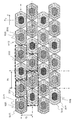
図4は、本開示の画素レイアウトの例を示す。図4は、画素(発光領域)のレイアウト、アノード電極162のレイアウト、及び有機発光層165の蒸着に使用する三つのFMMの開口のレイアウトの関係を示す。上述のように、R、G、及びBの色毎にFMMが用意され、FMMの開口を介した蒸着により、基板上に各色の有機発光層のパターンが形成される。図4は、三つのFMMの開口パターンを示す。なお、本開示の概念は、R、G、及びBの色群と異なる色群の画素に適用できる。
[Layout of pixels and FMM aperture]
FIG. 4 shows an example of the pixel layout of the present disclosure. FIG. 4 shows the relationship between the layout of the pixels (light emitting region), the layout of the
図4は、四つの画素行を、例として示す。各画素行は、図4においてX軸方向(第1方向)に配列された画素で構成されている。画素行を構成する画素が配列されている方向を行方向とも呼ぶ。複数の画素行は、行方向と垂直な方向である列方向(第2方向)に、配列されている。図4において、Y軸方向が列方向である。 FIG. 4 shows four pixel rows as an example. Each pixel row is composed of pixels arranged in the X-axis direction (first direction) in FIG. The direction in which the pixels constituting the pixel row are arranged is also called the row direction. The plurality of pixel rows are arranged in the column direction (second direction), which is the direction perpendicular to the row direction. In FIG. 4, the Y-axis direction is the column direction.
各画素行は、複数のR画素251R、複数のG画素251G、及び複数のB画素251Bで構成されている。図4においては、一つのR画素251R、一つのG画素251G、及び一つのB画素251が、例として符号で示されている。
Each pixel row is composed of a plurality of
各画素行において、3色の画素が、一定間隔(ピッチ)Pxで、循環的に配列されている。図4の例において、画素行を構成する画素は、R画素251R、G画素251G、及びB画素251B順で、循環的に配列されている。循環的配列において、同一色の画素の両隣の画素の色は、共通であり、同一色の隣接画素の間隔は一定の3Pxである。同一色の隣接画素の間隔は、3色の画素の間で共通である。色順序は全ての画素行の共通である。
In each pixel row, pixels of three colors are cyclically arranged at regular intervals (pitch) Px. In the example of FIG. 4, the pixels constituting the pixel row are sequentially arranged in the order of
図4の例において、R画素251R、G画素251G、及びB画素251Bは、同一の形状を有する。具体的には、各画素は、行方向に平行な2辺を含む、重心位置を通る任意の線において対称な八角形を有する。画素行を構成する画素の重心位置は、行方向に延びる直線上に位置する。画素行のおける画素の間隔Pxは、隣接する画素の重心間の距離である。
In the example of FIG. 4, the
複数の画素行は、列方向において、一定間隔(ピッチ)Pyで配列されている。間隔Pyは、隣接画素行それぞれの画素の重心を通る線の間の距離である。画素レイアウトは、千鳥配列である。奇数画素行の行方向における画素の位置及び色は、同一である。同様に、偶数画素行の行方向における画素の位置及び色は、同一である。 The plurality of pixel rows are arranged at regular intervals (pitch) Py in the column direction. The interval Py is the distance between the lines passing through the center of gravity of each pixel in the adjacent pixel row. The pixel layout is a staggered array. The positions and colors of the pixels in the row direction of the odd-numbered pixel rows are the same. Similarly, the positions and colors of pixels in the row direction of even pixel rows are the same.
各画素行は、隣接画素行に対して、(3/2)Pxだけずれている。画素は、行方向において、隣接画素行それぞれの、当該画素と同一色の隣接画素間の中央に位置する。具体的には、画素の重心は、隣接画素行それぞれの、当該画素と同一色の隣接画素の重心間の中央に位置する。 Each pixel row is offset by (3/2) Px with respect to the adjacent pixel row. The pixel is located in the row direction at the center of each adjacent pixel row between adjacent pixels of the same color as the pixel. Specifically, the center of gravity of a pixel is located at the center between the centers of gravity of adjacent pixels of the same color as the pixel in each adjacent pixel row.
例えば、一つのR画素251Rは、隣接画素行において隣接する二つのR画素251Rの間の中央に位置する。同様に、一つのG画素251G又はB画素251Bは、隣接画素行において隣接する二つのG画素251G又はB画素251Bの間の中央に位置する。
For example, one
図4は、リアル解像度の画素レイアウトを示す。表示画像の画素(表示画素又は主画素とも呼ぶ)は、隣接するR画素251R、G画素251G、及びB画素251で構成される。図4において、二つの表示画素255A、255Bが、例として符号で示されている。
FIG. 4 shows a pixel layout with real resolution. The pixels of the display image (also referred to as display pixels or main pixels) are composed of
表示画素255Aは、デルタ形状(三角形)を有する。具体的には、表示画素255Aは、k行(kは自然数)のG画素251G並びにk+1行のR画素251R及びB画素251Bで構成されている。表示画素255Bは、ナブラ形状(逆三角形)を有する。具体的には、表示画素255Bは、k行(kは自然数)のR画素251R及びB画素251B並びにk+1行のG画素251Gで構成されている。図4は、表示画素のいわゆるデルタナブラ配列を示す。デルタナブラ配列はデルタ形状の表示画素255Aとナブラ形状の表示画素255Bとを交互に配列する構成を有する。
The
画素のアノード電極162は、当該画素(画素定義層の開口167)よりも大きく、当該画素と相似形状(相似外形)を有する。具体的には、R画素251Rのアノード電極162Rは、当該R画素251Rよりも大きく、当該R画素251Rと相似な八角形を有する。同様に、G画素251G又はB画素251Bのアノード電極162G又は162Bは、当該G画素251G又はB画素251Bよりも大きく、当該G画素251G又はB画素251Bと相似な八角形を有する。画素と対応するアノード電極との間の比は、全画素に対して共通である。
The
画素と対応するアノード電極の重心位置は積層方向において見て一致している。つまり、R画素251R、G画素251G又はB画素251Bの重心位置と、アノード電極162R、162G又は162Bの重心位置とは、積層方向において見て一致している。画素とアノード電極との関係についての上記説明から理解されるように、画素と画素及び画素行についての上記説明は、アノード電極及びアノード電極の行に対して適用できる。
The positions of the centers of gravity of the anode electrodes corresponding to the pixels are the same when viewed in the stacking direction. That is, the position of the center of gravity of the
画素の有機発光材料を付着するためのFMMの開口は、当該画素(画素定義層の開口167)及びアノード電極よりも大きく、当該画素と相似形状(相似外形)を有する。具体的には、R画素251RのFMM開口541Rは、当該R画素251R及びアノード電極162Rよりも大きく、当該R画素251Rと相似な八角形を有する。
The opening of the FMM for adhering the organic light emitting material of the pixel is larger than the pixel (opening 167 of the pixel definition layer) and the anode electrode, and has a similar shape (similar outer shape) to the pixel. Specifically, the FMM opening 541R of the
同様に、G画素251GのFMM開口541Gは、当該G画素251G及びそのアノード電極162Gよりも大きく、当該G画素251Gと相似な八角形を有する。さらに、B画素251BのFMM開口541Bは、当該B画素251B及びそのアノード電極162Bよりも大きく、当該B画素251Bと相似な八角形を有する。画素と対応するFMM開口との間の比は、全画素に対して共通である。
Similarly, the
図4は、画素の重心位置と、画素に対応するFMM開口の重心位置とが積層方向において見て一致するように配置した、画素レイアウトとFMM開口レイアウトとを示す。図4は、R画素用FMM、G画素用FMM、及びB画素用FMMの三つのFMMの開口レイアウトを示す。R画素251R、G画素251G又はB画素251Bの重心位置と、FMM開口541R、541G又は541Bの重心位置とは、積層方向において見て一致している。
FIG. 4 shows a pixel layout and an FMM opening layout in which the position of the center of gravity of the pixel and the position of the center of gravity of the FMM opening corresponding to the pixel are arranged so as to coincide with each other in the stacking direction. FIG. 4 shows an aperture layout of three FMMs, an FMM for R pixels, an FMM for G pixels, and an FMM for B pixels. The position of the center of gravity of the
画素とFMM開口との関係についての上記説明から理解されるように、画素及び画素行についての上記説明は、FMM開口及びFMM開口の行に対して適用できる。各FMM、例えば、RのFMMに、複数のFMM開口541Rが形成されており、複数のFMM開口541Rは、複数の行を構成する。FMM開口541の行方向は、X軸方向である。
As understood from the above description of the relationship between pixels and FMM apertures, the above description of pixels and pixel rows is applicable to FMM apertures and rows of FMM apertures. A plurality of
FMM開口541Rの各行は、一定の間隔で配列されたFMM開口541Rで構成されている。FMM開口541Rの間隔は、行において隣接するFMM開口541Rの重心間の距離であり、3Pxである。各FMM開口541Rは、重心位置を通る任意の線において対称な八角形を有し、全てのFMM開口541Rが同一形状を有する。行を構成するFMM開口541Rの重心位置は、X軸方向に延びる線上に位置する。
Each row of the FMM opening 541R is composed of
各FMM、例えば、RのFMMにおいて、FMM開口541Rの行は、一定間隔Pyで列方向(Y軸方向)に配列されている。つまり、FMM開口541Rの行それぞれのFMM開口重心位置を通過する線の間の距離は、一定のPyである。FMM開口541Rのレイアウトは、千鳥配列である。 In each FMM, for example, the FMM of R, the rows of the FMM opening 541R are arranged in the column direction (Y-axis direction) at regular intervals Py. That is, the distance between the lines passing through the FMM opening center of gravity position of each row of the FMM opening 541R is a constant Py. The layout of the FMM opening 541R is a staggered arrangement.
各行は、隣接行に対して、(3/2)Pxだけずれている。FMM開口541Rは、行方向において、隣接行それぞれの、隣接FMM開口541R間の中央に位置する。具体的には、FMM開口541Rの重心は、隣接行それぞれの、隣接するFMM開口541Rの重心間の中央に位置する。
Each row is offset by (3/2) Px with respect to the adjacent row. The FMM opening 541R is located in the center of each adjacent row between
なお、FMM開口は、当該画素のアノード電極よりも小さくてもよい。実際の製造において、有機発光材料の蒸着のために基板151に対して位置決めされたFMM開口の重心位置は、画素の重心位置と必ずしも一致しない。画素とFMM開口との間の比は、製造プロセスで要求されるマージンにより規定される。
The FMM opening may be smaller than the anode electrode of the pixel. In actual production, the position of the center of gravity of the FMM opening positioned with respect to the
図5は、リアル解像度のデルタナブラ配列の画素の色パターンを示す。デルタ表示画素255Aは、三角形(デルタ形状)を形成し、G画素251Gを中心とする、R画素251R、G画素251G及びB画素251Bで構成される。ナブラ表示画素255Bは、逆三角形(ナブラ形状)を形成し、G画素251Gを中心とする、R画素251R、G画素251G及びB画素251Bで構成される。
FIG. 5 shows a color pattern of pixels in a real resolution delta nabla array. The
行方向の表示画素ピッチDPxと、列方向の表示画素ピッチDPyとは、同一である。したがって、破線の正方形257が示すように、R、G、及びBの色バランスは、正方形で取れる。 The display pixel pitch DPx in the row direction and the display pixel pitch DPy in the column direction are the same. Therefore, as indicated by the dashed square 257, the color balance of R, G, and B can be taken as a square.
図6は、図4に示す八角形画素の画素レイアウトにおける、行方向表示画素ピッチDPx、列方向表示画素ピッチDPy、行方向画素ピッチPx、及び列方向画素ピッチPyの関係を示す。行方向画素ピッチPxは、行方向表示画素ピッチDPxの2/3である。 Figure 6 shows the pixel layout of the octagon pixel shown in FIG. 4, the row direction display pixel pitch DPx, column Direction Table示画containing pitch DPy, row-direction pixel pitch Px, and the relationship between the column direction pixel pitch Py. The row direction pixel pitch Px is 2/3 of the row direction display pixel pitch DPx.
列方向画素ピッチPyは、列方向表示画素ピッチDPy(DPx)の1/2である。行方向画素ピッチPxと列方向画素ピッチPyの比は、(4/3)対1である。図6の例において、FMM開口の行方向の長さWxは、行方向画素ピッチPxと一致している。また、FMM開口の列方向の長さWyは、列方向画素ピッチPyと一致している。行方向に隣接する画素の重心間の中央及び列方向において隣接する画素の重心間の中央は、FMM開口の外周上に位置する。 The column direction pixel pitch Py is ½ of the column direction display pixel pitch DPy (DPx). The ratio of the row-direction pixel pitch Px to the column-direction pixel pitch Py is (4/3) to 1. In the example of FIG. 6, the row-direction length Wx of the FMM opening coincides with the row-direction pixel pitch Px. Further, the length Wy of the FMM opening in the row direction coincides with the pixel pitch Py in the row direction. The center between the centers of gravity of the pixels adjacent in the row direction and the center between the centers of gravity of the pixels adjacent in the column direction are located on the outer circumference of the FMM opening.
図7は、赤、緑、又は青の任意色の、画素、アノード電極、及び、FMM開口のレイアウトを示す。以下の説明は、赤、緑、及びBの全ての色の画素パターンに適用される。図7は、4組の画素、アノード電極、及び、FMM開口を例として示す。画素251Kは、画素251Jの隣接画素行において、画素251Jに隣接する同色画素である。画素251Kは、画素251Jの隣接画素行に含まれ、当該隣接画素行において画素251Jに最も近い同色画素である。
FIG. 7 shows the layout of pixels, anode electrodes, and FMM apertures of any color, red, green, or blue. The following description applies to pixel patterns of all colors red, green, and B. FIG. 7 shows four sets of pixels, an anode electrode, and an FMM aperture as an example. The
画素251Jと隣接する画素行に含まれ、画素251Jに隣接する四つの同色画素が存在する。四つの同色画素の一つが画素251Kであり、以下に説明する画素251Jと画素251Kとの関係は、他の三つの同色画素と画素251Jとの関係にも適用される。
There are four pixels of the same color included in the pixel row adjacent to the
画素251Jと画素251Kとの距離は、これらの重心間の距離である。画素251Jは、画素251Kに対向する辺611Jを含む。画素251Kは、画素251Jに対向する辺611Kを含む。画素251J、251Kの互いに対向する辺611J、611Kは、画素251Jの重心と画素251Kの重心とを結ぶ線(重心結合線)と交差する。
The distance between the
画素251Jの外周と、画素251Kの外周との間の距離は、互いに対向する辺611J、611Kの間の距離である。図7において、対向する辺611J、611K間の距離はB1で表わされる。図7は、説明のため、画素251Lと画素251Mとの間において距離B1を示す。画素251Lと画素251Mとの関係は、画素251Jと画素251Kとの間の関係と同様である。
The distance between the outer circumference of the
画素251Jの重心と画素251Kの重心とを結ぶ線(重心結合線)は、対向する辺611J、611Kそれぞれと垂直(90.0度)である。したがって、重心結合線と辺611J、611Kそれぞれとが交差する点の距離が、辺611J、611K間の距離B1である。
The line connecting the center of gravity of the
画素251Jの重心と画素251Kの重心との行方向(X軸方向)における距離は、1.5Pxである。画素251Jの重心と画素251Kの重心との列方向(Y軸方向)における距離は、Pyである。上述のように、リアル解像度において、PxとPyの比は、4対3である。辺611Jと画素251Jの重心と画素251Kの重心とを結ぶ線(重心結合線)との間の角度は90.0度である。したがって、辺611Kと行方向(X軸方向)とがなす角度θ1は、63.4度である。辺611Jと行方向(X軸方向)とがなす角度も、θ1=63.4度である。
The distance between the center of gravity of the
同様の説明が、アノード電極162J、162K及びFMM開口541J、541Kに適用できる。FMM開口541J、541Kについて具体的に説明する。FMM開口541Kは、FMM開口541Jの隣接行において、FMM開口541Jに隣接するFMM開口である。FMM開口541Kは、FMM開口541Jの隣接行に含まれ、当該隣接行においてFMM開口541Jに最も近いFMM開口である。
Similar description can be applied to
FMM開口541Jと隣接する行に含まれ、FMM開口541Jに隣接する四つのFMM開口が存在する。四つのFMM開口の一つがFMM開口541Kであり、以下に説明するFMM開口541JとFMM開口541Kとの関係は、他の三つのFMM開口とFMM開口541Jとの関係にも適用される。
There are four FMM openings included in the row adjacent to the FMM opening 541J and adjacent to the
FMM開口541JとFMM開口541Kとの距離は、これらの重心間の距離である。FMM開口541Jは、FMM開口541Kに対向する辺613Jを含む。FMM開口541Kは、FMM開口541Jに対向する辺613Kを含む。FMM開口541J、541Kの互いに対向する辺613J、613Kは、FMM開口541Jの重心とFMM開口541Kの重心とを結ぶ線(重心結合線)と交差する。
The distance between the FMM opening 541J and the
FMM開口541Jの外周と、FMM開口541Kの外周との間の距離は、互いに対向する辺613J、613Kの間の距離である。図7において、対向する辺613J、613K間の距離はB2で表わされる。図7は、説明のため、FMM開口541LとFMM開口541Mとの間において距離B2を示す。FMM開口541LとFMM開口541Mとの関係は、FMM開口541JとFMM開口541Kとの間の関係と同様である。
The distance between the outer circumference of the FMM opening 541J and the outer circumference of the
FMM開口541Jの重心とFMM開口541Kの重心とを結ぶ線(重心結合線)は、対向する辺613J、613Kそれぞれと垂直(90.0度)である。したがって、重心結合線と辺613J、613Kそれぞれとが交差する点の距離が、辺613J、613K間の距離B2である。
The line connecting the center of gravity of the FMM opening 541J and the center of gravity of the
FMM開口541Jの重心とFMM開口541Kの重心との行方向(X軸方向)における距離は、1.5Pxである。FMM開口541Jの重心とFMM開口541Kの重心との列方向(Y軸方向)における距離は、Pyである。辺613JとFMM開口541Jの重心とFMM開口541Kの重心とを結ぶ線(重心結合線)との間の角度は90.0度である。したがって、辺613Kと行方向(X軸方向)とがなす角度θ2は、63.4度である。辺613Jと行方向(X軸方向)とがなす角度も、θ2=63.4度である。
The distance between the center of gravity of the FMM opening 541J and the center of gravity of the
次に、画素251Jと画素251Lとの関係を説明する。画素251Lは、列方向において画素251Jと隣接する同色画素である。画素251Lは、画素251Jが含まれる画素行の二つ隣の画素行において、画素251Jに最も近い同色画素である。画素251Jと列方向において隣接する二つの同色画素が存在する。二つの同色画素の一つが画素251Lであり、以下に説明する画素251Jと画素251Lとの関係は、他の一つの画素と画素251Jとの関係にも適用される。
Next, the relationship between the
画素251Jと画素251Lとの距離は、これらの重心間の距離である。画素251Jは、画素251Lに対向する辺615Jを含む。画素251Lは、画素251Jに対向する辺615Lを含む。画素251J、251Lの互いに対向する辺615J、615Lは、画素251Jの重心と画素251Lの重心とを結ぶ線(重心結合線)と交差する。辺615J、615Lは、行方向(X軸方向)に平行である。
The distance between the
画素251Jの外周と、画素251Lの外周との間の距離は、互いに対向する辺615J、615Lの間の距離である。図7において、対向する辺615J、615L間の距離はC1で表わされる。画素251Jの重心と画素251Kの重心とを結ぶ線(重心結合線)は、列方向(Y軸方向)に平行である。したがって、重心結合線は、対向する辺615J、615Lそれぞれと垂直(90.0度)である。重心結合線と辺615J、615Lそれぞれとが交差する点の距離が、辺615J、615L間の距離C1である。
The distance between the outer circumference of the
同様の説明が、アノード電極162J、162L及びFMM開口541J、541Lに適用できる。FMM開口541J、541Lについて具体的に説明する。FMM開口541Lは、列方向においてFMM開口541Jと隣接するFMM開口である。FMM開口541Lは、FMM開口541Jが含まれる行の二つ隣の行において、FMM開口541Jに最も近いFMM開口である。FMM開口541Jと列方向において隣接する二つのFMM開口が存在する。二つのFMM開口の一つがFMM開口541Lであり、以下に説明するFMM開口541JとFMM開口541Lとの関係は、他の一つのFMM開口とFMM開口541Jとの関係にも適用される。
The same description can be applied to the
FMM開口541JとFMM開口541Lとの距離は、これらの重心間の距離である。FMM開口541Jは、FMM開口541Lに対向する辺617Jを含む。FMM開口541Lは、FMM開口541Jに対向する辺617Lを含む。FMM開口541J、541Lの互いに対向する辺617J、617Lは、FMM開口541Jの重心とFMM開口541Lの重心とを結ぶ線(重心結合線)と交差する。辺617J、617Lは、行方向(X軸方向)に平行である。
The distance between the FMM opening 541J and the
FMM開口541Jの外周と、FMM開口541Lの外周との間の距離は、互いに対向する辺617J、617Lの間の距離である。図7において、対向する辺617J、617L間の距離はC2で表わされる。FMM開口541Jの重心とFMM開口541Lの重心とを結ぶ線(重心結合線)は、列方向(Y軸方向)に平行である。したがって、重心結合線は、対向する辺617J、617Lそれぞれと垂直(90.0度)である。重心結合線と辺617J、617Lそれぞれとが交差する点の距離が、辺617J、617L間の距離C2である。
The distance between the outer circumference of the FMM opening 541J and the outer circumference of the
人の目の特性として、多角形(円を含む)で発光する3原色の画素が近い距離で隣接している場合、隣接する画素の3原色を混色させた一つのフルカラー画素を認識する。3色の画素の理想的な混色(画素が目立たない自然な画像の実現)を行うためには、同色の画素(発光領域)の分布が、それぞれの重心に対して対称であり、かつ、画素面積が大きいことが好ましい。したがって、画素形状は、重心を通過する任意の線について対称であり、かつ、重心から画素端までの距離が大きいことが重要である。 As a characteristic of the human eye, when pixels of three primary colors emitting light in a polygon (including a circle) are adjacent to each other at a short distance, one full-color pixel in which the three primary colors of adjacent pixels are mixed is recognized. In order to achieve ideal color mixing of three color pixels (realization of a natural image in which the pixels are inconspicuous), the distribution of pixels of the same color (light emitting area) is symmetrical with respect to the center of gravity of each, and the pixels. Larger area is preferred. Therefore, it is important that the pixel shape is symmetrical with respect to any line passing through the center of gravity and that the distance from the center of gravity to the pixel end is large.
一方、FMMを使用した有機発光材料の高精度の蒸着のためには、蒸着時のFMMの変形を小さくすることが必要である。FMMの変形を小さくするためには、FMMのブリッジ幅を大きくすることが重要である。ブリッジ幅は、隣接FMM開口の外周間の距離である。図7に示す例において、距離B2は、斜め方向におけるブリッジ幅であり、距離C2は列方向(Y軸方向)におけるブリッジ幅である。斜め方向は、行方向(X軸方向)と列方向(Y軸方向)との間の方向である。 On the other hand, for high-precision thin-film deposition of organic light-emitting materials using FMM, it is necessary to reduce the deformation of FMM during vapor deposition. In order to reduce the deformation of the FMM, it is important to increase the bridge width of the FMM. The bridge width is the distance between the outer circumferences of adjacent FMM openings. In the example shown in FIG. 7, the distance B2 is the bridge width in the diagonal direction, and the distance C2 is the bridge width in the column direction (Y-axis direction). The diagonal direction is the direction between the row direction (X-axis direction) and the column direction (Y-axis direction).
隣接する同色画素の対向辺が隣接する同色画素の重心を結ぶ線の垂線であり、また、隣接するFMM開口の対向辺がFMM開口の重心を結ぶ線の垂線である場合、所望のブリッジ幅を確保しながら、画素の重心から画素端(外周)までの距離を最大化することができる。 When the opposite side of the adjacent same-color pixel is a perpendicular line connecting the center of gravity of the adjacent same-color pixel, and the opposite side of the adjacent FMM opening is a perpendicular line of the line connecting the center of gravity of the FMM opening, the desired bridge width is obtained. While ensuring, the distance from the center of gravity of the pixel to the edge of the pixel (outer circumference) can be maximized.
図7に示すように、デルタナブラ配列の画素レイアウトにおいて、各画素に隣接する同色画素のうち、距離が近い画素は、列方向の二つの画素及び斜め方向の四つの画素である。図7の例において、画素251Lは画素251Jの列方向において隣接する画素であり、画素251K、251Mは、画素251Jの斜め方向において隣接する画素である。行方向において隣接する画素間の距離は、列方向における画素間距離及び斜め方向における画素間距離よりも大きい。
As shown in FIG. 7, in the pixel layout of the delta nabla arrangement, among the pixels of the same color adjacent to each pixel, the pixels having a short distance are two pixels in the column direction and four pixels in the diagonal direction. In the example of FIG. 7, the
したがって、図7に示す画素配列において、上記条件を満たし、画素面積を大きくするためには、画素形状は、六角形又は八角形であって、その列方向及び斜め方向に隣接する同色画素と対向する辺が、それぞれ、隣接同色画素の重心結合線に垂直である。図7に示す八角形の画素形状は、この条件を満たす。上記条件を満たす六角形は、重心を通過する行方向に延びる線上に二つの角を有する。 Therefore, in the pixel arrangement shown in FIG. 7, in order to satisfy the above conditions and increase the pixel area, the pixel shape is hexagonal or octagonal, and faces the pixels of the same color adjacent to each other in the column direction and the diagonal direction. Each side is perpendicular to the center of gravity coupling line of adjacent pixels of the same color. The octagonal pixel shape shown in FIG. 7 satisfies this condition. A hexagon satisfying the above conditions has two angles on a line extending in the row direction passing through the center of gravity.
同様に、上記条件を満たすFMM開口の形状は六角形又は八角形であって、列方向及び斜め方向に隣接するFMM開口と対向する辺が、それぞれ、隣接FMM開口の重心結合線に垂直である。図7に示す八角形の開口形状は、この条件を満たす。上記条件を満たす六角形は、重心を通過する行方向に延びる線上に二つの角を有する。 Similarly, the shape of the FMM opening satisfying the above conditions is hexagonal or octagonal, and the sides facing the adjacent FMM openings in the column direction and the diagonal direction are perpendicular to the center of gravity coupling line of the adjacent FMM openings, respectively. .. The octagonal opening shape shown in FIG. 7 satisfies this condition. A hexagon satisfying the above conditions has two angles on a line extending in the row direction passing through the center of gravity.
上述のように、図7を参照して説明した画素形状及び画素レイアウト、並びに、FMM開口形状及びFMM開口レイアウトは、重心に対して対称であり大きな面積の画素形状と、より広いブリッジ幅とを実現することができる。 As described above, the pixel shape and pixel layout described with reference to FIG. 7, and the FMM aperture shape and FMM aperture layout are symmetrical with respect to the center of gravity and have a large area pixel shape and a wider bridge width. It can be realized.
図8は、画素又はFMM開口の形状の例を示す。形状801は、曲線コーナの八角形を示す。形状803は、曲線コーナの六角形を示す。画素又はFMM開口の形状は、これらのように、曲線コーナの六角形又は八角形でもよい。同様の説明が、アノード電極162の形状に適用できる。
FIG. 8 shows an example of the shape of a pixel or FMM opening.
[画素制御]
図9は、図4と同一の画素レイアウトにおける、画素(アノード電極)及び配線のレイアウト並びに画素(アノード電極)と配線との接続関係の例を模式的に示す。図9は、一例を示すものであって、他の任意の接続関係を上記画素レイアウトに適用することができる。
[Pixel control]
FIG. 9 schematically shows an example of the layout of pixels (anode electrodes) and wiring and the connection relationship between pixels (anode electrodes) and wiring in the same pixel layout as in FIG. FIG. 9 shows an example, and any other connection relationship can be applied to the pixel layout.
図9は、12の画素、3本のデータ線Xam、Xbm、Xcm、4本の走査線Yn、Yn+1、Yn+2、Yn+3、及び、3本の電力供給線811を示す。表示領域125における他の領域も、図9と同様の構成を有する。
FIG. 9 shows 12 pixels, 3 data lines Xam, Xbm, Xcm, 4 scanning lines Yn, Yn + 1, Yn + 2, Yn + 3, and 3
走査線Yn、Yn+1、Yn+2、Yn+3は、それぞれ、n番目、n+1番目、n+2番目、n+3番目の画素行に接続されている。走査線Yn、Yn+1、Yn+2、Yn+3は、順次、接続されている画素行に走査信号を供給する。走査線から供給される走査信号により、接続されている画素行の全画素が選択される。 The scanning lines Yn, Yn + 1, Yn + 2, and Yn + 3 are connected to the nth, n + 1th, n + 2nd, and n + 3rd pixel rows, respectively. The scanning lines Yn, Yn + 1, Yn + 2, and Yn + 3 sequentially supply scanning signals to the connected pixel rows. The scan signal supplied from the scan line selects all the pixels in the connected pixel row.
データ線Xamは、R画素とG画素が交互に配列されている画素列に接続されている。データ線Xbmは、G画素とB画素が交互に配列されている画素列に接続されている。データ線Xcmは、B画素とR画素が交互に配列されている画素列に接続されている。データ線Xamは、R画素への出力及びG画素への出力を交互に繰り返す。データ線Xbmは、G画素への出力及びB画素への出力を交互に繰り返す。データ線Xcmは、B画素への出力及びR画素への出力を交互に繰り返す。 The data line Xam is connected to a pixel array in which R pixels and G pixels are alternately arranged. The data line Xbm is connected to a pixel array in which G pixels and B pixels are alternately arranged. The data line Xcm is connected to a pixel array in which B pixels and R pixels are alternately arranged. The data line Xam alternately repeats the output to the R pixel and the output to the G pixel. The data line Xbm alternately repeats the output to the G pixel and the output to the B pixel. The data line Xcm alternately repeats the output to the B pixel and the output to the R pixel.
データ線Xam、Xbm、Xcmと電力供給線811とは、交互に配置されている。図9の例において、各電力供給線811は、隣接する1本のデータ線(例えば左側のデータ線)に接続される駆動トランジスタを介して電力を画素に供給する。表示領域125における他の領域において、データ線Xam、Xbm、Xcmと画素との接続関係と同様の接続関係が繰り返される。
The data lines Xam, Xbm, Xcm and the
図10は、図9に示す画素レイアウトにおける、画素の駆動のタイミングチャートを示す。図10は、データ線Xam、データ線Xbm及びデータ線Xcmからのデータ信号(以下、信号と記す)の波形、並びに、走査線Yn、Yn+1、Yn+2及びYn+3からの選択パルスの波形を示す。走査線Yn、Yn+1、Yn+2及びYn+3は、異なるタイミングで、順次選択パルスを出力する。なお、走査ドライバ回路131が、走査線Yn、Yn+1、Yn+2及びYn+3に選択パルスを出力する。また、ドライバIC134が、データ線Xam、データ線Xbm及びデータ線Xcmにデータ信号を出力する。
FIG. 10 shows a timing chart of pixel drive in the pixel layout shown in FIG. FIG. 10 shows waveforms of data signals (hereinafter referred to as signals) from data lines Xam, data lines Xbm and data lines Xcm, and waveforms of selection pulses from scanning lines Yn, Yn + 1, Yn + 2 and Yn + 3. The scanning lines Yn, Yn + 1, Yn + 2 and Yn + 3 sequentially output selection pulses at different timings. The
走査線Ynが選択パルスを出力している間、データ線Xamは、n番目の画素行のR画素に信号を出力する。走査線Ynが選択パルスを出力している間、データ線Xbmは、n番目の画素行のG画素に信号を出力する。走査線Ynが選択パルスを出力している間、データ線Xcmは、n番目の画素行のB画素に信号を出力する。 While the scanning line Yn outputs the selection pulse, the data line Xam outputs a signal to the R pixel of the nth pixel row. While the scanning line Yn outputs the selection pulse, the data line Xbm outputs a signal to the G pixel of the nth pixel row. While the scanning line Yn outputs the selection pulse, the data line Xcm outputs a signal to the B pixel of the nth pixel row.
走査線Yn+1が選択パルスを出力している間、データ線Xamは、n+1番目の画素行のG画素に信号を出力する。走査線Yn+1が選択パルスを出力している間、データ線Xbmは、n+1番目の画素行のB画素に信号を出力する。走査線Yn+1が選択パルスを出力している間、データ線Xcmは、n+1番目の画素行のR画素に信号を出力する。 While the scan line Yn + 1 outputs the selection pulse, the data line Xam outputs a signal to the G pixel of the n + 1th pixel row. While the scan line Yn + 1 outputs the selection pulse, the data line Xbm outputs a signal to the B pixel of the n + 1th pixel row. While the scan line Yn + 1 outputs the selection pulse, the data line Xcm outputs a signal to the R pixel of the n + 1th pixel row.
走査線Yn+2が選択パルスを出力している間、データ線Xamは、n+2番目の画素行のR画素に信号を出力する。走査線Yn+2が選択パルスを出力している間、データ線Xbmは、n+2番目の画素行のG画素に信号を出力する。走査線Yn+2が選択パルスを出力している間、データ線Xcmは、n+2番目の画素行のB画素に信号を出力する。 While the scan line Yn + 2 outputs the selection pulse, the data line Xam outputs a signal to the R pixel of the n + second pixel row. While the scan line Yn + 2 outputs the selection pulse, the data line Xbm outputs a signal to the G pixel of the n + second pixel row. While the scanning line Yn + 2 outputs the selection pulse, the data line Xcm outputs a signal to the B pixel of the n + second pixel row.
走査線Yn+3が選択パルスを出力している間、データ線Xamは、n+3番目の画素行のG画素に信号を出力する。走査線Yn+3が選択パルスを出力している間、データ線Xbmは、n+3番目の画素行のB画素に信号を出力する。走査線Yn+3が選択パルスを出力している間、データ線Xcmは、n+3番目の画素行のR画素に信号を出力する。 While the scan line Yn + 3 outputs the selection pulse, the data line Xam outputs a signal to the G pixel of the n + 3rd pixel row. While the scanning line Yn + 3 outputs the selection pulse, the data line Xbm outputs a signal to the B pixel of the n + 3rd pixel row. While the scanning line Yn + 3 outputs the selection pulse, the data line Xcm outputs a signal to the R pixel of the n + 3rd pixel row.
走査線Yn及びYn+1は、1水平期間(1H)において、順次選択パルスを出力する。走査線Yn+2及びYn+3は、次の1水平期間(1H)において、順次選択パルスを出力する。選択パルス幅は共通であり、走査線Yn、Yn+1、Yn+2及びYn+3は、それぞれ、略1/2水平期間の間、選択パルスを出力する。 The scanning lines Yn and Yn + 1 output sequential selection pulses in one horizontal period (1H). The scanning lines Yn + 2 and Yn + 3 sequentially output selection pulses in the next one horizontal period (1H). The selection pulse width is common, and the scan lines Yn, Yn + 1, Yn + 2 and Yn + 3 each output a selection pulse for approximately 1/2 horizontal period.
[FMM開口レイアウト]
以下において、FMMにおける開口幅とブリッジ幅との関係を説明する。図11は、赤、緑、又は青の任意色のFMMのFMM開口レイアウトを示す。以下の説明は、赤、緑、及びBの全ての色のFMMに適用される。図7を参照した説明が、図11に対しても適用される。
[FMM opening layout]
In the following, the relationship between the opening width and the bridge width in the FMM will be described. FIG. 11 shows an FMM aperture layout of an FMM of any color, red, green, or blue. The following description applies to FMMs of all colors red, green, and B. The description with reference to FIG. 7 also applies to FIG.
FMM開口の列方向における幅は、2r1で表わされる。FMM開口の斜め方向における幅は、2r2で表わされる。斜め方向は、隣接行の隣接FMM開口間の重心を結ぶ方向である。 The width of the FMM opening in the row direction is represented by 2r1. The diagonal width of the FMM opening is represented by 2r2. The diagonal direction is the direction connecting the center of gravity between the adjacent FMM openings in the adjacent row.
FMMの変形を小さくするためには、ブリッジ幅B2が、FMM開口の最小幅A以上であることが好ましい。さらに、ブリッジ幅C2が、FMM開口の最小幅A以上であることが好ましい。図11の例において、FMM開口の最小幅Aは、2r1である。FMMは、本例の蒸着工程において、行方向に引っ張られた状態で、位置決めされる。引張方向成分を含むブリッジ幅B2とFMM開口の最小幅Aとの関係がより重要である。 In order to reduce the deformation of the FMM, it is preferable that the bridge width B2 is equal to or larger than the minimum width A of the FMM opening. Further, it is preferable that the bridge width C2 is equal to or larger than the minimum width A of the FMM opening. In the example of FIG. 11, the minimum width A of the FMM opening is 2r1. In the vapor deposition process of this example, the FMM is positioned while being pulled in the row direction. The relationship between the bridge width B2 including the tensile direction component and the minimum width A of the FMM opening is more important.
図11に示すFMM開口レイアウトにおいて、列方向のブリッジ幅C2は、(2Py−2r1)である。Pyは列方向におけるFMM開口ピッチ(画素ピッチ)である。斜め方向のブリッジ幅B2は、(Py√5−2r2)である。 In the FMM opening layout shown in FIG. 11, the bridge width C2 in the column direction is (2Py-2r1). Py is the FMM aperture pitch (pixel pitch) in the column direction. The bridge width B2 in the diagonal direction is (Py√5-2r2).
FMMの変形を抑制するために、以下の条件を満たすことが好ましい。
ブリッジ幅B2=(Py√5−2r2)≧FMM開口最小幅A=2r1
FMMの変形を抑制するために、さらに以下の条件を満たすことが好ましい。
ブリッジ幅C2=(2Py−2r1)≧FMM開口最小幅A=2r1
In order to suppress the deformation of FMM, it is preferable to satisfy the following conditions.
Bridge width B2 = (Py√5-2r2) ≧ FMM opening minimum width A = 2r1
In order to suppress the deformation of FMM, it is preferable to further satisfy the following conditions.
Bridge width C2 = (2Py-2r1) ≧ FMM opening minimum width A = 2r1
図12は、赤、緑、又は青の任意色のFMMのFMM開口レイアウトの他の例を示す。以下の説明は、赤、緑、及びBの全ての色のFMMに適用される。FMM開口は真円である。FMM開口の重心(真円の中心)の配列は、図11に示すレイアウトと同様である。 FIG. 12 shows another example of the FMM aperture layout of an FMM of any color, red, green, or blue. The following description applies to FMMs of all colors red, green, and B. The FMM opening is a perfect circle. The arrangement of the center of gravity (center of the perfect circle) of the FMM opening is the same as the layout shown in FIG.
真円のFMM開口の半径はrで表わされている。図11を参照して説明したように、FMMの変形を抑制するために、以下の条件を満たすことが好ましい。
ブリッジ幅B2=(Py√5−2r)≧FMM開口最小幅A=2r
FMMの変形を抑制するために、さらに以下の条件を満たすことが好ましい。
ブリッジ幅C2=(2Py−2r)≧FMM開口最小幅A=2r
The radius of the FMM opening of a perfect circle is represented by r. As described with reference to FIG. 11, it is preferable to satisfy the following conditions in order to suppress the deformation of the FMM.
Bridge width B2 = (Py√5-2r) ≧ FMM opening minimum width A = 2r
In order to suppress the deformation of FMM, it is preferable to further satisfy the following conditions.
Bridge width C2 = (2Py-2r) ≧ FMM opening minimum width A = 2r
上記説明は、同色画素のレイアウト及び同色画素のアノード電極のレイアウトにも適用できる。上述のように、同色画素の重心配列は、FMM開口の重心配列と同一であり、画素形状は、FMM開口形状より小さく、相似である。したがって、斜め方向に隣接する同色画素の外形間の距離B1又は列方向に隣接する同色画素の外形間の距離C1は、画素幅の最小値以上であることが好ましい。アノード電極について同様である。 The above description can be applied to the layout of the same color pixels and the layout of the anode electrodes of the same color pixels. As described above, the center-of-gravity array of the same-color pixels is the same as the center-of-gravity array of the FMM aperture, and the pixel shape is smaller and similar to the FMM aperture shape. Therefore, it is preferable that the distance B1 between the outer shapes of the same color pixels adjacent in the diagonal direction or the distance C1 between the outer shapes of the same color pixels adjacent in the column direction is equal to or larger than the minimum value of the pixel width. The same applies to the anode electrode.
[画素及びFMM開口の他のレイアウト]
図13は、レンダリングにより画像を表示するデルタナブラ配列の、画素レイアウトを示す。具体的には、デルタナブラ縦方向2/3画素レンダリングの画素レイアウトを示す。画素列(データ線)の数はリアル解像度と同様であり、画素行(走査線)の数はリアル解像度の2/3である。この構成はTFT回路の設計を容易にすることができる。この構成によれば、走査ドライバ131やエミッションドライバ132の出力数を減らすことができるので、TFT回路の設計が容易となりドライバの占有面積も縮小できる。
[Other layouts of pixels and FMM aperture]
FIG. 13 shows a pixel layout of a delta nabla array that displays an image by rendering. Specifically, the pixel layout of the delta nabla vertical 2/3 pixel rendering is shown. The number of pixel columns (data lines) is the same as the real resolution, and the number of pixel rows (scanning lines) is 2/3 of the real resolution. This configuration can facilitate the design of the TFT circuit. According to this configuration, the number of outputs of the
図4と同様に、図13は、画素、アノード電極及び三つのFMMのFMM開口のレイアウトを示す。以下において、図4〜6を参照して説明したリアル解像度デルタナブラ配列との相違点を、主に説明する。 Similar to FIG. 4, FIG. 13 shows the layout of the pixels, the anode electrodes and the FMM openings of the three FMMs. In the following, the differences from the real resolution delta nabla array described with reference to FIGS. 4 to 6 will be mainly described.
図4に示すリアル解像度のレイアウトと比較して、行方向の画素ピッチPxと列方向の画素ピッチPyとの比が異なる。さらに、画素、アノード電極及びFMM開口それぞれの縦横比が異なる。縦方向は列方向であり、横方向は行方向である。 Compared with the layout of the real resolution shown in FIG. 4, the ratio of the pixel pitch Px in the row direction to the pixel pitch Py in the column direction is different. Further, the aspect ratios of the pixels, the anode electrodes, and the FMM openings are different. The vertical direction is the column direction, and the horizontal direction is the row direction.
図14は、デルタナブラ縦方向2/3画素レンダリングの、画素の色パターンを示す。破線の長方形258が示すように、R、G、及びBの色バランスは、縦横比が3対2の長方形で取れる。レンダリングによる表示画素の定義は、リアル解像度の表示画素と異なり、あいまいである。
FIG. 14 shows a pixel color pattern of a delta nabla vertical 2/3 pixel rendering. As indicated by the dashed
行方向画素ピッチPxと列方向画素ピッチPyの比は、8対9である。リアル解像度と同様に、FMM開口の行方向の長さWxは、行方向画素ピッチPxと一致している。また、FMM開口の列方向の長さWyは、列方向画素ピッチPyと一致している。 The ratio of the row-direction pixel pitch Px to the column-direction pixel pitch Py is 8: 9. Similar to the real resolution, the row length Wx of the FMM aperture coincides with the row pixel pitch Px. Further, the length Wy of the FMM opening in the row direction coincides with the pixel pitch Py in the row direction.
図15は、デルタナブラ縦方向2/3画素レンダリングに対応する、赤、緑、又は青の任意色の、画素、アノード電極、及び、FMM開口のレイアウトを示す。以下の説明は、赤、緑、及びBの全ての色の画素パターンに適用される。以下においては、図7を参照して説明したリアル解像度のレイアウトとの相違点を主に説明する。 FIG. 15 shows a layout of pixels, anode electrodes, and FMM openings of any color, red, green, or blue, corresponding to Delta Nabla vertical 2/3 pixel rendering. The following description applies to pixel patterns of all colors red, green, and B. In the following, the differences from the real resolution layout described with reference to FIG. 7 will be mainly described.
リアル解像度と同様に、画素251Jの重心と画素251Kの重心とを結ぶ線(重心結合線)は、対向する辺611J、611Kそれぞれと垂直(90.0度)である。上述のように、行方向画素ピッチPxと列方向画素ピッチPyの比が、リアル解像度のレイアウトと異なり、行方向画素ピッチPxと列方向画素ピッチPyの比は、8対9である。したがって、辺611Kと行方向(X軸方向)とがなす角度θ1は、53.1度である。辺611Jと行方向(X軸方向)とがなす角度も、θ1=53.1度である。
Similar to the real resolution, the line connecting the center of gravity of the
リアル解像度と同様に、FMM開口541Jの重心とFMM開口541Kの重心とを結ぶ線(重心結合線)は、対向する辺613J、613Kそれぞれと垂直(90.0度)である。
Similar to the real resolution, the line connecting the center of gravity of the FMM opening 541J and the center of gravity of the
FMM開口541Jの重心とFMM開口541Kの重心との行方向(X軸方向)における距離は、1.5Pxである。FMM開口541Jの重心とFMM開口541Kの重心との列方向(Y軸方向)における距離は、Pyである。
The distance between the center of gravity of the FMM opening 541J and the center of gravity of the
さらに、辺613JとFMM開口541Jの重心とFMM開口541Kの重心とを結ぶ線(重心結合線)との間の角度は90.0度である。したがって、辺613Kと行方向(X軸方向)とがなす角度θ2は、53.1度である。辺613Jと行方向(X軸方向)とがなす角度も、θ2=53.1度である。
Further, the angle between the
図11又は図12を参照した説明を、デルタナブラ縦方向2/3画素レンダリングのFMM開口レイアウトにも適用することができる。デルタナブラ縦方向2/3画素レンダリングのFMM開口レイアウトにおいて、列方向のブリッジ幅C2は、(2Py−2r1)である。また、斜め方向のブリッジ幅B2は、(5Py/3−2r2)である。なお、図15に示すように、2つの画素の重心結合線を斜辺とする直角三角形において、底辺と短辺(高さ)と斜辺と比は4(図15では”2”と図示):3(図15では”1.5”と図示):5であり、この重心結合線に沿った方向における開口幅の半分がr2(図11参照)なので、斜め方向のブリッジ幅B2は、上記した式で示すことができる。 The description with reference to FIG. 11 or 12 can also be applied to the FMM aperture layout for delta nabla vertical 2/3 pixel rendering. In the FMM aperture layout of the delta nabla vertical 2/3 pixel rendering, the bridge width C2 in the column direction is (2Py-2r1). Further, the bridge width B2 in the diagonal direction is (5Py / 3-2r2). As shown in FIG. 15, in a right triangle whose hypotenuse is the center of gravity of two pixels, the ratio of the base, the short side (height), and the hypotenuse is 4 (shown as "2" in FIG. 15): 3. (Indicated as "1.5" in FIG. 15): 5, and half of the opening width in the direction along the center of gravity coupling line is r2 (see FIG. 11), so the bridge width B2 in the diagonal direction is shown by the above equation. be able to.
したがって、FMMの変形を抑制するために、六角形又は八角形のFMM開口のレイアウトは、以下の条件を満たすことが好ましい。
ブリッジ幅B2=(5Py/3−2r2)≧FMM開口最小幅A=2r1
FMMの変形を抑制するために、さらに以下の条件を満たすことが好ましい。
ブリッジ幅C2=(2Py−2r1)≧FMM開口最小幅A=2r1
Therefore, in order to suppress the deformation of the FMM, it is preferable that the layout of the hexagonal or octagonal FMM opening satisfies the following conditions.
Bridge width B2 = (5Py / 3-2r2) ≧ FMM opening minimum width A = 2r1
In order to suppress the deformation of FMM, it is preferable to further satisfy the following conditions.
Bridge width C2 = (2Py-2r1) ≧ FMM opening minimum width A = 2r1
また、真円のFMM開口のレイアウトは、以下の条件を満たすことが好ましい。
ブリッジ幅B2=(5Py/3−2r)≧FMM開口最小幅A=2r
FMMの変形を抑制するために、さらに以下の条件を満たすことが好ましい。
ブリッジ幅C2=(2Py−2r)≧FMM開口最小幅A=2r
Further, it is preferable that the layout of the FMM opening of a perfect circle satisfies the following conditions.
Bridge width B2 = (5Py / 3-2r) ≧ FMM opening minimum width A = 2r
In order to suppress the deformation of FMM, it is preferable to further satisfy the following conditions.
Bridge width C2 = (2Py-2r) ≧ FMM opening minimum width A = 2r
上記説明は、同色画素のレイアウト及び同色画素のアノード電極のレイアウトにも適用できる。上述のように、同色画素の重心配列は、FMM開口の重心配列と同一であり、画素形状は、FMM開口形状より小さく、相似である。したがって、斜め方向に隣接する同色画素の外形間の距離B1又は列方向に隣接する同色画素の外形間の距離C1は、画素幅の最小値以上であることが好ましい。アノード電極について同様である。 The above description can be applied to the layout of the same color pixels and the layout of the anode electrodes of the same color pixels. As described above, the center-of-gravity array of the same-color pixels is the same as the center-of-gravity array of the FMM aperture, and the pixel shape is smaller and similar to the FMM aperture shape. Therefore, it is preferable that the distance B1 between the outer shapes of the same color pixels adjacent in the diagonal direction or the distance C1 between the outer shapes of the same color pixels adjacent in the column direction is equal to or larger than the minimum value of the pixel width. The same applies to the anode electrode.
[画素及びFMM開口の他のレイアウト]
図16は、レンダリングにより画像を表示するデルタナブラ配列の、画素レイアウトを示す。具体的には、デルタナブラ横方向2/3画素レンダリングの画素レイアウトを示す。画素行(走査線)の数はリアル解像度と同様であり、画素列(データ線)の数はリアル解像度の2/3である。この構成はデータドライバICの出力ピン数を低減できる。
[Other layouts of pixels and FMM aperture]
FIG. 16 shows a pixel layout of a delta nabla array that displays an image by rendering. Specifically, the pixel layout of the delta nabla horizontal 2/3 pixel rendering is shown. The number of pixel rows (scanning lines) is the same as the real resolution, and the number of pixel columns (data lines) is 2/3 of the real resolution. This configuration can reduce the number of output pins of the data driver IC.
図4と同様に、図16は、画素、アノード電極及び三つのFMMのFMM開口のレイアウトを示す。以下において、図4〜6を参照して説明したリアル解像度デルタナブラ配列との相違点を、主に説明する。 Similar to FIG. 4, FIG. 16 shows the layout of the pixels, the anode electrodes and the FMM openings of the three FMMs. In the following, the differences from the real resolution delta nabla array described with reference to FIGS. 4 to 6 will be mainly described.
図4に示すリアル解像度のレイアウトと比較して、行方向の画素ピッチPxと列方向の画素ピッチPyとの比が異なる。さらに、画素、アノード電極及びFMM開口それぞれの縦横比が異なる。縦方向は列方向であり、横方向は行方向である。 Compared with the layout of the real resolution shown in FIG. 4, the ratio of the pixel pitch Px in the row direction to the pixel pitch Py in the column direction is different. Further, the aspect ratios of the pixels, the anode electrodes, and the FMM openings are different. The vertical direction is the column direction, and the horizontal direction is the row direction.
図17は、デルタナブラ横方向2/3画素レンダリングの、画素の色パターンを示す。破線の長方形259が示すように、R、G、及びBの色バランスは、縦横比が2対3の長方形で取れる。レンダリングによる表示画素の定義は、リアル解像度の表示画素と異なり、あいまいである。
FIG. 17 shows the pixel color pattern of the
行方向画素ピッチPxと列方向画素ピッチPyの比は、2対1である。リアル解像度と同様に、FMM開口の行方向の長さWxは、行方向画素ピッチPxと一致している。また、FMM開口の列方向の長さWyは、列方向画素ピッチPyと一致している。 The ratio of the row-direction pixel pitch Px to the column-direction pixel pitch Py is 2: 1. Similar to the real resolution, the row length Wx of the FMM aperture coincides with the row pixel pitch Px. Further, the length Wy of the FMM opening in the row direction coincides with the pixel pitch Py in the row direction.
図18は、デルタナブラ横方向2/3画素レンダリングに対応する、赤、緑、又は青の任意色の、画素、アノード電極、及び、FMM開口のレイアウトを示す。以下の説明は、赤、緑、及びBの全ての色の画素パターンに適用される。以下においては、図7を参照して説明したリアル解像度のレイアウトとの相違点を主に説明する。
FIG. 18 shows a layout of pixels, anode electrodes, and FMM openings of any color, red, green, or blue, corresponding to
リアル解像度と同様に、画素251Jの重心と画素251Kの重心とを結ぶ線(重心結合線)は、対向する辺611J、611Kそれぞれと垂直(90.0度)である。上述のように、行方向画素ピッチPxと列方向画素ピッチPyの比が、リアル解像度のレイアウトと異なり、行方向画素ピッチPxと列方向画素ピッチPyの比は、2対1である。したがって、辺611Kと行方向(X軸方向)とがなす角度θ1は、71.6度である。辺611Jと行方向(X軸方向)とがなす角度も、θ1=71.6度である。
Similar to the real resolution, the line connecting the center of gravity of the
リアル解像度と同様に、FMM開口541Jの重心とFMM開口541Kの重心とを結ぶ線(重心結合線)は、対向する辺613J、613Kそれぞれと垂直(90.0度)である。
Similar to the real resolution, the line connecting the center of gravity of the FMM opening 541J and the center of gravity of the
FMM開口541Jの重心とFMM開口541Kの重心との行方向(X軸方向)における距離は、1.5Pxである。FMM開口541Jの重心とFMM開口541Kの重心との列方向(Y軸方向)における距離は、Pyである。
The distance between the center of gravity of the FMM opening 541J and the center of gravity of the
さらに、辺613JとFMM開口541Jの重心とFMM開口541Kの重心とを結ぶ線(重心結合線)との間の角度は90.0度である。したがって、辺613Kと行方向(X軸方向)とがなす角度θ2は、71.6度である。辺613Jと行方向(X軸方向)とがなす角度も、θ2=71.6度である。
Further, the angle between the
図11又は図12を参照した説明を、デルタナブラ横方向2/3画素レンダリングのFMM開口レイアウトにも適用することができる。デルタナブラ横方向2/3画素レンダリングのFMM開口レイアウトにおいて、列方向のブリッジ幅C2は、(2Py−2r1)である。また、斜め方向のブリッジ幅B2は、(Py√10−2r2)である。なお、図18に示すように、2つの画素の重心結合線を斜辺とする直角三角形において、底辺と短辺(高さ)と斜辺と比は3(図18では”3”と図示):1(図18では”1”と図示): √10であり、この重心結合線に沿った方向における開口幅の半分がr2(図11参照)なので、斜め方向のブリッジ幅B2は、上記した式で示すことができる。
The description with reference to FIG. 11 or 12 can also be applied to the FMM aperture layout for
したがって、FMMの変形を抑制するために、六角形又は八角形のFMM開口のレイアウトは、以下の条件を満たすことが好ましい。
ブリッジ幅B2=(Py√10−2r2)≧FMM開口最小幅A=2r1
FMMの変形を抑制するために、さらに以下の条件を満たすことが好ましい。
ブリッジ幅C2=(2Py−2r1)≧FMM開口最小幅A=2r1
Therefore, in order to suppress the deformation of the FMM, it is preferable that the layout of the hexagonal or octagonal FMM opening satisfies the following conditions.
Bridge width B2 = (Py√10-2r2) ≧ FMM opening minimum width A = 2r1
In order to suppress the deformation of FMM, it is preferable to further satisfy the following conditions.
Bridge width C2 = (2Py-2r1) ≧ FMM opening minimum width A = 2r1
また、真円のFMM開口のレイアウトは、以下の条件を満たすことが好ましい。
ブリッジ幅B2=(Py√10−2r)≧FMM開口最小幅A=2r
FMMの変形を抑制するために、さらに以下の条件を満たすことが好ましい。
ブリッジ幅C2=(2Py−2r)≧FMM開口最小幅A=2r
Further, it is preferable that the layout of the FMM opening of a perfect circle satisfies the following conditions.
Bridge width B2 = (Py√10-2r) ≧ FMM opening minimum width A = 2r
In order to suppress the deformation of FMM, it is preferable to further satisfy the following conditions.
Bridge width C2 = (2Py-2r) ≧ FMM opening minimum width A = 2r
上記説明は、同色画素のレイアウト及び同色画素のアノード電極のレイアウトにも適用できる。上述のように、同色画素の重心配列は、FMM開口の重心配列と同一であり、画素形状は、FMM開口形状より小さく、相似である。したがって、斜め方向に隣接する同色画素の外形間の距離B1又は列方向に隣接する同色画素の外形間の距離C1は、画素幅の最小値以上であることが好ましい。アノード電極について同様である。 The above description can be applied to the layout of the same color pixels and the layout of the anode electrodes of the same color pixels. As described above, the center-of-gravity array of the same-color pixels is the same as the center-of-gravity array of the FMM aperture, and the pixel shape is smaller and similar to the FMM aperture shape. Therefore, it is preferable that the distance B1 between the outer shapes of the same color pixels adjacent in the diagonal direction or the distance C1 between the outer shapes of the same color pixels adjacent in the column direction is equal to or larger than the minimum value of the pixel width. The same applies to the anode electrode.
以上、本発明の実施形態を説明したが、本発明が上記の実施形態に限定されるものではない。当業者であれば、上記の実施形態の各要素を、本発明の範囲において容易に変更、追加、変換することが可能である。ある実施形態の構成の一部を他の実施形態の構成に置き換えることが可能であり、ある実施形態の構成に他の実施形態の構成を加えることも可能である。なお、角度θについて、63.4度、53.1度、及び71.6度を例示したが、この角度は、製造工程、製造条件に起因してある程度の幅を有することがある。 Although the embodiment of the present invention has been described above, the present invention is not limited to the above embodiment. A person skilled in the art can easily change, add, or convert each element of the above embodiment within the scope of the present invention. It is possible to replace a part of the configuration of one embodiment with the configuration of another embodiment, and it is also possible to add the configuration of another embodiment to the configuration of one embodiment. Regarding the angle θ, 63.4 degrees, 53.1 degrees, and 71.6 degrees are exemplified, but this angle may have a certain range depending on the manufacturing process and manufacturing conditions.
[付記]
補足として、以下に本開示のいくつかの特徴を記す。
(1)
基板に対する有機発光材料の蒸着において使用されるマスクであって、
複数の開口を含み、
前記複数の開口は、複数の行を構成し、
前記複数の行の各行は、一定の間隔で配列された開口で構成されており、
前記複数の開口の外形は、同一の、重心位置を通る任意の線において対称な形状を有し、
前記複数の行の各行の開口の重心位置は、第1方向に延びる線上に位置し、
前記複数の行それぞれの開口の重心位置を通過する線の間の距離は、一定であり、
前記複数の行の隣接行からなる各ペアにおいて、一方の画素行の開口それぞれの前記第1方向における位置は、他方の行の開口間の中央に位置し、
前記複数の行の第1開口の外周と、前記第1開口が含まれる行に隣接する行において前記第1開口に最も近い第2開口の外周と、の間の最短距離は、前記第1開口の重心と前記第2開口の重心とを結ぶ重心結合線と、前記第1開口と前記第2開口の外周と、が交差する点の間の距離B2であり、
前記距離B2は、前記第1開口の最小幅以上である、
マスク。
(2)
(1)に記載のマスクであって、
前記第1開口の外周と、前記第1方向と垂直な第2方向において、前記第1開口と隣接する第3開口の外周と、の間の最短距離は、前記第1開口の重心と前記第3開口の重心とを結ぶ線と、前記第1開口と前記第3開口の互いに対向する辺と、が交差する点の間の距離C2であり、
前記距離C2は、前記第1開口の前記最小幅以上である、
マスク。
(3)
(1)に記載のマスクであって、
前記開口の外形は真円であり、
以下の関係式が満たされる、
4r≦p√5
r:前記真円の半径
p:開口の行の間の距離かつ行内の開口間距離の1/4
マスク。
(4)
(3)に記載のマスクであって、
さらに以下の関係式が満たされる、
2r≦p
マスク。
(5)
(1)に記載のマスクであって、
前記開口の外形は前記第1方向に平行な2辺を含む八角形又は六角形であり、
以下の関係式が満たされる、
2(r1+r2)≦p√5
r1:前記第2方向における開口幅の半分
r2:前記重心結合線に沿った方向における開口幅の半分
p:開口の行の間の距離かつ行内の開口間距離の1/4
マスク。
(6)
(5)に記載のマスクであって、
さらに以下の関係式が満たされる、
2r1≦p
マスク。
(7)
(1)に記載のマスクであって、
前記開口の外形は真円であり、
以下の関係式が満たされる、
4r≦5p/2
r:前記真円の半径
p:開口の行の間の距離かつ行内の開口間距離の3/8
マスク。
(8)
(7)に記載のマスクであって、
さらに以下の関係式が満たされる、
4r≦3p
マスク。
(9)
(1)に記載のマスクであって、
前記開口の外形は前記第1方向に平行な2辺を含む八角形又は六角形であり、
以下の関係式が満たされる、
2(r1+r2)≦5p/2
r2>r1
r1:前記第2方向における開口幅の半分
r2:前記重心結合線に沿った方向における開口幅の半分
p:開口の行の間の距離かつ行内の開口間距離の3/8
マスク。
(10)
(9)に記載のマスクであって、
さらに以下の関係式が満たされる、
4r1≦3p
マスク。
[Additional Notes]
As a supplement, some features of this disclosure are described below.
(1)
A mask used in the deposition of organic light emitting materials on a substrate.
Including multiple openings,
The plurality of openings constitute a plurality of rows, and the plurality of openings constitute a plurality of rows.
Each row of the plurality of rows is composed of openings arranged at regular intervals.
The outer shape of the plurality of openings has the same shape symmetrical with respect to any line passing through the position of the center of gravity.
The position of the center of gravity of the opening of each row of the plurality of rows is located on a line extending in the first direction.
The distance between the lines passing through the position of the center of gravity of the opening of each of the plurality of rows is constant.
In each pair of adjacent rows of the plurality of rows, the position of each of the openings in one pixel row in the first direction is located in the center between the openings in the other row.
The shortest distance between the outer circumference of the first opening of the plurality of rows and the outer circumference of the second opening closest to the first opening in the row adjacent to the row containing the first opening is the first opening. It is a distance B2 between the point where the center of gravity coupling line connecting the center of gravity of the first opening and the center of gravity of the second opening intersects with the outer circumference of the first opening and the second opening.
The distance B2 is equal to or greater than the minimum width of the first opening.
mask.
(2)
The mask according to (1).
The shortest distance between the outer circumference of the first opening and the outer circumference of the third opening adjacent to the first opening in the second direction perpendicular to the first direction is the center of gravity of the first opening and the first. It is a distance C2 between a line connecting the center of gravity of the three openings and a point where the first opening and the opposite sides of the third opening intersect with each other.
The distance C2 is equal to or greater than the minimum width of the first opening.
mask.
(3)
The mask according to (1).
The outer shape of the opening is a perfect circle.
The following relational expression is satisfied,
4r ≤ p√5
r: Radius of the perfect circle p: Distance between rows of openings and 1/4 of the distance between openings within rows
mask.
(4)
The mask according to (3).
Furthermore, the following relational expression is satisfied,
2r ≤ p
mask.
(5)
The mask according to (1).
The outer shape of the opening is an octagon or a hexagon including two sides parallel to the first direction.
The following relational expression is satisfied,
2 (r1 + r2) ≤ p√5
r1: Half of the opening width in the second direction r2: Half of the opening width in the direction along the center of gravity coupling line p: Distance between rows of openings and 1/4 of the distance between openings in rows
mask.
(6)
The mask according to (5).
Furthermore, the following relational expression is satisfied,
2r1 ≤ p
mask.
(7)
The mask according to (1).
The outer shape of the opening is a perfect circle.
The following relational expression is satisfied,
4r ≤ 5p / 2
r: Radius of the perfect circle p: Distance between rows of openings and 3/8 of the distance between openings within rows
mask.
(8)
The mask according to (7).
Furthermore, the following relational expression is satisfied,
4r ≤ 3p
mask.
(9)
The mask according to (1).
The outer shape of the opening is an octagon or a hexagon including two sides parallel to the first direction.
The following relational expression is satisfied,
2 (r1 + r2) ≤ 5p / 2
r2> r1
r1: Half of the opening width in the second direction r2: Half of the opening width in the direction along the center of gravity coupling line p: Distance between rows of openings and 3/8 of the distance between openings in rows
mask.
(10)
The mask according to (9).
Furthermore, the following relational expression is satisfied,
4r1 ≤ 3p
mask.
10 表示装置、100 TFT基板、114 カソード電極形成領域、125 表示領域、131 走査ドライバ、131 走査ドライバ回路、132 エミッションドライバ、133 保護回路、151 絶縁基板、152 絶縁膜、155 チャネル部、156 ゲート絶縁膜、157 ゲート電極、158 層間絶縁膜、159 ソース電極、160 ドレイン電極、161 平坦化膜、162 アノード電極、163 画素定義層、164 スペーサ、165 有機発光層、166 カソード電極、166 透明カソード電極、166 カソード電極、166 アノード電極、167 開口、168 コンタクト部、200 封止基板、201 位相差板、202 偏光板、251 画素、255A デルタ表示画素、255B ナブラ表示画素、257 正方形、258 長方形、300 接合部、400 リニアソース、401 ノズル、500 メタルマスクモジュール、501 フレーム、503 メタルマスク、505 固定点、531 基材本体部、532 マスクパターン部、533 ダミーパターン部、534 ハーフエッチ部、537 領域、541 FMM開口、611、613、615、617 辺 10 Display device, 100 TFT board, 114 cathode electrode forming area, 125 display area, 131 scan driver, 131 scan driver circuit, 132 emission driver, 133 protection circuit, 151 insulating board, 152 insulating film, 155 channel part, 156 gate insulation Film, 157 gate electrode, 158 interlayer insulating film, 159 source electrode, 160 drain electrode, 161 flattening film, 162 anode electrode, 163 pixel definition layer, 164 spacer, 165 organic light emitting layer, 166 cathode electrode, 166 transparent cathode electrode, 166 cathode electrode, 166 anode electrode, 167 openings, 168 contacts, 200 encapsulation substrate, 201 retardation plate, 202 polarizing plate, 251 pixels, 255A delta display pixels, 255B nabla display pixels, 257 squares, 258 rectangles, 300 junctions. Part, 400 linear source, 401 nozzle, 500 metal mask module, 501 frame, 503 metal mask, 505 fixed point, 351 base material body part, 532 mask pattern part, 533 dummy pattern part, 534 half etch part, 537 area, 541 FMM opening, 611, 613, 615, 617 sides
Claims (14)
複数の第1色の有機発光材料形成領域と、
複数の第2色の有機発光材料形成領域と、
複数の第3色の有機発光材料形成領域と、
を含み、
前記複数の第1色の有機発光材料形成領域、前記複数の第2色の有機発光材料形成領域、及び、前記複数の第3色の有機発光材料形成領域は、複数の行を構成し、
前記複数の行の各行は、一定の間隔で、循環的に、前記第1色、前記第2色及び前記第3色の順で配列された有機発光材料形成領域からなり、
前記複数の第1色の有機発光材料形成領域、前記複数の第2色の有機発光材料形成領域、及び、前記複数の第3色の有機発光材料形成領域は、同一の形状であって、重心位置を通る任意の線において対称な多角形状を有し、
前記複数の行の各行の有機発光材料形成領域の重心位置は、第1方向に延びる線上に位置し、
前記複数の行それぞれの有機発光材料形成領域の重心位置を通過する線の間の距離は、一定であり、
前記複数の行の隣接行からなる各ペアにおいて、一方の行の前記第1色の有機発光材料形成領域それぞれの前記第1方向における位置は、他方の行の前記第1色の隣接有機発光材料形成領域間の中央に位置し、
前記第1色、前記第2色及び前記第3色の各色の第1有機発光材料形成領域の外周と、前記第1有機発光材料形成領域が含まれる行に隣接する行において前記第1有機発光材料形成領域と同色で前記第1有機発光材料形成領域に最も近い第2有機発光材料形成領域の外周と、の間の最短距離は、前記第1有機発光材料形成領域の重心と前記第2有機発光材料形成領域の重心とを結ぶ重心結合線と、前記第1有機発光材料形成領域と前記第2有機発光材料形成領域の互いに対向する辺と、が交差する点の間の距離であり、
前記第1有機発光材料形成領域と前記第2有機発光材料形成領域との互いに対向する前記辺は、それぞれ、前記重心結合線に垂直である、
OLED表示装置。 An OLED display device containing a plurality of organic light emitting material forming regions vapor-deposited using a mask.
Multiple first-color organic light-emitting material forming regions and
Multiple second color organic light emitting material forming regions and
Multiple third color organic light emitting material forming regions and
Including
The plurality of first-color organic light-emitting material forming regions , the plurality of second-color organic light-emitting material forming regions , and the plurality of third-color organic light-emitting material forming regions constitute a plurality of rows.
Each row of the plurality of rows consists of an organic light emitting material forming region in which the first color, the second color, and the third color are sequentially arranged at regular intervals.
The plurality of first-color organic light-emitting material forming regions , the plurality of second-color organic light-emitting material forming regions , and the plurality of third-color organic light-emitting material forming regions have the same shape and have a center of gravity. Has a symmetric polygonal shape at any line through the position,
The position of the center of gravity of the organic light emitting material forming region in each of the plurality of rows is located on a line extending in the first direction.
The distance between the lines passing through the position of the center of gravity of the organic light emitting material forming region in each of the plurality of rows is constant.
In each pair consisting of adjacent Seggyo of the plurality of rows, the position in the first color organic light-emitting material forming regions each of the first direction of one line, the other of the first color adjacent organic light emitting line Located in the center between the material forming regions
The first color, and the outer periphery of the second color and the third color first organic light emitting material forming regions of the respective colors, the first in the row you adjacent to the first organic light emitting material formed row region Ru contains The shortest distance between the outer periphery of the second organic light emitting material forming region, which has the same color as the organic light emitting material forming region and is closest to the first organic light emitting material forming region, is the center of gravity of the first organic light emitting material forming region and the first organic light emitting material forming region. and the center of gravity coupling line connecting the center of gravity of the second organic light emitting material forming region, and edges facing each other of the said first organic light emitting material formed region second organic light emitting material forming region, is in distance between the point of intersection can be,
The sides of the first organic light emitting material forming region and the second organic light emitting material forming region facing each other are perpendicular to the center of gravity bond line, respectively.
OLED display device.
前記第1方向と、前記互いに対向する辺それぞれとの間の角度は、63.4度、53.1度、又は71.6度のいずれか一つである、
OLED表示装置。 The OLED display device according to claim 1.
The angle between the first direction and each of the opposite sides is one of 63.4 degrees, 53.1 degrees, or 71.6 degrees.
OLED display device.
前記多角形状は、前記第1方向に平行な2辺を含む八角形又は六角形である、
OLED表示装置。 The OLED display device according to claim 1.
The polygonal shape is an octagon or a hexagon including two sides parallel to the first direction.
OLED display device.
前記複数の行の各有機発光材料形成領域の下部電極の形状は、前記多角形状よりも小さく、かつ、前記多角形状と相似であり、
前記複数の行の各有機発光材料形成領域の重心と各有機発光材料形成領域の前記下部電極の重心とは、積層方向において見て一致している、
OLED表示装置。 The OLED display device according to claim 1.
The shape of the lower electrode of each organic light emitting material forming region in the plurality of rows is smaller than the polygonal shape and similar to the polygonal shape.
Wherein the plurality of center of gravity of the lower electrode of the center of gravity and the organic light emitting material forming regions of the organic light emitting material forming regions of the row are consistent when viewed in the stacking direction,
OLED display device.
複数の開口を含み、
前記複数の開口は、複数の行を構成し、
前記複数の行の各行は、一定の間隔で配列された開口で構成されており、
前記複数の開口の外形は、同一の、重心位置を通る任意の線において対称な多角形状を有し、
前記複数の行の各行の開口の重心位置は、第1方向に延びる線上に位置し、
前記複数の行それぞれの開口の重心位置を通過する線の間の距離は、一定であり、
前記複数の行の隣接行からなる各ペアにおいて、一方の画素行の開口それぞれの前記第1方向における位置は、他方の行の開口間の中央に位置し、
前記複数の行の第1開口の外周と、前記第1開口が含まれる行に隣接する行において前記第1開口に最も近い第2開口の外周と、の間の最短距離は、前記第1開口の重心と前記第2開口の重心とを結ぶ重心結合線と、前記第1開口と前記第2開口の互いに対向する辺と、が交差する点の間の距離B2であり、
前記第1方向と、前記互いに対向する辺それぞれとの間の角度は、63.4度又は53.1度である、
マスク。 A mask used in the deposition of organic light emitting materials on a substrate in the manufacture of an OLED display device.
Including multiple openings,
The plurality of openings constitute a plurality of rows, and the plurality of openings constitute a plurality of rows.
Each row of the plurality of rows is composed of openings arranged at regular intervals.
The outer shape of the plurality of openings has the same polygonal shape symmetrical with respect to any line passing through the position of the center of gravity.
The position of the center of gravity of the opening of each row of the plurality of rows is located on a line extending in the first direction.
The distance between the lines passing through the position of the center of gravity of the opening of each of the plurality of rows is constant.
In each pair of adjacent rows of the plurality of rows, the position of each of the openings in one pixel row in the first direction is located in the center between the openings in the other row.
The shortest distance between the outer circumference of the first opening of the plurality of rows and the outer circumference of the second opening closest to the first opening in the row adjacent to the row containing the first opening is the first opening. It is a distance B2 between the points where the center of gravity coupling line connecting the center of gravity of the first opening and the center of gravity of the second opening intersects with the opposite sides of the first opening and the second opening.
The angle between the first direction and each of the opposite sides is 63.4 degrees or 53.1 degrees.
mask.
前記多角形状は、前記第1方向に平行な2辺を含む八角形及び六角形の一方である、
マスク。 The mask according to claim 5.
The polygonal shape is one of an octagon and a hexagon including two sides parallel to the first direction.
mask.
前記距離B2は、前記第1開口の最小幅以上である、
マスク。 The mask according to claim 5.
The distance B2 is equal to or greater than the minimum width of the first opening.
mask.
前記第1開口の外周と、前記第1方向と垂直な第2方向において、前記第1開口と隣接する第3開口の外周と、の間の最短距離は、前記第1開口の重心と前記第3開口の重心とを結ぶ線と、前記第1開口と前記第3開口の互いに対向する辺と、が交差する点の間の距離C2であり、
前記距離C2は、前記第1開口の前記最小幅以上である、
マスク。 The mask according to claim 7.
The shortest distance between the outer circumference of the first opening and the outer circumference of the third opening adjacent to the first opening in the second direction perpendicular to the first direction is the center of gravity of the first opening and the first. It is a distance C2 between a line connecting the center of gravity of the three openings and a point where the first opening and the opposite sides of the third opening intersect with each other.
The distance C2 is equal to or greater than the minimum width of the first opening.
mask.
前記マスクは、前記蒸着において、前記第1方向に引っ張られた状態で前記基板に対して位置決めされる、
マスク。 The mask according to claim 7.
In the vapor deposition, the mask is positioned with respect to the substrate in a state of being pulled in the first direction.
mask.
基板上に、マスクを介して、有機発光材料を蒸着するステップを含み、
前記マスクは、
複数の開口を含み、
前記複数の開口は、複数の行を構成し、
前記複数の行の各行は、一定の間隔で配列された開口で構成されており、
前記複数の開口の外形は、同一の、重心位置を通る任意の線において対称な多角形状を有し、
前記複数の行の各行の開口の重心位置は、第1方向に延びる線上に位置し、
前記複数の行それぞれの開口の重心位置を通過する線の間の距離は、一定であり、
前記複数の行の隣接行からなる各ペアにおいて、一方の画素行の開口それぞれの前記第1方向における位置は、他方の行の開口間の中央に位置し、
前記複数の行の第1開口の外周と、前記第1開口が含まれる行に隣接する行において前記第1開口に最も近い第2開口の外周と、の間の最短距離は、前記第1開口の重心と前記第2開口の重心とを結ぶ重心結合線と、前記第1開口と前記第2開口の互いに対向する辺と、が交差する点の間の距離B2であり、
前記第1方向と、前記互いに対向する辺それぞれとの間の角度は、63.4度、53.1度、又は71.6度のいずれか一つである、
方法。 It is a method of manufacturing an OLED display device.
Including the step of depositing an organic luminescent material on a substrate via a mask,
The mask is
Including multiple openings,
The plurality of openings constitute a plurality of rows, and the plurality of openings constitute a plurality of rows.
Each row of the plurality of rows is composed of openings arranged at regular intervals.
The outer shape of the plurality of openings has the same polygonal shape symmetrical with respect to any line passing through the position of the center of gravity.
The position of the center of gravity of the opening of each row of the plurality of rows is located on a line extending in the first direction.
The distance between the lines passing through the position of the center of gravity of the opening of each of the plurality of rows is constant.
In each pair of adjacent rows of the plurality of rows, the position of each of the openings in one pixel row in the first direction is located in the center between the openings in the other row.
The shortest distance between the outer circumference of the first opening of the plurality of rows and the outer circumference of the second opening closest to the first opening in the row adjacent to the row containing the first opening is the first opening. It is a distance B2 between the points where the center of gravity coupling line connecting the center of gravity of the first opening and the center of gravity of the second opening intersects with the opposite sides of the first opening and the second opening.
The angle between the first direction and each of the opposite sides is one of 63.4 degrees, 53.1 degrees, or 71.6 degrees.
Method.
前記多角形状は、前記第1方向に平行な2辺を含む八角形及び六角形の一方である、
方法。 The method according to claim 10.
The polygonal shape is one of an octagon and a hexagon including two sides parallel to the first direction.
Method.
前記距離B2は、前記第1開口の最小幅以上である、
方法。 The method according to claim 10.
The distance B2 is equal to or greater than the minimum width of the first opening.
Method.
前記第1開口の外周と、前記第1方向と垂直な第2方向において、前記第1開口と隣接する第3開口の外周と、の間の最短距離は、前記第1開口の重心と前記第3開口の重心とを結ぶ線と、前記第1開口と前記第3開口の互いに対向する辺と、が交差する点の間の距離C2であり、
前記距離C2は、前記第1開口の前記最小幅以上である、
方法。 The method according to claim 12.
The shortest distance between the outer circumference of the first opening and the outer circumference of the third opening adjacent to the first opening in the second direction perpendicular to the first direction is the center of gravity of the first opening and the first. It is a distance C2 between a line connecting the center of gravity of the three openings and a point where the first opening and the opposite sides of the third opening intersect with each other.
The distance C2 is equal to or greater than the minimum width of the first opening.
Method.
前記マスクは、前記蒸着において、前記第1方向に引っ張られた状態で前記基板に対して位置決めされる、
方法。 The method according to claim 12.
In the vapor deposition, the mask is positioned with respect to the substrate in a state of being pulled in the first direction.
Method.
Priority Applications (3)
| Application Number | Priority Date | Filing Date | Title |
|---|---|---|---|
| JP2017207847A JP6978739B2 (en) | 2017-10-27 | 2017-10-27 | Manufacturing method of OLED display device, mask and OLED display device |
| CN201811214412.XA CN109728035B (en) | 2017-10-27 | 2018-10-18 | OLED display device, mask and manufacturing method of OLED display device |
| US16/173,176 US10862076B2 (en) | 2017-10-27 | 2018-10-29 | OLED display device, mask, and method of manufacturing OLED display device |
Applications Claiming Priority (1)
| Application Number | Priority Date | Filing Date | Title |
|---|---|---|---|
| JP2017207847A JP6978739B2 (en) | 2017-10-27 | 2017-10-27 | Manufacturing method of OLED display device, mask and OLED display device |
Publications (3)
| Publication Number | Publication Date |
|---|---|
| JP2019079759A JP2019079759A (en) | 2019-05-23 |
| JP2019079759A5 JP2019079759A5 (en) | 2020-11-12 |
| JP6978739B2 true JP6978739B2 (en) | 2021-12-08 |
Family
ID=66244310
Family Applications (1)
| Application Number | Title | Priority Date | Filing Date |
|---|---|---|---|
| JP2017207847A Active JP6978739B2 (en) | 2017-10-27 | 2017-10-27 | Manufacturing method of OLED display device, mask and OLED display device |
Country Status (3)
| Country | Link |
|---|---|
| US (1) | US10862076B2 (en) |
| JP (1) | JP6978739B2 (en) |
| CN (1) | CN109728035B (en) |
Families Citing this family (12)
| Publication number | Priority date | Publication date | Assignee | Title |
|---|---|---|---|---|
| US11747531B2 (en) * | 2016-02-18 | 2023-09-05 | Chengdu Boe Optoelectronics Technology Co., Ltd. | Display substrate, fine metal mask set and manufacturing method thereof |
| CN110137213A (en) | 2018-02-09 | 2019-08-16 | 京东方科技集团股份有限公司 | Pixel arrangement structure and its display methods, display base plate |
| US11233096B2 (en) | 2016-02-18 | 2022-01-25 | Boe Technology Group Co., Ltd. | Pixel arrangement structure and driving method thereof, display substrate and display device |
| US11574960B2 (en) | 2018-02-09 | 2023-02-07 | Boe Technology Group Co., Ltd. | Pixel arrangement structure, display substrate, display device and mask plate group |
| KR102075741B1 (en) * | 2018-12-17 | 2020-02-10 | 엘지디스플레이 주식회사 | Display panel |
| KR20200080012A (en) * | 2018-12-26 | 2020-07-06 | 엘지디스플레이 주식회사 | Organic light emitting display device |
| CN109728044B (en) * | 2018-12-29 | 2021-07-30 | 武汉天马微电子有限公司 | Organic light emitting display panel and display device |
| CN110164943B (en) * | 2019-05-31 | 2021-08-03 | 上海天马微电子有限公司 | Display panel and display device |
| CN110389685A (en) * | 2019-07-23 | 2019-10-29 | 京东方科技集团股份有限公司 | Touch-control display panel and preparation method thereof and display device |
| US11367377B2 (en) * | 2019-08-02 | 2022-06-21 | Tianma Japan, Ltd. | Display device |
| CN111575648B (en) * | 2020-06-23 | 2022-07-15 | 京东方科技集团股份有限公司 | Mask plate assembly and manufacturing method thereof |
| JP2023095533A (en) * | 2021-12-24 | 2023-07-06 | 武漢天馬微電子有限公司 | Display panel and display device |
Family Cites Families (19)
| Publication number | Priority date | Publication date | Assignee | Title |
|---|---|---|---|---|
| JP2000227770A (en) * | 1998-12-01 | 2000-08-15 | Sanyo Electric Co Ltd | Color el display device |
| JP2001196171A (en) * | 2000-01-12 | 2001-07-19 | Tohoku Pioneer Corp | Organic el display panel and manufacturing method of the same |
| JP3620490B2 (en) * | 2000-11-22 | 2005-02-16 | ソニー株式会社 | Active matrix display device |
| JP4089544B2 (en) * | 2002-12-11 | 2008-05-28 | ソニー株式会社 | Display device and manufacturing method of display device |
| US7202928B2 (en) * | 2003-10-16 | 2007-04-10 | Lg. Philips Lcd Co., Ltd | Array substrate for in-plane switching mode liquid crystal display device and method of fabricating the same |
| KR101231207B1 (en) * | 2011-01-05 | 2013-02-07 | 삼성디스플레이 주식회사 | Alignment master glass for tensioning vapor deposition mask, method for manufacturing the same, and method for tensioning vapor deposition mask using the same |
| KR101615332B1 (en) * | 2012-03-06 | 2016-04-26 | 삼성디스플레이 주식회사 | Pixel arrangement structure for organic light emitting display device |
| EP3780113A1 (en) * | 2012-09-13 | 2021-02-17 | Samsung Display Co., Ltd. | Pixel arrangement structure for organic light emitting diode display |
| US9614191B2 (en) | 2013-01-17 | 2017-04-04 | Kateeva, Inc. | High resolution organic light-emitting diode devices, displays, and related methods |
| KR101485166B1 (en) * | 2013-04-25 | 2015-01-22 | 삼성디스플레이 주식회사 | Organic light emitting diode display and mask unit |
| KR102118641B1 (en) * | 2013-07-30 | 2020-06-04 | 삼성디스플레이 주식회사 | Mask and mask assembly |
| KR102127762B1 (en) | 2013-10-02 | 2020-06-30 | 삼성디스플레이 주식회사 | Flat panel display device |
| CN104752469B (en) * | 2013-12-31 | 2018-08-03 | 昆山国显光电有限公司 | A kind of dot structure and the organic light emitting display using the dot structure |
| CN104201192A (en) * | 2014-09-16 | 2014-12-10 | 上海和辉光电有限公司 | Pixel structure of display screen, metal mask plate and OLED (organic light emitting diode) display screen |
| JP6566289B2 (en) * | 2014-11-26 | 2019-08-28 | Tianma Japan株式会社 | Display device, electro-optical device, electric apparatus, metal mask, and pixel array |
| KR102378421B1 (en) * | 2015-03-31 | 2022-03-25 | 삼성디스플레이 주식회사 | Mask set for evaporation and manufacturing method of display panel using the same |
| CN104835832A (en) * | 2015-05-18 | 2015-08-12 | 京东方科技集团股份有限公司 | Pixel arrangement structure, organic electroluminescent device, display device, and mask plate |
| CN205845956U (en) * | 2016-07-22 | 2016-12-28 | 京东方科技集团股份有限公司 | Pixel arrangement structure, display base plate, display device and mask plate |
| CN107086239A (en) * | 2017-04-21 | 2017-08-22 | 京东方科技集团股份有限公司 | Dot structure and preparation method thereof and display device |
-
2017
- 2017-10-27 JP JP2017207847A patent/JP6978739B2/en active Active
-
2018
- 2018-10-18 CN CN201811214412.XA patent/CN109728035B/en active Active
- 2018-10-29 US US16/173,176 patent/US10862076B2/en active Active
Also Published As
| Publication number | Publication date |
|---|---|
| US10862076B2 (en) | 2020-12-08 |
| JP2019079759A (en) | 2019-05-23 |
| CN109728035B (en) | 2023-05-05 |
| CN109728035A (en) | 2019-05-07 |
| US20190131589A1 (en) | 2019-05-02 |
Similar Documents
| Publication | Publication Date | Title |
|---|---|---|
| JP6978739B2 (en) | Manufacturing method of OLED display device, mask and OLED display device | |
| CN108695361B (en) | OLED display device manufacturing method, mask and mask design method | |
| US9858847B2 (en) | Pixel array, electro optical device, electric apparatus and method of driving pixel array | |
| CN108807466B (en) | Display device | |
| US11468840B2 (en) | Driving backplane and display panel | |
| CN109524441B (en) | OLED display substrate and display panel | |
| JP6369799B2 (en) | Pixel array, electro-optical device, and electric apparatus | |
| EP2797134B1 (en) | Organic light emitting diode display | |
| US10446614B2 (en) | Organic light-emitting display device | |
| KR20200050059A (en) | Display device | |
| US20160104413A1 (en) | Pixel array, electro optical device, electric apparatus and pixel rendering method | |
| US20230371324A1 (en) | Display panel and display device | |
| WO2022042046A1 (en) | Display substrate, preparation method therefor, and display device | |
| KR20200044245A (en) | Display device | |
| CN108231845B (en) | Display panel and electronic equipment | |
| US11367377B2 (en) | Display device | |
| JP7232882B2 (en) | OLED display device manufacturing method, mask and mask design method | |
| WO2021037217A1 (en) | Pixel arrangement structure and display panel comprising same | |
| CN110828522A (en) | Full-color AMOLED display device and production method thereof | |
| WO2022170547A1 (en) | Display substrate and manufacturing method therefor, and display device | |
| KR102484892B1 (en) | Transparent display device and method for fabricating thereof | |
| US11630632B2 (en) | Pixel arrangement of display device and tiled display including the same | |
| CN219999921U (en) | Display substrate | |
| WO2022252230A1 (en) | Display substrate and display device | |
| JP2021026220A (en) | Display device |
Legal Events
| Date | Code | Title | Description |
|---|---|---|---|
| A711 | Notification of change in applicant |
Free format text: JAPANESE INTERMEDIATE CODE: A711 Effective date: 20200902 |
|
| A521 | Request for written amendment filed |
Free format text: JAPANESE INTERMEDIATE CODE: A821 Effective date: 20200902 |
|
| A521 | Request for written amendment filed |
Free format text: JAPANESE INTERMEDIATE CODE: A523 Effective date: 20200918 |
|
| A621 | Written request for application examination |
Free format text: JAPANESE INTERMEDIATE CODE: A621 Effective date: 20200918 |
|
| A977 | Report on retrieval |
Free format text: JAPANESE INTERMEDIATE CODE: A971007 Effective date: 20210528 |
|
| A131 | Notification of reasons for refusal |
Free format text: JAPANESE INTERMEDIATE CODE: A131 Effective date: 20210608 |
|
| A521 | Request for written amendment filed |
Free format text: JAPANESE INTERMEDIATE CODE: A523 Effective date: 20210831 |
|
| TRDD | Decision of grant or rejection written | ||
| A01 | Written decision to grant a patent or to grant a registration (utility model) |
Free format text: JAPANESE INTERMEDIATE CODE: A01 Effective date: 20211005 |
|
| A61 | First payment of annual fees (during grant procedure) |
Free format text: JAPANESE INTERMEDIATE CODE: A61 Effective date: 20211028 |
|
| R150 | Certificate of patent or registration of utility model |
Ref document number: 6978739 Country of ref document: JP Free format text: JAPANESE INTERMEDIATE CODE: R150 |