JP6566289B2 - Display device, electro-optical device, electric apparatus, metal mask, and pixel array - Google Patents
Display device, electro-optical device, electric apparatus, metal mask, and pixel array Download PDFInfo
- Publication number
- JP6566289B2 JP6566289B2 JP2014238528A JP2014238528A JP6566289B2 JP 6566289 B2 JP6566289 B2 JP 6566289B2 JP 2014238528 A JP2014238528 A JP 2014238528A JP 2014238528 A JP2014238528 A JP 2014238528A JP 6566289 B2 JP6566289 B2 JP 6566289B2
- Authority
- JP
- Japan
- Prior art keywords
- pixel
- color sub
- color
- pixels
- sub
- Prior art date
- Legal status (The legal status is an assumption and is not a legal conclusion. Google has not performed a legal analysis and makes no representation as to the accuracy of the status listed.)
- Active
Links
- 229910052751 metal Inorganic materials 0.000 title claims description 73
- 239000002184 metal Substances 0.000 title claims description 73
- 238000005401 electroluminescence Methods 0.000 claims description 129
- 239000000463 material Substances 0.000 claims description 80
- 239000000758 substrate Substances 0.000 claims description 57
- 238000002955 isolation Methods 0.000 claims description 19
- 238000000151 deposition Methods 0.000 claims description 15
- 239000003086 colorant Substances 0.000 claims description 13
- 238000009751 slip forming Methods 0.000 claims 6
- 239000010410 layer Substances 0.000 description 76
- 239000010408 film Substances 0.000 description 67
- 238000000034 method Methods 0.000 description 47
- 238000004519 manufacturing process Methods 0.000 description 33
- 239000003990 capacitor Substances 0.000 description 25
- 238000003860 storage Methods 0.000 description 22
- 239000011521 glass Substances 0.000 description 18
- 238000010586 diagram Methods 0.000 description 17
- 239000005394 sealing glass Substances 0.000 description 12
- 229910021420 polycrystalline silicon Inorganic materials 0.000 description 11
- 229920005591 polysilicon Polymers 0.000 description 11
- 229920002120 photoresistant polymer Polymers 0.000 description 10
- 230000008569 process Effects 0.000 description 10
- 238000004040 coloring Methods 0.000 description 9
- 230000008021 deposition Effects 0.000 description 9
- 238000005323 electroforming Methods 0.000 description 9
- 238000007747 plating Methods 0.000 description 8
- 230000003014 reinforcing effect Effects 0.000 description 8
- 238000004891 communication Methods 0.000 description 7
- 238000009826 distribution Methods 0.000 description 7
- PXHVJJICTQNCMI-UHFFFAOYSA-N nickel Substances [Ni] PXHVJJICTQNCMI-UHFFFAOYSA-N 0.000 description 7
- 239000010409 thin film Substances 0.000 description 6
- 229910052782 aluminium Inorganic materials 0.000 description 5
- 230000015572 biosynthetic process Effects 0.000 description 5
- 238000005229 chemical vapour deposition Methods 0.000 description 5
- 238000002347 injection Methods 0.000 description 5
- 239000007924 injection Substances 0.000 description 5
- 239000011229 interlayer Substances 0.000 description 5
- VYPSYNLAJGMNEJ-UHFFFAOYSA-N Silicium dioxide Chemical compound O=[Si]=O VYPSYNLAJGMNEJ-UHFFFAOYSA-N 0.000 description 4
- 230000007547 defect Effects 0.000 description 4
- 230000005525 hole transport Effects 0.000 description 4
- 239000011347 resin Substances 0.000 description 4
- 229920005989 resin Polymers 0.000 description 4
- 229910052814 silicon oxide Inorganic materials 0.000 description 4
- 229910000990 Ni alloy Inorganic materials 0.000 description 3
- 229910052581 Si3N4 Inorganic materials 0.000 description 3
- 239000012535 impurity Substances 0.000 description 3
- 239000011159 matrix material Substances 0.000 description 3
- 229910052750 molybdenum Inorganic materials 0.000 description 3
- 239000010955 niobium Substances 0.000 description 3
- HQVNEWCFYHHQES-UHFFFAOYSA-N silicon nitride Chemical compound N12[Si]34N5[Si]62N3[Si]51N64 HQVNEWCFYHHQES-UHFFFAOYSA-N 0.000 description 3
- 229910052709 silver Inorganic materials 0.000 description 3
- 238000007740 vapor deposition Methods 0.000 description 3
- CSCPPACGZOOCGX-UHFFFAOYSA-N Acetone Chemical compound CC(C)=O CSCPPACGZOOCGX-UHFFFAOYSA-N 0.000 description 2
- 229910000838 Al alloy Inorganic materials 0.000 description 2
- -1 MoNb Inorganic materials 0.000 description 2
- 229910052779 Neodymium Inorganic materials 0.000 description 2
- 230000015556 catabolic process Effects 0.000 description 2
- 238000000576 coating method Methods 0.000 description 2
- 229910052802 copper Inorganic materials 0.000 description 2
- 238000011161 development Methods 0.000 description 2
- 238000009713 electroplating Methods 0.000 description 2
- 238000005530 etching Methods 0.000 description 2
- 238000000605 extraction Methods 0.000 description 2
- 230000006872 improvement Effects 0.000 description 2
- PQXKHYXIUOZZFA-UHFFFAOYSA-M lithium fluoride Inorganic materials [Li+].[F-] PQXKHYXIUOZZFA-UHFFFAOYSA-M 0.000 description 2
- 229910052749 magnesium Inorganic materials 0.000 description 2
- 229910052759 nickel Inorganic materials 0.000 description 2
- 229910052758 niobium Inorganic materials 0.000 description 2
- 230000002787 reinforcement Effects 0.000 description 2
- 238000007789 sealing Methods 0.000 description 2
- 239000000243 solution Substances 0.000 description 2
- 238000004544 sputter deposition Methods 0.000 description 2
- 238000012546 transfer Methods 0.000 description 2
- 229910052721 tungsten Inorganic materials 0.000 description 2
- 229910001316 Ag alloy Inorganic materials 0.000 description 1
- OKTJSMMVPCPJKN-UHFFFAOYSA-N Carbon Chemical compound [C] OKTJSMMVPCPJKN-UHFFFAOYSA-N 0.000 description 1
- 229910000531 Co alloy Inorganic materials 0.000 description 1
- 229910000881 Cu alloy Inorganic materials 0.000 description 1
- 229910000640 Fe alloy Inorganic materials 0.000 description 1
- 229910001111 Fine metal Inorganic materials 0.000 description 1
- 229910001374 Invar Inorganic materials 0.000 description 1
- 229910016048 MoW Inorganic materials 0.000 description 1
- ZOKXTWBITQBERF-UHFFFAOYSA-N Molybdenum Chemical compound [Mo] ZOKXTWBITQBERF-UHFFFAOYSA-N 0.000 description 1
- 239000004642 Polyimide Substances 0.000 description 1
- 230000009471 action Effects 0.000 description 1
- 239000000853 adhesive Substances 0.000 description 1
- 230000001070 adhesive effect Effects 0.000 description 1
- 229910045601 alloy Inorganic materials 0.000 description 1
- 239000000956 alloy Substances 0.000 description 1
- 229910021417 amorphous silicon Inorganic materials 0.000 description 1
- 238000013459 approach Methods 0.000 description 1
- 230000000903 blocking effect Effects 0.000 description 1
- 230000036760 body temperature Effects 0.000 description 1
- 230000008859 change Effects 0.000 description 1
- 238000006243 chemical reaction Methods 0.000 description 1
- NEHMKBQYUWJMIP-NJFSPNSNSA-N chloro(114C)methane Chemical compound [14CH3]Cl NEHMKBQYUWJMIP-NJFSPNSNSA-N 0.000 description 1
- 229910052804 chromium Inorganic materials 0.000 description 1
- 239000011248 coating agent Substances 0.000 description 1
- 230000004456 color vision Effects 0.000 description 1
- 150000001875 compounds Chemical class 0.000 description 1
- 239000004020 conductor Substances 0.000 description 1
- 239000000470 constituent Substances 0.000 description 1
- 238000007796 conventional method Methods 0.000 description 1
- 238000005520 cutting process Methods 0.000 description 1
- 238000006731 degradation reaction Methods 0.000 description 1
- 230000000994 depressogenic effect Effects 0.000 description 1
- 230000006866 deterioration Effects 0.000 description 1
- 238000006073 displacement reaction Methods 0.000 description 1
- 230000009977 dual effect Effects 0.000 description 1
- 238000007772 electroless plating Methods 0.000 description 1
- 239000008151 electrolyte solution Substances 0.000 description 1
- 230000005669 field effect Effects 0.000 description 1
- 229910052737 gold Inorganic materials 0.000 description 1
- 229910002804 graphite Inorganic materials 0.000 description 1
- 239000007770 graphite material Substances 0.000 description 1
- 230000005484 gravity Effects 0.000 description 1
- 230000001771 impaired effect Effects 0.000 description 1
- 229910052741 iridium Inorganic materials 0.000 description 1
- 238000005304 joining Methods 0.000 description 1
- 238000005224 laser annealing Methods 0.000 description 1
- 239000007788 liquid Substances 0.000 description 1
- 239000004973 liquid crystal related substance Substances 0.000 description 1
- 230000007774 longterm Effects 0.000 description 1
- 230000005389 magnetism Effects 0.000 description 1
- 238000010295 mobile communication Methods 0.000 description 1
- 239000011733 molybdenum Substances 0.000 description 1
- GUCVJGMIXFAOAE-UHFFFAOYSA-N niobium atom Chemical compound [Nb] GUCVJGMIXFAOAE-UHFFFAOYSA-N 0.000 description 1
- 230000003287 optical effect Effects 0.000 description 1
- 239000011368 organic material Substances 0.000 description 1
- 239000003973 paint Substances 0.000 description 1
- 229910052763 palladium Inorganic materials 0.000 description 1
- 238000000059 patterning Methods 0.000 description 1
- 229910052697 platinum Inorganic materials 0.000 description 1
- 229920001721 polyimide Polymers 0.000 description 1
- 238000012545 processing Methods 0.000 description 1
- 239000011241 protective layer Substances 0.000 description 1
- 230000004044 response Effects 0.000 description 1
- 238000000926 separation method Methods 0.000 description 1
- 239000002356 single layer Substances 0.000 description 1
- 238000004528 spin coating Methods 0.000 description 1
- 239000000126 substance Substances 0.000 description 1
- 229910052719 titanium Inorganic materials 0.000 description 1
- WFKWXMTUELFFGS-UHFFFAOYSA-N tungsten Chemical compound [W] WFKWXMTUELFFGS-UHFFFAOYSA-N 0.000 description 1
- 239000010937 tungsten Substances 0.000 description 1
- 210000000707 wrist Anatomy 0.000 description 1
Images


Classifications
-
- H—ELECTRICITY
- H10—SEMICONDUCTOR DEVICES; ELECTRIC SOLID-STATE DEVICES NOT OTHERWISE PROVIDED FOR
- H10K—ORGANIC ELECTRIC SOLID-STATE DEVICES
- H10K59/00—Integrated devices, or assemblies of multiple devices, comprising at least one organic light-emitting element covered by group H10K50/00
- H10K59/30—Devices specially adapted for multicolour light emission
- H10K59/35—Devices specially adapted for multicolour light emission comprising red-green-blue [RGB] subpixels
- H10K59/353—Devices specially adapted for multicolour light emission comprising red-green-blue [RGB] subpixels characterised by the geometrical arrangement of the RGB subpixels
-
- H—ELECTRICITY
- H10—SEMICONDUCTOR DEVICES; ELECTRIC SOLID-STATE DEVICES NOT OTHERWISE PROVIDED FOR
- H10K—ORGANIC ELECTRIC SOLID-STATE DEVICES
- H10K71/00—Manufacture or treatment specially adapted for the organic devices covered by this subclass
- H10K71/10—Deposition of organic active material
- H10K71/16—Deposition of organic active material using physical vapour deposition [PVD], e.g. vacuum deposition or sputtering
- H10K71/166—Deposition of organic active material using physical vapour deposition [PVD], e.g. vacuum deposition or sputtering using selective deposition, e.g. using a mask
-
- H—ELECTRICITY
- H10—SEMICONDUCTOR DEVICES; ELECTRIC SOLID-STATE DEVICES NOT OTHERWISE PROVIDED FOR
- H10K—ORGANIC ELECTRIC SOLID-STATE DEVICES
- H10K2102/00—Constructional details relating to the organic devices covered by this subclass
- H10K2102/301—Details of OLEDs
- H10K2102/311—Flexible OLED
-
- H—ELECTRICITY
- H10—SEMICONDUCTOR DEVICES; ELECTRIC SOLID-STATE DEVICES NOT OTHERWISE PROVIDED FOR
- H10K—ORGANIC ELECTRIC SOLID-STATE DEVICES
- H10K59/00—Integrated devices, or assemblies of multiple devices, comprising at least one organic light-emitting element covered by group H10K50/00
- H10K59/30—Devices specially adapted for multicolour light emission
- H10K59/35—Devices specially adapted for multicolour light emission comprising red-green-blue [RGB] subpixels
- H10K59/352—Devices specially adapted for multicolour light emission comprising red-green-blue [RGB] subpixels the areas of the RGB subpixels being different
-
- H—ELECTRICITY
- H10—SEMICONDUCTOR DEVICES; ELECTRIC SOLID-STATE DEVICES NOT OTHERWISE PROVIDED FOR
- H10K—ORGANIC ELECTRIC SOLID-STATE DEVICES
- H10K77/00—Constructional details of devices covered by this subclass and not covered by groups H10K10/80, H10K30/80, H10K50/80 or H10K59/80
- H10K77/10—Substrates, e.g. flexible substrates
- H10K77/111—Flexible substrates
-
- Y—GENERAL TAGGING OF NEW TECHNOLOGICAL DEVELOPMENTS; GENERAL TAGGING OF CROSS-SECTIONAL TECHNOLOGIES SPANNING OVER SEVERAL SECTIONS OF THE IPC; TECHNICAL SUBJECTS COVERED BY FORMER USPC CROSS-REFERENCE ART COLLECTIONS [XRACs] AND DIGESTS
- Y10—TECHNICAL SUBJECTS COVERED BY FORMER USPC
- Y10T—TECHNICAL SUBJECTS COVERED BY FORMER US CLASSIFICATION
- Y10T428/00—Stock material or miscellaneous articles
- Y10T428/24—Structurally defined web or sheet [e.g., overall dimension, etc.]
- Y10T428/24273—Structurally defined web or sheet [e.g., overall dimension, etc.] including aperture
- Y10T428/24298—Noncircular aperture [e.g., slit, diamond, rectangular, etc.]
Description
本発明は、表示デバイス及び当該表示デバイスを備える電気光学装置並びに当該電気光学装置を表示装置として利用する電気機器並びに当該表示デバイスを作成するためのメタルマスク並びに画素アレイに関する。 The present invention relates to a display device, an electro-optical device including the display device, an electric apparatus that uses the electro-optical device as a display device, a metal mask for creating the display device, and a pixel array.
有機EL(Electro Luminescence)素子は電流駆動型の自発光素子であるため、バックライトが不要となる上に、低消費電力、高視野角、高コントラスト比が得られるなどのメリットがあり、フラットパネルディスプレイの開発において期待されている。 An organic EL (Electro Luminescence) element is a current-driven self-luminous element, which eliminates the need for a backlight and offers advantages such as low power consumption, a high viewing angle, and a high contrast ratio. Expected in the development of displays.
このような有機EL素子を用いる有機EL表示装置は、R(Red)、G(Green)、B(Blue)の各色のサブ画素を利用して多数の画素を構成する。これによって多様なカラー映像を表示する。これらのRGBのサブ画素は多様な形態で配列することができるが、図36に示すように、一般的に同じ色のサブ画素を平等に並べて配置するストライプ型(いわゆるRGB縦ストライプ方式)で配列される。この3色のサブ画素間の明るさを調整することで総ての色を表示することができる。通常は、隣接するR、G、Bの3つのサブ画素をまとめて1つの矩形状の画素として扱い、この画素を正方配置することでドットマトリクスディスプレイを実現している。ドットマトリクス型の表示装置では、表示すべき画像データはn×mのマトリクス配置となっており、画素にこの画像データを1対1に対応させることによって、正しい画像を表示することができる。 An organic EL display device using such an organic EL element forms a large number of pixels using sub-pixels of each color of R (Red), G (Green), and B (Blue). As a result, various color images are displayed. These RGB sub-pixels can be arranged in various forms, but as shown in FIG. 36, they are generally arranged in a stripe type (so-called RGB vertical stripe method) in which sub-pixels of the same color are arranged evenly. Is done. All colors can be displayed by adjusting the brightness between the three sub-pixels. Usually, adjacent three subpixels of R, G, and B are collectively treated as one rectangular pixel, and a dot matrix display is realized by arranging these pixels in a square shape. In the dot matrix type display device, the image data to be displayed has an n × m matrix arrangement, and a correct image can be displayed by associating the image data with each pixel on a one-to-one basis.
また、有機EL表示装置は、白色の有機EL素子を基準に、RGB3色をカラーフィルターにより作り出すカラーフィルター方式と、RGB3色の有機EL材料を個別に塗り分ける塗り分け方式とがある。カラーフィルター方式は、カラーフィルターが光を吸収するために光利用率が落ち、消費電力が上がる欠点がある。対して、塗り分け方式では、高い色純度により広色域化が簡単で、カラーフィルターが無いために光利用率が高くなることから、広く利用されている。 In addition, the organic EL display device includes a color filter method that generates three colors of RGB by a color filter with a white organic EL element as a reference, and a coloring method that separately paints organic EL materials of three colors of RGB. The color filter method has the disadvantages that the color filter absorbs light and thus the light utilization rate is reduced and the power consumption is increased. On the other hand, the color-separation method is widely used because wide color gamut is easy due to high color purity and the light utilization rate is high because there is no color filter.
上記塗り分け方式では、有機EL材料を個別に塗り分けるために、FMM(Fine Metal Mask)が用いられる。近年の有機EL表示装置の高精細化に伴い、FMMのピッチも細かくなり、製造が難しいという課題がある。このような課題に対して、人間の色覚がRとBに鈍感でGに敏感であることを利用して、図37に示すように、サブ画素をGとB、あるいはGとRの2色ずつで構成し、RGB配列と比較して欠落する色のサブ画素が必要な色表現を、隣接するその色のサブ画素を持った画素と組み合わせて擬似的に再現する画素配列構造(いわゆるペンタイル方式)が提案されている(例えば、特許文献1乃至4参照)。
In the above-described coating method, an FMM (Fine Metal Mask) is used to coat the organic EL materials individually. With the recent increase in the definition of organic EL display devices, the pitch of FMM has become finer, and there is a problem that it is difficult to manufacture. In response to such a problem, using the fact that human color vision is insensitive to R and B and sensitive to G, as shown in FIG. 37, sub-pixels are two colors of G and B, or G and R. A pixel array structure (a so-called pen tile method) that reproduces a color representation that requires sub-pixels of missing colors compared to the RGB array in combination with pixels having adjacent sub-pixels of that color. ) Has been proposed (see, for example,
このペンタイル方式では、サブ画素数を減らすことにより、RとBのドット幅は縦ストライプの2個分確保することができるため、FMMの開口サイズを大きくすることができ、高精細化な有機EL表示装置の製造を容易にすることができる。しかしながら、ペンタイル方式は、サブ画素数の減少による色の破綻をタイリングの手法によって緩和するものである。そのため、本来なめらかに表示される曲線が階段状になるジャギーが発生したり、連続的に色の階調や輝度が変化する画像において色の変化がライン状に見えたりするなどの不具合が発生する。 In this pen tile method, by reducing the number of sub-pixels, the dot widths of R and B can be secured for two vertical stripes, so the aperture size of the FMM can be increased, and high-definition organic EL The display device can be easily manufactured. However, the pen tile method mitigates color breakdown due to a decrease in the number of sub-pixels by a tiling technique. For this reason, there are problems such as jaggies in which the curves that are displayed smoothly are staircases, or color changes appear to be lines in an image in which the color gradation and brightness change continuously. .
このような背景から、従来のRGB縦ストライプ方式よりもサブ画素の寸法を大きくすることができ、かつ、ペンタイル方式のような表示品質の低下が起こりにくい画素配列構造が提案されている。図38に示すように、RとGを同じ列に並べて配置し、RとGの次の列かつRとGの行にBを配置した画素配列構造(いわゆるSストライプ方式)である(例えば、下記特許文献5)。このSストライプ方式では、RGB縦ストライプ方式よりもサブ画素の幅を広くすることができるため、FMMの開口サイズを大きくすることができ、また、1画素内にRGBのサブ画素が配置されるため、ペンタイル方式よりも表示品質を向上させることができる。 Against this background, there has been proposed a pixel arrangement structure in which the size of the sub-pixel can be made larger than that of the conventional RGB vertical stripe method and the display quality is unlikely to deteriorate as in the pen tile method. As shown in FIG. 38, a pixel arrangement structure (so-called S stripe method) in which R and G are arranged side by side in the same column, and B is arranged in the next column of R and G and in the rows of R and G (for example, Patent Document 5) below. In this S stripe method, since the width of the sub pixel can be made wider than that in the RGB vertical stripe method, the opening size of the FMM can be increased, and the RGB sub pixels are arranged in one pixel. The display quality can be improved as compared with the pen tile method.
ここで、FMMを用いて有機EL材料を塗り分ける場合、各色のサブ画素に対応する位置に開口部が形成されたFMMを用いるが、上記Sストライプ方式では、Bのサブ画素は一列に配列されることから、Bのサブ画素に対応する開口部はスリット形状(隣接画素で開口部が繋がった形状)とし、Rのサブ画素及びGのサブ画素に対応する開口部はスロット形状(画素毎に開口部が独立した形状)としている。 Here, when the organic EL material is separately applied using the FMM, an FMM in which openings are formed at positions corresponding to the sub-pixels of each color is used. In the S stripe method, the B sub-pixels are arranged in a line. Therefore, the opening corresponding to the B sub-pixel has a slit shape (a shape in which the opening is connected to adjacent pixels), and the opening corresponding to the R sub-pixel and the G sub-pixel has a slot shape (for each pixel). The shape of the opening is independent.
しかしながら、開口部をスリット形状とした場合、FMMは多数の細長い金属薄板をBのサブ画素の幅だけ離して並べた構造となるため、FMMを設計通りの寸法で形成するのは困難である。また、金属薄板は、長手方向の両側から引っ張った状態で維持しないと互いに接触してしまうため、FMMの取り扱いが困難である。また、接触した金属薄板は、引き剥がす際に容易に変形してしまうため、有機EL材料を設計通りの寸法で堆積することができなくなり、表示デバイスの製造歩留まりが低下してしまう。特に、近年の高精細化の要求により、解像度を向上させる場合は、画素サイズを更に小さくする必要があり、画素サイズの縮小に伴って金属薄板の幅や配置間隔が狭くなるため、上記問題が顕著に現れる。 However, when the opening has a slit shape, the FMM has a structure in which a large number of thin metal plates are arranged apart from each other by the width of the B sub-pixel, so that it is difficult to form the FMM with the designed dimensions. Further, since the metal thin plates come into contact with each other unless maintained in a state of being pulled from both sides in the longitudinal direction, it is difficult to handle the FMM. Further, since the contacted metal thin plate is easily deformed when being peeled off, the organic EL material cannot be deposited with the designed dimensions, and the manufacturing yield of the display device is lowered. In particular, when the resolution is improved due to the recent demand for higher definition, it is necessary to further reduce the pixel size, and as the pixel size is reduced, the width and the arrangement interval of the metal thin plates become narrower. Appears prominently.
上記課題に対して、Bのサブ画素に対応する開口部をスロット形状にすることも可能であるが、FMMの加工精度や強度の観点から、隣り合う開口部は所定の間隔を空ける必要がある。そして、開口部の間隔を空けることによってBの有機EL材料を堆積する領域が狭くなるので、その領域の中に形成されるBの発光領域も狭くなる。ここで、RGB各色の有機EL材料の寿命(劣化速度)は異なり、Bの有機EL材料の寿命が最も短いため、Bの発光領域が狭くなることによって、表示装置の寿命が短くなってしまう。 In order to solve the above problem, the opening corresponding to the B sub-pixel can be formed into a slot shape. However, from the viewpoint of processing accuracy and strength of the FMM, adjacent openings need to have a predetermined interval. . Since the area for depositing the B organic EL material is narrowed by separating the openings, the B light emitting area formed in the area is also narrowed. Here, the lifetimes (degradation rates) of the organic EL materials for each color of RGB are different, and the lifetime of the B organic EL material is the shortest. Therefore, the lifetime of the display device is shortened by narrowing the B emission region.
そこで、Bのサブ画素に対応するスロット形状の開口部を極力大きくするために、Bのサブ画素が連続する方向に隣り合う2つのBのサブ画素に対して1つの開口部を設ける構造が提案されている。この構造では、Bの有機EL材料は2つのBのサブ画素を跨ぐように堆積されるため、2つのBのサブ画素の発光領域を2つのBのサブ画素の中央に向かって広げることができ、表示装置の寿命を長くすることができる。 Therefore, in order to maximize the slot-shaped opening corresponding to the B subpixel, a structure is proposed in which one opening is provided for two B subpixels adjacent to each other in the direction in which the B subpixels are continuous. Has been. In this structure, since the B organic EL material is deposited so as to straddle the two B subpixels, the light emission region of the two B subpixels can be expanded toward the center of the two B subpixels. The life of the display device can be extended.
しかしながら、2つのBのサブ画素の発光領域を中央に向かって広げると、上側の画素と下側の画素とでBのサブ画素の発光領域の位置が変わり、上下の画素で視感度の分布に偏りが生じる。特に、図38に示すサブ画素の配置構造(Gのサブ画素が下側に配置される構造)の場合、下側の画素では、Bのサブ画素の発光領域が上側に広がることによって視感度が最も高いGのサブ画素の発光領域との間隔が広くなり、表示する画像のエッジが下側の画素に重なった場合に、エッジが色付いて見える現象(いわゆるカラーエッジ)が発生し、表示装置の表示品質が低下する。つまり、表示パターンの位置によってカラーエッジの影響が異なることになる。例えば、単純な白の水平ラインのパターンを表示する場合、偶数行と奇数行とで色が異なって見えてしまう。これはデータ表示を行うディスプレイとしては視認性を著しく低下させるため、致命的な欠点である。 However, if the light emission area of the two B sub-pixels is expanded toward the center, the position of the light emission area of the B sub-pixel is changed between the upper pixel and the lower pixel, and the distribution of visibility is changed between the upper and lower pixels. Bias occurs. In particular, in the case of the sub-pixel arrangement structure shown in FIG. 38 (structure in which the G sub-pixel is arranged on the lower side), in the lower pixel, the luminous area of the B sub-pixel expands to the upper side so that the visibility is improved. When the interval between the light emitting region of the highest G sub-pixel becomes wide and the edge of the image to be displayed overlaps with the lower pixel, a phenomenon that the edge appears to be colored (so-called color edge) occurs. Display quality deteriorates. That is, the influence of the color edge differs depending on the position of the display pattern. For example, when a simple white horizontal line pattern is displayed, even-numbered lines and odd-numbered lines appear to have different colors. This is a fatal defect because it significantly reduces the visibility of a display for displaying data.
本発明は、上記問題点に鑑みてなされたものであって、その主たる目的は、製造歩留まりの低下を抑制し、長寿命化と表示品質の向上とを同時に達成することができる表示デバイス及び当該表示デバイスを備える電気光学装置並びに当該電気光学装置を表示装置として利用する電気機器並びに当該表示デバイスを作成するためのメタルマスク並びに画素アレイを提供することにある。 The present invention has been made in view of the above problems, and its main purpose is to suppress a decrease in manufacturing yield, and to achieve a display device capable of simultaneously achieving a long life and an improvement in display quality. It is an object of the present invention to provide an electro-optical device including a display device, an electric apparatus using the electro-optical device as a display device, a metal mask and a pixel array for producing the display device.
本発明の一側面は、視感度最高色である第一色のサブ画素と第二色のサブ画素と視感度最低色である第三色のサブ画素とを内包する矩形状の画素が2次元に配列され、前記第一色のサブ画素及び前記第二色のサブ画素は、列方向に配列され、前記第三色のサブ画素は、前記第一色のサブ画素及び前記第二色のサブ画素に対して、行方向に配置され、各々の色の前記サブ画素は、当該サブ画素を駆動するトランジスタと、前記トランジスタに接続されるアノード電極と、前記アノード電極上に形成される素子分離膜と、前記素子分離膜に設けた開口部を覆うように形成される発光材料と、前記発光材料上に形成されるカソード電極と、を含み、前記素子分離膜の開口部によって前記サブ画素の発光領域が規定される表示デバイスにおいて、前記列方向に隣接する画素は、奇数列では奇数行と次の偶数行とで組を成し、偶数列では偶数行と次の奇数行とで組を成し、各々の前記組の2つの画素の2つの前記第三色のサブ画素は、前記発光材料が連続して形成されると共に前記発光領域が分離しており、前記発光領域の形状が当該2つの第三色のサブ画素を区切る中心線に対して線対称になっていることを特徴とする。 One aspect of the present invention is that a rectangular pixel including a first color sub-pixel having the highest visibility color, a second color sub-pixel, and a third color sub-pixel being the lowest visibility color is two-dimensional. The first color sub-pixels and the second color sub-pixels are arranged in a column direction, and the third color sub-pixels are the first color sub-pixels and the second color sub-pixels. The sub-pixels arranged in the row direction with respect to the pixels and each color include a transistor that drives the sub-pixel, an anode electrode connected to the transistor, and an element isolation film formed on the anode electrode And a light emitting material formed so as to cover the opening provided in the element isolation film, and a cathode electrode formed on the light emitting material, and the light emission of the sub-pixel by the opening of the element isolation film In a display device in which an area is defined, The pixels adjacent in the direction form a pair of an odd row and the next even row in the odd column, and form a pair of the even row and the next odd row in the even column. The two sub-pixels of the third color are formed by continuously forming the light-emitting material and the light-emitting region is separated, and the shape of the light-emitting region is a center line that separates the two sub-pixels of the third color It is characterized by being line symmetric with respect to.
本発明の一側面は、電気光学機器であって、上記表示デバイスを備えることを特徴とする。 One aspect of the present invention is an electro-optical device including the display device.
本発明の一側面は、電気機器であって、上記表示デバイスがフレキシブル基板上に形成された有機エレクトロルミネッセンス装置を表示装置として備えることを特徴とする。 One aspect of the present invention is an electrical apparatus, which includes an organic electroluminescence device in which the display device is formed over a flexible substrate as a display device.
本発明の一側面は、基板上に画素アレイを形成する際に使用されるメタルマスクであって、前記画素アレイは、視感度最高色である第一色のサブ画素と第二色のサブ画素と視感度最低色である第三色のサブ画素とを内包する矩形状の画素が2次元に配列され、前記第一色のサブ画素及び前記第二色のサブ画素は、列方向に配列され、前記第三色のサブ画素は、前記第一色のサブ画素及び前記第二色のサブ画素に対して、行方向に配置されており、前記第三色の発光材料を堆積するためのメタルマスクは、前記列方向に隣接する2つの前記第三色のサブ画素を跨ぐ開口部を有し、前記開口部は、奇数列と偶数列とで1行分ずれていることを特徴とする。 One aspect of the present invention is a metal mask used when a pixel array is formed on a substrate, and the pixel array includes a first color sub-pixel and a second color sub-pixel which have the highest visibility. Rectangular pixels including the third color sub-pixel, which is the lowest color of visibility, are two-dimensionally arranged, and the first color sub-pixel and the second color sub-pixel are arranged in the column direction. The third color sub-pixels are arranged in a row direction with respect to the first color sub-pixels and the second color sub-pixels, and are used for depositing the third color light-emitting material. The mask has an opening that straddles two sub-pixels of the third color adjacent to each other in the column direction, and the opening is shifted by one row between the odd-numbered column and the even-numbered column.
本発明の一側面は、視感度最高色である第一色のサブ画素と第二色のサブ画素と視感度最低色である第三色のサブ画素とを内包する矩形状の画素が2次元に配列され、前記第一色のサブ画素及び前記第二色のサブ画素は、列方向に配列され、前記第三色のサブ画素は、前記第一色のサブ画素及び前記第二色のサブ画素に対して、行方向に配置された画素アレイにおいて、前記列方向に隣接する画素は、奇数列では奇数行と次の偶数行とで組を成し、偶数列では偶数行と次の奇数行とで組を成し、各々の前記組の2つの画素の2つの前記第三色のサブ画素は、発光領域の形状が当該2つの第三色のサブ画素を区切る中心線に対して線対称になっていることを特徴とする。 One aspect of the present invention is that a rectangular pixel including a first color sub-pixel having the highest visibility color, a second color sub-pixel, and a third color sub-pixel being the lowest visibility color is two-dimensional. The first color sub-pixels and the second color sub-pixels are arranged in a column direction, and the third color sub-pixels are the first color sub-pixels and the second color sub-pixels. In the pixel array arranged in the row direction with respect to the pixels, the pixels adjacent in the column direction form a set of an odd row and the next even row in the odd column, and an even row and the next odd row in the even column. The two sub-pixels of the third color of the two pixels in each of the sets are lined with respect to a center line that divides the two sub-pixels of the third color. It is characterized by being symmetric.
本発明によれば、Bのサブ画素の有機EL材料を、開口部がスロット形状のFMMを用いて堆積することにより、FMMの製造/取り扱いを容易にして表示デバイスの製造歩留まりを向上させることができる。さらに、Bのサブ画素の発光領域のRGの発光領域に対する相対位置は、奇数列と偶数列とで異なるため、水平方向のパターンを表示する場合にこれらのカラーエッジが常に平均化された状態でパターンと認識される。したがって、単純な白の水平ラインのパターンを表示する場合、偶数行と奇数行とで色が異なって見えることはない。また、隣り合う2つの画素を跨いでBのサブ画素の有機EL材料を堆積することにより、Bのサブ画素の発光領域を大きくして長寿命化を図ることができる。また、Bのサブ画素の発光領域の位置をGのサブ画素の発光領域側にずらすことにより、上下の画素に対してBの発光領域とGの発光領域との距離の差を小さくすることができるため、カラーエッジの発生を抑制して表示品質を向上させることができる。 According to the present invention, the organic EL material of the B sub-pixel is deposited using the FMM having the slot shape, thereby facilitating the manufacture / handling of the FMM and improving the manufacturing yield of the display device. it can. Further, since the relative position of the light emission region of the B sub-pixel to the light emission region of RG is different between the odd-numbered columns and the even-numbered columns, these color edges are always averaged when a horizontal pattern is displayed. Recognized as a pattern. Therefore, when a simple white horizontal line pattern is displayed, the even lines and the odd lines do not look different in color. Further, by depositing the organic EL material of the B sub-pixel across the two adjacent pixels, the light emission region of the B sub-pixel can be enlarged to extend the life. Further, by shifting the position of the light emission region of the B sub-pixel toward the light emission region side of the G sub-pixel, the difference in distance between the B light emission region and the G light emission region can be reduced with respect to the upper and lower pixels. Therefore, the display quality can be improved by suppressing the occurrence of color edges.
背景技術で示したように、FMMを用いて有機EL材料を塗り分ける場合、上記Sストライプ方式では、Bのサブ画素に対応するFMMの開口部は、図39に示すようにスリット形状(隣接画素で開口部が繋がった形状)とし、Rのサブ画素及びGのサブ画素に対応するFMMの開口部は、図40に示すようにスロット形状(画素毎に開口部が独立した形状)としている。このように、Bに対して開口部がスリット形状のFMMを用い、R及びGに対して開口部がスロット形状のFMMを用いて画素アレイを形成した場合、図41に示すように、単位画素(太い実線で囲んだ部分)を跨いでBの有機EL材料(細かいドットのハッチング部分)を堆積することができるため、各画素のBの発光領域(粗いドットのハッチング部分)を大きくすることができる。 As shown in the background art, when the organic EL material is separately applied using FMM, in the S stripe method, the opening of the FMM corresponding to the B sub-pixel has a slit shape (adjacent pixel) as shown in FIG. The shape of the FMM corresponding to the R sub-pixel and the G sub-pixel has a slot shape (a shape in which the opening is independent for each pixel) as shown in FIG. In this way, when a pixel array is formed using an FMM having a slit shape for B and a slot shape FMM for R and G, unit pixels are formed as shown in FIG. Since the B organic EL material (hatched portion of fine dots) can be deposited across (the portion surrounded by the thick solid line), the B light emission region (rough dot hatched portion) of each pixel can be increased. it can.
しかしながら、Bの開口部をスリット形状とした場合、FMMは多数の細長い金属薄板をBのサブ画素の幅だけ離して並べた構造となるため、製造及び取り扱いが困難になる。また、金属薄板は一旦接触してしまうと、引き剥がした際に容易に変形してしまうため、表示デバイスの製造歩留まりが低下してしまう。特に、解像度を向上させるために画素サイズを小さくした場合、FMMの製造及び取り扱いがより困難になり、上記問題が顕著に現れる。 However, when the B opening is slit-shaped, the FMM has a structure in which a large number of thin metal thin plates are separated from each other by the width of the B sub-pixel, making it difficult to manufacture and handle. Further, once the metal thin plate comes into contact, it easily deforms when it is peeled off, so that the manufacturing yield of the display device is lowered. In particular, when the pixel size is reduced in order to improve the resolution, the manufacture and handling of the FMM becomes more difficult, and the above problem appears remarkably.
開口部をスリット形状とした場合に生じる問題を回避するために、図42に示すように、各々のBのサブ画素に対応するFMMの開口部をスロット形状にすることも可能であるが、FMMの強度を確保するために隣り合う開口部は所定の間隔を空ける必要があるため、寿命が最も短いBの有機EL材料を堆積する領域が狭くなり、表示装置の寿命が短くなってしまう。 In order to avoid the problem that occurs when the opening is formed into a slit shape, the opening of the FMM corresponding to each B sub-pixel can be formed into a slot shape as shown in FIG. In order to ensure the strength, the adjacent openings need to be spaced apart from each other, so that the region for depositing the organic EL material having the shortest lifetime is narrowed, and the lifetime of the display device is shortened.
この問題に対して、図43に示すように、列方向(図の上下方向)に隣り合う2つのBのサブ画素に対して1つの開口部を設け、2つのBのサブ画素を跨ぐように有機EL材料を堆積し、各々のBのサブ画素の発光領域を2つのBのサブ画素の中央に向かって広げることもできる。しかしながら、Bのサブ画素の発光領域を中央に向かって広げた場合、上側の画素と下側の画素とでBのサブ画素の発光領域の中心位置が変わり、その結果、Bのサブ画素の発光領域の中心と視感度が最も高いGの発光領域の中心との列方向の間隔が上下の画素で変化し(図のr1、r2参照)、視感度の分布が変化する。特に下側の画素では、Bのサブ画素の発光領域が上側にずれることによって、Gのサブ画素の発光領域との間隔が広くなり、視感度の分布の偏りが大きくなるため、表示する画像のエッジが下側の画素に重なった場合にカラーエッジが発生し、表示品質が低下する。 To solve this problem, as shown in FIG. 43, one opening is provided for two B subpixels adjacent in the column direction (vertical direction in the figure) so as to straddle the two B subpixels. It is also possible to deposit an organic EL material and expand the light emitting area of each B subpixel toward the center of the two B subpixels. However, when the light emission region of the B sub-pixel is expanded toward the center, the center position of the light emission region of the B sub-pixel changes between the upper pixel and the lower pixel, and as a result, the light emission of the B sub-pixel is changed. The distance in the column direction between the center of the region and the center of the G light emitting region having the highest visibility changes in the upper and lower pixels (see r1 and r2 in the figure), and the visibility distribution changes. In particular, in the lower pixel, the emission area of the B sub-pixel is shifted upward, so that the distance from the emission area of the G sub-pixel is widened, and the bias in the distribution of the visibility is increased. When the edge overlaps the lower pixel, a color edge is generated and display quality is deteriorated.
すなわち、FMMの製造及び取り扱いを容易にして表示デバイスの製造歩留まりを向上させるためには、Bのサブ画素についてもFMMの開口部をスロット状にすることが好ましいが、Bのサブ画素の開口部をスロット状にすると、寿命が最も短いBの発光領域が狭くなり、表示装置の寿命が短くなってしまう。また、Bの発光領域を広げるために、上下に隣接する2つのBのサブ画素に対して1つの開口部を設ける方法も考えられるが、この方法では上側の画素と下側の画素とでBのサブ画素の位置が変わり、カラーエッジが発生して表示装置の表示品質が低下する。従って、従来の方法では、Bのサブ画素のFMMの開口部をスロット形状にする場合において、表示装置の長寿命化と表示品質の向上とを同時に達成することができないという問題があった。 That is, in order to facilitate the manufacture and handling of the FMM and improve the manufacturing yield of the display device, it is preferable that the opening of the FMM is also formed into a slot shape for the B subpixel. If the slot is formed into a slot shape, the light emitting region of B, which has the shortest lifetime, becomes narrow, and the lifetime of the display device is shortened. In order to widen the B light emission region, a method of providing one opening for two B subpixels adjacent in the vertical direction is also conceivable. However, in this method, the upper pixel and the lower pixel have B The positions of the sub-pixels are changed, color edges are generated, and the display quality of the display device is degraded. Therefore, in the conventional method, when the opening of the FMM of the B sub-pixel is formed into a slot shape, there is a problem that it is impossible to simultaneously achieve a long lifetime of the display device and an improvement in display quality.
そこで、本発明の一実施の形態では、列方向に隣り合う2つのBのサブ画素を組にし、その組に対してスロット形状の開口部を1つ設け、更に、このスロット形状の開口部を奇数列と偶数列とで1行ずつずらして配置する(すなわち、スロット形状の開口部を斜交いに配置する)ことにより、奇数行の画素と偶数行の画素とで視感度の分布の偏りを平均化させてカラーエッジが認識されにくくなるようにする。また、奇数行と偶数行における、視感度の分布の偏りを小さくするために、Bのサブ画素の発光領域の位置をR及びGのサブ画素の発光領域の位置に対してずらす(2つのBのサブ画素の発光領域の中心位置を、組を成す2つの画素の中心位置に対して、列方向かつ画素内のRのサブ画素からGのサブ画素に向かう方向にずらす)ようにする。 Therefore, in one embodiment of the present invention, two B subpixels adjacent in the column direction are grouped, and one slot-shaped opening is provided for the group, and the slot-shaped opening is further provided. Displacement of visibility distribution between odd-numbered pixels and even-numbered pixels by shifting the odd-numbered columns and even-numbered columns one row at a time (that is, arranging the slot-shaped openings diagonally) Is averaged to make it difficult to recognize color edges. Further, in order to reduce the bias in the distribution of the visibility in the odd and even rows, the position of the light emission region of the B sub-pixel is shifted from the position of the light emission region of the R and G sub-pixels (two B The center position of the light emitting region of the sub-pixel is shifted in the column direction and the direction from the R sub-pixel in the pixel toward the G sub-pixel with respect to the center position of the two pixels forming the set).
以下、図面を参照して詳細に説明する。なお、電気光学素子とは、電気的作用により光の光学的状態を変化させる電子素子一般をいい、有機EL素子などの自発光素子の他に、液晶素子のように光の偏向状態を変化させることで階調表示する電子素子を含む。また、電気光学装置とは、電気光学素子を利用して表示を行う表示装置である。本発明では有機EL素子が好適であり、有機EL素子を用いることで電流駆動により自発光する電流駆動型発光素子を得ることができることから、以下では有機EL素子を前提にして説明する。 Hereinafter, it will be described in detail with reference to the drawings. The electro-optical element generally refers to an electronic element that changes the optical state of light by an electric action. In addition to a self-light-emitting element such as an organic EL element, the electro-optical element changes a light deflection state like a liquid crystal element. In this way, an electronic element that performs gradation display is included. The electro-optical device is a display device that performs display using an electro-optical element. In the present invention, an organic EL element is suitable, and a current-driven light-emitting element that emits light by current driving can be obtained by using the organic EL element.
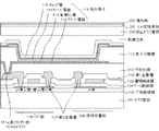
図1は、本発明の電気光学装置の一例としての有機EL表示装置を示している。この有機EL表示装置は、大別して、発光素子が形成されるTFT(Thin Film Transistor)基板100と、発光素子を封止する封止ガラス基板200と、TFT基板100と封止ガラス基板200とを接合する接合手段(ガラスフリットシール部)300などで構成される。また、TFT基板100の表示領域外側のカソード電極形成領域114aの周囲に、TFT基板100の走査線を駆動する走査ドライバ131、各画素の発光期間を制御するエミッション制御ドライバ132、静電気放電による破損を防ぐデータ線ESD(Electro-Static-Discharge)保護回路133、高転送レートのストリームを本来の低転送レートの複数のストリームに戻すデマルチプレクサ(1:n DeMUX134)、異方性導電フィルム(ACF:Anisotropic Conductive Film)を用いて実装される、データ線を駆動するデータドライバIC135などが配置され、FPC(Flexible Printed Circuit)136を介して外部の機器と接続される。なお、図1は、本実施形態の有機EL表示装置の一例であり、その形状や構成は適宜変更可能である。
FIG. 1 shows an organic EL display device as an example of the electro-optical device of the present invention. This organic EL display device is roughly divided into a TFT (Thin Film Transistor)
図2は、TFT基板100上に形成される発光素子の上下に隣り合う2つの画素(6つのサブ画素)に着目した平面図であり、この2つの画素からなる組が列方向(図の上下方向)に繰り返し配置される。また、図示しない隣の列では、上記2つの画素からなる組が上下方向に1画素分ずれて繰り返し配置される。すなわち、奇数列では奇数行と次の偶数行とで組を成し、偶数列では偶数行と次の奇数行とで組を成すように、2つの画素からなる組が、斜めに交い違いに配置される。また、図3は、1つのサブ画素に着目した断面図である。なお、図3では、本実施形態のサブ画素の構造を分かりやすくするために、図2の平面図の中のTFT部108b(M2駆動TFT)と保持容量部109の領域を抜き出し、簡略化して記載している。
FIG. 2 is a plan view paying attention to two pixels (six sub-pixels) adjacent to each other on the upper and lower sides of the light emitting element formed on the
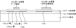
TFT基板100は、ガラス基板101上に下地絶縁膜102を介して形成された低温ポリシリコン(LTPS:Low-temperature poly silicon)等からなるポリシリコン層103と、ゲート絶縁膜104を介して形成された第1金属層105(ゲート電極105a及び保持容量電極105b)と、層間絶縁膜106に形成された開口を介してポリシリコン層103に接続される第2金属層107(データ線107a、電力供給線107b、ソース/ドレイン電極、第1コンタクト部107c)と、平坦化膜110を介して形成される発光素子116(アノード電極111、有機EL層113、カソード電極114及びキャップ層115)とで構成される。
The
上記発光素子116と封止ガラス基板200との間に乾燥空気が封入され、ガラスフリットシール部300により封止され、有機EL表示装置が形成される。この発光素子116はトップエミッション構造であり、発光素子116と封止ガラス基板200とは所定の間隔に設定されると共に、封止ガラス基板200の光出射面側にλ/4位相差板201と偏光板202とが形成され、外部から入射した光の反射が抑制されるようになっている。 Dry air is sealed between the light emitting element 116 and the sealing glass substrate 200 and sealed by the glass frit seal portion 300 to form an organic EL display device. The light emitting element 116 has a top emission structure, the light emitting element 116 and the sealing glass substrate 200 are set at a predetermined interval, and a λ / 4 phase difference plate 201 is provided on the light emission surface side of the sealing glass substrate 200. A polarizing plate 202 is formed, and reflection of light incident from the outside is suppressed.
図2において、一画素は、対向するデータ線107aと電力供給線107bとで挟まれた3つの領域で構成され、各々の領域に、スイッチTFT108a、駆動TFT108b及び保持容量部109が配置される。ここで、RGB縦ストライプ方式の画素配列構造の場合、アノード電極111が上記の3つの領域に分かれて形成され、各々の領域のスイッチTFT108a、駆動TFT108b及び保持容量部109を用いて、その領域に形成された発光素子116を駆動することになるが、本実施例では、RGB縦ストライプ方式と同様の構造で本実施形態の画素配列構造を実現するために、Rのサブ画素及びGのサブ画素のアノード電極111を2つの領域を跨ぐように形成する。
In FIG. 2, one pixel is composed of three regions sandwiched between opposing
具体的には、視感度が最も低い色であるBのサブ画素に関しては、アノード電極111(図2の太い実線)は主にBのデータ線107a及びBの電力供給線107bに沿って縦長に形成され、発光素子116は各画素の右側のB発光領域119(図2の太い破線)で発光する。一方、Rのサブ画素に関しては、アノード電極111がRのデータ線107aからGの電力供給線107bに渡る領域の上半分に形成されるため、発光素子116は各画素の左上のR発光領域117で発光する。また、視感度が最も高い色であるGのサブ画素に関しては、アノード電極111がRのデータ線107aからGの電力供給線107bに渡る領域の下半分に形成されるため、発光素子116は各画素の左下のG発光領域118で発光する。なお、本明細書及び請求の範囲における視感度最高色及び視感度最低色とは、相対的な意味であり、1画素の中で含まれる複数のサブ画素同士間で比較する場合の「最高」/「最低」を指す。
Specifically, for the B subpixel having the lowest visibility, the anode electrode 111 (thick solid line in FIG. 2) is vertically long mainly along the
すなわち、各色のサブ画素は、その色のデータ線107a及び電力供給線107bで囲まれる領域に形成されるスイッチTFT108a、駆動TFT108b及び保持容量部109を用いて駆動されるが、RとGのサブ画素のアノード電極111は、Rのデータ線107a及び電力供給線107bで囲まれる領域と、Gのデータ線107a及び電力供給線107bで囲まれる領域とを跨ぐように上下に分けて形成するため、アノード電極111と駆動TFT108bのソース/ドレイン電極とを繋ぐ第2コンタクト部111aは図のような配置となる。
That is, each color sub-pixel is driven using the
また、スイッチTFT108aはデータ線107aからのクロストークを抑えるため、図のようなデュアルゲート構造とする。電圧を電流に変換する駆動TFT108bは製造プロセスのばらつきを最小限に抑えるため、図のような引き回し形状とすることで十分なチャネル長を確保している。またこの駆動TFTのゲート電極を延長して保持容量部109の電極としても使うことで、限られた面積で十分な保持容量を確保することができる。このような画素構造とすることにより、RGB各色の発光領域を大きくできるため、必要輝度を得るための各色の単位面積あたりの電流密度を下げ、発光素子の長寿命化が可能となる。
The
なお、図3では、発光素子116の各放射光が、封止ガラス基板200を介して外部に放射されるトップエミッション構造を示したが、ガラス基板101を介して外部に放射されるボトムエミッション構造とすることもできる。 3 shows a top emission structure in which each radiated light of the light emitting element 116 is radiated to the outside through the sealing glass substrate 200, a bottom emission structure to be radiated to the outside through the glass substrate 101. It can also be.
ここで、本実施形態では、上下に隣接する2つのBのサブ画素に対してFMMの開口部を1つ設け、2つのBのサブ画素を跨ぐようにBの有機EL材料を堆積している。上側のBのサブ画素ではB発光領域119を下側に極力広げ、下側のBのサブ画素ではB発光領域119を上側に極力広げ、B発光領域119の形状を2つのBのサブ画素の中心線に対して線対称にすることで、B発光領域119の面積を大きくし、表示装置の長寿命化を図っている。 Here, in the present embodiment, one FMM opening is provided for two upper and lower adjacent B sub-pixels, and the B organic EL material is deposited so as to straddle the two B sub-pixels. . In the upper B sub-pixel, the B light-emitting region 119 is expanded as much as possible downward, and in the lower B sub-pixel, the B light-emitting region 119 is expanded as much as possible upward, and the shape of the B light-emitting region 119 is changed to the two B sub-pixels. By making the line symmetric with respect to the center line, the area of the B light emitting region 119 is increased, thereby extending the life of the display device.
このように2つのBのサブ画素はBの有機EL材料が連続しており、この2つの画素からなる組が列方向(図の上下方向)に繰り返し配置されると共に、図示しない隣の列では、上記2つの画素からなる組が上下方向に1画素分ずれて繰り返し配置される。そのため、表示素子の材料を分析してBの有機EL材料の堆積領域を調べることにより、本実施形態の画素配列構造であるかを判別することができる。また、B発光領域119の形状を観察することによっても、本実施形態の画素配列構造であるかを判別することが可能である。 In this way, the B organic EL material is continuous in the two B sub-pixels, and a set of these two pixels is repeatedly arranged in the column direction (vertical direction in the figure), and in the adjacent column (not shown). The set of two pixels is repeatedly arranged with a shift of one pixel in the vertical direction. Therefore, by analyzing the display element material and examining the deposition area of the B organic EL material, it is possible to determine whether the pixel arrangement structure of this embodiment is obtained. Further, by observing the shape of the B light emitting region 119, it is possible to determine whether the pixel arrangement structure of the present embodiment is obtained.
具体的には、図3に示すように、アノード電極111とM2駆動TFT(TFT部108b)のソース/ドレイン電極とを繋ぐ第2コンタクト部111aでは、アノード電極111は窪んだ形状(凹状)になるため、その上に均一に有機EL層113を形成することができない。そこで、アノード電極111上に形成する素子分離膜112は、第2コンタクト部111aに重ならない位置で除去して開口部を形成し、その開口部に有機EL層113とカソード電極114を形成して発光素子116として機能させている。そのため、発光素子116は、第2コンタクト部111a近傍を避けるように変形した形状になる。
Specifically, as shown in FIG. 3, in the second contact portion 111a that connects the
図4は、図2のアノード電極111と発光領域117〜119と第2コンタクト部111a(矩形の中に×印を付加した部分)を抜き出した図である。R発光領域117は、第2コンタクト部111aとの距離を十分に確保することができるため、ほぼ矩形状に形成される。また、G発光領域118も、第2コンタクト部111aとの距離を十分に確保することができるため、ほぼ矩形状に形成される。これに対して、B発光領域119は、装置の寿命を延ばすために極力面積を大きくする必要があり、その結果、第2コンタクト部111aに近づく部分が生じるため、第2コンタクト部111aとの距離が近い部分に窪み119aが形成される。そして、この窪み119aは、第2コンタクト部111aのレイアウト上、上側のB発光領域119では上辺部に、下側のB発光領域119では下辺部に形成される。
FIG. 4 is a diagram in which the
このように、本実施形態の画素アレイでは、組を成す2つの画素の上下のB発光領域119には、2つのBのサブ画素の中心線に対して線対称位置に窪み119aが形成されるため、この画素アレイを組み込んだ表示装置を形成した後においても、B発光領域119の形状を拡大して観察することにより、本実施形態の画素構造であるかを確認することが可能になる。なお、この窪み119aはB発光領域119に対して十分に小さいため、表示品質に影響を与えることはない。 As described above, in the pixel array according to the present embodiment, the depressions 119a are formed in line-symmetric positions with respect to the center line of the two B sub-pixels in the upper and lower B light emission regions 119 of the two pixels forming the set. Therefore, even after the display device incorporating the pixel array is formed, it is possible to confirm whether the pixel structure of the present embodiment is obtained by observing the B light emission region 119 in an enlarged manner. Note that the depression 119a is sufficiently small with respect to the B light emitting region 119, and thus does not affect the display quality.
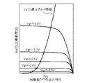
次に、各サブ画素の駆動方法について図5乃至図7を参照して説明する。図5はサブ画素の主要回路構成図であり、図6は波形図、図7は駆動TFTの出力特性図である。各サブ画素は、M1スイッチTFTと、M2駆動TFTと、C1保持容量と、発光素子(OLED)とを備えて構成されており、2トランジスタ方式により駆動制御される。M1スイッチTFTはpチャネル型FET(Field Effect Transistor)であり、そのゲート端子には走査線(Scan)が接続され、ドレイン端子にはデータ線(Vdata)が接続されている。M2駆動TFTはpチャネル型FETであり、そのゲート端子はM1スイッチTFTのソース端子に接続されている。また、M2駆動TFTのソース端子は電力供給線(VDD)に接続されており、ドレイン端子は発光素子(OLED)に接続されている。さらに、M2駆動TFTのゲート/ソース間にはC1保持容量が形成されている。 Next, a method for driving each sub-pixel will be described with reference to FIGS. FIG. 5 is a main circuit configuration diagram of the sub-pixel, FIG. 6 is a waveform diagram, and FIG. 7 is an output characteristic diagram of the driving TFT. Each subpixel includes an M1 switch TFT, an M2 drive TFT, a C1 storage capacitor, and a light emitting element (OLED), and is driven and controlled by a two-transistor method. The M1 switch TFT is a p-channel FET (Field Effect Transistor), a scanning line (Scan) is connected to the gate terminal, and a data line (Vdata) is connected to the drain terminal. The M2 drive TFT is a p-channel type FET, and its gate terminal is connected to the source terminal of the M1 switch TFT. The source terminal of the M2 driving TFT is connected to the power supply line (VDD), and the drain terminal is connected to the light emitting element (OLED). Further, a C1 storage capacitor is formed between the gate and source of the M2 drive TFT.
上記の構成において、走査線(Scan)に選択パルスを出力し、M1スイッチTFTを開状態にすると、データ線(Vdata)を介して供給されたデータ信号は電圧値としてC1保持容量に書き込まれる。C1保持容量に書き込まれた保持電圧は1フレーム期間を通じて保持され、当該保持電圧によって、M2駆動TFTのコンダクタンスがアナログ的に変化し、発光諧調に対応した順バイアス電流を発光素子(OLED)に供給する。 In the above configuration, when a selection pulse is output to the scanning line (Scan) and the M1 switch TFT is opened, the data signal supplied via the data line (Vdata) is written to the C1 storage capacitor as a voltage value. The holding voltage written in the C1 holding capacitor is held throughout one frame period, and the conductance of the M2 driving TFT changes in an analog manner by the holding voltage, and a forward bias current corresponding to the light emission gradation is supplied to the light emitting element (OLED). To do.
このように、発光素子(OLED)を定電流で駆動することにより、発光素子(OLED)の劣化によって抵抗が変化しても発光輝度を一定に保つことができる。そのため、本実施形態の有機EL表示装置の駆動方法として好適である。 In this way, by driving the light emitting element (OLED) with a constant current, the light emission luminance can be kept constant even when the resistance changes due to deterioration of the light emitting element (OLED). Therefore, it is suitable as a driving method for the organic EL display device of this embodiment.
次に、上記構造の有機EL表示装置の画素配列構造について、図8乃至図10を参照して説明する。なお、図8乃至図10に示すRGBのサブ画素は、発光素子として機能する発光領域(図3において有機EL層113がアノード電極111とカソード電極114に挟まれた部分)を示している。この発光領域は、素子分離膜112の開口部を示している。FMMを用いて有機EL材料を選択的に堆積させる場合には、この発光領域よりやや大きめの開口部を有するFMMをTFT基板にアライメントしてセットして選択的に有機EL材料を堆積させる。実際に電流が流れるのは素子分離膜112の開口部のみであるので、この部分が発光領域となる。FMMの開口部パターンが他の色の開口部に重なると(すなわち、有機EL材料を堆積させる領域が広がってしまうと)、他の発光色が混ざる不良(色ずれ)が生じる。また、開口部より内側に入ってしまうと(すなわち、有機EL材料を堆積させる領域が狭まってしまうと)、アノード電極111とカソード電極114とがショートしてしまう不良(上下ショート不良)が生じる危険性がある。従って、FMMの開口パターンは、概ね自色の発光領域の外側で他色の発光領域までのほぼ中間の境界線上に開口するように設計される。FMMのアライメント精度や変形量はフォトプロセスの精度に比べると悪いが、実際の発光領域はフォトプロセスによって開口される発光領域によって決定されるので、どのような形状であっても正確に面積を制御することができる。また、図8乃至図10における各画素の境界線(実線)は、TFT基板100の構成部材によって規定されるものではなく、サブ画素の組を繰り返し配置した場合における隣り合うサブ画素の組との関係で規定されるものであり、ここでは矩形としているが、矩形以外の形状でもよい。
Next, a pixel arrangement structure of the organic EL display device having the above structure will be described with reference to FIGS. Note that the RGB sub-pixels illustrated in FIGS. 8 to 10 indicate a light-emitting region functioning as a light-emitting element (a portion where the organic EL layer 113 is sandwiched between the
図8に示すように、本実施形態の画素配列の基本構造は、図38に示すSストライプ方式の画素配列構造(Rのサブ画素とGのサブ画素とが列方向に配列され、Bのサブ画素がRのサブ画素及びGのサブ画素に対して行方向に配置される画素配列構造)において、奇数列に関しては奇数行と次の偶数行の2つの画素を1組とし、偶数列に関しては偶数行と次の奇数行の2つの画素を1組とし、各組の2つの画素のBのサブ画素の有機EL材料が連続し、各組の2つの画素のBのサブ画素の発光領域が2つの画素の中心線に対して線対称な構造である。なお、同じ組の2つのBのサブ画素は別々に駆動されるためにアノード電極111は分離しており、図4に示すように、アノード電極111とTFT部108(M2駆動TFT)のドレイン端子とを接続する第2コンタクト部111aは2つのBのサブ画素の中心線に対して線対称に配置され、第2コンタクト部111aが配置される部分近傍でB発光領域119に窪み119aが生じるため、各々のBのサブ画素の発光領域119は、厳密には、2つのBのサブ画素の中心線に対して窪み119aが線対称に形成された形状となるが、図8では、各サブ画素の発光領域を略矩形形状としている。
As shown in FIG. 8, the basic structure of the pixel arrangement of the present embodiment is the S stripe type pixel arrangement structure shown in FIG. 38 (R subpixels and G subpixels are arranged in the column direction, and B subpixels are arranged). In the pixel arrangement structure in which the pixels are arranged in the row direction with respect to the R sub-pixel and the G sub-pixel), the odd-numbered column and the next even-numbered row are set as one set for the odd-numbered column, and the even-numbered column is set The two pixels in the even numbered row and the next odd numbered row are made into one set, and the organic EL material of the B subpixel of the two pixels in each set is continuous, and the light emission area of the B subpixel of the two pixels in each set is This is a line-symmetric structure with respect to the center line of two pixels. Note that the
図8において、上述したように、有機EL材料の堆積領域はFMMの開口部によって規定され、発光領域は素子分離膜112の開口部によって規定されが、素子分離膜112の開口部は、アノード電極111とカソード電極114とのショート及び他の発光色が混ざる色ずれを防止するために、製造プロセスの精度で規定されるマージンを見込んで、有機EL材料の堆積領域よりも内側に形成される。また、同じBの有機EL材料の堆積領域において、2つのBの発光領域も、製造プロセスの精度で規定されるマージンを見込んで、所定の間隔を空けて形成される。従って、Bの有機EL材料の堆積領域内で2つのBの発光領域を最大にした場合(開口率を優先した場合)、Bの発光領域は図8のような形状になる。
In FIG. 8, as described above, the deposition region of the organic EL material is defined by the opening of the FMM, and the light emitting region is defined by the opening of the element isolation film 112. The opening of the element isolation film 112 is the anode electrode. In order to prevent a short circuit between 111 and the
図8の下図は、2×2の4画素を拡大した図である。4画素の内の右上の画素及び左下の画素は、Bの発光領域を最大にするためにBの発光領域が下側に広がり、その結果、その中心位置が下側(視感度が最も高いGの発光領域に近づく方向)に移動し、Bの発光領域の中心位置とGの発光領域の中央位置の列方向の間隔はr1となる。一方、左上の画素及び右下の画素は、Bの発光領域を最大にするためにBの発光領域が上側に広がり、その結果、その中心位置が上側(Gの発光領域から遠ざかる方向)に移動し、Bの発光領域の中心位置とGの発光領域の中央位置の列方向の間隔はr1よりも大きいr2となる。 The lower diagram of FIG. 8 is an enlarged view of 2 × 2 four pixels. Among the four pixels, the upper right pixel and the lower left pixel have the B light emission region spread downward to maximize the B light emission region, and as a result, the center position is lower (G having the highest visibility). The distance in the column direction between the center position of the B light emission area and the center position of the G light emission area is r1. On the other hand, in the upper left pixel and the lower right pixel, in order to maximize the B light emission area, the B light emission area expands upward, and as a result, the center position moves upward (in a direction away from the G light emission area). The distance in the column direction between the central position of the B light emitting region and the central position of the G light emitting region is r2, which is larger than r1.
ここで、図43に示す従来の画素配列構造では、図43の下図に示すように、上側の画素は共にBの発光領域の中心位置とGの発光領域の中央位置の列方向の間隔はr1となり、下側の画素は共にBの発光領域の中心位置とGの発光領域の中央位置の列方向の間隔はr1よりも大きいr2となるため、上記間隔が大きい下側の画素において視感度の分布の偏りが大きくなり、下側の画素が表示画像のエッジになる場合に色付きが顕著に現れ、表示品質を著しく悪化させていた。これに対して、本実施形態の画素配列構造では、上記間隔が大きい画素が連続せず、間隔が大きい画素と間隔が小さい画素とが交互に出現するため、視感度の分布の偏りを平均化することができ、その結果、色付きの発生を抑制して表示品質を向上させることができる。 Here, in the conventional pixel array structure shown in FIG. 43, as shown in the lower diagram of FIG. 43, the upper pixel has an interval in the column direction between the center position of the B light emitting region and the center position of the G light emitting region. In the lower pixel, the column-wise interval between the center position of the B light emitting region and the center position of the G light emitting region is r2 which is larger than r1, and therefore the visibility of the lower pixel having the large interval is low. When the distribution becomes large and the lower pixel becomes the edge of the display image, coloring is noticeable and the display quality is remarkably deteriorated. On the other hand, in the pixel arrangement structure of the present embodiment, pixels with large intervals are not continuous, and pixels with large intervals and pixels with small intervals appear alternately. As a result, generation of coloring can be suppressed and display quality can be improved.
上記図8の画素配列構造を採用することにより、従来構造に比べて色付きの発生を抑制することはできる。また、Bの発光領域のサイズや位置を調整することによって、色付きの発生を更に抑制することができる。 By adopting the pixel arrangement structure shown in FIG. 8, the occurrence of coloring can be suppressed as compared with the conventional structure. Further, the occurrence of coloring can be further suppressed by adjusting the size and position of the light emitting region of B.
図9は、Bの発光領域のサイズを調整する場合の例である。例えば、図9に示すように、Bの有機EL材料の堆積領域は変えずに、Bの発光領域の中心位置とGの発光領域の中央位置の列方向の間隔が上下の画素で近づくように(すなわち、上下の画素の対称性を優先して)、各々のBの発光領域のサイズを小さくする。この場合、図9の下図に示すように、4画素の内の右上の画素及び左下の画素の、Bの発光領域の中心位置とGの発光領域の中央位置の列方向の間隔r1’と、左上の画素及び右下の画素の、Bの発光領域の中心位置とGの発光領域の中央位置の列方向の間隔r2’と、はほぼ等しくなる。従って、r1’とr2’との差(r2’−r1’)は図8のr1とr2との差(r2−r1)よりも小さくなり色付きの発生を更に抑制することができる。この構造の場合、Bの発光領域が小さくなって表示装置の寿命は短くなるため、どの程度対称性を優先する(Bの発光領域のサイズを小さくする)かは、色付きの程度を勘案して適宜設定することができる。 FIG. 9 shows an example of adjusting the size of the B light emitting area. For example, as shown in FIG. 9, without changing the deposition region of the organic EL material of B, the interval in the column direction between the center position of the B light emission region and the center position of the G light emission region is made closer to the upper and lower pixels. (In other words, the symmetry of the upper and lower pixels is prioritized), and the size of each B light emitting region is reduced. In this case, as shown in the lower diagram of FIG. 9, an interval r1 ′ in the column direction between the center position of the B emission region and the center position of the G emission region of the upper right pixel and the lower left pixel of the four pixels, The distance r2 ′ in the column direction between the center position of the B light emission region and the center position of the G light emission region of the upper left pixel and the lower right pixel is substantially equal. Therefore, the difference (r2'-r1 ') between r1' and r2 'becomes smaller than the difference (r2-r1) between r1 and r2 in Fig. 8, and the occurrence of coloring can be further suppressed. In the case of this structure, the light emission region of B becomes small and the lifetime of the display device is shortened. Therefore, how much symmetry is prioritized (the size of the light emission region of B is reduced) is taken into account the degree of coloring. It can be set appropriately.
図10は、Bの発光領域の位置を調整する場合の例である。例えば、図10に示すように、Bの有機EL材料の堆積領域のサイズは変えずに、その位置を下側にずらす。具体的には、図10の下図に示すように、Bの有機EL材料の堆積領域の上端と上側の画素の境界との距離a1を、下端と下側の画素の境界との距離a2よりも大きくする。この場合、4画素の内の右上の画素及び左下の画素は、Bの発光領域の中心が下に移動し、Bの発光領域の中心位置とGの発光領域の中央位置の列方向の間隔r1”は図8のr1よりも小さくなる。また、左上の画素及び右下の画素も、Bの発光領域の中心位置とGの発光領域の中央位置の列方向の間隔r2”は図8のr2よりも小さくなる。従って、r1”とr2”は共に図8のr1とr2よりも小さくなるため、色付きの発生を更に抑制することができる。この構造の場合、Bの発光領域がずれることによって視感度の分布に偏りが生じるため、Bの発光領域の位置をどの程度ずらすかは、色付きの程度を勘案して適宜設定することができる。 FIG. 10 shows an example of adjusting the position of the B light emitting region. For example, as shown in FIG. 10, the position of the B organic EL material deposition region is shifted downward without changing the size of the deposition region. Specifically, as shown in the lower diagram of FIG. 10, the distance a1 between the upper end of the B organic EL material deposition region and the upper pixel boundary is set to be larger than the distance a2 between the lower end and the lower pixel boundary. Enlarge. In this case, in the upper right pixel and the lower left pixel among the four pixels, the center of the B light emission region moves downward, and the column direction interval r1 between the center position of the B light emission region and the center position of the G light emission region. 8 is smaller than r1 in FIG. 8. Also, in the upper left pixel and the lower right pixel, the column position interval r2 between the center position of the B light emitting region and the central position of the G light emitting region is r2 in FIG. Smaller than. Therefore, since r1 ″ and r2 ″ are both smaller than r1 and r2 in FIG. 8, the occurrence of coloring can be further suppressed. In the case of this structure, the visibility distribution is biased due to the deviation of the B light emission region, and therefore, how much the position of the B light emission region is shifted can be appropriately set in consideration of the degree of coloring.
なお、図8乃至図10では、上下の画素における、Bの発光領域の中心位置とGの発光領域の中央位置との間隔を比較したが、Bの発光領域の中心位置と画素の重心(RGBの発光領域の中心位置)との間隔を比較してもよい。また、図9ではBの発光領域のサイズを調整し、図10ではBの発光領域の位置を調整したが、r2とr1の差が小さくなる、若しくは、r2とr1とが共に小さくなるような画素配列構造であればよい。 8 to 10, the distance between the center position of the B light emitting region and the center position of the G light emitting region in the upper and lower pixels is compared. However, the center position of the B light emitting region and the center of gravity of the pixel (RGB The distance from the center position of the light emitting region) may be compared. In FIG. 9, the size of the B light emitting region is adjusted, and in FIG. 10, the position of the B light emitting region is adjusted. However, the difference between r2 and r1 is small, or both r2 and r1 are small. Any pixel arrangement structure may be used.
次に、本発明の第1の実施例に係る表示デバイス及び電気光学装置について、図11乃至図27を参照して説明する。 Next, a display device and an electro-optical device according to the first embodiment of the invention will be described with reference to FIGS.
前記した実施形態では、本発明の電気光学装置(有機EL表示装置)の画素配列構造に着目して説明したが、本実施例では、この画素配列構造の画素アレイを備えた有機EL表示装置の製造方法について説明する。なお、図11、13、15、17は図10の画素配列構造の内の一組の画素の平面図であり、図12、14、16、18は一つのサブ画素に着目したTFT部、保持容量部及び発光素子の断面図である。 In the above-described embodiment, the description has been given focusing on the pixel array structure of the electro-optical device (organic EL display device) of the present invention. However, in this embodiment, the organic EL display device including the pixel array having the pixel array structure is described. A manufacturing method will be described. 11, 13, 15, and 17 are plan views of a set of pixels in the pixel arrangement structure of FIG. 10, and FIGS. 12, 14, 16, and 18 are TFT portions that focus on one sub-pixel, holding It is sectional drawing of a capacity | capacitance part and a light emitting element.
まず、図11及び図12に示すように、ガラス等の透光性の基板(ガラス基板101)上にCVD(Chemical Vapor Deposition)法等によって、例えばシリコン窒化膜等を堆積して下地絶縁膜102を形成する。次に、公知の低温ポリシリコンTFT製造技術を用いて、TFT部及び保持容量部を形成する。具体的には、CVD法等によってアモルファスシリコンを堆積し、ELA(Excimer Laser Annealing)により結晶化してポリシリコン層103を形成する。その際、電圧電流変換増幅器として用いるM2駆動TFTのチャネル長を十分長く確保して出力電流のばらつきを抑え、M1スイッチTFTのソースとデータ線107aとの接続、M1スイッチTFTのドレインとC1保持容量との接続、C1保持容量と電力供給線107bとの接続、M2駆動TFTのソースと電力供給線107bとの接続、M2駆動TFTのドレインと各サブ画素のアノード電極111との接続を可能にするために、図のようにポリシリコン層103を引き回している。また、行毎にY軸対称構造にするために、図の上側と下側とでM1スイッチTFT、M2駆動TFT、C1保持容量の形状を変更している。なお、図では、M1スイッチTFT、M2駆動TFT、C1保持容量の位置を明確にするために、画素の境界を一点鎖線で示し、アノード電極111を実線、R発光領域117、G発光領域118、B発光領域119を破線で示している。
First, as shown in FIGS. 11 and 12, for example, a silicon nitride film or the like is deposited on a light-transmitting substrate (glass substrate 101) such as glass by a CVD (Chemical Vapor Deposition) method or the like to form a base insulating film 102. Form. Next, a TFT part and a storage capacitor part are formed using a known low-temperature polysilicon TFT manufacturing technique. Specifically, amorphous silicon is deposited by a CVD method or the like, and crystallized by ELA (Excimer Laser Annealing) to form a
次に、図13及び図14に示すように、ポリシリコン層103上にCVD法等によって、例えばシリコン酸化膜等を堆積してゲート絶縁膜104を形成し、更に、スパッタ法等により第1金属層105としてMo(モリブデン)やNb(ニオブ)、W(タングステン)との合金等を堆積してゲート電極105a及び保持容量電極105bを形成する。また、本実施例では、後述する第2金属層107で形成する電力供給線107b同士を接続するために、ゲート電極105aと同層に、ゲート電極105aの方向に延在する電力供給線105cを形成する。なお、第1金属層105は、例えばMo、W、Nb、MoW、MoNb、Al、Nd、Ti、Cu、Cu合金、Al合金、Ag、Ag合金などからなる群より選択される一つの物質で単一層を形成したり、配線抵抗を減少させるために低抵抗物質であるMo、Cu、AlまたはAgの2層構造またはそれ以上の多重膜構造からなる群より選択される一つの積層構造で形成したりしても良い。その際、各サブ画素における保持容量を大きくすると共に、各サブ画素のM1スイッチTFTのドレインと保持容量電極105bとの接続を容易にするために、図のような形状で第1金属層105を形成している。次に、ゲート電極形成前に高濃度不純物層(p+層103c)をドーピングしておいたポリシリコン層103に、ゲート電極105aをマスクとして追加不純物ドーピングを施して低濃度不純物層(p−層103b)を形成することにより、TFT部にLDD(Lightly Doped Drain)構造を形成する。
Next, as shown in FIGS. 13 and 14, for example, a silicon oxide film or the like is deposited on the
次に、図15及び図16に示すように、CVD法等によって、例えばシリコン酸化膜等を堆積して層間絶縁膜106を形成する。この層間絶縁膜106及びゲート絶縁膜104に異方性エッチングを行い、ポリシリコン層103に接続するためのコンタクトホール及び電力供給線105cに接続するためのコンタクトホールを開口する。次に、スパッタ法等によって、例えばTi/Al/Ti等のアルミ合金の第2金属層107を堆積し、パターニングを行ってソース/ドレイン電極、データ線107a、電力供給線107b、第1コンタクト部107c(黒塗りの矩形部分)を形成する。その際、電力供給線107bは直線状に形成すると共に、第1コンタクト部107cを介して所定の電力供給線105cに接続する。また、Bの電力供給線107bは、R及びGの電力供給線107bよりも幅を広くする。また、データ線107aは行毎にサブ画素の右側又は左側に配置されるように引き回した形状にする。これにより、データ線107aとM1スイッチTFTのソース、M1スイッチTFTのドレインと保持容量電極105b及びM2駆動TFTのゲート、M2駆動TFTのソースと電力供給線107bとが接続される。
Next, as shown in FIGS. 15 and 16, for example, a silicon oxide film or the like is deposited by CVD or the like to form an
次に、図17及び図18に示すように、感光性の有機材料を堆積し平坦化膜110を形成する。そして、露光条件を最適化してテーパー角を調整し、M2駆動TFTのドレインに接続するためのコンタクトホール(×印を付した太い実線の部分)を開口する。このコンタクトホールの開口は、2つのBのサブ画素の中心線に対して、線対称位置に形成される。この上にAg、Mg、Al、Pt、Pd、Au、Ni、Nd、Ir、Crおよびこれらの化合物金属で反射膜を堆積し、その上に続けてITO、IZO、ZnO、In2O3等の透明膜を堆積し、同時にパターニングして各サブ画素のアノード電極111を形成する。アノード電極111は第2コンタクト部111aでM2駆動TFTのドレインと接続される。なお、アノード電極111は、トップエミッション構造の場合は反射膜としても機能させるため反射膜が必要だが、ボトムエミッション構造の場合には反射膜を省き、ITO等の透明膜のみで形成する。次に、スピンコート法等によって、例えば感光性の有機樹脂膜を堆積して素子分離膜112を形成し、パターニングを行って、各サブ画素のアノード電極111を底部に露出させた素子分離層を形成する。この素子分離層により、各サブ画素の発光領域が分離される。
Next, as shown in FIGS. 17 and 18, a photosensitive organic material is deposited to form a planarization film 110. Then, a taper angle is adjusted by optimizing the exposure conditions, and a contact hole (a thick solid line portion marked with x) is opened to connect to the drain of the M2 driving TFT. The contact hole opening is formed at a line-symmetrical position with respect to the center line of the two B sub-pixels. On this, a reflective film is deposited with Ag, Mg, Al, Pt, Pd, Au, Ni, Nd, Ir, Cr and their compound metals, followed by ITO, IZO, ZnO, In 2 O 3 and the like. The transparent film is deposited and simultaneously patterned to form the
次に、素子分離膜112を形成したガラス基板101に対して有機EL材料を成膜する。図19乃至図21は、この有機EL材料の成膜に際して使用するメタルマスクの製造方法であり、有機ELパネルの端部近傍の領域を示している。また、図22乃至図24は、各色の有機EL材料を成膜するためのメタルマスクの一部を示す平面図であり、図25及び図26は、このメタルマスクを用いた有機EL材料の成膜方法を模式的に示す断面図、図27は、メタルマスク本体と補強部材の位置関係を示す斜視図である。 Next, an organic EL material is formed on the glass substrate 101 on which the element isolation film 112 is formed. FIG. 19 to FIG. 21 show a method for manufacturing a metal mask used for film formation of the organic EL material, and shows a region near the end of the organic EL panel. FIGS. 22 to 24 are plan views showing a part of a metal mask for depositing the organic EL material of each color. FIGS. 25 and 26 show the formation of the organic EL material using the metal mask. FIG. 27 is a perspective view schematically showing the positional relationship between the metal mask main body and the reinforcing member.
まず、メタルマスクの製造方法について説明する。このメタルマスクは、型抜きやエッチングにより、薄板状のメタルマスク部材のサブ画素に対応する部分に開口部を形成することによっても製造可能であるが、ここではメッキ法を用いて説明する。具体的には、図19に示すように、メタルマスク本体をメッキ成長させるための母材(電鋳用母材145)を用意する。この電鋳用母材145の材料は特に限定されないが、少なくとも電解メッキのための電流を流すことができる導電性を有し(無電解メッキの場合は不要)、かつ、凹凸を切削やエッチングなどの方法で形成可能な材料(例えば、ガラス材やアルマイト等)を用いることができる。 First, a method for manufacturing a metal mask will be described. This metal mask can be manufactured by forming an opening in a portion corresponding to a sub-pixel of a thin metal mask member by die cutting or etching, but here, description will be made using a plating method. Specifically, as shown in FIG. 19, a base material (electroforming base material 145) for plating growth of the metal mask main body is prepared. The material of the base material for electroforming 145 is not particularly limited, but has at least conductivity that allows a current for electrolytic plating to flow (not required in the case of electroless plating), and cuts or etches unevenness. A material that can be formed by this method (for example, a glass material or anodized) can be used.
そして、ガイド部142を形成する部分(すなわち、有機ELパネルの画素領域の外側の部分)に突起142aを形成し、必要に応じて、メタルマスク部材141aの剥離を容易にするための黒鉛や導電性接着剤などを塗布したり被膜をメッキ成長させたりして下地を形成し、電鋳用母材145の全面にフォトレジストを塗布し、各画素内のサブ画素に対応する部分にフォトレジスト146が残るように露光、現像を行う。その際、メッキでは電鋳用母材145から成長したメタルマスク部材141aがフォトレジスト146を覆うように成長するため、フォトレジスト146を覆う量を考慮してフォトレジストパターンのサイズを決定すると共に、フォトレジスト146の厚みやメッキ成長の条件を設定する。
Then, a protrusion 142a is formed on a portion where the
次に、フォトレジスト146を形成した電鋳用母材145を電解液に浸け、電解メッキの場合は所定の電流を流して、図20に示すように、電鋳用母材145上に所定の厚さのメタルマスク部材141aを成長させる。メタルマスク部材141aは、例えば、ニッケル、ニッケル合金、ニッケル・コバルト合金、インバールなどのニッケル・鉄合金などとすることができる。なお、メタルマスク部材141aのメッキ成長に際し、特開2005−206881号公報に示すように、フォトレジストの厚みまで第1の金属を形成し、その上に第2の金属を形成する手法などを用いることも可能である。 Next, the electroforming base material 145 on which the photoresist 146 is formed is immersed in an electrolytic solution, and in the case of electrolytic plating, a predetermined current is passed, and a predetermined current is applied on the electroforming base material 145 as shown in FIG. A metal mask member 141a having a thickness is grown. The metal mask member 141a may be, for example, nickel, a nickel alloy, a nickel / cobalt alloy, a nickel / iron alloy such as Invar, or the like. In the plating growth of the metal mask member 141a, as shown in Japanese Patent Application Laid-Open No. 2005-206881, a method of forming the first metal up to the thickness of the photoresist and forming the second metal thereon is used. It is also possible.
メッキ成長後、メタルマスク部材141aを成長させた電鋳用母材145を所定の剥離液(例えば、アセトンや塩化メチル等)に浸して、電鋳用母材145からフォトレジスト146と共にメタルマスク部材141aを分離して、図21に示すような、サブ画素に対応する開口部143とガイド部142とが形成されたメタルマスク本体141が完成する。図22は、Rのサブ画素に対応するR開口部143aを形成したメタルマスク本体141、図23は、Gのサブ画素に対応するG開口部143bを形成したメタルマスク本体141、図24は、Bのサブ画素に対応するB開口部143cを形成したメタルマスク本体141の一例である。本実施例では、Bのサブ画素は上下に隣り合う2つの画素を跨ぐように開口部を形成するため、B開口部143cは、R開口部143aやG開口部143bに比べてサイズが大きくなるが、B開口部143cは、奇数行と偶数行とで1行分ずれた斜交いになり、行方向(図の左右方向)に関して開口部のエッジが一直線にならないため、メタルマスクの変形を抑制することができる。
After plating growth, the electroforming base material 145 on which the metal mask member 141a is grown is immersed in a predetermined stripping solution (for example, acetone, methyl chloride, etc.), and the metal mask member together with the photoresist 146 from the electroforming base material 145 By separating 141a, a metal mask body 141 in which an opening 143 and a
その後、図25乃至図27に示すように、メタルマスク本体141のガイド部142で規定される部分に所定の特性(強度、熱膨張率及び磁性)を有する補強部材144を位置合わせして配置し、TFT基板100の表面(上記バンク層が形成された成膜面)に補強部材144を配置したメタルマスク本体141を位置合わせして配置し、TFT基板100の裏面の補強部材144に対向する位置にマグネットなどの固定部材150を配置することによって、メタルマスク140をTFT基板100に固定する。そして、TFT基板100の表面を下にして蒸着装置の真空槽内のステージ160にセットし、るつぼ161を加熱して蒸着材162としての有機EL材料を蒸発させ、メタルマスク本体141の開口部143を介して、TFT基板100の各サブ画素に対応する位置に有機EL材料を蒸着させる。この補強部材を配置するのは、隣接する有機ELパネル作成領域の中間部である。ここには開口パターンを配置していないため、補強部材によって開口パターンが影響を受けることはない。このような構造を採用することによってメタルマスクの変形を抑制し、メタルマスクの取り付けに要する時間とコストを削減し、更に、メタルマスクの位置ズレや反りなどを簡単に修復できるようにする。
Thereafter, as shown in FIGS. 25 to 27, a reinforcing member 144 having predetermined characteristics (strength, coefficient of thermal expansion and magnetism) is positioned and arranged at a portion defined by the
なお、上記では、メタルマスク本体141のTFT基板100と反対側の面が突出するようにガイド部142を形成したが、TFT基板100と反対側の面が窪むようにガイド用の凹部を形成し、補強部材144に設けた凸部と係合するようにしてもよい。また、上記では、補強部材144や固定部材150の断面を矩形形状としたが、断面形状は図の構成に限定されず、例えば、台形形状や半円形状などとすることもできる。また、メタルマスク本体141がTFT基板100の全面に接触しないように、有機ELパネル形成領域の外側の所定の部分に、TFT基板100側に突出する凸部を設け、この凸部のみでメタルマスク本体141がTFT基板100に接触するようにしてもよい。また、上記では、メタルマスク本体141の製造方法の一例として、メッキ法を用いて説明したが、エッチング法を用いてもよい。
In the above description, the
図17及び図18に戻って、RGBの色毎に、有機EL材料を成膜して、アノード電極111上に、有機EL層113を形成する。その際、R及びBの有機EL材料は、左右に隣接する2つサブ画素に渡って堆積されるが、各々の色のアノード電極111は各サブ画素のM2スイッチTFTに接続されるため、画素を跨いで有機EL層113を形成しても問題はない。また、Bの有機EL材料も、上下に隣接する2つサブ画素に渡って堆積されるが、アノード電極111はサブ画素毎に分離しており、アノード電極111がない部分の有機EL材料は発光に寄与しないため、画素を跨いで有機EL層113を形成しても問題はない。この有機EL層113は、下層側から、例えば正孔注入層、正孔輸送層、発光層、電子輸送層、電子注入層などによって構成される。また、有機EL層113は、電子輸送層/発光層/正孔輸送層、電子輸送層/発光層/正孔輸送層/正孔注入層、電子注入層/電子輸送層/発光層/正孔輸送層あるいは発光層単独のいずれの構造でもよく、電子ブロッキング層等を追加してもよい。発光層の材質はサブ画素の色毎に異なり、必要に応じて正孔注入層や正孔輸送層等の膜厚もサブ画素毎に個別に制御する。
Referring back to FIGS. 17 and 18, an organic EL material is formed for each of RGB colors, and the organic EL layer 113 is formed on the
この有機EL層113の上に仕事関数が小さな金属、すなわちLi、Ca、LiF/Ca、LiF/Al、Al、Mg及びこれらの化合物を蒸着してカソード電極114を形成する。カソード電極の膜厚は光取り出し効率を向上させ良好な視野角依存性を確保するため最適化される。カソード電極の抵抗が高く発光輝度の均一性が損なわれる場合には、その上にITO、IZO、ZnOまたはIn2O3などの透明電極形成用の物質で補助電極層を追加する。さらに光取り出し効率向上のため、ガラスより屈折率の高い絶縁膜を堆積させキャップ層115を形成する。キャップ層は有機EL素子の保護層としての役割も果たす。
On the organic EL layer 113, a metal having a small work function, that is, Li, Ca, LiF / Ca, LiF / Al, Al, Mg, and a compound thereof are deposited to form the
以上により、RGBの各サブ画素に対応する発光素子116が形成され、アノード電極111と有機EL層113とが接触した部分(素子分離膜112の開口部分)が各々、R発光領域117、G発光領域118、B発光領域119となる。
As described above, the light emitting elements 116 corresponding to the RGB sub-pixels are formed, and the portions where the
なお、発光素子116をボトムエミッション構造とする場合は、平坦化膜110の上層にカソード電極114(ITOなどの透明電極)を形成し、有機EL層113の上に、アノード電極111(反射電極)を形成すればよい。ボトムエミッション構造では光を上面に取り出す必要が無いため、Al等の金属膜を厚く形成することができ、カソード電極の抵抗値を大幅に減少させることができるため大型化に適しているが、TFT素子や配線部分は光が透過できないため、発光領域が極端に小さくなり高精細化には適していない。 When the light emitting element 116 has a bottom emission structure, a cathode electrode 114 (a transparent electrode such as ITO) is formed on the planarizing film 110 and an anode electrode 111 (a reflective electrode) is formed on the organic EL layer 113. May be formed. The bottom emission structure does not require light to be extracted from the top surface, so that a metal film such as Al can be formed thick, and the resistance value of the cathode electrode can be greatly reduced. Since the element and the wiring part cannot transmit light, the light emitting region becomes extremely small and is not suitable for high definition.
次に、TFT基板100の外周にガラスフリットを塗設し、その上に封止ガラス基板200を載置し、ガラスフリット部をレーザー等を用いて加熱し、溶融させTFT基板100と封止ガラス基板200を密封する。その後、封止ガラス基板200の光出射側にλ/4位相差板201、偏光板202を形成し、有機EL表示装置が完成する。
Next, a glass frit is applied to the outer periphery of the
なお、図11乃至図27は、本実施例での有機EL表示装置の製造方法の一例であり、実施形態で示した画素配列構造が実現可能であれば、その製造方法は特に限定されない。 11 to 27 show an example of a method for manufacturing an organic EL display device in this example, and the method for manufacturing the organic EL display device is not particularly limited as long as the pixel arrangement structure described in the embodiment can be realized.
次に、本発明の第2の実施例に係る電気光学装置及び電気機器について、図28乃至図31を参照して説明する。本実施例では、有機EL表示装置の応用例として、有機EL表示装置を表示手段として備えた各種電気機器について説明する。 Next, an electro-optical device and an electric apparatus according to the second embodiment of the present invention will be described with reference to FIGS. In this embodiment, various electric devices including the organic EL display device as display means will be described as application examples of the organic EL display device.
図28乃至図31は、本発明の電気光学装置(有機EL表示装置)を適用可能な電気機器の例を示している。図28は、パーソナルコンピュータへの適用例、図29は、PDA(Personal Digital Assistants)や電子手帳、電子ブック、タブレット端末などの携帯端末機器への適用例、図30は、スマートフォンへの適用例、図31は携帯電話機への適用例である。これらの電気機器の表示部に、本発明の有機EL表示装置を利用することができる。なお、電気機器としては、表示装置を備えるものであれば特に限定はなく、例えば、デジタルカメラ、ビデオカメラ、ヘッドマウントディスプレイ、プロジェクタ、ファックス装置、携帯型TV、DSP(Demand Side Platform)装置などに適用することができる。 FIG. 28 to FIG. 31 show examples of electric equipment to which the electro-optical device (organic EL display device) of the present invention can be applied. FIG. 28 shows an application example to a personal computer, FIG. 29 shows an application example to a portable terminal device such as a PDA (Personal Digital Assistants), electronic notebook, electronic book, or tablet terminal, and FIG. 30 shows an application example to a smartphone. FIG. 31 shows an example applied to a mobile phone. The organic EL display device of the present invention can be used for the display portion of these electric devices. The electrical equipment is not particularly limited as long as it is provided with a display device. For example, the electronic device may be a digital camera, a video camera, a head mounted display, a projector, a fax device, a portable TV, a DSP (Demand Side Platform) device, or the like. Can be applied.
次に、本発明の第3の実施例に係る電気光学装置及び電気機器について、図32乃至図35を参照して説明する。前記した第2の実施例では、本発明の電気光学装置としての有機EL表示装置を平面状の表示部を備える電気機器に適用する場合について説明したが、有機EL表示装置を変形可能な構造にすることにより、曲面状の表示部を必要とする電気機器に適用することができる。 Next, an electro-optical device and an electric apparatus according to the third embodiment of the present invention will be described with reference to FIGS. In the second embodiment described above, the case where the organic EL display device as the electro-optical device of the present invention is applied to an electric apparatus having a flat display portion has been described. However, the organic EL display device has a deformable structure. By doing so, it can be applied to an electric device that requires a curved display portion.
図32は、変形可能な有機EL表示装置の構造を示す断面図である。前記した第1の実施例と異なる点は、(1)TFT部108a、108b及び保持容量部109がフレキシブルな基板上に形成されること、(2)発光素子116上に封止ガラス基板200を配置しないことである。
FIG. 32 is a cross-sectional view showing the structure of a deformable organic EL display device. The difference from the first embodiment described above is that (1) the
まず、(1)に関して、ガラス基板101上に、剥離液で除去可能な有機樹脂等の剥離膜120を形成し、その上にポリイミドなどの可撓性を有するフレキシブル基板121を形成する。次に、シリコン酸化膜やシリコン窒化膜等の無機薄膜122と有機樹脂等の有機膜123とを交互に積層する。そして、最上層の膜(ここでは無機薄膜124)の上に、第1の実施例で示した製造方法に従って、下地絶縁膜102、ポリシリコン層103、ゲート絶縁膜104、第1金属層105、層間絶縁膜106、第2金属層107、平坦化膜110を順次形成し、TFT部108a、108b及び保持容量部109を形成する。
First, regarding (1), a release film 120 such as an organic resin that can be removed with a release liquid is formed on a glass substrate 101, and a flexible substrate 121 having flexibility such as polyimide is formed thereon. Next, an inorganic thin film 122 such as a silicon oxide film or a silicon nitride film and an organic film 123 such as an organic resin are alternately stacked. Then, on the uppermost film (here, the inorganic thin film 124), the base insulating film 102, the
また、(2)に関しては、平坦化膜110上にアノード電極111、素子分離膜112を形成し、素子分離膜112を除去したバンク層に有機EL層113、カソード電極114、キャップ層115を順次形成して発光素子116を形成する。その後、キャップ層115の上に、シリコン酸化膜やシリコン窒化膜等の無機薄膜124と有機樹脂等の有機膜125とを交互に積層し、最上層の膜(ここでは有機膜125)の上にλ/4位相差板126と偏光板127を形成する。
Regarding (2), the
その後、ガラス基板101上の剥離膜120を剥離液などで除去し、ガラス基板101を取り外す。この構造では、ガラス基板101や封止ガラス基板200がなく、有機EL表示装置全体が変形可能であるため、曲面状の表示部を必要とする様々な用途の電気機器、特に、ウェアラブルな電気機器に利用可能になる。 Thereafter, the peeling film 120 on the glass substrate 101 is removed with a peeling solution or the like, and the glass substrate 101 is removed. In this structure, the glass substrate 101 and the sealing glass substrate 200 are not provided, and the entire organic EL display device can be deformed. Therefore, electric devices for various uses that require a curved display portion, particularly wearable electric devices. Will be available.
例えば、図33に示すような手首に装着するリストバンド型電気機器(例えば、スマートフォンと連動する端末、GPS(Global Positioning System)機能を備えた端末、脈拍や体温などの人体情報を測定する端末など)の表示部に本発明の有機EL表示装置を利用することができる。スマートフォンと連動する端末の場合は、端末に予め設けられた通信手段(例えば、Bluetooth(登録商標)やNFC(Near Field Communication)等の規格に従って動作する近距離無線通信部)を用いて受信した画像データや映像データを有機EL表示装置に表示させることができる。また、GPS機能を備えた端末の場合は、GPS信号に基づいて特定した位置情報や移動距離情報、移動速度情報などを有機EL表示装置に表示させることができる。また、人体情報を測定する端末の場合は、測定した情報を有機EL表示装置に表示させることができる。 For example, a wristband type electric device worn on the wrist as shown in FIG. 33 (for example, a terminal linked with a smartphone, a terminal having a GPS (Global Positioning System) function, a terminal for measuring human body information such as a pulse or body temperature) The organic EL display device of the present invention can be used for the display section. In the case of a terminal linked with a smartphone, an image received using a communication means (for example, a short-range wireless communication unit that operates according to a standard such as Bluetooth (registered trademark) or NFC (Near Field Communication)) provided in the terminal Data and video data can be displayed on the organic EL display device. In the case of a terminal having a GPS function, position information, movement distance information, movement speed information, and the like specified based on the GPS signal can be displayed on the organic EL display device. In the case of a terminal that measures human body information, the measured information can be displayed on the organic EL display device.
また、図34に示すような電子ペーパーに本発明の有機EL表示装置を利用することができる。例えば、電子ペーパーの端部に設けられた記憶部に記憶した画像データや映像データを有機EL表示装置に表示させたり、電子ペーパーの端部に設けられたインターフェイス手段(例えば、USB(Universal Serial Bus)などの有線通信部やイーサネット(登録商標)、FDDI(Fiber-Distributed Data Interface)、トークンリング等の規格に従って動作する無線通信部)を用いて受信した画像データや映像データを有機EL表示装置に表示させたりすることができる。 In addition, the organic EL display device of the present invention can be used for electronic paper as shown in FIG. For example, image data or video data stored in a storage unit provided at the end of electronic paper is displayed on an organic EL display device, or interface means (for example, USB (Universal Serial Bus) provided at the end of electronic paper is used. ), Etc., and Ethernet (registered trademark), FDDI (Fiber-Distributed Data Interface), wireless communication units that operate in accordance with standards such as token ring), and the like to the organic EL display device. It can be displayed.
また、図35に示すような顔に装着するグラス型電子機器の表示部に本発明の有機EL表示装置を利用することができる。例えば、眼鏡やサングラス、ゴーグルのツル(テンプル)などに設けられた記憶部に記憶した画像データや映像データを有機EL表示装置に表示させたり、ツル(テンプル)などに設けられたインターフェイス手段(例えば、USBなどの有線通信部やBluetooth(登録商標)やNFC等の規格に従って動作する近距離無線通信部、LTE(Long Term Evolution)/3Gなどの移動体通信網を利用して通信を行う移動体通信部)を用いて受信した画像データや映像データを有機EL表示装置に表示させたりすることができる。 In addition, the organic EL display device of the present invention can be used for a display unit of a glass-type electronic device attached to the face as shown in FIG. For example, image data or video data stored in a storage unit provided in glasses, sunglasses, goggles temples, or the like is displayed on an organic EL display device, or interface means (eg, temples) is provided. Mobiles that communicate using mobile communication networks such as wired communication units such as USB, short-range wireless communication units that operate according to standards such as Bluetooth (registered trademark) and NFC, and LTE (Long Term Evolution) / 3G The image data and video data received using the communication unit) can be displayed on the organic EL display device.
なお、本発明は上記実施例に限定されるものではなく、本発明の趣旨を逸脱しない限りにおいて、電気光学装置の種類や構造、各構成物の材料、製造方法などは適宜変更可能である。 The present invention is not limited to the above-described embodiments, and the type and structure of the electro-optical device, the material of each component, the manufacturing method, and the like can be changed as appropriate without departing from the spirit of the present invention.
例えば、上記実施形態及び実施例では、サブ画素をRGBの3色としたが、視感度が異なる任意の3色に対して本発明の画素配列構造を適用することができる。 For example, in the above-described embodiment and examples, the sub-pixels have three colors of RGB, but the pixel arrangement structure of the present invention can be applied to any three colors having different visibility.
また、本発明の電気光学装置は実施形態及び実施例で示した有機EL表示装置に限定されない。また、画素を構成する基板も実施形態及び実施例で示したTFT基板に限られない。また、画素を構成する基板は、アクティブ型の基板のみならず、パッシブ型の基板にも適用可能である。また、画素の制御する回路としてM1スイッチTFTとM2駆動TFTとC1保持容量とで構成される回路(いわゆる2T1C回路)を例示したが、3つ以上のトランジスタを備える回路(例えば3T1C回路)などとしてもよい。 The electro-optical device of the present invention is not limited to the organic EL display device shown in the embodiments and examples. Further, the substrate constituting the pixel is not limited to the TFT substrate shown in the embodiment and examples. In addition, the substrate included in the pixel can be applied not only to an active substrate but also to a passive substrate. In addition, a circuit (a so-called 2T1C circuit) including an M1 switch TFT, an M2 drive TFT, and a C1 holding capacitor is illustrated as a circuit controlled by a pixel. However, as a circuit including three or more transistors (for example, a 3T1C circuit) Also good.
本発明は、RとGを同じ列に並べて配置し、RとGの次の列かつRとGの行にBを配置したSストライプ方式の画素配列構造において、上下に隣り合う2つの画素からなる組を列方向に繰り返し配置し、隣の列は2つの画素からなる組を上下方向に1画素分ずらして繰り返し配置した画素配列構造の表示デバイス、当該表示デバイスを備える有機EL表示装置などの電気光学装置、及びその電気光学装置を表示装置として利用する電気機器、並びに当該画素配列構造を実現するためのFMM、並びに当該画素配列構造の画素アレイに利用可能である。 In the S stripe type pixel arrangement structure in which R and G are arranged in the same column and B is arranged in the next column of R and G and in the rows of R and G, the present invention can be applied to two pixels vertically adjacent to each other. A display device having a pixel arrangement structure in which a set of two pixels is repeatedly arranged in the column direction, and a set of two pixels is repeatedly arranged by shifting one pixel in the vertical direction, an organic EL display device including the display device, and the like The present invention can be used for an electro-optical device, an electric apparatus that uses the electro-optical device as a display device, an FMM for realizing the pixel array structure, and a pixel array of the pixel array structure.
100 TFT基板
101 ガラス基板
102 下地絶縁膜
103 ポリシリコン層
103a i層
103b p−層
103c p+層
104 ゲート絶縁膜
105 第1金属層
105a ゲート電極
105b 保持容量電極
105c 電力供給線
106 層間絶縁膜
107 第2金属層
107a データ線
107b 電力供給線
107c 第1コンタクト部
108 TFT部
108a M1スイッチTFT
108b M2駆動TFT
109 保持容量部
110 平坦化膜
111 アノード電極
111a 第2コンタクト部
112 素子分離膜
113 有機EL層
114 カソード電極
114a カソード電極形成領域
115 キャップ層
116 発光素子
117 R発光領域
118 G発光領域
119 B発光領域
119a 窪み
120 剥離膜
121 フレキシブル基板
122 無機薄膜
123 有機膜
124 無機薄膜
125 有機膜
126 λ/4位相差板
127 偏光板
131 走査ドライバ
132 エミッション制御ドライバ
133 データ線ESD保護回路
134 1:n DeMUX
135 ドライバIC
136 FPC
140 メタルマスク
141 メタルマスク本体
141a メタルマスク部材
142 ガイド部
142a 突起
143 開口部
143a R開口部
143b G開口部
143c B開口部
144、144a 補強部材
145 電鋳用母材
146 フォトレジスト
150 固定部材
160 ステージ
161 るつぼ
162 蒸着材
170 フレーム
171 単位マスク
200 封止ガラス基板
201 λ/4位相差板
202 偏光板
210 多層膜封止基板
300 ガラスフリットシール部
100 TFT substrate 101 Glass substrate 102
108b M2 drive TFT
109 Storage Capacitor 110
135 Driver IC
136 FPC
140 Metal Mask 141 Metal Mask Body 141a
Claims (21)
前記第一色のサブ画素及び前記第二色のサブ画素は、列方向に配列され、
前記第三色のサブ画素は、前記第一色のサブ画素及び前記第二色のサブ画素に対して、行方向に配置され、
各々の色の前記サブ画素は、当該サブ画素を駆動するトランジスタと、前記トランジスタに接続されるアノード電極と、前記アノード電極上に形成される素子分離膜と、前記素子分離膜に設けた開口部を覆うように形成される発光材料と、前記発光材料上に形成されるカソード電極と、を含み、前記素子分離膜の開口部によって前記サブ画素の発光領域が規定される表示デバイスにおいて、
前記列方向に隣接する2つの画素毎に、前記2つの画素の2つの前記第三色のサブ画素は、前記発光材料が連続して形成されると共に前記発光領域が分離しており、前記発光領域の形状が当該2つの第三色のサブ画素を区切る中心線に対して線対称になっており、
前記発光材料が連続して形成されると共に前記発光領域が分離している前記2つの第三色のサブ画素は、第n(nは整数)列に配置される画素と第n+1列に配置される画素とで1つの画素に対応する1行分ずれていることを特徴とする表示デバイス。 Pixels including a first color sub-pixel that is the highest visibility color, a second color sub-pixel, and a third color sub-pixel that is the lowest visibility color are arranged two-dimensionally,
The first color sub-pixel and the second color sub-pixel are arranged in a column direction,
The third color sub-pixels are arranged in a row direction with respect to the first color sub-pixel and the second color sub-pixel,
The sub-pixels of each color include a transistor that drives the sub-pixel, an anode electrode connected to the transistor, an element isolation film formed on the anode electrode, and an opening provided in the element isolation film A display device in which a light emitting region of the subpixel is defined by an opening of the element isolation film, and a cathode electrode formed on the light emitting material,
For every two pixels adjacent to each other in the column direction, the two sub-pixels of the third color of the two pixels are formed by continuously forming the light emitting material and separating the light emitting region. has become line symmetrical with respect to the center line of the shape of the area delimited the two third color sub-pixel,
The two third color sub-pixels in which the light-emitting material is continuously formed and the light-emitting region is separated are arranged in a pixel arranged in the nth (n is an integer) column and in an n + 1th column. The display device is characterized by being shifted by one row corresponding to one pixel .
ことを特徴とする請求項1に記載の表示デバイス。 The light emitting regions of the two third color sub-pixels in which the light emitting material is continuously formed and the light emitting regions are separated are contact portions for connecting the transistor and the anode electrode, respectively. A depression in the vicinity, the depression is arranged symmetrically with respect to the center line of the two third-color sub-pixels;
The display device according to claim 1.
ことを特徴とする請求項1又は2に記載の表示デバイス。 The center position of the two third color sub-pixels in which the light-emitting material is continuously formed and the light-emitting region is separated is the center of the two pixels including the two third color sub-pixels. The position is shifted in the column direction and in the direction from the second color sub-pixel in the pixel toward the first color sub-pixel,
The display device according to claim 1, wherein the display device is a display device.
前記有機EL材料は、メタルマスクの開口部を介して堆積され、
前記第一色及び前記第二色のサブ画素の前記有機EL材料は、画素毎に分離した前記メタルマスクの開口部を介して堆積され、
前記第三色のサブ画素の前記有機EL材料は、前記2つの第三色のサブ画素を跨ぐ開口部を介して堆積される、ことを特徴とする請求項1乃至4のいずれか一に記載の表示デバイス。 The light emitting material is an organic EL material,
The organic EL material is deposited through an opening of a metal mask,
The organic EL material of the first color and the second color sub-pixels is deposited through the opening of the metal mask separated for each pixel,
5. The organic EL material of the third color sub-pixel is deposited through an opening that straddles the two third color sub-pixels. 6. Display device.
前記画素アレイは、視感度最高色である第一色のサブ画素と第二色のサブ画素と視感度最低色である第三色のサブ画素とを内包する画素が2次元に配列され、
前記第一色のサブ画素及び前記第二色のサブ画素は、列方向に配列され、
前記第三色のサブ画素は、前記第一色のサブ画素及び前記第二色のサブ画素に対して、行方向に配置されており、
前記第三色の発光材料を堆積するためのメタルマスクは、前記列方向に隣接する2つの前記第三色のサブ画素を跨ぐ開口部を有し、前記開口部は、奇数列と偶数列とで前記第一色のサブ画素又は前記第二色のサブ画素に対応する1行分ずれている、ことを特徴とするメタルマスク。 A metal mask used when forming a pixel array on a substrate,
The pixel array includes two-dimensionally arranged pixels including a first color sub-pixel having the highest visibility color, a second color sub-pixel, and a third color sub-pixel being the lowest visibility color,
The first color sub-pixel and the second color sub-pixel are arranged in a column direction,
The third color sub-pixels are arranged in a row direction with respect to the first color sub-pixel and the second color sub-pixel,
The metal mask for depositing the third color light emitting material has an opening straddling two third color sub-pixels adjacent to each other in the column direction, and the opening includes an odd number column and an even number column. The metal mask is characterized by being shifted by one row corresponding to the first color sub-pixel or the second color sub-pixel.
前記第一色のサブ画素及び前記第二色のサブ画素は、列方向に配列され、
前記第三色のサブ画素は、前記第一色のサブ画素及び前記第二色のサブ画素に対して、行方向に配置された画素アレイにおいて、
前記列方向に隣接する2つの画素毎に、前記2つの画素の2つの前記第三色のサブ画素は、発光材料が連続して形成されると共に発光領域が分離しており、前記発光領域の形状が当該2つの第三色のサブ画素を区切る中心線に対して線対称になっており、
前記発光材料が連続して形成されると共に前記発光領域が分離している前記2つの第三色のサブ画素は、第n(nは整数)列に配置される画素と第n+1列に配置される画素とで1つの画素に対応する1行分ずれていることを特徴とする画素アレイ。 Pixels including a first color sub-pixel that is the highest visibility color, a second color sub-pixel, and a third color sub-pixel that is the lowest visibility color are arranged two-dimensionally,
The first color sub-pixel and the second color sub-pixel are arranged in a column direction,
The third color sub-pixel is a pixel array arranged in a row direction with respect to the first color sub-pixel and the second color sub-pixel.
For each of the two pixels adjacent to each other in the column direction, the two sub-pixels of the third color of the two pixels are formed by continuously forming a light emitting material and a light emitting region is separated . shape has become line symmetrical with respect to the center line that separates the two third color sub-pixel,
The two third color sub-pixels in which the light-emitting material is continuously formed and the light-emitting region is separated are arranged in a pixel arranged in the nth (n is an integer) column and in an n + 1th column. A pixel array characterized by being shifted by one row corresponding to one pixel.
ことを特徴とする請求項9に記載の画素アレイ。 Each of the two third color sub-pixels in which the light emitting material is continuously formed and the light emitting region is separated has a depression in the light emitting area, and the depression is formed by the two third colors. Arranged symmetrically with respect to the center line of the color sub-pixels,
The pixel array according to claim 9 .
ことを特徴とする請求項9又は10に記載の画素アレイ。 The center position of the two third color sub-pixels in which the light-emitting material is continuously formed and the light-emitting region is separated is the center of the two pixels including the two third color sub-pixels. The position is shifted in the column direction and in the direction from the second color sub-pixel in the pixel toward the first color sub-pixel,
The pixel array according to claim 9 or 10 , wherein:
前記第一色のサブ画素及び前記第二色のサブ画素は、列方向に配列され、
前記第三色のサブ画素は、前記第一色のサブ画素及び前記第二色のサブ画素に対して、行方向に配置され、
前記第一色のサブ画素及び前記第二色のサブ画素は、互いに異なる行に交互に配置されており、
第n(nは整数)列に隣接して配置される2つの画素を第一の画素及び第二の画素とし、第n+1列に隣接して配置されて前記第一の画素及び第二の画素と行方向に夫々隣接する2つの画素を第三の画素及び第四の画素とすると、前記第一の画素及び第二の画素の2つの前記第三色のサブ画素の中心間の列方向における第一の距離は、前記第三の画素及び第四の画素の2つの前記第三色のサブ画素の中心間の列方向における第二の距離と異なっている、ことを特徴とする表示デバイス。 Each of the first to third color sub-pixels has a plurality of pixels arranged two-dimensionally,
The first color sub-pixel and the second color sub-pixel are arranged in a column direction,
The third color sub-pixels are arranged in a row direction with respect to the first color sub-pixel and the second color sub-pixel,
The first color sub-pixels and the second color sub-pixels are alternately arranged in different rows,
Two pixels arranged adjacent to the nth (n is an integer) column are a first pixel and a second pixel, and the first pixel and the second pixel are arranged adjacent to the (n + 1) th column. And the two pixels adjacent in the row direction as the third pixel and the fourth pixel, respectively, in the column direction between the centers of the two sub-pixels of the third color of the first pixel and the second pixel . the first distance is a display device, characterized in that is different from the second distance, in the column direction between the center of each of said third color sub-pixel of the third pixel and the fourth pixel.
前記第一の画素に含まれる前記第三色のサブ画素の一方の辺は、前記第一の画素に含まれる第二色のサブ画素の一方の辺全体と対向し、
前記第二の画素に含まれる前記第三色のサブ画素の一方の辺は、前記第二の画素に含まれる第一色のサブ画素の一方の辺全体と対向する、ことを特徴とする請求項13乃至15のいずれか一に記載の表示デバイス。 Each of the first to third color sub-pixels has two sides extending along the column direction,
One side of the third color sub-pixel included in the first pixel is opposed to the entire one side of the second color sub-pixel included in the first pixel;
The one side of the third color sub-pixel included in the second pixel is opposed to the entire one side of the first color sub-pixel included in the second pixel. Item 16. The display device according to any one of Items 13 to 15 .
前記第二の画素に含まれる前記第三色のサブ画素の一方の辺は、前記第二の画素に含まれる第二色のサブ画素の一方の辺の一部と更に対向する、ことを特徴とする請求項16に記載の表示デバイス。 One side of the third color sub-pixel included in the first pixel is further opposed to a part of one side of the first color sub-pixel included in the first pixel;
One side of the third color sub-pixel included in the second pixel is further opposed to a part of one side of the second color sub-pixel included in the second pixel. The display device according to claim 16 .
前記第四の画素に含まれる前記第三色のサブ画素の一方の辺は、前記第四の画素に含まれる第二色のサブ画素の一方の辺全体と対向する、ことを特徴とする請求項16又は17に記載の表示デバイス。 One side of the third color sub-pixel included in the third pixel is opposed to the entire one side of the first color sub-pixel included in the third pixel;
The one side of the third color sub-pixel included in the fourth pixel is opposed to the entire one side of the second color sub-pixel included in the fourth pixel. Item 18. A display device according to Item 16 or 17 .
前記第四の画素に含まれる前記第三色のサブ画素の一方の辺は、前記第四の画素に含まれる第一色のサブ画素の一方の辺の一部と更に対向する、ことを特徴とする請求項18に記載の表示デバイス。 One side of the third color sub-pixel included in the third pixel is further opposed to a part of one side of the second color sub-pixel included in the third pixel,
One side of the third color sub-pixel included in the fourth pixel is further opposed to a part of one side of the first color sub-pixel included in the fourth pixel. The display device according to claim 18 .
Priority Applications (6)
| Application Number | Priority Date | Filing Date | Title |
|---|---|---|---|
| JP2014238528A JP6566289B2 (en) | 2014-11-26 | 2014-11-26 | Display device, electro-optical device, electric apparatus, metal mask, and pixel array |
| CN201510802507.3A CN105655376B (en) | 2014-11-26 | 2015-11-19 | Display device, electro-optical device, electric apparatus, metal mask, and pixel array |
| CN202110574212.0A CN113471255B (en) | 2014-11-26 | 2015-11-19 | Display device, electro-optical device, electrical apparatus, metal mask, and pixel array |
| CN202110574183.8A CN113471254B (en) | 2014-11-16 | 2015-11-19 | Display device, electro-optical device, electrical apparatus, metal mask, and pixel array |
| US14/948,960 US20160148981A1 (en) | 2014-11-26 | 2015-11-23 | Display device, electro-optical device, electric equipment, metal mask, and pixel array |
| US15/972,734 US10312295B2 (en) | 2014-11-26 | 2018-05-07 | Display device, electro-optical device, electric equipment, metal mask, and pixel array |
Applications Claiming Priority (1)
| Application Number | Priority Date | Filing Date | Title |
|---|---|---|---|
| JP2014238528A JP6566289B2 (en) | 2014-11-26 | 2014-11-26 | Display device, electro-optical device, electric apparatus, metal mask, and pixel array |
Publications (3)
| Publication Number | Publication Date |
|---|---|
| JP2016100296A JP2016100296A (en) | 2016-05-30 |
| JP2016100296A5 JP2016100296A5 (en) | 2017-12-28 |
| JP6566289B2 true JP6566289B2 (en) | 2019-08-28 |
Family
ID=56011000
Family Applications (1)
| Application Number | Title | Priority Date | Filing Date |
|---|---|---|---|
| JP2014238528A Active JP6566289B2 (en) | 2014-11-16 | 2014-11-26 | Display device, electro-optical device, electric apparatus, metal mask, and pixel array |
Country Status (3)
| Country | Link |
|---|---|
| US (2) | US20160148981A1 (en) |
| JP (1) | JP6566289B2 (en) |
| CN (3) | CN113471255B (en) |
Cited By (1)
| Publication number | Priority date | Publication date | Assignee | Title |
|---|---|---|---|---|
| US11871636B2 (en) | 2020-02-12 | 2024-01-09 | Samsung Display Co., Ltd. | Display device |
Families Citing this family (28)
| Publication number | Priority date | Publication date | Assignee | Title |
|---|---|---|---|---|
| KR102525051B1 (en) * | 2015-01-30 | 2023-04-25 | 삼성디스플레이 주식회사 | Organic light-emitting display |
| CN104616597B (en) * | 2015-02-13 | 2017-03-29 | 京东方科技集团股份有限公司 | Display base plate and its driving method and display device |
| CN105094491B (en) * | 2015-08-24 | 2018-04-20 | 京东方科技集团股份有限公司 | Touch-control display panel and preparation method thereof, driving method and touch control display apparatus |
| CN110133919A (en) * | 2018-02-09 | 2019-08-16 | 京东方科技集团股份有限公司 | Display base plate and display device |
| KR102568776B1 (en) * | 2016-03-28 | 2023-08-22 | 삼성디스플레이 주식회사 | Organic light emitting display device |
| CN108010934B (en) * | 2016-10-31 | 2024-01-23 | 昆山国显光电有限公司 | Pixel structure and forming method thereof, OLED display panel and evaporation mask |
| CN106502045B (en) * | 2016-10-31 | 2019-09-27 | 京东方科技集团股份有限公司 | Method, the method and system of manufacture mask plate or display base plate for equipment |
| CN108376528B (en) * | 2017-02-01 | 2022-12-27 | 精工爱普生株式会社 | Electro-optical device, electronic apparatus, and head-mounted display |
| JP6771401B2 (en) * | 2017-02-09 | 2020-10-21 | 株式会社Joled | Active matrix display device |
| KR102519065B1 (en) * | 2017-03-02 | 2023-04-07 | 삼성디스플레이 주식회사 | Organic light emitting display device |
| US10367037B2 (en) * | 2017-04-28 | 2019-07-30 | Shenzhen China Star Optoelectronics Semiconductor Display Technology Co., Ltd. | Pixel structure of OLED display panel and manufacturing method thereof |
| JP6892576B2 (en) * | 2017-04-28 | 2021-06-23 | 天馬微電子有限公司 | Display device |
| JP2018205525A (en) | 2017-06-05 | 2018-12-27 | ソニー株式会社 | Display device and electronic equipment |
| JP6935055B2 (en) * | 2017-07-21 | 2021-09-15 | 天馬微電子有限公司 | OLED display device, its circuit, and its manufacturing method |
| US10865497B2 (en) | 2017-09-28 | 2020-12-15 | Sharp Kabushiki Kaisha | Manufacturing method of mask |
| JP6978739B2 (en) * | 2017-10-27 | 2021-12-08 | Tianma Japan株式会社 | Manufacturing method of OLED display device, mask and OLED display device |
| KR102448325B1 (en) * | 2017-11-16 | 2022-09-30 | 삼성디스플레이 주식회사 | Display panel and electronic device having the same |
| TWI670555B (en) | 2018-01-22 | 2019-09-01 | 元太科技工業股份有限公司 | Reflective color electrophoresis display device |
| FR3079656B1 (en) * | 2018-03-27 | 2020-11-27 | Commissariat Energie Atomique | 3D RESISTIVE MEMORY |
| JP7117131B2 (en) * | 2018-04-10 | 2022-08-12 | Tianma Japan株式会社 | Display device and display device manufacturing method |
| CN110783373A (en) * | 2018-07-26 | 2020-02-11 | 天马日本株式会社 | Display device |
| JP7261071B2 (en) * | 2018-07-26 | 2023-04-19 | Tianma Japan株式会社 | Display device |
| US11864426B2 (en) * | 2019-05-14 | 2024-01-02 | Chengdu Boe Optoelectronics Technology Co., Ltd. | OLED with photospacers having protrusions |
| CN110164931B (en) | 2019-05-23 | 2021-03-30 | 京东方科技集团股份有限公司 | Organic electroluminescent device, method of manufacturing the same, and display apparatus |
| US11195859B2 (en) * | 2019-12-10 | 2021-12-07 | Wuhan China Star Optoelectronics Semiconductor Display Technology Co., Ltd. | Array substrate and flexible display panel |
| CN112885976B (en) * | 2021-01-19 | 2024-03-12 | 京东方科技集团股份有限公司 | Display substrate, display device and mask |
| CN115527473A (en) * | 2021-06-24 | 2022-12-27 | 豪威Tddi安大略有限合伙公司 | Low-temperature polysilicon pixel array control circuit and method |
| CN115696990B (en) * | 2022-09-29 | 2024-04-19 | 惠科股份有限公司 | Pixel structure and display device |
Family Cites Families (42)
| Publication number | Priority date | Publication date | Assignee | Title |
|---|---|---|---|---|
| JPS5779990A (en) * | 1980-11-06 | 1982-05-19 | Sony Corp | Display device |
| JP2004006362A (en) * | 1998-12-01 | 2004-01-08 | Sanyo Electric Co Ltd | Color el display |
| JP2001296819A (en) * | 2000-04-17 | 2001-10-26 | Nec Corp | Organic thin-film el device and method for manufacturing the same |
| JP3620490B2 (en) * | 2000-11-22 | 2005-02-16 | ソニー株式会社 | Active matrix display device |
| US7012588B2 (en) | 2001-06-05 | 2006-03-14 | Eastman Kodak Company | Method for saving power in an organic electroluminescent display using white light emitting elements |
| KR20040020317A (en) * | 2002-08-30 | 2004-03-09 | 삼성전자주식회사 | liquid crystal device and method thereof |
| US7230594B2 (en) | 2002-12-16 | 2007-06-12 | Eastman Kodak Company | Color OLED display with improved power efficiency |
| US7091941B2 (en) * | 2003-04-11 | 2006-08-15 | Eastman Kodak Company | Color OLED display with improved power efficiency |
| US6771028B1 (en) * | 2003-04-30 | 2004-08-03 | Eastman Kodak Company | Drive circuitry for four-color organic light-emitting device |
| JP2005129504A (en) * | 2003-09-30 | 2005-05-19 | Sanyo Electric Co Ltd | Luminescent display device |
| JP4623498B2 (en) * | 2003-12-26 | 2011-02-02 | シャープ株式会社 | Display device |
| JP2005206881A (en) | 2004-01-22 | 2005-08-04 | Kenseidou Kagaku Kogyo Kk | Method of producing metal mask by electroforming process |
| JP4145852B2 (en) * | 2004-08-20 | 2008-09-03 | セイコーエプソン株式会社 | Electro-optical device, color filter, and electronic device |
| US7898623B2 (en) * | 2005-07-04 | 2011-03-01 | Semiconductor Energy Laboratory Co., Ltd. | Display device, electronic device and method of driving display device |
| US20080001525A1 (en) * | 2006-06-30 | 2008-01-03 | Au Optronics Corporation | Arrangements of color pixels for full color OLED |
| US8330352B2 (en) * | 2007-11-13 | 2012-12-11 | Samsung Display Co., Ltd. | Organic light emitting diode display and method for manufacturing the same |
| KR101499234B1 (en) * | 2008-06-27 | 2015-03-05 | 삼성디스플레이 주식회사 | Organic light emitting device, method of manufacturing the same and shadow mask therefor |
| JP2010060826A (en) * | 2008-09-03 | 2010-03-18 | Canon Inc | Light-emitting display device |
| JP2010060802A (en) * | 2008-09-03 | 2010-03-18 | Sony Corp | Display device, pixel division method of the display device, and electronic apparatus |
| KR101065314B1 (en) * | 2009-04-28 | 2011-09-16 | 삼성모바일디스플레이주식회사 | Organic light emitting display apparatus |
| JP2010272300A (en) * | 2009-05-20 | 2010-12-02 | Canon Inc | Method for manufacturing organic electroluminescent display apparatus |
| US9041625B2 (en) * | 2010-04-21 | 2015-05-26 | Lg Display Co., Ltd. | Subpixel arrangement structure for a display device and display device |
| KR20110129531A (en) * | 2010-05-26 | 2011-12-02 | 삼성모바일디스플레이주식회사 | Pixel array for organic light emitting display device |
| KR101257734B1 (en) * | 2010-09-08 | 2013-04-24 | 엘지디스플레이 주식회사 | Organic Electroluminescent Display Device |
| KR101328979B1 (en) * | 2011-06-30 | 2013-11-13 | 삼성디스플레이 주식회사 | Organic light emitting display device |
| KR101943995B1 (en) * | 2012-06-27 | 2019-01-31 | 삼성디스플레이 주식회사 | Organic Light Emitting Display Device |
| US9444050B2 (en) * | 2013-01-17 | 2016-09-13 | Kateeva, Inc. | High resolution organic light-emitting diode devices, displays, and related method |
| CN203260585U (en) * | 2013-01-24 | 2013-10-30 | 昆山维信诺显示技术有限公司 | Pixel structure for OLED display screen, metal masking plate of pixel structure, and OLED display screen |
| CN103123927B (en) * | 2013-01-24 | 2015-05-06 | 昆山维信诺显示技术有限公司 | Pixel structure for OLED display screen and metal mask thereof |
| TWI538191B (en) * | 2013-03-04 | 2016-06-11 | 群創光電股份有限公司 | Color oled display |
| JP5849981B2 (en) * | 2013-03-25 | 2016-02-03 | ソニー株式会社 | Display device and electronic device |
| KR102047003B1 (en) * | 2013-04-24 | 2019-11-21 | 삼성디스플레이 주식회사 | Organic Light Emitting Display |
| JP6257259B2 (en) * | 2013-10-18 | 2018-01-10 | 株式会社ジャパンディスプレイ | Display device |
| KR102271226B1 (en) * | 2013-11-13 | 2021-06-29 | 엘지디스플레이 주식회사 | Organic light emitting display panel and organic light emitting display device |
| CN103715227A (en) * | 2013-12-26 | 2014-04-09 | 京东方科技集团股份有限公司 | Display panel, driving method of display panel and display device |
| KR20230044334A (en) * | 2014-09-12 | 2023-04-03 | 가부시키가이샤 한도오따이 에네루기 켄큐쇼 | Display device |
| CN106486055B (en) * | 2015-09-02 | 2021-05-18 | 天马微电子股份有限公司 | Display device |
| JP2017049571A (en) * | 2015-09-02 | 2017-03-09 | Nltテクノロジー株式会社 | Display device and program |
| WO2021016946A1 (en) * | 2019-07-31 | 2021-02-04 | 京东方科技集团股份有限公司 | Display substrate and preparation method therefor, display panel, and display apparatus |
| CN108091670B (en) * | 2016-11-22 | 2022-04-15 | 天马微电子股份有限公司 | Display device and method for manufacturing the same |
| JP6892576B2 (en) * | 2017-04-28 | 2021-06-23 | 天馬微電子有限公司 | Display device |
| CN208753326U (en) * | 2018-11-05 | 2019-04-16 | 北京京东方技术开发有限公司 | Display base plate and display device |
-
2014
- 2014-11-26 JP JP2014238528A patent/JP6566289B2/en active Active
-
2015
- 2015-11-19 CN CN202110574212.0A patent/CN113471255B/en active Active
- 2015-11-19 CN CN202110574183.8A patent/CN113471254B/en active Active
- 2015-11-19 CN CN201510802507.3A patent/CN105655376B/en active Active
- 2015-11-23 US US14/948,960 patent/US20160148981A1/en not_active Abandoned
-
2018
- 2018-05-07 US US15/972,734 patent/US10312295B2/en active Active
Cited By (1)
| Publication number | Priority date | Publication date | Assignee | Title |
|---|---|---|---|---|
| US11871636B2 (en) | 2020-02-12 | 2024-01-09 | Samsung Display Co., Ltd. | Display device |
Also Published As
| Publication number | Publication date |
|---|---|
| JP2016100296A (en) | 2016-05-30 |
| CN113471255A (en) | 2021-10-01 |
| US20180254306A1 (en) | 2018-09-06 |
| CN113471255B (en) | 2023-07-11 |
| CN105655376A (en) | 2016-06-08 |
| CN105655376B (en) | 2021-04-13 |
| US10312295B2 (en) | 2019-06-04 |
| US20160148981A1 (en) | 2016-05-26 |
| CN113471254A (en) | 2021-10-01 |
| CN113471254B (en) | 2023-07-25 |
Similar Documents
| Publication | Publication Date | Title |
|---|---|---|
| JP6566289B2 (en) | Display device, electro-optical device, electric apparatus, metal mask, and pixel array | |
| JP6459243B2 (en) | Pixel array, metal mask, electro-optical device, and electric apparatus | |
| CN105514140B (en) | Pixel array, electro-optical device, electrical apparatus, and pixel rendering method | |
| CN105789253B (en) | Pixel array, electro-optical device, electric apparatus, and method of driving pixel array | |
| JP6369799B2 (en) | Pixel array, electro-optical device, and electric apparatus | |
| US11315997B2 (en) | Display device using a flexible substrate with alignment marks for folding | |
| JP6516236B2 (en) | Electro-optical device | |
| CN110364552B (en) | Display device and method of manufacturing the same | |
| JP6418440B2 (en) | Metal mask, metal mask manufacturing method, and film forming method using metal mask | |
| JP2016015618A (en) | Foldable display device and electrical apparatus | |
| JP2020003670A (en) | Display device |
Legal Events
| Date | Code | Title | Description |
|---|---|---|---|
| RD02 | Notification of acceptance of power of attorney |
Free format text: JAPANESE INTERMEDIATE CODE: A7422 Effective date: 20150415 |
|
| RD07 | Notification of extinguishment of power of attorney |
Free format text: JAPANESE INTERMEDIATE CODE: A7427 Effective date: 20150410 |
|
| A521 | Request for written amendment filed |
Free format text: JAPANESE INTERMEDIATE CODE: A523 Effective date: 20171115 |
|
| A621 | Written request for application examination |
Free format text: JAPANESE INTERMEDIATE CODE: A621 Effective date: 20171115 |
|
| A977 | Report on retrieval |
Free format text: JAPANESE INTERMEDIATE CODE: A971007 Effective date: 20181015 |
|
| A131 | Notification of reasons for refusal |
Free format text: JAPANESE INTERMEDIATE CODE: A131 Effective date: 20181204 |
|
| A521 | Request for written amendment filed |
Free format text: JAPANESE INTERMEDIATE CODE: A523 Effective date: 20190131 |
|
| TRDD | Decision of grant or rejection written | ||
| A01 | Written decision to grant a patent or to grant a registration (utility model) |
Free format text: JAPANESE INTERMEDIATE CODE: A01 Effective date: 20190702 |
|
| A61 | First payment of annual fees (during grant procedure) |
Free format text: JAPANESE INTERMEDIATE CODE: A61 Effective date: 20190718 |
|
| R150 | Certificate of patent or registration of utility model |
Ref document number: 6566289 Country of ref document: JP Free format text: JAPANESE INTERMEDIATE CODE: R150 |
|
| S111 | Request for change of ownership or part of ownership |
Free format text: JAPANESE INTERMEDIATE CODE: R313113 |
|
| R350 | Written notification of registration of transfer |
Free format text: JAPANESE INTERMEDIATE CODE: R350 |
|
| R250 | Receipt of annual fees |
Free format text: JAPANESE INTERMEDIATE CODE: R250 |
|
| R250 | Receipt of annual fees |
Free format text: JAPANESE INTERMEDIATE CODE: R250 |