JP6975463B2 - Method for manufacturing etch resist pattern on metal surface - Google Patents
Method for manufacturing etch resist pattern on metal surface Download PDFInfo
- Publication number
- JP6975463B2 JP6975463B2 JP2018507595A JP2018507595A JP6975463B2 JP 6975463 B2 JP6975463 B2 JP 6975463B2 JP 2018507595 A JP2018507595 A JP 2018507595A JP 2018507595 A JP2018507595 A JP 2018507595A JP 6975463 B2 JP6975463 B2 JP 6975463B2
- Authority
- JP
- Japan
- Prior art keywords
- metal layer
- etch resist
- chemically
- activated
- metal
- Prior art date
- Legal status (The legal status is an assumption and is not a legal conclusion. Google has not performed a legal analysis and makes no representation as to the accuracy of the status listed.)
- Active
Links
- 238000000034 method Methods 0.000 title claims description 73
- 229910052751 metal Inorganic materials 0.000 title claims description 61
- 239000002184 metal Substances 0.000 title claims description 61
- 238000004519 manufacturing process Methods 0.000 title description 10
- 239000000203 mixture Substances 0.000 claims description 21
- 238000005530 etching Methods 0.000 claims description 16
- 238000007639 printing Methods 0.000 claims description 16
- 239000000758 substrate Substances 0.000 claims description 14
- 230000003213 activating effect Effects 0.000 claims description 10
- 239000007864 aqueous solution Substances 0.000 claims description 10
- 238000006243 chemical reaction Methods 0.000 claims description 10
- 238000007641 inkjet printing Methods 0.000 claims description 10
- 239000000126 substance Substances 0.000 claims description 10
- MHAJPDPJQMAIIY-UHFFFAOYSA-N Hydrogen peroxide Chemical compound OO MHAJPDPJQMAIIY-UHFFFAOYSA-N 0.000 claims description 8
- 239000012190 activator Substances 0.000 claims description 7
- 150000001879 copper Chemical class 0.000 claims description 7
- 229920000642 polymer Polymers 0.000 claims description 7
- 230000008569 process Effects 0.000 claims description 6
- 150000003839 salts Chemical class 0.000 claims description 6
- 125000000129 anionic group Chemical group 0.000 claims description 5
- 238000005507 spraying Methods 0.000 claims description 5
- 229910019142 PO4 Inorganic materials 0.000 claims description 4
- GRWVQDDAKZFPFI-UHFFFAOYSA-H chromium(III) sulfate Chemical compound [Cr+3].[Cr+3].[O-]S([O-])(=O)=O.[O-]S([O-])(=O)=O.[O-]S([O-])(=O)=O GRWVQDDAKZFPFI-UHFFFAOYSA-H 0.000 claims description 4
- JRKICGRDRMAZLK-UHFFFAOYSA-L peroxydisulfate Chemical compound [O-]S(=O)(=O)OOS([O-])(=O)=O JRKICGRDRMAZLK-UHFFFAOYSA-L 0.000 claims description 4
- UKLNMMHNWFDKNT-UHFFFAOYSA-M sodium chlorite Chemical compound [Na+].[O-]Cl=O UKLNMMHNWFDKNT-UHFFFAOYSA-M 0.000 claims description 4
- 229960002218 sodium chlorite Drugs 0.000 claims description 4
- NIXOWILDQLNWCW-UHFFFAOYSA-M Acrylate Chemical compound [O-]C(=O)C=C NIXOWILDQLNWCW-UHFFFAOYSA-M 0.000 claims description 3
- 239000002904 solvent Substances 0.000 claims description 3
- NBIIXXVUZAFLBC-UHFFFAOYSA-K phosphate Chemical compound [O-]P([O-])([O-])=O NBIIXXVUZAFLBC-UHFFFAOYSA-K 0.000 claims description 2
- 239000010452 phosphate Substances 0.000 claims description 2
- BDHFUVZGWQCTTF-UHFFFAOYSA-M sulfonate Chemical compound [O-]S(=O)=O BDHFUVZGWQCTTF-UHFFFAOYSA-M 0.000 claims description 2
- 239000003999 initiator Substances 0.000 claims 1
- 229910021645 metal ion Inorganic materials 0.000 claims 1
- 239000000976 ink Substances 0.000 description 35
- RYGMFSIKBFXOCR-UHFFFAOYSA-N Copper Chemical compound [Cu] RYGMFSIKBFXOCR-UHFFFAOYSA-N 0.000 description 34
- 229910052802 copper Inorganic materials 0.000 description 31
- 239000010949 copper Substances 0.000 description 31
- 239000000243 solution Substances 0.000 description 30
- 239000007788 liquid Substances 0.000 description 14
- LFQSCWFLJHTTHZ-UHFFFAOYSA-N Ethanol Chemical compound CCO LFQSCWFLJHTTHZ-UHFFFAOYSA-N 0.000 description 9
- 238000012986 modification Methods 0.000 description 4
- 230000004048 modification Effects 0.000 description 4
- CSCPPACGZOOCGX-UHFFFAOYSA-N Acetone Chemical compound CC(C)=O CSCPPACGZOOCGX-UHFFFAOYSA-N 0.000 description 3
- KFZMGEQAYNKOFK-UHFFFAOYSA-N Isopropanol Chemical compound CC(C)O KFZMGEQAYNKOFK-UHFFFAOYSA-N 0.000 description 3
- DNIAPMSPPWPWGF-UHFFFAOYSA-N Propylene glycol Chemical compound CC(O)CO DNIAPMSPPWPWGF-UHFFFAOYSA-N 0.000 description 3
- HEMHJVSKTPXQMS-UHFFFAOYSA-M Sodium hydroxide Chemical compound [OH-].[Na+] HEMHJVSKTPXQMS-UHFFFAOYSA-M 0.000 description 3
- 230000004913 activation Effects 0.000 description 3
- 239000000463 material Substances 0.000 description 3
- 235000021317 phosphate Nutrition 0.000 description 3
- XLYOFNOQVPJJNP-UHFFFAOYSA-N water Substances O XLYOFNOQVPJJNP-UHFFFAOYSA-N 0.000 description 3
- 150000001252 acrylic acid derivatives Chemical class 0.000 description 2
- 230000001476 alcoholic effect Effects 0.000 description 2
- -1 anionic anion Chemical class 0.000 description 2
- 229920006318 anionic polymer Polymers 0.000 description 2
- 238000010586 diagram Methods 0.000 description 2
- 238000007598 dipping method Methods 0.000 description 2
- 230000003100 immobilizing effect Effects 0.000 description 2
- 238000000059 patterning Methods 0.000 description 2
- 150000003013 phosphoric acid derivatives Chemical class 0.000 description 2
- BDERNNFJNOPAEC-UHFFFAOYSA-N propan-1-ol Chemical compound CCCO BDERNNFJNOPAEC-UHFFFAOYSA-N 0.000 description 2
- 239000011347 resin Substances 0.000 description 2
- 229920005989 resin Polymers 0.000 description 2
- 239000011734 sodium Substances 0.000 description 2
- 229920005792 styrene-acrylic resin Polymers 0.000 description 2
- 150000003871 sulfonates Chemical class 0.000 description 2
- NJVOHKFLBKQLIZ-UHFFFAOYSA-N (2-ethenylphenyl) prop-2-enoate Chemical compound C=CC(=O)OC1=CC=CC=C1C=C NJVOHKFLBKQLIZ-UHFFFAOYSA-N 0.000 description 1
- 229920000178 Acrylic resin Polymers 0.000 description 1
- QGZKDVFQNNGYKY-UHFFFAOYSA-O Ammonium Chemical compound [NH4+] QGZKDVFQNNGYKY-UHFFFAOYSA-O 0.000 description 1
- 229910021591 Copper(I) chloride Inorganic materials 0.000 description 1
- JPVYNHNXODAKFH-UHFFFAOYSA-N Cu2+ Chemical compound [Cu+2] JPVYNHNXODAKFH-UHFFFAOYSA-N 0.000 description 1
- DGAQECJNVWCQMB-PUAWFVPOSA-M Ilexoside XXIX Chemical compound C[C@@H]1CC[C@@]2(CC[C@@]3(C(=CC[C@H]4[C@]3(CC[C@@H]5[C@@]4(CC[C@@H](C5(C)C)OS(=O)(=O)[O-])C)C)[C@@H]2[C@]1(C)O)C)C(=O)O[C@H]6[C@@H]([C@H]([C@@H]([C@H](O6)CO)O)O)O.[Na+] DGAQECJNVWCQMB-PUAWFVPOSA-M 0.000 description 1
- 229910021577 Iron(II) chloride Inorganic materials 0.000 description 1
- 229920005692 JONCRYL® Polymers 0.000 description 1
- 239000004909 Moisturizer Substances 0.000 description 1
- 230000002745 absorbent Effects 0.000 description 1
- 239000002250 absorbent Substances 0.000 description 1
- 230000002378 acidificating effect Effects 0.000 description 1
- NIXOWILDQLNWCW-UHFFFAOYSA-N acrylic acid group Chemical group C(C=C)(=O)O NIXOWILDQLNWCW-UHFFFAOYSA-N 0.000 description 1
- 239000000654 additive Substances 0.000 description 1
- 230000000996 additive effect Effects 0.000 description 1
- 238000007605 air drying Methods 0.000 description 1
- 229910052782 aluminium Inorganic materials 0.000 description 1
- XAGFODPZIPBFFR-UHFFFAOYSA-N aluminium Chemical compound [Al] XAGFODPZIPBFFR-UHFFFAOYSA-N 0.000 description 1
- 150000001412 amines Chemical class 0.000 description 1
- CBTVGIZVANVGBH-UHFFFAOYSA-N aminomethyl propanol Chemical compound CC(C)(N)CO CBTVGIZVANVGBH-UHFFFAOYSA-N 0.000 description 1
- 150000001450 anions Chemical class 0.000 description 1
- 238000004581 coalescence Methods 0.000 description 1
- 239000011248 coating agent Substances 0.000 description 1
- 238000000576 coating method Methods 0.000 description 1
- 229910001431 copper ion Inorganic materials 0.000 description 1
- OXBLHERUFWYNTN-UHFFFAOYSA-M copper(I) chloride Chemical compound [Cu]Cl OXBLHERUFWYNTN-UHFFFAOYSA-M 0.000 description 1
- 238000009792 diffusion process Methods 0.000 description 1
- PCHJSUWPFVWCPO-UHFFFAOYSA-N gold Chemical compound [Au] PCHJSUWPFVWCPO-UHFFFAOYSA-N 0.000 description 1
- 239000010931 gold Substances 0.000 description 1
- 229910052737 gold Inorganic materials 0.000 description 1
- 239000011810 insulating material Substances 0.000 description 1
- NMCUIPGRVMDVDB-UHFFFAOYSA-L iron dichloride Chemical compound Cl[Fe]Cl NMCUIPGRVMDVDB-UHFFFAOYSA-L 0.000 description 1
- 239000011159 matrix material Substances 0.000 description 1
- 230000007246 mechanism Effects 0.000 description 1
- 230000001333 moisturizer Effects 0.000 description 1
- 229920000058 polyacrylate Polymers 0.000 description 1
- 229920013730 reactive polymer Polymers 0.000 description 1
- 238000002791 soaking Methods 0.000 description 1
- 229910052708 sodium Inorganic materials 0.000 description 1
- 239000007921 spray Substances 0.000 description 1
- 229910001220 stainless steel Inorganic materials 0.000 description 1
- 239000010935 stainless steel Substances 0.000 description 1
- 238000006467 substitution reaction Methods 0.000 description 1
- 150000003457 sulfones Chemical class 0.000 description 1
- 239000004094 surface-active agent Substances 0.000 description 1
- 238000005406 washing Methods 0.000 description 1
Images


Classifications
-
- G—PHYSICS
- G03—PHOTOGRAPHY; CINEMATOGRAPHY; ANALOGOUS TECHNIQUES USING WAVES OTHER THAN OPTICAL WAVES; ELECTROGRAPHY; HOLOGRAPHY
- G03F—PHOTOMECHANICAL PRODUCTION OF TEXTURED OR PATTERNED SURFACES, e.g. FOR PRINTING, FOR PROCESSING OF SEMICONDUCTOR DEVICES; MATERIALS THEREFOR; ORIGINALS THEREFOR; APPARATUS SPECIALLY ADAPTED THEREFOR
- G03F1/00—Originals for photomechanical production of textured or patterned surfaces, e.g., masks, photo-masks, reticles; Mask blanks or pellicles therefor; Containers specially adapted therefor; Preparation thereof
- G03F1/92—Originals for photomechanical production of textured or patterned surfaces, e.g., masks, photo-masks, reticles; Mask blanks or pellicles therefor; Containers specially adapted therefor; Preparation thereof prepared from printing surfaces
-
- C—CHEMISTRY; METALLURGY
- C23—COATING METALLIC MATERIAL; COATING MATERIAL WITH METALLIC MATERIAL; CHEMICAL SURFACE TREATMENT; DIFFUSION TREATMENT OF METALLIC MATERIAL; COATING BY VACUUM EVAPORATION, BY SPUTTERING, BY ION IMPLANTATION OR BY CHEMICAL VAPOUR DEPOSITION, IN GENERAL; INHIBITING CORROSION OF METALLIC MATERIAL OR INCRUSTATION IN GENERAL
- C23F—NON-MECHANICAL REMOVAL OF METALLIC MATERIAL FROM SURFACE; INHIBITING CORROSION OF METALLIC MATERIAL OR INCRUSTATION IN GENERAL; MULTI-STEP PROCESSES FOR SURFACE TREATMENT OF METALLIC MATERIAL INVOLVING AT LEAST ONE PROCESS PROVIDED FOR IN CLASS C23 AND AT LEAST ONE PROCESS COVERED BY SUBCLASS C21D OR C22F OR CLASS C25
- C23F1/00—Etching metallic material by chemical means
- C23F1/02—Local etching
-
- B—PERFORMING OPERATIONS; TRANSPORTING
- B41—PRINTING; LINING MACHINES; TYPEWRITERS; STAMPS
- B41M—PRINTING, DUPLICATING, MARKING, OR COPYING PROCESSES; COLOUR PRINTING
- B41M5/00—Duplicating or marking methods; Sheet materials for use therein
- B41M5/0041—Digital printing on surfaces other than ordinary paper
- B41M5/0058—Digital printing on surfaces other than ordinary paper on metals and oxidised metal surfaces
-
- C—CHEMISTRY; METALLURGY
- C09—DYES; PAINTS; POLISHES; NATURAL RESINS; ADHESIVES; COMPOSITIONS NOT OTHERWISE PROVIDED FOR; APPLICATIONS OF MATERIALS NOT OTHERWISE PROVIDED FOR
- C09D—COATING COMPOSITIONS, e.g. PAINTS, VARNISHES OR LACQUERS; FILLING PASTES; CHEMICAL PAINT OR INK REMOVERS; INKS; CORRECTING FLUIDS; WOODSTAINS; PASTES OR SOLIDS FOR COLOURING OR PRINTING; USE OF MATERIALS THEREFOR
- C09D11/00—Inks
- C09D11/02—Printing inks
- C09D11/10—Printing inks based on artificial resins
- C09D11/101—Inks specially adapted for printing processes involving curing by wave energy or particle radiation, e.g. with UV-curing following the printing
-
- C—CHEMISTRY; METALLURGY
- C09—DYES; PAINTS; POLISHES; NATURAL RESINS; ADHESIVES; COMPOSITIONS NOT OTHERWISE PROVIDED FOR; APPLICATIONS OF MATERIALS NOT OTHERWISE PROVIDED FOR
- C09D—COATING COMPOSITIONS, e.g. PAINTS, VARNISHES OR LACQUERS; FILLING PASTES; CHEMICAL PAINT OR INK REMOVERS; INKS; CORRECTING FLUIDS; WOODSTAINS; PASTES OR SOLIDS FOR COLOURING OR PRINTING; USE OF MATERIALS THEREFOR
- C09D11/00—Inks
- C09D11/30—Inkjet printing inks
-
- C—CHEMISTRY; METALLURGY
- C23—COATING METALLIC MATERIAL; COATING MATERIAL WITH METALLIC MATERIAL; CHEMICAL SURFACE TREATMENT; DIFFUSION TREATMENT OF METALLIC MATERIAL; COATING BY VACUUM EVAPORATION, BY SPUTTERING, BY ION IMPLANTATION OR BY CHEMICAL VAPOUR DEPOSITION, IN GENERAL; INHIBITING CORROSION OF METALLIC MATERIAL OR INCRUSTATION IN GENERAL
- C23F—NON-MECHANICAL REMOVAL OF METALLIC MATERIAL FROM SURFACE; INHIBITING CORROSION OF METALLIC MATERIAL OR INCRUSTATION IN GENERAL; MULTI-STEP PROCESSES FOR SURFACE TREATMENT OF METALLIC MATERIAL INVOLVING AT LEAST ONE PROCESS PROVIDED FOR IN CLASS C23 AND AT LEAST ONE PROCESS COVERED BY SUBCLASS C21D OR C22F OR CLASS C25
- C23F1/00—Etching metallic material by chemical means
-
- G—PHYSICS
- G03—PHOTOGRAPHY; CINEMATOGRAPHY; ANALOGOUS TECHNIQUES USING WAVES OTHER THAN OPTICAL WAVES; ELECTROGRAPHY; HOLOGRAPHY
- G03F—PHOTOMECHANICAL PRODUCTION OF TEXTURED OR PATTERNED SURFACES, e.g. FOR PRINTING, FOR PROCESSING OF SEMICONDUCTOR DEVICES; MATERIALS THEREFOR; ORIGINALS THEREFOR; APPARATUS SPECIALLY ADAPTED THEREFOR
- G03F1/00—Originals for photomechanical production of textured or patterned surfaces, e.g., masks, photo-masks, reticles; Mask blanks or pellicles therefor; Containers specially adapted therefor; Preparation thereof
- G03F1/50—Mask blanks not covered by G03F1/20 - G03F1/34; Preparation thereof
-
- G—PHYSICS
- G03—PHOTOGRAPHY; CINEMATOGRAPHY; ANALOGOUS TECHNIQUES USING WAVES OTHER THAN OPTICAL WAVES; ELECTROGRAPHY; HOLOGRAPHY
- G03F—PHOTOMECHANICAL PRODUCTION OF TEXTURED OR PATTERNED SURFACES, e.g. FOR PRINTING, FOR PROCESSING OF SEMICONDUCTOR DEVICES; MATERIALS THEREFOR; ORIGINALS THEREFOR; APPARATUS SPECIALLY ADAPTED THEREFOR
- G03F7/00—Photomechanical, e.g. photolithographic, production of textured or patterned surfaces, e.g. printing surfaces; Materials therefor, e.g. comprising photoresists; Apparatus specially adapted therefor
- G03F7/20—Exposure; Apparatus therefor
- G03F7/2002—Exposure; Apparatus therefor with visible light or UV light, through an original having an opaque pattern on a transparent support, e.g. film printing, projection printing; by reflection of visible or UV light from an original such as a printed image
- G03F7/2014—Contact or film exposure of light sensitive plates such as lithographic plates or circuit boards, e.g. in a vacuum frame
- G03F7/2016—Contact mask being integral part of the photosensitive element and subject to destructive removal during post-exposure processing
- G03F7/2018—Masking pattern obtained by selective application of an ink or a toner, e.g. ink jet printing
-
- H—ELECTRICITY
- H05—ELECTRIC TECHNIQUES NOT OTHERWISE PROVIDED FOR
- H05K—PRINTED CIRCUITS; CASINGS OR CONSTRUCTIONAL DETAILS OF ELECTRIC APPARATUS; MANUFACTURE OF ASSEMBLAGES OF ELECTRICAL COMPONENTS
- H05K3/00—Apparatus or processes for manufacturing printed circuits
- H05K3/0002—Apparatus or processes for manufacturing printed circuits for manufacturing artworks for printed circuits
-
- H—ELECTRICITY
- H05—ELECTRIC TECHNIQUES NOT OTHERWISE PROVIDED FOR
- H05K—PRINTED CIRCUITS; CASINGS OR CONSTRUCTIONAL DETAILS OF ELECTRIC APPARATUS; MANUFACTURE OF ASSEMBLAGES OF ELECTRICAL COMPONENTS
- H05K3/00—Apparatus or processes for manufacturing printed circuits
- H05K3/0011—Working of insulating substrates or insulating layers
- H05K3/0017—Etching of the substrate by chemical or physical means
-
- H—ELECTRICITY
- H05—ELECTRIC TECHNIQUES NOT OTHERWISE PROVIDED FOR
- H05K—PRINTED CIRCUITS; CASINGS OR CONSTRUCTIONAL DETAILS OF ELECTRIC APPARATUS; MANUFACTURE OF ASSEMBLAGES OF ELECTRICAL COMPONENTS
- H05K3/00—Apparatus or processes for manufacturing printed circuits
- H05K3/0073—Masks not provided for in groups H05K3/02 - H05K3/46, e.g. for photomechanical production of patterned surfaces
- H05K3/0079—Masks not provided for in groups H05K3/02 - H05K3/46, e.g. for photomechanical production of patterned surfaces characterised by the method of application or removal of the mask
-
- H—ELECTRICITY
- H05—ELECTRIC TECHNIQUES NOT OTHERWISE PROVIDED FOR
- H05K—PRINTED CIRCUITS; CASINGS OR CONSTRUCTIONAL DETAILS OF ELECTRIC APPARATUS; MANUFACTURE OF ASSEMBLAGES OF ELECTRICAL COMPONENTS
- H05K3/00—Apparatus or processes for manufacturing printed circuits
- H05K3/02—Apparatus or processes for manufacturing printed circuits in which the conductive material is applied to the surface of the insulating support and is thereafter removed from such areas of the surface which are not intended for current conducting or shielding
- H05K3/06—Apparatus or processes for manufacturing printed circuits in which the conductive material is applied to the surface of the insulating support and is thereafter removed from such areas of the surface which are not intended for current conducting or shielding the conductive material being removed chemically or electrolytically, e.g. by photo-etch process
- H05K3/061—Etching masks
-
- H—ELECTRICITY
- H10—SEMICONDUCTOR DEVICES; ELECTRIC SOLID-STATE DEVICES NOT OTHERWISE PROVIDED FOR
- H10K—ORGANIC ELECTRIC SOLID-STATE DEVICES
- H10K71/00—Manufacture or treatment specially adapted for the organic devices covered by this subclass
- H10K71/10—Deposition of organic active material
- H10K71/12—Deposition of organic active material using liquid deposition, e.g. spin coating
- H10K71/13—Deposition of organic active material using liquid deposition, e.g. spin coating using printing techniques, e.g. ink-jet printing or screen printing
- H10K71/135—Deposition of organic active material using liquid deposition, e.g. spin coating using printing techniques, e.g. ink-jet printing or screen printing using ink-jet printing
-
- H—ELECTRICITY
- H05—ELECTRIC TECHNIQUES NOT OTHERWISE PROVIDED FOR
- H05K—PRINTED CIRCUITS; CASINGS OR CONSTRUCTIONAL DETAILS OF ELECTRIC APPARATUS; MANUFACTURE OF ASSEMBLAGES OF ELECTRICAL COMPONENTS
- H05K2203/00—Indexing scheme relating to apparatus or processes for manufacturing printed circuits covered by H05K3/00
- H05K2203/01—Tools for processing; Objects used during processing
- H05K2203/0104—Tools for processing; Objects used during processing for patterning or coating
- H05K2203/013—Inkjet printing, e.g. for printing insulating material or resist
-
- H—ELECTRICITY
- H05—ELECTRIC TECHNIQUES NOT OTHERWISE PROVIDED FOR
- H05K—PRINTED CIRCUITS; CASINGS OR CONSTRUCTIONAL DETAILS OF ELECTRIC APPARATUS; MANUFACTURE OF ASSEMBLAGES OF ELECTRICAL COMPONENTS
- H05K2203/00—Indexing scheme relating to apparatus or processes for manufacturing printed circuits covered by H05K3/00
- H05K2203/03—Metal processing
- H05K2203/0392—Pretreatment of metal, e.g. before finish plating, etching
-
- H—ELECTRICITY
- H05—ELECTRIC TECHNIQUES NOT OTHERWISE PROVIDED FOR
- H05K—PRINTED CIRCUITS; CASINGS OR CONSTRUCTIONAL DETAILS OF ELECTRIC APPARATUS; MANUFACTURE OF ASSEMBLAGES OF ELECTRICAL COMPONENTS
- H05K2203/00—Indexing scheme relating to apparatus or processes for manufacturing printed circuits covered by H05K3/00
- H05K2203/05—Patterning and lithography; Masks; Details of resist
- H05K2203/0562—Details of resist
- H05K2203/0582—Coating by resist, i.e. resist used as mask for application of insulating coating or of second resist
-
- H—ELECTRICITY
- H05—ELECTRIC TECHNIQUES NOT OTHERWISE PROVIDED FOR
- H05K—PRINTED CIRCUITS; CASINGS OR CONSTRUCTIONAL DETAILS OF ELECTRIC APPARATUS; MANUFACTURE OF ASSEMBLAGES OF ELECTRICAL COMPONENTS
- H05K2203/00—Indexing scheme relating to apparatus or processes for manufacturing printed circuits covered by H05K3/00
- H05K2203/11—Treatments characterised by their effect, e.g. heating, cooling, roughening
- H05K2203/1173—Differences in wettability, e.g. hydrophilic or hydrophobic areas
Landscapes
- Engineering & Computer Science (AREA)
- Chemical & Material Sciences (AREA)
- Manufacturing & Machinery (AREA)
- Microelectronics & Electronic Packaging (AREA)
- Materials Engineering (AREA)
- Organic Chemistry (AREA)
- General Physics & Mathematics (AREA)
- Physics & Mathematics (AREA)
- Life Sciences & Earth Sciences (AREA)
- Wood Science & Technology (AREA)
- Chemical Kinetics & Catalysis (AREA)
- General Chemical & Material Sciences (AREA)
- Mechanical Engineering (AREA)
- Metallurgy (AREA)
- ing And Chemical Polishing (AREA)
- Manufacturing Of Printed Circuit Boards (AREA)
Description
本発明の実施形態は、インクジェット印刷などのノンインパクト配向(非衝撃式の方向付け)を使用したエッチングレジストマスクの適用によるプリント回路基板の製造に関する。 An embodiment of the present invention relates to the manufacture of a printed circuit board by applying an etching resist mask using non-impact orientation (non-impact orientation) such as inkjet printing.
プリント回路基板(PCB)は、ほとんどの電子製品で広く使用されている。PCBの製造は、ポイント・ツー・ポイント構成などの他の配線方法を使用する場合よりも、より安価で、迅速で、正確であると考えられている。それでも、高品質を維持するとともに、コスト効率の良い小さいバッチ、スループットの高いより大きいバッチ、オンデマンド基板、より高密度の配線を有する基板、より細い線を有する基板その他の製造を含む特定の要件に応じたPCBの生産を可能とする、より簡単でコスト効率の高い製造プロセスの探索が続けられている。 Printed circuit boards (PCBs) are widely used in most electronic products. Manufacturing PCBs is believed to be cheaper, faster, and more accurate than using other wiring methods such as point-to-point configurations. Still, specific requirements including manufacturing small, cost-effective batches, larger batches with higher throughput, on-demand boards, boards with denser wiring, boards with finer wires, etc., while maintaining high quality. The search for simpler and more cost-effective manufacturing processes that enable the production of PCBs according to the demand is continuing.
PCBの製造プロセスにおける銅線パターニングは、通常、絶縁材料基板に積層された銅層上にエッチレジストフォトマスクを適用し、露出した銅部分をエッチングプロセスによって除去し、所望の銅線のみを導電経路として残す(イメージパターニングともいう)ことによって行われる。エッチレジストパターンは、例えば銅層上にノンインパクト印刷(例えば、インクジェット印刷)によって、アディティブ法によって適用することもできる。従来のインクジェット材料は比較的低粘度であり、従ってインク液滴が銅表面のような非吸収性表面に当たると、通常は、制御されていない液滴の拡散とともに、クラスタリング、インク合体および広範なドットゲイン等の他の現象が発生する。従って、インクジェット印刷技術によって形成された印刷パターンは、細部が不足し、線幅が不均一であり、ラインエッジ平滑性が不十分であり、隣接する導電線間の短絡およびパターン線の断線の発生など銅線の品質低下が生ずる可能性がある。 Copper wire patterning in the PCB manufacturing process is usually done by applying an etch resist photomask on a copper layer laminated on an insulating material substrate, removing exposed copper parts by an etching process, and conducting only the desired copper wire. It is done by leaving as (also called image patterning). The etch resist pattern can also be applied by an additive method, for example, by non-impact printing (eg, inkjet printing) on a copper layer. Traditional inkjet materials have a relatively low viscosity, so when an ink droplet hits a non-absorbent surface such as a copper surface, it usually has clustering, ink coalescence, and a wide range of dots, along with uncontrolled droplet diffusion. Other phenomena such as gain occur. Therefore, the print pattern formed by the inkjet printing technique lacks details, has a non-uniform line width, has insufficient line edge smoothness, and causes short circuits between adjacent conductive lines and breaks in the pattern lines. There is a possibility that the quality of the copper wire will deteriorate.
本発明の実施形態は、基板上に金属パターンを形成する方法を含む。前記方法は、金属表面を化学的に活性化させる活性化剤を有する化学的表面活性化溶液を前記基板に結合された前記金属表面上に適用するステップと、活性化された前記金属表面上にエッチレジストインクをノンインパクト印刷して、所定のパターンに従ってエッチレジストマスクを生成するステップであって、前記エッチレジストインク中の少なくとも1つのインク成分が、活性化された前記金属表面と化学反応を起こして前記エッチレジストインクの液滴を固定化する、該ステップと、前記エッチレジストマスクで覆われていない非マスクの金属部分を除去するエッチングプロセスを行うステップと、前記エッチレジストマスクを除去するステップとを含むことを特徴とし得る。 Embodiments of the present invention include a method of forming a metal pattern on a substrate. The method comprises applying a chemical surface activating solution having an activator that chemically activates the metal surface onto the metal surface bound to the substrate, and onto the activated metal surface. A step of non-impact printing an etch resist ink to generate an etch resist mask according to a predetermined pattern, wherein at least one ink component in the etch resist ink chemically reacts with the activated metal surface. The step of immobilizing the droplets of the etch resist ink, the step of performing an etching process for removing the non-masked metal portion not covered with the etch resist mask, and the step of removing the etch resist mask. Can be characterized by including.
一部の実施形態では、本発明の実施形態に従って形成される前記金属パターンは、50μm未満の幅を有する金属線を含む。一部の実施形態では、本発明の実施形態に従って製造される前記エッチレジストマスクは、50μm未満の幅を有する線を含む。一部の実施形態では、本発明の実施形態に従って形成される前記金属パターンは、30μm未満の幅を有する金属線を含む。一部の実施形態では、本発明の実施形態に従って製造される前記エッチレジストマスクは、30μm未満の幅を有する線を含む。 In some embodiments, the metal pattern formed according to an embodiment of the invention comprises a metal wire having a width of less than 50 μm. In some embodiments, the etch resist mask produced according to an embodiment of the invention comprises a line having a width of less than 50 μm. In some embodiments, the metal pattern formed according to an embodiment of the invention comprises a metal wire having a width of less than 30 μm. In some embodiments, the etch resist mask produced according to an embodiment of the invention comprises a line having a width of less than 30 μm.
一部の実施形態では、前記方法は、印刷する前に、溶媒を用いて前記金属表面から前記化学的表面活性化溶液を除去するステップをさらに含む。一部の実施形態では、前記化学反応を起こす前記インク成分はアニオン陰イオン成分である。一部の実施形態では、活性化された前記金属表面との化学反応を起こす前記インク成分は、アクリレート、ホスフェート、スルホネートまたはそれらの混合物から選択されるポリマー成分である。一部の実施形態では、前記活性化剤は、銅塩、第二鉄塩、クロム硫酸、過硫酸塩、亜塩素酸ナトリウムおよび過酸化水素の少なくとも1つまたはそれらの混合物を含む。 In some embodiments, the method further comprises the step of removing the chemically surface-activating solution from the metal surface with a solvent prior to printing. In some embodiments, the ink component that causes the chemical reaction is an anionic anion component. In some embodiments, the ink component that undergoes a chemical reaction with the activated metal surface is a polymer component selected from acrylates, phosphates, sulfonates or mixtures thereof. In some embodiments, the activator comprises at least one of copper salt, ferric salt, chromium sulfate, persulfate, sodium chlorite and hydrogen peroxide or a mixture thereof.
一部の実施形態では、前記適用するステップは、約10〜60秒間、前記化学的表面活性化溶液を含む槽に前記金属表面を浸漬するステップを含む。一部の実施形態では、前記適用するステップは、前記化学的表面活性化溶液を前記金属表面の上にスプレーするステップを含む。一部の実施形態では、前記ノンインパクト印刷が、インクジェット印刷を含む。 In some embodiments, the applied step comprises immersing the metal surface in a bath containing the chemical surface-activating solution for about 10-60 seconds. In some embodiments, the applied step comprises spraying the chemically surface-activating solution onto the metal surface. In some embodiments, the non-impact printing comprises inkjet printing.
本発明とみなされる主題は、本明細書の結論部分において特に指摘され明確に主張される。しかし、本発明は、構成および動作方法の両方に関して、それらの目的、特徴、および利点とともに、添付の図面を参照しながら以下の詳細な説明を参照することによって最もよく理解することができる。 The subject matter considered to be the present invention is specifically pointed out and articulated in the conclusions of this specification. However, the present invention can best be understood with reference to the following detailed description with reference to the accompanying drawings, as well as their objectives, features, and advantages, both in terms of configuration and method of operation.
説明を簡単かつ明瞭にするために、図面に示される要素は、必ずしも縮尺通りに描かれていないことを理解されたい。例えば、いくつかの要素の寸法は、明確化のために他の要素に対して大きく誇張されていることがある。更に、適切であると考えられる場合には、複数の図面で同じ参照番号を使用して、対応するまたは類似の要素を示していることがある。 For the sake of simplicity and clarity, it should be understood that the elements shown in the drawings are not necessarily drawn to scale. For example, the dimensions of some elements may be greatly exaggerated relative to others for clarity. In addition, the same reference number may be used in multiple drawings to indicate corresponding or similar elements, where appropriate.
以下の詳細な説明では、本発明が完全に理解されるようにするため、多数の特定の詳細が記載されている。しかし、当業者であれば、本発明はこれらの具体例の通りでなくても実施できることを理解するであろう。他の例では、本発明が不明確にならないように、周知の方法、手順、および構成要素については詳細に説明していない。 In the following detailed description, a number of specific details are provided to ensure a complete understanding of the invention. However, those skilled in the art will appreciate that the present invention can be practiced without following these specific examples. In other examples, well-known methods, procedures, and components are not described in detail so that the invention is not obscured.
本発明の実施形態は、例えばプリント回路基板(PCB)の製造中に、インクジェット印刷などのノンインパクト印刷によって金属層上にエッチレジストマスクを形成または適用する方法に関する。本発明の実施形態による金属表面上にエッチレジストマスクを適用する方法では、第1の反応性成分を含む第1の液体組成物を表面に適用してプライマー層を形成した後、プライマー層上に第2の反応性成分を含む第2の液体組成物を印刷して、所定のパターンに従ったエッチレジストマスクを生成する。金属表面の上に化学的表面活性化溶液を適用して前記金属表面を化学的に活性化した後、化学的表面活性化溶液を表面から除去/洗浄し、活性化された表面の上にエッチレジストインクを印刷(例えばインクジェット印刷)することを含む。本発明の実施形態によれば、エッチレジストインクの反応性成分は、表面に当たったときに活性化表面との化学反応を起こし、エッチレジストインクの液体組成物の液滴を固定化する。前記化学反応は、活性化された表面に当たったときに瞬時にインク液滴の粘度を著しく(例えば、1桁または2桁の大きさだけ)増加させ得る。 An embodiment of the present invention relates to a method of forming or applying an etch resist mask on a metal layer by non-impact printing such as inkjet printing, for example, during the manufacture of a printed circuit board (PCB). In the method of applying the etch resist mask on the metal surface according to the embodiment of the present invention, the first liquid composition containing the first reactive component is applied to the surface to form a primer layer, and then the primer layer is formed. A second liquid composition containing the second reactive component is printed to produce an etch resist mask according to a predetermined pattern. After applying a chemical surface activating solution on the metal surface to chemically activate the metal surface, the chemical surface activating solution is removed / washed from the surface and etched onto the activated surface. Includes printing resist ink (eg, inkjet printing). According to an embodiment of the present invention, the reactive component of the etch resist ink causes a chemical reaction with the activated surface when it hits the surface, and immobilizes droplets of the liquid composition of the etch resist ink. The chemical reaction can instantly significantly increase the viscosity of the ink droplets (eg, by an order of magnitude or two orders of magnitude) upon hitting the activated surface.
いくつかの実施形態では、エッチレジストインク(インク成分)中の反応性成分はエッチレジスト成分であってよく、他の実施形態では、反応成分はエッチレジスト成分とは異なっていてもよい。いくつかの実施形態によれば、エッチレジストインクの2以上の反応性成分が、活性化された表面上の成分と化学反応を起こすことができる。 In some embodiments, the reactive component in the etch resist ink (ink component) may be the etch resist component, and in other embodiments, the reactive component may be different from the etch resist component. According to some embodiments, two or more reactive components of the etch resist ink can chemically react with the components on the activated surface.
金属層は、絶縁性の非導電性基板上に積層された銅層であり得る。説明を容易にするために、以下の説明では金属層表面である形態を参照する。但し、アルミニウム表面、ステンレス鋼表面、金の表面などの他の金属表面も同様に本発明の実施形態に適用可能であることを理解されたい。 The metal layer can be a copper layer laminated on an insulating non-conductive substrate. For ease of explanation, the following description will refer to the morphology of the metal layer surface. However, it should be understood that other metal surfaces such as aluminum surfaces, stainless steel surfaces, and gold surfaces are similarly applicable to embodiments of the present invention.
本発明のいくつかの実施形態によるエッチレジストマスクの製造方法の流れ図である図1を参照する。本発明の実施形態によれば、ボックス110に示すように、この方法は、エッチレジストパターンが印刷される金属表面上に化学的表面活性化溶液を適用(塗布)するステップを含み得る。いくつかの実施形態では、化学的表面活性化溶液は、化学的に表面を活性化することができる任意のエッチング溶液であり得るか、そのような液を含み得る。化学的に活性化された表面は、表面活性化に先立ってエッチレジストインク材料と反応しないが、表面活性化後に反応してエッチレジストインク液滴の固定化を引き起こす表面と定義することができる。表面活性化溶液としては、例えば、銅塩、第二鉄塩、クロム硫酸、過硫酸塩、亜塩素酸ナトリウムおよび過酸化水素等を挙げることができる。いくつかの実施形態では、化学的に活性化する溶液を適用することは、化学的表面活性化溶液を含む槽に表面を浸漬することと、化学的表面活性化溶液を表面に噴霧することと、任意の他の適切な方法とを含み得る。いくつかの実施形態では、この方法は、例えば、10秒間、20秒間、30秒間、60秒間またはそれ以上の時間、金属表面を化学的に活性化する溶液に(例えば、浸漬、噴霧などによって)曝すことを含み得る。
Refer to FIG. 1, which is a flow chart of a method for manufacturing an etch resist mask according to some embodiments of the present invention. According to embodiments of the invention, as shown in
ボックス115に示すように、いくつかの実施形態では、この方法は、選択に応じて、例えばアルコール溶液を用いて化学的表面活性化溶液を除去することを含み得る。例えば、この方法は、エタノールを用いて表面から化学的に表面を活性化する溶液の残りを除去することを含み得る。いくつかの実施形態では、化学的に活性化する溶液を表面から除去することは、例えばプロピルアルコール、イソプロピルアルコール、アセトンなどの他のアルコール溶液や、アルコール溶液以外の液体を用いて行うことができる。
As shown in
ボックス120に示すように、いくつかの実施形態では、この方法は、所定のパターンに従ってエッチレジストマスクを生成するために、活性化された表面上にエッチレジストインクをノンインパクト印刷(例えば、インクジェット印刷)によって印刷することを含み得る。エッチレジストインクは、活性化された表面に当たるときにエッチレジストインクの液滴を固定化するために、活性化された表面との化学反応を起こすエッチレジストポリマー成分を含むことができる。いくつかの実施形態では、エッチレジスト成分とは異なる別のインク成分が、活性化表面に当たったときに活性化表面と化学反応を起こしてエッチレジストインクの液滴を固定化する。
As shown in
エッチレジストポリマー反応性成分の非限定的な例としては、アクリレート、スチレンアクリレート、ホスフェートおよびスルホネートポリマーであって、分子量(Mw)が1000〜17000となるものが挙げられる。 Non-limiting examples of etch resist polymer reactive components include acrylate, styrene acrylate, phosphate and sulfonate polymers having a molecular weight (Mw) of 1000-17000.
いくつかの実施形態では、エッチレジスト反応性ポリマー成分は、水溶性であってもよく、反応性アニオン成分を含んでいてもよい。アニオン性エッチレジスト反応性成分の非限定的な例としては、pHが7.0より高く(塩基性の)少なくとも1つのアニオン性ポリマーを挙げることができる。アニオン性ポリマーは、溶解した塩の形態のアクリル樹脂およびスチレン−アクリル樹脂、溶解した塩の形態のスルホン樹脂(例えばナトリウム、アンモニウムまたはアミンで中和された形態)から選択されたもの等であり得る。特定の理論的メカニズムに縛られることを意図するものではないが、これらの樹脂は反応性(活性化)表面との反応を起こし得る。例えば、銅金属表面が活性化されて銅の上に銅カチオンを形成し、アクリルポリマー(エッチレジストインク中に含まれる)が表面に当たると、アニオン性アクリレートが銅イオンと反応してポリマーマトリックスを形成し、これは液滴の粘度を劇的に増加させよう。 In some embodiments, the etch resist reactive polymer component may be water soluble or may contain a reactive anion component. Non-limiting examples of anionic etch resist reactive components include at least one (basic) anionic polymer with a pH above 7.0. The anionic polymer can be selected from acrylic and styrene-acrylic resins in the form of dissolved salts, sulfone resins in the form of dissolved salts (eg, neutralized with sodium, ammonium or amine) and the like. .. Although not intended to be bound by any particular theoretical mechanism, these resins can react with reactive (activated) surfaces. For example, when the copper metal surface is activated to form copper cations on copper and the acrylic polymer (included in the etch resist ink) hits the surface, the anionic acrylate reacts with the copper ions to form a polymer matrix. And this will dramatically increase the viscosity of the droplets.
いくつかの実施形態では、活性化された表面に当たるときにエッチレジストインクの液滴を固定するために表面活性化成分と化学反応を起こすインク成分は、エッチレジスト成分とは異なることがある。 In some embodiments, the ink component that chemically reacts with the surface activating component to anchor the etch resist ink droplets when hitting the activated surface may differ from the etch resist component.
ボックス130に示すように、マスクされた銅板は、金属層の露出したマスクされていない(非マスクの)部分を除去するために、金属エッチング(例えば、酸性銅エッチング)溶液によってさらにエッチングされ得る。次に、ボックス140に示すように、エッチレジストマスクを除去して、基板、すなわち絶縁基板上の配線パターンを露出させることができる。
As shown in
エプソン製stylus(登録商標)4900インクジェットプリンタを使用して、例示的な液体組成物(本明細書に記載のエッチレジストインク組成物)を、18μmの銅厚さを有するFR4銅クラッド基板上に印刷した。いくつかの試験では、銅表面を活性化するために化学的に表面活性化する溶液を適用することによって銅をまず化学的に活性化した。エッチレジストインクの液体組成物を、インクジェット印刷技術を使用して、活性化または不活性化状態された銅表面のいずれかの上に所定のパターンに従って選択的に印刷した。以下の説明において、%(w/w)は、組成物の重量に対する重量%で表す物質の濃度の尺度である。Amza[pernix 166](商標)によって供給されたボーメ度42の塩化鉄(II)エッチャント溶液を含むエッチャント浴を用いて、マスクされていない露出領域から銅をエッチング除去した。エッチングは、Walter Lemmen GMBHによって供給されたSpray Developer S31(商標)中、35℃の温度で3分間行った。エッチレジストマスクを、25℃の温度で1%(w/w)NaOH水溶液に浸漬し、続いてFR4銅基板を水で洗浄し、25℃で空気乾燥させることにより除去した。 An exemplary liquid composition (the etch resist ink composition described herein) is printed onto a FR4 copper clad substrate with a copper thickness of 18 μm using an Epson styles® 4900 inkjet printer. bottom. In some tests, copper was first chemically activated by applying a chemically surface-activating solution to activate the copper surface. The liquid composition of the etch resist ink was selectively printed according to a predetermined pattern on either the activated or deactivated copper surface using inkjet printing techniques. In the following description,% (w / w) is a measure of the concentration of a substance in% by weight with respect to the weight of the composition. Copper was etched and removed from the unmasked exposed areas using an etchant bath containing an iron (II) chloride etchant solution of Baume 42 supplied by Amza [pernix 166] ™. Etching was performed in SpRay Developer S31 ™ supplied by Walter Lemmen GMBH at a temperature of 35 ° C. for 3 minutes. The etch resist mask was removed by immersing it in a 1% (w / w) NaOH aqueous solution at a temperature of 25 ° C., followed by washing the FR4 copper substrate with water and air drying at 25 ° C.
実施例1−室温で液体組成物の形態であるエッチレジストインクを、未処理の(不活性化状態の)銅FR4板の上に印刷した。液体組成物は、10%プロピレングリコール(保湿剤として)、並びに1%(w/w)2−アミノ−2−メチルプロパノール、BYKによって供給される0.3%(w/w)のBYK348および2%(w/w)のBayscript(登録商標)BAシアンを用いて調製した。これらの物質を、アニオン性反応性成分として24%Joncryl(商標)8085スチレンアクリル樹脂溶液を含む水に溶解した。エプソン製stylus(登録商標)4900インクジェットプリンタを使用して、エッチングレジスト組成物を18μmの厚さを有するFR4銅クラッド基板上に印刷して、エッチレジストマスクを製造した。 Example 1-The etch resist ink, which is in the form of a liquid composition at room temperature, was printed on an untreated (inactivated) copper FR4 plate. The liquid composition is 10% propylene glycol (as a moisturizer), and 1% (w / w) 2-amino-2-methylpropanol, 0.3% (w / w) BYK348 and 2 supplied by BYK. Prepared using% (w / w) Bayscript® BA Cyan. These materials were dissolved in water containing a 24% Joncryl ™ 8085 styrene acrylic resin solution as an anionic reactive component. An etching resist composition was printed on a FR4 copper clad substrate having a thickness of 18 μm using an Epson stylus® 4900 inkjet printer to produce an etching resist mask.
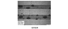
エッチレジストマスクを視覚的に検査した。図2Aに示されているように、印刷されたパターンは非常に悪い印刷品質を示し、ライン定義精度とライン切れが非常に悪くライン間の短絡状態が非常に悪いものであった。 The etch resist mask was visually inspected. As shown in FIG. 2A, the printed pattern showed very poor print quality, with very poor line definition accuracy and line breaks, and very poor short circuit between lines.
実施例2−液体組成物は実施例1に詳述したように調製した。FR4銅クラッド板表面を、銅クラッドを0.5%(w/w)のCuCl2水溶液に30秒間ディッピング(例えば、浸漬)して活性化させた後、工業用エタノールで銅ボードを洗浄した。 Example 2-The liquid composition was prepared as detailed in Example 1. The surface of the FR4 copper clad plate was activated by dipping (for example, immersing) the copper clad in a 0.5% (w / w) CuCl 2 aqueous solution for 30 seconds, and then the copper board was washed with industrial ethanol.
エプソン製stylus(登録商標)4900インクジェットプリンタを使用して、
処理した銅板の上に液体組成物を印刷し、80℃で乾燥させて不溶性エッチレジストマスクを製造した。エッチレジストパターンは、図2Bに示されているように、鋭いエッジを有し、ライン切れがなく、50μmまでの細い線幅を有し、明確に画定された薄いラインを有する高い印刷品質を示していた。露出した銅のエッチングおよびエッチレジストマスクの除去を、実施例1に詳述したように行った。板上の配線パターンは、鋭いエッジを有し、ライン切れがなく、50μmまでの細い線幅を有し、明確に画定された細いラインを示していた。
Using an Epson styles® 4900 inkjet printer,
The liquid composition was printed on the treated copper plate and dried at 80 ° C. to produce an insoluble etch resist mask. The etch resist pattern exhibits high print quality with sharp edges, no line breaks, fine line widths up to 50 μm, and well-defined thin lines, as shown in FIG. 2B. Was there. Etching of exposed copper and removal of the etch resist mask were performed as detailed in Example 1. The wiring pattern on the board showed sharp edges, no line breaks, narrow line widths up to 50 μm, and well-defined fine lines.
実施例3−液体組成物は実施例1に詳述したように調製した。銅表面を、20%(w/w)FeCl3水溶液を含有する槽に10秒間浸漬することによって活性化させた後、工業用エタノールで銅板を洗浄した。 Example 3-The liquid composition was prepared as detailed in Example 1. The copper surface was activated by immersing it in a bath containing a 20% (w / w) FeCl 3 aqueous solution for 10 seconds, and then the copper plate was washed with industrial ethanol.
実施例2と同様に、液体組成物をコーティングされた銅基板上にインクジェット印刷し、80℃で乾燥させて、不溶性エッチレジストマスクを生成した。エッチレジストパターンは、鋭いエッジを有し、ライン切れがなく、50μmまでの細い線幅を有し、明確に画定された細いラインを示していた。露出した銅のエッチングとエッチレジストマスクの除去は実施例1に詳述したように行った。板上の配線パターンは、鋭いエッジを有し、ライン切れがなく、30μmまでの細い線幅を有し、明確に画定された細いラインを示していた。 Similar to Example 2, the liquid composition was inkjet printed on a coated copper substrate and dried at 80 ° C. to produce an insoluble etch resist mask. The etch resist pattern had sharp edges, no line breaks, narrow line widths up to 50 μm, and showed well-defined fine lines. Etching of the exposed copper and removal of the etch resist mask were performed as detailed in Example 1. The wiring pattern on the board showed sharp edges, no line breaks, narrow line widths up to 30 μm, and well-defined fine lines.
実施例4−液体組成物は実施例1に詳述したように調製した。FR4銅クラッド板表面を、銅クラッドを1%(w/w)のNa2S2O8水溶液に30秒間浸漬して活性化させた後、工業用エタノールで銅ボードを洗浄した。 Example 4-The liquid composition was prepared as detailed in Example 1. The surface of the FR4 copper clad plate was activated by immersing the copper clad in a 1% (w / w) Na 2 S 2 O 8 aqueous solution for 30 seconds, and then the copper board was washed with industrial ethanol.
エプソン製stylus(登録商標)4900インクジェットプリンタを使用して、
処理した銅板の上に液体組成物を印刷し、80℃で乾燥させて不溶性エッチレジストマスクを製造した。エッチレジストパターンは、鋭いエッジを有し、ライン切れがなく、50μmまでの細い線幅を有し、明確に画定された薄いラインを有する高い印刷品質を示していた。露出した銅のエッチングおよびエッチレジストマスクの除去を、実施例1に詳述したように行った。板上の配線パターンは、鋭いエッジを有し、ライン切れがなく、30μmまでの細い線幅を有し、明確に画定された細いラインを示していた。
Using an Epson styles® 4900 inkjet printer,
The liquid composition was printed on the treated copper plate and dried at 80 ° C. to produce an insoluble etch resist mask. The etch resist pattern showed high print quality with sharp edges, no line breaks, fine line widths up to 50 μm, and well-defined thin lines. Etching of exposed copper and removal of the etch resist mask were performed as detailed in Example 1. The wiring pattern on the board showed sharp edges, no line breaks, narrow line widths up to 30 μm, and well-defined fine lines.
本発明の実施形態で使用される化学的表面活性化成分のいくつかの非限定的な例、および本発明のいくつかの実施形態による表面活性化溶液中のそれらの相対重量濃度並びに提示された浸漬時間を、以下の表1に列挙する。 Some non-limiting examples of chemical surface-activating components used in embodiments of the invention, and their relative weight concentrations in surface-activating solutions according to some embodiments of the invention, as well as presented. The soaking times are listed in Table 1 below.

エッチレジストインクのいくつかの非限定的な例を表2に列挙する。 Table 2 lists some non-limiting examples of etch resist inks.
本発明の特定の特徴を本明細書および図面において説明されてきたが、当業者であれば多くの改変態様、要素の置換および変更、および均等物を容易に想到されよう。従って、添付の特許請求の範囲は、本発明の精神の範囲に含まれる、あらゆるそのような修正および変更を含むことが意図されていることを理解されたい。
本発明は、例えば、以下を提供する:
(項目1)
基板上に金属パターンを形成する方法であって、
金属表面を化学的に活性化させる活性化剤を有する化学的表面活性化溶液を前記基板に結合された前記金属表面上に適用するステップと、
活性化された前記金属表面上にエッチレジストインクをノンインパクト印刷して、所定のパターンに従ってエッチレジストマスクを生成するステップであって、前記エッチレジストインク中の少なくとも1つのインク成分が、活性化された前記金属表面と化学反応を起こして前記エッチレジストインクの液滴を固定化する、該ステップと、
前記エッチレジストマスクで覆われていない非マスクの金属部分を除去するエッチングプロセスを行うステップと、
前記エッチレジストマスクを除去するステップとを含むことを特徴とする方法。
(項目2)
項目1に記載の方法であって、
前記金属パターンは、50μm未満の幅を有する金属線を含むことを特徴とする方法。
(項目3)
項目1に記載の方法であって、
前記エッチレジストマスクは、50μm未満の幅を有する線を含むことを特徴とする方法。
(項目4)
項目1に記載の方法であって、
前記金属パターンは、30μm未満の幅を有する金属線を含むことを特徴とする方法。
(項目5)
項目1に記載の方法であって、
前記エッチレジストマスクは、30μm未満の幅を有する線を含むことを特徴とする方法。
(項目6)
項目1に記載の方法であって、
印刷する前に、溶媒を用いて前記金属表面から前記化学的表面活性化溶液を除去するステップをさらに含むことを特徴とする方法。
(項目7)
項目1に記載の方法であって、
前記化学反応を起こす前記インク成分はアニオン成分であることを特徴とする方法。
(項目8)
項目1に記載の方法であって、
活性化された前記金属表面との化学反応を起こす前記インク成分は、アクリレート、ホスフェート、スルホネートまたはそれらの混合物から選択されるポリマー成分であることを特徴とする方法。
(項目9)
項目1に記載の方法であって、
前記活性化剤は、銅塩、第二鉄塩、クロム硫酸、過硫酸塩、亜塩素酸ナトリウムおよび過酸化水素の少なくとも1つまたはそれらの混合物を含むことを特徴とする方法。
(項目10)
項目1に記載の方法であって、
前記適用するステップは、約10〜60秒間、前記化学的表面活性化溶液を含む槽に前記金属表面を浸漬するステップを含むことを特徴とする方法。
(項目11)
項目1に記載の方法であって、
前記適用するステップは、前記化学的表面活性化溶液を前記金属表面の上にスプレーするステップを含むことを特徴とする方法。
(項目12)
項目1に記載の方法であって、
前記ノンインパクト印刷が、インクジェット印刷を含むことを特徴とする方法。
Although the particular features of the invention have been described herein and in the drawings, one of ordinary skill in the art will readily conceive of many modifications, element substitutions and modifications, and equivalents. Therefore, it should be understood that the appended claims are intended to include any such modifications and modifications that fall within the spirit of the invention.
The present invention provides, for example:
(Item 1)
A method of forming a metal pattern on a substrate,
A step of applying a chemical surface-activating solution having an activator that chemically activates the metal surface onto the metal surface bonded to the substrate.
A step of non-impact printing an etch resist ink on the activated metal surface to generate an etch resist mask according to a predetermined pattern, wherein at least one ink component in the etch resist ink is activated. The step of immobilizing the droplets of the etch resist ink by causing a chemical reaction with the metal surface.
A step of performing an etching process for removing a non-masked metal portion not covered by the etch resist mask,
A method comprising the step of removing the etch resist mask.
(Item 2)
The method described in item 1.
The method characterized in that the metal pattern contains a metal wire having a width of less than 50 μm.
(Item 3)
The method described in item 1.
The method characterized in that the etch resist mask contains a line having a width of less than 50 μm.
(Item 4)
The method described in item 1.
The method characterized in that the metal pattern contains a metal wire having a width of less than 30 μm.
(Item 5)
The method described in item 1.
The method characterized in that the etch resist mask contains a line having a width of less than 30 μm.
(Item 6)
The method described in item 1.
A method comprising further the step of removing the chemically surface-activating solution from the metal surface using a solvent prior to printing.
(Item 7)
The method described in item 1.
A method characterized in that the ink component that causes the chemical reaction is an anionic component.
(Item 8)
The method described in item 1.
A method characterized in that the ink component that causes a chemical reaction with the activated metal surface is a polymer component selected from acrylates, phosphates, sulfonates or mixtures thereof.
(Item 9)
The method described in item 1.
The method comprising the activator comprising at least one of copper salt, ferric salt, chromium sulfate, persulfate, sodium chlorite and hydrogen peroxide or a mixture thereof.
(Item 10)
The method described in item 1.
The applied step comprises immersing the metal surface in a bath containing the chemically surface-activating solution for about 10-60 seconds.
(Item 11)
The method described in item 1.
The method to be applied comprises the step of spraying the chemically surface-activating solution onto the metal surface.
(Item 12)
The method described in item 1.
A method characterized in that the non-impact printing includes inkjet printing.
Claims (12)
無機活性化剤を含む化学的表面活性化水溶液を、前記基板に結合された金属層の表面上に適用するステップであって、前記無機活性化剤は、前記金属層を化学的に活性化させて、前記金属層の表面に金属のイオンを形成するステップと、
前記金属層を化学的に活性化させた後に、前記金属層の表面上に反応性成分を含みかつ開始剤を含まないインクをノンインパクト印刷して、所定のパターンに従ってエッチレジストマスクを生成するステップであって、前記インクの液滴が前記金属層の表面に当たるときに、前記反応性成分が、前記金属層と化学反応を起こして前記インクの液滴を固定化するステップと、
前記金属層の、前記エッチレジストマスクで覆われていない部分を除去するエッチングプロセスを行うステップと、
前記エッチレジストマスクを除去して、前記金属パターンを形成するステップと、
を含むことを特徴とする方法。 A method of forming a metal pattern on a substrate,
A step of applying a chemical surface activating aqueous solution containing an inorganic activator onto the surface of a metal layer bonded to the substrate, wherein the inorganic activator chemically activates the metal layer. The step of forming metal ions on the surface of the metal layer,
After chemically activating the metal layer, an ink reactive components do not contain free Mikatsu initiator on the surface of the metal layer by non-impact printing, to produce an etch resist mask in accordance with a predetermined pattern A step in which, when the ink droplets hit the surface of the metal layer, the reactive component chemically reacts with the metal layer to immobilize the ink droplets.
A step of performing an etching process for removing a portion of the metal layer not covered by the etch resist mask,
The step of removing the etch resist mask to form the metal pattern,
A method characterized by including.
前記エッチングプロセスを行うステップによって形成される前記金属パターンは、50μm未満の幅を有する複数の金属線を含むことを特徴とする方法。 The method according to claim 1.
The method characterized in that the metal pattern formed by the step of performing the etching process contains a plurality of metal wires having a width of less than 50 μm.
前記ノンインパクト印刷から生成される前記エッチレジストマスクは、50μm未満の幅を有する複数の線を含むことを特徴とする方法。 The method according to claim 1.
A method characterized in that the etch resist mask produced from the non-impact printing contains a plurality of lines having a width of less than 50 μm.
前記エッチングプロセスを行うステップによって形成される前記金属パターンは、30μm未満の幅を有する複数の金属線を含むことを特徴とする方法。 The method according to claim 1.
A method characterized in that the metal pattern formed by the step of performing the etching process contains a plurality of metal wires having a width of less than 30 μm.
前記ノンインパクト印刷から生成される前記エッチレジストマスクは、30μm未満の幅を有する複数の線を含むことを特徴とする方法。 The method according to claim 1.
A method characterized in that the etch resist mask produced from the non-impact printing contains a plurality of lines having a width of less than 30 μm.
印刷する前に、溶媒を用いて、前記金属層の活性化された前記表面から前記化学的表面活性化水溶液を除去するステップをさらに含むことを特徴とする方法。 The method according to claim 1.
A method comprising the step of removing the chemically surface-activated aqueous solution from the activated surface of the metal layer using a solvent prior to printing.
前記金属層の活性化された前記表面との化学反応を起こす前記反応性成分は、アニオン成分であることを特徴とする方法。 The method according to claim 1.
A method characterized in that the reactive component that causes a chemical reaction with the activated surface of the metal layer is an anionic component.
前記金属層の活性化された前記表面との化学反応を起こす前記反応性成分は、アクリレート、ホスフェート、スルホネートまたはそれらの任意の組み合わせを含むポリマー成分であることを特徴とする方法。 The method according to claim 1.
A method characterized in that the reactive component that causes a chemical reaction with the activated surface of the metal layer is a polymer component comprising acrylate, phosphate, sulfonate or any combination thereof.
前記無機活性化剤は、銅塩、第二鉄塩、クロム硫酸、過硫酸塩、亜塩素酸ナトリウムおよび過酸化水素の少なくとも1つまたはそれらの混合物を含むことを特徴とする方法。 The method according to claim 1.
The method comprising the inorganic activator containing at least one of a copper salt, a ferric salt, a chromium sulfate, a persulfate, sodium chlorite and hydrogen peroxide, or a mixture thereof.
前記化学的表面活性化水溶液を適用するステップは、約10〜約60秒間、前記化学的表面活性化水溶液を含む槽に前記金属層の表面を浸漬するステップを含むことを特徴とする方法。 The method according to claim 1.
The step of applying the chemically surface-activated aqueous solution comprises immersing the surface of the metal layer in a tank containing the chemically surface-activated aqueous solution for about 10 to about 60 seconds.
前記化学的表面活性化水溶液を適用するステップは、前記化学的表面活性化水溶液を前記金属層の表面にスプレーするステップを含むことを特徴とする方法。 The method according to claim 1.
The method comprising applying the chemically surface-activated aqueous solution comprises spraying the chemically surface-activated aqueous solution onto the surface of the metal layer.
前記金属層の活性化された前記表面上に前記インクをノンインパクト印刷するステップが、インクジェット印刷を含むことを特徴とする方法。 The method according to claim 1.
A method characterized in that a step of non-impact printing the ink on the activated surface of the metal layer comprises inkjet printing.
Priority Applications (2)
| Application Number | Priority Date | Filing Date | Title |
|---|---|---|---|
| JP2021121139A JP7288644B2 (en) | 2015-08-13 | 2021-07-23 | Method for producing etch-resist patterns on metal surfaces |
| JP2023083553A JP2023116478A (en) | 2015-08-13 | 2023-05-21 | Production method of etching resist pattern on metal surface |
Applications Claiming Priority (3)
| Application Number | Priority Date | Filing Date | Title |
|---|---|---|---|
| US201562204508P | 2015-08-13 | 2015-08-13 | |
| US62/204,508 | 2015-08-13 | ||
| PCT/IL2016/050820 WO2017025949A1 (en) | 2015-08-13 | 2016-07-27 | Methods for producing an etch resist pattern on a metallic surface |
Related Child Applications (1)
| Application Number | Title | Priority Date | Filing Date |
|---|---|---|---|
| JP2021121139A Division JP7288644B2 (en) | 2015-08-13 | 2021-07-23 | Method for producing etch-resist patterns on metal surfaces |
Publications (3)
| Publication Number | Publication Date |
|---|---|
| JP2018527463A JP2018527463A (en) | 2018-09-20 |
| JP2018527463A5 JP2018527463A5 (en) | 2019-08-29 |
| JP6975463B2 true JP6975463B2 (en) | 2021-12-01 |
Family
ID=57983031
Family Applications (3)
| Application Number | Title | Priority Date | Filing Date |
|---|---|---|---|
| JP2018507595A Active JP6975463B2 (en) | 2015-08-13 | 2016-07-27 | Method for manufacturing etch resist pattern on metal surface |
| JP2021121139A Active JP7288644B2 (en) | 2015-08-13 | 2021-07-23 | Method for producing etch-resist patterns on metal surfaces |
| JP2023083553A Pending JP2023116478A (en) | 2015-08-13 | 2023-05-21 | Production method of etching resist pattern on metal surface |
Family Applications After (2)
| Application Number | Title | Priority Date | Filing Date |
|---|---|---|---|
| JP2021121139A Active JP7288644B2 (en) | 2015-08-13 | 2021-07-23 | Method for producing etch-resist patterns on metal surfaces |
| JP2023083553A Pending JP2023116478A (en) | 2015-08-13 | 2023-05-21 | Production method of etching resist pattern on metal surface |
Country Status (6)
| Country | Link |
|---|---|
| US (4) | US10806035B2 (en) |
| EP (2) | EP3866572B1 (en) |
| JP (3) | JP6975463B2 (en) |
| KR (3) | KR102508824B1 (en) |
| CN (2) | CN114397795A (en) |
| WO (1) | WO2017025949A1 (en) |
Families Citing this family (8)
| Publication number | Priority date | Publication date | Assignee | Title |
|---|---|---|---|---|
| CN113597123A (en) | 2015-06-04 | 2021-11-02 | 科迪华公司 | Method for producing etch-resistant patterns on metal surfaces and composition set thereof |
| KR102508824B1 (en) | 2015-08-13 | 2023-03-09 | 카티바, 인크. | Method of forming an etch resist pattern on a metal surface |
| US10398034B2 (en) | 2016-12-12 | 2019-08-27 | Kateeva, Inc. | Methods of etching conductive features, and related devices and systems |
| KR102460330B1 (en) * | 2017-10-23 | 2022-10-27 | 멕크 가부시키가이샤 | Method for producing a film-forming substrate, a film-forming substrate and a surface treatment agent |
| GB2583778B (en) * | 2019-03-29 | 2023-05-24 | Pierce Protocols Ltd | Glass etching preparation method and system |
| EP3985144A4 (en) * | 2019-06-11 | 2022-08-03 | Mitsubishi Gas Chemical Company, Inc. | Aqueous composition, method for roughening stainless steel surface in which same is used, roughened stainless steel, and method for manufacturing same |
| CN110468413A (en) * | 2019-09-10 | 2019-11-19 | 四会富仕电子科技股份有限公司 | A kind of method of Metal Substrate roughing in surface |
| US11826775B2 (en) * | 2022-03-07 | 2023-11-28 | CatMarks Manufacturing, LLC | Automotive part identification marking system |
Family Cites Families (69)
| Publication number | Priority date | Publication date | Assignee | Title |
|---|---|---|---|---|
| US4015706A (en) | 1971-11-15 | 1977-04-05 | Chemcut Corporation | Connecting modules for an etching system |
| US4127438A (en) * | 1977-11-07 | 1978-11-28 | International Business Machines Corporation | Adhesion promoter for additively plated printed circuit boards |
| DE3402883A1 (en) | 1984-01-27 | 1985-08-01 | Siemens AG, 1000 Berlin und 8000 München | Printed circuit boards made of laminated materials |
| EP0206030B1 (en) | 1985-06-07 | 1992-01-02 | Sekisui Kagaku Kogyo Kabushiki Kaisha | Photocurable composition |
| US4946711A (en) | 1987-10-14 | 1990-08-07 | Desoto, Inc. | Masking compositions and method for applying the same |
| JP2585070B2 (en) | 1988-08-02 | 1997-02-26 | 日本ペイント株式会社 | Image forming method |
| JPH06504628A (en) | 1990-12-20 | 1994-05-26 | エクソン・ケミカル・パテンツ・インク | UV/EB curable butyl copolymers for lithography and anti-corrosion coating applications |
| GB9425031D0 (en) | 1994-12-09 | 1995-02-08 | Alpha Metals Ltd | Printed circuit board manufacture |
| DE69635203T2 (en) | 1995-07-11 | 2006-06-29 | Delphi Technologies, Inc., Troy | Coatings and methods, in particular for printed circuit boards |
| EP0860742B1 (en) | 1997-02-25 | 2001-04-04 | E.I. Du Pont De Nemours And Company | Flexible, flame-retardant, photoimageable composition for coating printing circuits |
| US6222136B1 (en) | 1997-11-12 | 2001-04-24 | International Business Machines Corporation | Printed circuit board with continuous connective bumps |
| IL129307A0 (en) * | 1999-04-04 | 2000-02-17 | Scitex Corp Ltd | Process for direct digital printing of circuit boards |
| GB9916060D0 (en) | 1999-07-08 | 1999-09-08 | Isis Innovation | Printed circuit fabrication |
| JP3622910B2 (en) | 1999-07-30 | 2005-02-23 | セイコーエプソン株式会社 | Recording method for printing on recording medium using two liquids |
| US6399273B1 (en) | 1999-08-13 | 2002-06-04 | Board Of Regents, University Of Texas System | Water-processable photoresist compositions |
| JP4606684B2 (en) | 2000-03-29 | 2011-01-05 | 学校法人神奈川大学 | Photocurable / thermosetting resin composition, photosensitive dry film thereof and pattern forming method using the same |
| DE10066028C2 (en) * | 2000-07-07 | 2003-04-24 | Atotech Deutschland Gmbh | Copper substrate with roughened surfaces |
| JP3754303B2 (en) | 2001-02-16 | 2006-03-08 | 株式会社日立インフォメーションテクノロジー | SDRAM refresh circuit |
| JP2003012971A (en) | 2001-06-28 | 2003-01-15 | Konica Corp | Inkjet recording method |
| US7150816B2 (en) | 2001-08-31 | 2006-12-19 | Semitool, Inc. | Apparatus and method for deposition of an electrophoretic emulsion |
| US6709962B2 (en) * | 2002-03-19 | 2004-03-23 | N. Edward Berg | Process for manufacturing printed circuit boards |
| US20030177639A1 (en) * | 2002-03-19 | 2003-09-25 | Berg N. Edward | Process and apparatus for manufacturing printed circuit boards |
| SG107593A1 (en) * | 2002-06-04 | 2004-12-29 | Agency Science Tech & Res | Method for electroless metalisation of polymer substrate |
| GB0221891D0 (en) | 2002-09-20 | 2002-10-30 | Avecia Ltd | Process |
| TWI291726B (en) | 2002-10-25 | 2007-12-21 | Nanya Technology Corp | Process for etching metal layer |
| US7005241B2 (en) | 2003-06-09 | 2006-02-28 | Shinko Electric Industries Co., Ltd. | Process for making circuit board or lead frame |
| JP2005033049A (en) | 2003-07-08 | 2005-02-03 | Nec Toppan Circuit Solutions Inc | Wiring pattern formation method of printed wiring board and manufacturing method of printed wiring board |
| JP2005079479A (en) | 2003-09-02 | 2005-03-24 | Asahi Kasei Electronics Co Ltd | Resist ink for direct resist drawing |
| US7477627B2 (en) | 2003-09-10 | 2009-01-13 | Intel Corporation | Method and device of adaptive control of data rate, fragmentation and request to send protection in wireless networks |
| US20050067378A1 (en) * | 2003-09-30 | 2005-03-31 | Harry Fuerhaupter | Method for micro-roughening treatment of copper and mixed-metal circuitry |
| EP1678352A2 (en) | 2003-10-22 | 2006-07-12 | Nexx Systems, Inc. | Method and apparatus for fluid processing a workpiece |
| GB0324947D0 (en) | 2003-10-25 | 2003-11-26 | Avecia Ltd | Process |
| WO2005069705A1 (en) | 2004-01-15 | 2005-07-28 | Matsushita Electric Industrial Co., Ltd. | Metal pattern and process for producing the same |
| KR100828979B1 (en) | 2004-03-03 | 2008-05-14 | 이비덴 가부시키가이샤 | Etching solution, method of etching and printed wiring board |
| KR100585138B1 (en) | 2004-04-08 | 2006-05-30 | 삼성전자주식회사 | Mask pattern for manufacturing semiconductor device and method of forming the same and method of manufacturing semiconductor device having fine patterns |
| US20050250052A1 (en) | 2004-05-10 | 2005-11-10 | Nguyen Khe C | Maskless lithography using UV absorbing nano particle |
| GB0414840D0 (en) | 2004-07-02 | 2004-08-04 | Ncr Int Inc | Self-service terminal |
| KR100733920B1 (en) * | 2004-09-17 | 2007-07-02 | 주식회사 엘지화학 | Ink composition for etching resist, method of forming etching resist pattern and forming microchannel using the same |
| EP1937785A1 (en) | 2005-08-31 | 2008-07-02 | Printar Ltd. | Uv curable hybridcuring ink jet ink composition and solder mask using the same |
| KR100643934B1 (en) * | 2005-09-02 | 2006-11-10 | 삼성전기주식회사 | Method of forming circuit pattern of pcb |
| US7686986B2 (en) | 2006-01-05 | 2010-03-30 | Headwaters Technology Innovation, Llc | Magnesium hydroxide nanoparticles, methods of making same and compositions incorporating same |
| JP2007250884A (en) * | 2006-03-16 | 2007-09-27 | Shirai Denshi Kogyo Kk | Flexible printed circuit board and its manufacturing method |
| US20070237899A1 (en) * | 2006-04-05 | 2007-10-11 | David Sawoska | Process for creating a pattern on a copper surface |
| US20080308003A1 (en) | 2007-06-13 | 2008-12-18 | Krol Andrew M | UV inkjet resist |
| JP5454834B2 (en) | 2007-08-30 | 2014-03-26 | 日立化成株式会社 | Roughening device |
| JP2009158593A (en) | 2007-12-25 | 2009-07-16 | Tessera Interconnect Materials Inc | Bump structure and method of manufacturing the same |
| WO2009116401A1 (en) | 2008-03-17 | 2009-09-24 | 日立化成工業株式会社 | Photosensitive resin composition, and photosensitive element, solder resist and printed wiring board each using the composition |
| KR100986287B1 (en) | 2008-05-09 | 2010-10-07 | 삼성전기주식회사 | Ink-jet ejecting apparatus |
| WO2010086850A2 (en) * | 2009-01-29 | 2010-08-05 | Digiflex Ltd. | Process for producing a photomask on a photopolymeric surface |
| JP2011171323A (en) * | 2010-02-16 | 2011-09-01 | Mitsubishi Paper Mills Ltd | Etching method for copper or copper alloy |
| JP2011243256A (en) | 2010-05-19 | 2011-12-01 | Dainippon Printing Co Ltd | Suspension flexure substrate, suspension, suspension with head, and hard disk drive |
| WO2012067107A1 (en) | 2010-11-17 | 2012-05-24 | 日立化成工業株式会社 | Photosensitive resin composition, photosensitive element, method for forming resist pattern, and method for manufacturing printed wiring board |
| US20120288683A1 (en) | 2011-05-10 | 2012-11-15 | Chin-Te Kuo | Protuberant structure and method for making the same |
| WO2013004624A1 (en) * | 2011-07-07 | 2013-01-10 | Atotech Deutschland Gmbh | Method for providing organic resist adhesion to a copper or copper alloy surface |
| EP2748677A2 (en) * | 2011-08-24 | 2014-07-02 | Digiflex Ltd. | Process for dry-coating of flexographic surfaces |
| EP2753159B1 (en) | 2011-08-29 | 2018-12-19 | NGK Insulators, Ltd. | Laminated sintered ceramic wiring substrate, and semiconductor package containing wiring substrate |
| US9683305B2 (en) * | 2011-12-20 | 2017-06-20 | Apple Inc. | Metal surface and process for treating a metal surface |
| KR102026992B1 (en) | 2012-01-31 | 2019-09-30 | 아그파-게바에르트 엔.브이. | Radiation curable etch resistant inkjet ink printing |
| JP2013162007A (en) * | 2012-02-07 | 2013-08-19 | Toppan Printing Co Ltd | Production method of fine wiring pattern |
| US20140252571A1 (en) | 2013-03-06 | 2014-09-11 | Maxim Integrated Products, Inc. | Wafer-level package mitigated undercut |
| JP6164614B2 (en) | 2013-12-06 | 2017-07-19 | メック株式会社 | Etching solution, replenisher, and method for forming copper wiring |
| KR20230129193A (en) | 2013-12-06 | 2023-09-06 | 후지필름 일렉트로닉 머티리얼스 유.에스.에이., 아이엔씨. | Cleaning formulation for removing residues on surfaces |
| TWI500806B (en) | 2014-03-10 | 2015-09-21 | Nat Univ Tsing Hua | Method for manufacturing silicon carbide thin film |
| KR20150109932A (en) | 2014-03-21 | 2015-10-02 | 삼성전기주식회사 | Echtant and method for manufacturing circuit pattern using the same |
| US10498101B2 (en) | 2014-09-08 | 2019-12-03 | Kyushu University, National University Corporation | Method for producing organic microdisk structure |
| GB2538522B (en) | 2015-05-19 | 2019-03-06 | Dst Innovations Ltd | Electronic circuit and component construction |
| CN113597123A (en) | 2015-06-04 | 2021-11-02 | 科迪华公司 | Method for producing etch-resistant patterns on metal surfaces and composition set thereof |
| KR102508824B1 (en) | 2015-08-13 | 2023-03-09 | 카티바, 인크. | Method of forming an etch resist pattern on a metal surface |
| US10398034B2 (en) | 2016-12-12 | 2019-08-27 | Kateeva, Inc. | Methods of etching conductive features, and related devices and systems |
-
2016
- 2016-07-27 KR KR1020187007265A patent/KR102508824B1/en active IP Right Grant
- 2016-07-27 EP EP21166748.0A patent/EP3866572B1/en active Active
- 2016-07-27 CN CN202111517002.4A patent/CN114397795A/en active Pending
- 2016-07-27 CN CN201680048035.XA patent/CN108027553B/en active Active
- 2016-07-27 JP JP2018507595A patent/JP6975463B2/en active Active
- 2016-07-27 US US15/751,866 patent/US10806035B2/en active Active
- 2016-07-27 KR KR1020237007896A patent/KR102626521B1/en active IP Right Grant
- 2016-07-27 EP EP16834759.9A patent/EP3335079B1/en active Active
- 2016-07-27 WO PCT/IL2016/050820 patent/WO2017025949A1/en active Application Filing
- 2016-07-27 KR KR1020247001306A patent/KR20240014578A/en active Application Filing
-
2020
- 2020-09-24 US US16/948,597 patent/US11255018B2/en active Active
-
2021
- 2021-07-23 JP JP2021121139A patent/JP7288644B2/en active Active
-
2022
- 2022-01-12 US US17/647,756 patent/US11807947B2/en active Active
-
2023
- 2023-05-21 JP JP2023083553A patent/JP2023116478A/en active Pending
- 2023-10-10 US US18/483,673 patent/US20240035167A1/en active Pending
Also Published As
| Publication number | Publication date |
|---|---|
| KR20180074666A (en) | 2018-07-03 |
| JP2023116478A (en) | 2023-08-22 |
| JP2018527463A (en) | 2018-09-20 |
| EP3335079B1 (en) | 2021-05-12 |
| CN114397795A (en) | 2022-04-26 |
| US11255018B2 (en) | 2022-02-22 |
| KR20240014578A (en) | 2024-02-01 |
| CN108027553B (en) | 2021-12-31 |
| US20210007225A1 (en) | 2021-01-07 |
| WO2017025949A1 (en) | 2017-02-16 |
| JP2021192427A (en) | 2021-12-16 |
| JP7288644B2 (en) | 2023-06-08 |
| US11807947B2 (en) | 2023-11-07 |
| US20180242457A1 (en) | 2018-08-23 |
| EP3866572B1 (en) | 2024-01-03 |
| CN108027553A (en) | 2018-05-11 |
| EP3866572A3 (en) | 2021-09-29 |
| EP3866572A2 (en) | 2021-08-18 |
| US10806035B2 (en) | 2020-10-13 |
| EP3335079A4 (en) | 2019-03-27 |
| EP3335079A1 (en) | 2018-06-20 |
| US20240035167A1 (en) | 2024-02-01 |
| KR102626521B1 (en) | 2024-01-17 |
| KR20230036169A (en) | 2023-03-14 |
| KR102508824B1 (en) | 2023-03-09 |
| US20220136113A1 (en) | 2022-05-05 |
Similar Documents
| Publication | Publication Date | Title |
|---|---|---|
| JP6975463B2 (en) | Method for manufacturing etch resist pattern on metal surface | |
| JP7426735B2 (en) | Method for manufacturing etch resist patterns on metal surfaces | |
| JP2018527463A5 (en) | ||
| JP6325274B2 (en) | Polyimide resin surface modifier and polyimide resin surface modification method | |
| JP2023139049A (en) | Method of etching conductive feature, and related device and system | |
| TW201828358A (en) | Methods of etching conductive features, and related devices and systems |
Legal Events
| Date | Code | Title | Description |
|---|---|---|---|
| RD03 | Notification of appointment of power of attorney |
Free format text: JAPANESE INTERMEDIATE CODE: A7423 Effective date: 20180627 |
|
| RD04 | Notification of resignation of power of attorney |
Free format text: JAPANESE INTERMEDIATE CODE: A7424 Effective date: 20180628 |
|
| A521 | Request for written amendment filed |
Free format text: JAPANESE INTERMEDIATE CODE: A523 Effective date: 20190719 |
|
| A621 | Written request for application examination |
Free format text: JAPANESE INTERMEDIATE CODE: A621 Effective date: 20190719 |
|
| RD02 | Notification of acceptance of power of attorney |
Free format text: JAPANESE INTERMEDIATE CODE: A7422 Effective date: 20200703 |
|
| A977 | Report on retrieval |
Free format text: JAPANESE INTERMEDIATE CODE: A971007 Effective date: 20200717 |
|
| A131 | Notification of reasons for refusal |
Free format text: JAPANESE INTERMEDIATE CODE: A131 Effective date: 20200727 |
|
| RD04 | Notification of resignation of power of attorney |
Free format text: JAPANESE INTERMEDIATE CODE: A7424 Effective date: 20200825 |
|
| A601 | Written request for extension of time |
Free format text: JAPANESE INTERMEDIATE CODE: A601 Effective date: 20201027 |
|
| A521 | Request for written amendment filed |
Free format text: JAPANESE INTERMEDIATE CODE: A523 Effective date: 20201224 |
|
| A02 | Decision of refusal |
Free format text: JAPANESE INTERMEDIATE CODE: A02 Effective date: 20210326 |
|
| A521 | Request for written amendment filed |
Free format text: JAPANESE INTERMEDIATE CODE: A523 Effective date: 20210723 |
|
| C60 | Trial request (containing other claim documents, opposition documents) |
Free format text: JAPANESE INTERMEDIATE CODE: C60 Effective date: 20210723 |
|
| A911 | Transfer to examiner for re-examination before appeal (zenchi) |
Free format text: JAPANESE INTERMEDIATE CODE: A911 Effective date: 20210803 |
|
| C21 | Notice of transfer of a case for reconsideration by examiners before appeal proceedings |
Free format text: JAPANESE INTERMEDIATE CODE: C21 Effective date: 20210806 |
|
| TRDD | Decision of grant or rejection written | ||
| A01 | Written decision to grant a patent or to grant a registration (utility model) |
Free format text: JAPANESE INTERMEDIATE CODE: A01 Effective date: 20211001 |
|
| A61 | First payment of annual fees (during grant procedure) |
Free format text: JAPANESE INTERMEDIATE CODE: A61 Effective date: 20211029 |
|
| R150 | Certificate of patent or registration of utility model |
Ref document number: 6975463 Country of ref document: JP Free format text: JAPANESE INTERMEDIATE CODE: R150 |