JP6971952B2 - Semiconductor device - Google Patents
Semiconductor device Download PDFInfo
- Publication number
- JP6971952B2 JP6971952B2 JP2018209356A JP2018209356A JP6971952B2 JP 6971952 B2 JP6971952 B2 JP 6971952B2 JP 2018209356 A JP2018209356 A JP 2018209356A JP 2018209356 A JP2018209356 A JP 2018209356A JP 6971952 B2 JP6971952 B2 JP 6971952B2
- Authority
- JP
- Japan
- Prior art keywords
- resin
- uppermost
- contact
- wire
- semiconductor element
- Prior art date
- Legal status (The legal status is an assumption and is not a legal conclusion. Google has not performed a legal analysis and makes no representation as to the accuracy of the status listed.)
- Active
Links
Images


Classifications
-
- H—ELECTRICITY
- H01—ELECTRIC ELEMENTS
- H01L—SEMICONDUCTOR DEVICES NOT COVERED BY CLASS H10
- H01L24/00—Arrangements for connecting or disconnecting semiconductor or solid-state bodies; Methods or apparatus related thereto
- H01L24/01—Means for bonding being attached to, or being formed on, the surface to be connected, e.g. chip-to-package, die-attach, "first-level" interconnects; Manufacturing methods related thereto
- H01L24/42—Wire connectors; Manufacturing methods related thereto
- H01L24/47—Structure, shape, material or disposition of the wire connectors after the connecting process
- H01L24/49—Structure, shape, material or disposition of the wire connectors after the connecting process of a plurality of wire connectors
-
- H—ELECTRICITY
- H01—ELECTRIC ELEMENTS
- H01L—SEMICONDUCTOR DEVICES NOT COVERED BY CLASS H10
- H01L23/00—Details of semiconductor or other solid state devices
- H01L23/28—Encapsulations, e.g. encapsulating layers, coatings, e.g. for protection
- H01L23/29—Encapsulations, e.g. encapsulating layers, coatings, e.g. for protection characterised by the material, e.g. carbon
- H01L23/293—Organic, e.g. plastic
-
- H—ELECTRICITY
- H01—ELECTRIC ELEMENTS
- H01L—SEMICONDUCTOR DEVICES NOT COVERED BY CLASS H10
- H01L23/00—Details of semiconductor or other solid state devices
- H01L23/28—Encapsulations, e.g. encapsulating layers, coatings, e.g. for protection
- H01L23/31—Encapsulations, e.g. encapsulating layers, coatings, e.g. for protection characterised by the arrangement or shape
- H01L23/3107—Encapsulations, e.g. encapsulating layers, coatings, e.g. for protection characterised by the arrangement or shape the device being completely enclosed
- H01L23/3135—Double encapsulation or coating and encapsulation
-
- H—ELECTRICITY
- H01—ELECTRIC ELEMENTS
- H01L—SEMICONDUCTOR DEVICES NOT COVERED BY CLASS H10
- H01L23/00—Details of semiconductor or other solid state devices
- H01L23/48—Arrangements for conducting electric current to or from the solid state body in operation, e.g. leads, terminal arrangements ; Selection of materials therefor
- H01L23/488—Arrangements for conducting electric current to or from the solid state body in operation, e.g. leads, terminal arrangements ; Selection of materials therefor consisting of soldered or bonded constructions
- H01L23/495—Lead-frames or other flat leads
- H01L23/49517—Additional leads
- H01L23/4952—Additional leads the additional leads being a bump or a wire
-
- H—ELECTRICITY
- H01—ELECTRIC ELEMENTS
- H01L—SEMICONDUCTOR DEVICES NOT COVERED BY CLASS H10
- H01L23/00—Details of semiconductor or other solid state devices
- H01L23/48—Arrangements for conducting electric current to or from the solid state body in operation, e.g. leads, terminal arrangements ; Selection of materials therefor
- H01L23/488—Arrangements for conducting electric current to or from the solid state body in operation, e.g. leads, terminal arrangements ; Selection of materials therefor consisting of soldered or bonded constructions
- H01L23/495—Lead-frames or other flat leads
- H01L23/49541—Geometry of the lead-frame
- H01L23/49562—Geometry of the lead-frame for devices being provided for in H01L29/00
-
- H—ELECTRICITY
- H01—ELECTRIC ELEMENTS
- H01L—SEMICONDUCTOR DEVICES NOT COVERED BY CLASS H10
- H01L23/00—Details of semiconductor or other solid state devices
- H01L23/48—Arrangements for conducting electric current to or from the solid state body in operation, e.g. leads, terminal arrangements ; Selection of materials therefor
- H01L23/488—Arrangements for conducting electric current to or from the solid state body in operation, e.g. leads, terminal arrangements ; Selection of materials therefor consisting of soldered or bonded constructions
- H01L23/495—Lead-frames or other flat leads
- H01L23/49575—Assemblies of semiconductor devices on lead frames
-
- H—ELECTRICITY
- H01—ELECTRIC ELEMENTS
- H01L—SEMICONDUCTOR DEVICES NOT COVERED BY CLASS H10
- H01L23/00—Details of semiconductor or other solid state devices
- H01L23/52—Arrangements for conducting electric current within the device in operation from one component to another, i.e. interconnections, e.g. wires, lead frames
- H01L23/522—Arrangements for conducting electric current within the device in operation from one component to another, i.e. interconnections, e.g. wires, lead frames including external interconnections consisting of a multilayer structure of conductive and insulating layers inseparably formed on the semiconductor body
- H01L23/525—Arrangements for conducting electric current within the device in operation from one component to another, i.e. interconnections, e.g. wires, lead frames including external interconnections consisting of a multilayer structure of conductive and insulating layers inseparably formed on the semiconductor body with adaptable interconnections
- H01L23/5256—Arrangements for conducting electric current within the device in operation from one component to another, i.e. interconnections, e.g. wires, lead frames including external interconnections consisting of a multilayer structure of conductive and insulating layers inseparably formed on the semiconductor body with adaptable interconnections comprising fuses, i.e. connections having their state changed from conductive to non-conductive
-
- H—ELECTRICITY
- H01—ELECTRIC ELEMENTS
- H01L—SEMICONDUCTOR DEVICES NOT COVERED BY CLASS H10
- H01L23/00—Details of semiconductor or other solid state devices
- H01L23/58—Structural electrical arrangements for semiconductor devices not otherwise provided for, e.g. in combination with batteries
- H01L23/62—Protection against overvoltage, e.g. fuses, shunts
-
- H—ELECTRICITY
- H01—ELECTRIC ELEMENTS
- H01L—SEMICONDUCTOR DEVICES NOT COVERED BY CLASS H10
- H01L24/00—Arrangements for connecting or disconnecting semiconductor or solid-state bodies; Methods or apparatus related thereto
- H01L24/01—Means for bonding being attached to, or being formed on, the surface to be connected, e.g. chip-to-package, die-attach, "first-level" interconnects; Manufacturing methods related thereto
- H01L24/42—Wire connectors; Manufacturing methods related thereto
- H01L24/47—Structure, shape, material or disposition of the wire connectors after the connecting process
- H01L24/48—Structure, shape, material or disposition of the wire connectors after the connecting process of an individual wire connector
-
- H—ELECTRICITY
- H01—ELECTRIC ELEMENTS
- H01L—SEMICONDUCTOR DEVICES NOT COVERED BY CLASS H10
- H01L25/00—Assemblies consisting of a plurality of individual semiconductor or other solid state devices ; Multistep manufacturing processes thereof
- H01L25/03—Assemblies consisting of a plurality of individual semiconductor or other solid state devices ; Multistep manufacturing processes thereof all the devices being of a type provided for in the same subgroup of groups H01L27/00 - H01L33/00, or in a single subclass of H10K, H10N, e.g. assemblies of rectifier diodes
- H01L25/04—Assemblies consisting of a plurality of individual semiconductor or other solid state devices ; Multistep manufacturing processes thereof all the devices being of a type provided for in the same subgroup of groups H01L27/00 - H01L33/00, or in a single subclass of H10K, H10N, e.g. assemblies of rectifier diodes the devices not having separate containers
- H01L25/07—Assemblies consisting of a plurality of individual semiconductor or other solid state devices ; Multistep manufacturing processes thereof all the devices being of a type provided for in the same subgroup of groups H01L27/00 - H01L33/00, or in a single subclass of H10K, H10N, e.g. assemblies of rectifier diodes the devices not having separate containers the devices being of a type provided for in group H01L29/00
- H01L25/071—Assemblies consisting of a plurality of individual semiconductor or other solid state devices ; Multistep manufacturing processes thereof all the devices being of a type provided for in the same subgroup of groups H01L27/00 - H01L33/00, or in a single subclass of H10K, H10N, e.g. assemblies of rectifier diodes the devices not having separate containers the devices being of a type provided for in group H01L29/00 the devices being arranged next and on each other, i.e. mixed assemblies
-
- H—ELECTRICITY
- H01—ELECTRIC ELEMENTS
- H01L—SEMICONDUCTOR DEVICES NOT COVERED BY CLASS H10
- H01L25/00—Assemblies consisting of a plurality of individual semiconductor or other solid state devices ; Multistep manufacturing processes thereof
- H01L25/03—Assemblies consisting of a plurality of individual semiconductor or other solid state devices ; Multistep manufacturing processes thereof all the devices being of a type provided for in the same subgroup of groups H01L27/00 - H01L33/00, or in a single subclass of H10K, H10N, e.g. assemblies of rectifier diodes
- H01L25/04—Assemblies consisting of a plurality of individual semiconductor or other solid state devices ; Multistep manufacturing processes thereof all the devices being of a type provided for in the same subgroup of groups H01L27/00 - H01L33/00, or in a single subclass of H10K, H10N, e.g. assemblies of rectifier diodes the devices not having separate containers
- H01L25/07—Assemblies consisting of a plurality of individual semiconductor or other solid state devices ; Multistep manufacturing processes thereof all the devices being of a type provided for in the same subgroup of groups H01L27/00 - H01L33/00, or in a single subclass of H10K, H10N, e.g. assemblies of rectifier diodes the devices not having separate containers the devices being of a type provided for in group H01L29/00
- H01L25/072—Assemblies consisting of a plurality of individual semiconductor or other solid state devices ; Multistep manufacturing processes thereof all the devices being of a type provided for in the same subgroup of groups H01L27/00 - H01L33/00, or in a single subclass of H10K, H10N, e.g. assemblies of rectifier diodes the devices not having separate containers the devices being of a type provided for in group H01L29/00 the devices being arranged next to each other
-
- H—ELECTRICITY
- H01—ELECTRIC ELEMENTS
- H01L—SEMICONDUCTOR DEVICES NOT COVERED BY CLASS H10
- H01L25/00—Assemblies consisting of a plurality of individual semiconductor or other solid state devices ; Multistep manufacturing processes thereof
- H01L25/18—Assemblies consisting of a plurality of individual semiconductor or other solid state devices ; Multistep manufacturing processes thereof the devices being of types provided for in two or more different subgroups of the same main group of groups H01L27/00 - H01L33/00, or in a single subclass of H10K, H10N
-
- H—ELECTRICITY
- H01—ELECTRIC ELEMENTS
- H01L—SEMICONDUCTOR DEVICES NOT COVERED BY CLASS H10
- H01L2224/00—Indexing scheme for arrangements for connecting or disconnecting semiconductor or solid-state bodies and methods related thereto as covered by H01L24/00
- H01L2224/01—Means for bonding being attached to, or being formed on, the surface to be connected, e.g. chip-to-package, die-attach, "first-level" interconnects; Manufacturing methods related thereto
- H01L2224/02—Bonding areas; Manufacturing methods related thereto
- H01L2224/04—Structure, shape, material or disposition of the bonding areas prior to the connecting process
- H01L2224/04042—Bonding areas specifically adapted for wire connectors, e.g. wirebond pads
-
- H—ELECTRICITY
- H01—ELECTRIC ELEMENTS
- H01L—SEMICONDUCTOR DEVICES NOT COVERED BY CLASS H10
- H01L2224/00—Indexing scheme for arrangements for connecting or disconnecting semiconductor or solid-state bodies and methods related thereto as covered by H01L24/00
- H01L2224/01—Means for bonding being attached to, or being formed on, the surface to be connected, e.g. chip-to-package, die-attach, "first-level" interconnects; Manufacturing methods related thereto
- H01L2224/02—Bonding areas; Manufacturing methods related thereto
- H01L2224/04—Structure, shape, material or disposition of the bonding areas prior to the connecting process
- H01L2224/06—Structure, shape, material or disposition of the bonding areas prior to the connecting process of a plurality of bonding areas
- H01L2224/0601—Structure
- H01L2224/0603—Bonding areas having different sizes, e.g. different heights or widths
-
- H—ELECTRICITY
- H01—ELECTRIC ELEMENTS
- H01L—SEMICONDUCTOR DEVICES NOT COVERED BY CLASS H10
- H01L2224/00—Indexing scheme for arrangements for connecting or disconnecting semiconductor or solid-state bodies and methods related thereto as covered by H01L24/00
- H01L2224/01—Means for bonding being attached to, or being formed on, the surface to be connected, e.g. chip-to-package, die-attach, "first-level" interconnects; Manufacturing methods related thereto
- H01L2224/26—Layer connectors, e.g. plate connectors, solder or adhesive layers; Manufacturing methods related thereto
- H01L2224/31—Structure, shape, material or disposition of the layer connectors after the connecting process
- H01L2224/32—Structure, shape, material or disposition of the layer connectors after the connecting process of an individual layer connector
- H01L2224/321—Disposition
- H01L2224/32151—Disposition the layer connector connecting between a semiconductor or solid-state body and an item not being a semiconductor or solid-state body, e.g. chip-to-substrate, chip-to-passive
- H01L2224/32221—Disposition the layer connector connecting between a semiconductor or solid-state body and an item not being a semiconductor or solid-state body, e.g. chip-to-substrate, chip-to-passive the body and the item being stacked
- H01L2224/32245—Disposition the layer connector connecting between a semiconductor or solid-state body and an item not being a semiconductor or solid-state body, e.g. chip-to-substrate, chip-to-passive the body and the item being stacked the item being metallic
-
- H—ELECTRICITY
- H01—ELECTRIC ELEMENTS
- H01L—SEMICONDUCTOR DEVICES NOT COVERED BY CLASS H10
- H01L2224/00—Indexing scheme for arrangements for connecting or disconnecting semiconductor or solid-state bodies and methods related thereto as covered by H01L24/00
- H01L2224/01—Means for bonding being attached to, or being formed on, the surface to be connected, e.g. chip-to-package, die-attach, "first-level" interconnects; Manufacturing methods related thereto
- H01L2224/42—Wire connectors; Manufacturing methods related thereto
- H01L2224/47—Structure, shape, material or disposition of the wire connectors after the connecting process
- H01L2224/48—Structure, shape, material or disposition of the wire connectors after the connecting process of an individual wire connector
- H01L2224/481—Disposition
- H01L2224/48135—Connecting between different semiconductor or solid-state bodies, i.e. chip-to-chip
- H01L2224/48137—Connecting between different semiconductor or solid-state bodies, i.e. chip-to-chip the bodies being arranged next to each other, e.g. on a common substrate
- H01L2224/48139—Connecting between different semiconductor or solid-state bodies, i.e. chip-to-chip the bodies being arranged next to each other, e.g. on a common substrate with an intermediate bond, e.g. continuous wire daisy chain
-
- H—ELECTRICITY
- H01—ELECTRIC ELEMENTS
- H01L—SEMICONDUCTOR DEVICES NOT COVERED BY CLASS H10
- H01L2224/00—Indexing scheme for arrangements for connecting or disconnecting semiconductor or solid-state bodies and methods related thereto as covered by H01L24/00
- H01L2224/01—Means for bonding being attached to, or being formed on, the surface to be connected, e.g. chip-to-package, die-attach, "first-level" interconnects; Manufacturing methods related thereto
- H01L2224/42—Wire connectors; Manufacturing methods related thereto
- H01L2224/47—Structure, shape, material or disposition of the wire connectors after the connecting process
- H01L2224/48—Structure, shape, material or disposition of the wire connectors after the connecting process of an individual wire connector
- H01L2224/481—Disposition
- H01L2224/48151—Connecting between a semiconductor or solid-state body and an item not being a semiconductor or solid-state body, e.g. chip-to-substrate, chip-to-passive
- H01L2224/48221—Connecting between a semiconductor or solid-state body and an item not being a semiconductor or solid-state body, e.g. chip-to-substrate, chip-to-passive the body and the item being stacked
- H01L2224/48245—Connecting between a semiconductor or solid-state body and an item not being a semiconductor or solid-state body, e.g. chip-to-substrate, chip-to-passive the body and the item being stacked the item being metallic
- H01L2224/48247—Connecting between a semiconductor or solid-state body and an item not being a semiconductor or solid-state body, e.g. chip-to-substrate, chip-to-passive the body and the item being stacked the item being metallic connecting the wire to a bond pad of the item
-
- H—ELECTRICITY
- H01—ELECTRIC ELEMENTS
- H01L—SEMICONDUCTOR DEVICES NOT COVERED BY CLASS H10
- H01L2224/00—Indexing scheme for arrangements for connecting or disconnecting semiconductor or solid-state bodies and methods related thereto as covered by H01L24/00
- H01L2224/01—Means for bonding being attached to, or being formed on, the surface to be connected, e.g. chip-to-package, die-attach, "first-level" interconnects; Manufacturing methods related thereto
- H01L2224/42—Wire connectors; Manufacturing methods related thereto
- H01L2224/47—Structure, shape, material or disposition of the wire connectors after the connecting process
- H01L2224/49—Structure, shape, material or disposition of the wire connectors after the connecting process of a plurality of wire connectors
- H01L2224/4901—Structure
- H01L2224/4903—Connectors having different sizes, e.g. different diameters
-
- H—ELECTRICITY
- H01—ELECTRIC ELEMENTS
- H01L—SEMICONDUCTOR DEVICES NOT COVERED BY CLASS H10
- H01L2224/00—Indexing scheme for arrangements for connecting or disconnecting semiconductor or solid-state bodies and methods related thereto as covered by H01L24/00
- H01L2224/01—Means for bonding being attached to, or being formed on, the surface to be connected, e.g. chip-to-package, die-attach, "first-level" interconnects; Manufacturing methods related thereto
- H01L2224/42—Wire connectors; Manufacturing methods related thereto
- H01L2224/47—Structure, shape, material or disposition of the wire connectors after the connecting process
- H01L2224/49—Structure, shape, material or disposition of the wire connectors after the connecting process of a plurality of wire connectors
- H01L2224/4905—Shape
- H01L2224/49051—Connectors having different shapes
-
- H—ELECTRICITY
- H01—ELECTRIC ELEMENTS
- H01L—SEMICONDUCTOR DEVICES NOT COVERED BY CLASS H10
- H01L2224/00—Indexing scheme for arrangements for connecting or disconnecting semiconductor or solid-state bodies and methods related thereto as covered by H01L24/00
- H01L2224/73—Means for bonding being of different types provided for in two or more of groups H01L2224/10, H01L2224/18, H01L2224/26, H01L2224/34, H01L2224/42, H01L2224/50, H01L2224/63, H01L2224/71
- H01L2224/732—Location after the connecting process
- H01L2224/73251—Location after the connecting process on different surfaces
- H01L2224/73265—Layer and wire connectors
-
- H—ELECTRICITY
- H01—ELECTRIC ELEMENTS
- H01L—SEMICONDUCTOR DEVICES NOT COVERED BY CLASS H10
- H01L2224/00—Indexing scheme for arrangements for connecting or disconnecting semiconductor or solid-state bodies and methods related thereto as covered by H01L24/00
- H01L2224/80—Methods for connecting semiconductor or other solid state bodies using means for bonding being attached to, or being formed on, the surface to be connected
- H01L2224/85—Methods for connecting semiconductor or other solid state bodies using means for bonding being attached to, or being formed on, the surface to be connected using a wire connector
- H01L2224/85909—Post-treatment of the connector or wire bonding area
- H01L2224/8592—Applying permanent coating, e.g. protective coating
-
- H—ELECTRICITY
- H01—ELECTRIC ELEMENTS
- H01L—SEMICONDUCTOR DEVICES NOT COVERED BY CLASS H10
- H01L23/00—Details of semiconductor or other solid state devices
- H01L23/34—Arrangements for cooling, heating, ventilating or temperature compensation ; Temperature sensing arrangements
- H01L23/36—Selection of materials, or shaping, to facilitate cooling or heating, e.g. heatsinks
- H01L23/373—Cooling facilitated by selection of materials for the device or materials for thermal expansion adaptation, e.g. carbon
- H01L23/3737—Organic materials with or without a thermoconductive filler
-
- H—ELECTRICITY
- H01—ELECTRIC ELEMENTS
- H01L—SEMICONDUCTOR DEVICES NOT COVERED BY CLASS H10
- H01L24/00—Arrangements for connecting or disconnecting semiconductor or solid-state bodies; Methods or apparatus related thereto
- H01L24/01—Means for bonding being attached to, or being formed on, the surface to be connected, e.g. chip-to-package, die-attach, "first-level" interconnects; Manufacturing methods related thereto
- H01L24/26—Layer connectors, e.g. plate connectors, solder or adhesive layers; Manufacturing methods related thereto
- H01L24/31—Structure, shape, material or disposition of the layer connectors after the connecting process
- H01L24/32—Structure, shape, material or disposition of the layer connectors after the connecting process of an individual layer connector
-
- H—ELECTRICITY
- H01—ELECTRIC ELEMENTS
- H01L—SEMICONDUCTOR DEVICES NOT COVERED BY CLASS H10
- H01L24/00—Arrangements for connecting or disconnecting semiconductor or solid-state bodies; Methods or apparatus related thereto
- H01L24/73—Means for bonding being of different types provided for in two or more of groups H01L24/10, H01L24/18, H01L24/26, H01L24/34, H01L24/42, H01L24/50, H01L24/63, H01L24/71
-
- H—ELECTRICITY
- H01—ELECTRIC ELEMENTS
- H01L—SEMICONDUCTOR DEVICES NOT COVERED BY CLASS H10
- H01L2924/00—Indexing scheme for arrangements or methods for connecting or disconnecting semiconductor or solid-state bodies as covered by H01L24/00
- H01L2924/15—Details of package parts other than the semiconductor or other solid state devices to be connected
- H01L2924/181—Encapsulation
- H01L2924/1815—Shape
Description
本発明は、複数のワイヤにより複数の半導体素子が接続された構成を有する半導体装置に関する。 The present invention relates to a semiconductor device having a configuration in which a plurality of semiconductor elements are connected by a plurality of wires.
電力用半導体装置等の半導体装置には、複数の半導体素子が設けられている。当該複数の半導体素子に含まれる隣接する2つの半導体素子は、例えば、複数のワイヤにより接続されている場合もある。なお、半導体装置では、様々な要因により、当該複数のワイヤに過電流が流れる場合がある。当該様々な要因は、例えば、短絡箇所の発生、静電気の発生等である。以下においては、隣接する2つの半導体素子を接続する複数のワイヤに過電流が流れる状況を、「過電流状況」ともいう。 A plurality of semiconductor elements are provided in a semiconductor device such as a power semiconductor device. Two adjacent semiconductor elements included in the plurality of semiconductor elements may be connected by, for example, a plurality of wires. In a semiconductor device, an overcurrent may flow through the plurality of wires due to various factors. The various factors are, for example, the generation of short-circuited portions, the generation of static electricity, and the like. In the following, a situation in which an overcurrent flows through a plurality of wires connecting two adjacent semiconductor elements is also referred to as an “overcurrent situation”.
過電流状況では、複数のワイヤが接続されている、当該2つの半導体素子の両方または一方が故障する可能性がある。このような事態の発生を抑制するために、半導体装置におけるワイヤをヒューズとして利用する技術が使用される。 In an overcurrent situation, both or one of the two semiconductor devices to which the plurality of wires are connected can fail. In order to suppress the occurrence of such a situation, a technique of using a wire as a fuse in a semiconductor device is used.
特許文献1では、ワイヤをヒューズとして利用する技術を使用した構成(以下、「関連構成A」ともいう)が開示されている。 Patent Document 1 discloses a configuration using a technique of using a wire as a fuse (hereinafter, also referred to as “related configuration A”).
隣接する2つの半導体素子が複数のワイヤにより接続されている構成を有する半導体装置がある。なお、過電流状況において、当該複数のワイヤが過電流により溶断されない可能性がある。当該複数のワイヤが過電流により溶断されない場合、当該過電流により、当該半導体素子が故障する可能性があるという問題がある。 There is a semiconductor device having a configuration in which two adjacent semiconductor elements are connected by a plurality of wires. In an overcurrent situation, the plurality of wires may not be blown due to the overcurrent. If the plurality of wires are not blown by the overcurrent, there is a problem that the semiconductor element may fail due to the overcurrent.
本発明は、このような問題を解決するためになされたものであり、ワイヤに過電流が流れる状況において、当該ワイヤが溶断されやすい半導体装置を提供することを目的とする。 The present invention has been made to solve such a problem, and an object of the present invention is to provide a semiconductor device in which the wire is easily blown in a situation where an overcurrent flows through the wire.
上記目的を達成するために、本発明の一態様に係る半導体装置は、第1半導体素子と、平面視において、前記第1半導体素子に隣接している第2半導体素子と、を備える。前記第1半導体素子は、第1ワイヤおよび第2ワイヤにより、前記第2半導体素子に接続されており、前記第1ワイヤは、前記第1半導体素子に接続されている第1接点と、前記第2半導体素子に接続されている第2接点とを有し、前記第2ワイヤは、前記第1半導体素子に接続されている第3接点と、前記第2半導体素子に接続されている第4接点とを有し、前記第1ワイヤのうち前記第1接点と前記第2接点との間の部分である第1線状部は、起伏を有し、前記第2ワイヤのうち前記第3接点と前記第4接点との間の部分である第2線状部は、起伏を有し、前記第1線状部の第1最上部は、前記第2線状部の第2最上部に隣接しており、前記第1最上部と前記第2最上部との間隔は、前記第1接点と前記第3接点との間隔より狭く、前記第1最上部と前記第2最上部との間隔は、前記第2接点と前記第4接点との間隔より狭い。 In order to achieve the above object, the semiconductor device according to one aspect of the present invention includes a first semiconductor element and a second semiconductor element adjacent to the first semiconductor element in a plan view. The first semiconductor element is connected to the second semiconductor element by a first wire and a second wire, and the first wire is a first contact connected to the first semiconductor element and the first. The second contact has a second contact connected to the two semiconductor elements, and the second wire has a third contact connected to the first semiconductor element and a fourth contact connected to the second semiconductor element. The first linear portion, which is a portion of the first wire between the first contact and the second contact, has undulations and has undulations with the third contact of the second wire. The second linear portion, which is a portion between the fourth contact point, has undulations, and the first uppermost portion of the first linear portion is adjacent to the second uppermost portion of the second linear portion. The distance between the first uppermost part and the second uppermost part is narrower than the distance between the first contact point and the third contact point, and the distance between the first uppermost part and the second uppermost part is set. It is narrower than the distance between the second contact and the fourth contact.
本発明によれば、前記第1ワイヤは、前記第1半導体素子に接続されている第1接点と、前記第2半導体素子に接続されている第2接点とを有する。前記第2ワイヤは、前記第1半導体素子に接続されている第3接点と、前記第2半導体素子に接続されている第4接点とを有する。 According to the present invention, the first wire has a first contact connected to the first semiconductor element and a second contact connected to the second semiconductor element. The second wire has a third contact connected to the first semiconductor element and a fourth contact connected to the second semiconductor element.
前記第1ワイヤのうち前記第1接点と前記第2接点との間の部分である第1線状部は、起伏を有する。前記第2ワイヤのうち前記第3接点と前記第4接点との間の部分である第2線状部は、起伏を有する。 The first linear portion of the first wire, which is a portion between the first contact and the second contact, has undulations. The second linear portion of the second wire, which is a portion between the third contact and the fourth contact, has undulations.
前記第1線状部の第1最上部は、前記第2線状部の第2最上部に隣接している。前記第1最上部と前記第2最上部との間隔は、前記第1接点と前記第3接点との間隔より狭い。前記第1最上部と前記第2最上部との間隔は、前記第2接点と前記第4接点との間隔より狭い。 The first uppermost portion of the first linear portion is adjacent to the second uppermost portion of the second linear portion. The distance between the first uppermost part and the second uppermost part is narrower than the distance between the first contact point and the third contact point. The distance between the first uppermost portion and the second uppermost portion is narrower than the distance between the second contact point and the fourth contact point.
これにより、ワイヤに過電流が流れる状況において、前記第1最上部および前記第2最上部の温度は、前記第1接点および前記第3接点の温度よりも、高くなる。そのため、前記第1ワイヤの一部である第1最上部、および、前記第2ワイヤの一部である第2最上部が、過電流により溶断されやすくなる。すなわち、ワイヤに過電流が流れる状況において、当該ワイヤが溶断されやすい半導体装置を提供することができる。 As a result, in a situation where an overcurrent flows through the wire, the temperature of the first uppermost portion and the second uppermost portion becomes higher than the temperature of the first contact and the third contact. Therefore, the first uppermost portion, which is a part of the first wire, and the second uppermost portion, which is a part of the second wire, are easily blown by the overcurrent. That is, it is possible to provide a semiconductor device in which the wire is easily blown in a situation where an overcurrent flows through the wire.
以下、図面を参照しつつ、実施の形態について説明する。以下の図面では、同一の各構成要素には同一の符号を付してある。同一の符号が付されている各構成要素の名称および機能は同じである。したがって、同一の符号が付されている各構成要素の一部についての詳細な説明を省略する場合がある。 Hereinafter, embodiments will be described with reference to the drawings. In the drawings below, the same components are designated by the same reference numerals. The names and functions of the components with the same reference numerals are the same. Therefore, detailed description of some of the components with the same reference numerals may be omitted.
なお、実施の形態において例示される各構成要素の寸法、材質、形状、当該各構成要素の相対配置などは、装置の構成、各種条件等により適宜変更されてもよい。また、各図における各構成要素の寸法は、実際の寸法と異なる場合がある。 The dimensions, materials, shapes, relative arrangements, and the like of each component exemplified in the embodiment may be appropriately changed depending on the configuration of the device, various conditions, and the like. In addition, the dimensions of each component in each figure may differ from the actual dimensions.
<実施の形態1>
図1は、実施の形態1に係る半導体装置100の側面図である。半導体装置100は、例えば、電力用半導体装置である。図1において、X方向、Y方向およびZ方向は、互いに直交する。以下の図に示されるX方向、Y方向およびZ方向も、互いに直交する。以下においては、X方向と、当該X方向の反対の方向(−X方向)とを含む方向を「X軸方向」ともいう。また、以下においては、Y方向と、当該Y方向の反対の方向(−Y方向)とを含む方向を「Y軸方向」ともいう。また、以下においては、Z方向と、当該Z方向の反対の方向(−Z方向)とを含む方向を「Z軸方向」ともいう。
<Embodiment 1>
FIG. 1 is a side view of the
また、以下においては、X軸方向およびY軸方向を含む平面を、「XY面」ともいう。また、以下においては、X軸方向およびZ軸方向を含む平面を、「XZ面」ともいう。また、以下においては、Y軸方向およびZ軸方向を含む平面を、「YZ面」ともいう。 Further, in the following, a plane including the X-axis direction and the Y-axis direction is also referred to as an “XY plane”. Further, in the following, a plane including the X-axis direction and the Z-axis direction is also referred to as an “XZ plane”. Further, in the following, a plane including the Y-axis direction and the Z-axis direction is also referred to as a “YZ plane”.
図1を参照して、半導体装置100は、パッケージP1を備える。パッケージP1は、上面P1sを有する。パッケージP1は、樹脂R1で構成されている。すなわち、半導体装置100は、樹脂R1を備える。
With reference to FIG. 1, the
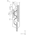
図2は、実施の形態1に係る半導体装置100の一部を示す平面図である。なお、図2は、パッケージP1の内部構成を示している。また、図2では、半導体装置100における1つのアーム部が示されている。図3は、図2のA1−A2間の一点鎖線に沿った、半導体装置100の断面図である。
FIG. 2 is a plan view showing a part of the
図2および図3を参照して、半導体装置100は、さらに、リードフレームF1,F2と、半導体素子S1aと、半導体素子S1bと、複数のワイヤW1とを備える。
With reference to FIGS. 2 and 3, the
リードフレームF1,F2の各々の形状は、板状である。リードフレームF1,F2の各々は、金属で構成される。リードフレームF1,F2の各々は、配線状に加工された、板状の金属である。 Each of the lead frames F1 and F2 has a plate shape. Each of the lead frames F1 and F2 is made of metal. Each of the lead frames F1 and F2 is a plate-shaped metal processed into a wiring shape.
リードフレームF1には、半導体素子S1a,S1bが実装されている。平面視(XY面)において、半導体素子S1bは、半導体素子S1aに隣接している。半導体素子S1aは、例えば、スイッチング素子としてのIGBT(Insulated Gate Bipolar Transistor)である。IGBTは、主電流の流れを制御する機能を有する。半導体素子S1bは、例えば、還流ダイオード(Free Wheeling Diode)である。還流ダイオードは、IGBTがオフ状態であるときに還流電流を流す機能を有する。 Semiconductor elements S1a and S1b are mounted on the lead frame F1. In a plan view (XY plane), the semiconductor element S1b is adjacent to the semiconductor element S1a. The semiconductor element S1a is, for example, an IGBT (Insulated Gate Bipolar Transistor) as a switching element. The IGBT has a function of controlling the flow of the main current. The semiconductor element S1b is, for example, a free wheeling diode. The freewheeling diode has a function of passing a freewheeling current when the IGBT is in the off state.
半導体素子S1aおよび半導体素子S1bは、詳細は後述するが、複数のワイヤW1およびリードフレームF1により、電気的に逆並列に接続されている。 Although the details of the semiconductor element S1a and the semiconductor element S1b will be described later, the semiconductor element S1a and the semiconductor element S1b are electrically connected in antiparallel by a plurality of wires W1 and a lead frame F1.
半導体素子S1aの上面には、電極E1aが設けられている。電極E1aは、エミッタ電極である。半導体素子S1aの底面には、コレクタ電極(図示せず)が設けられている。半導体素子S1aのコレクタ電極(図示せず)は、リードフレームF1に接続される。リードフレームF1は、IGBTのコレクタ側の外部接続端子(コレクタ側端子)として機能する。 An electrode E1a is provided on the upper surface of the semiconductor element S1a. The electrode E1a is an emitter electrode. A collector electrode (not shown) is provided on the bottom surface of the semiconductor element S1a. The collector electrode (not shown) of the semiconductor element S1a is connected to the lead frame F1. The lead frame F1 functions as an external connection terminal (collector side terminal) on the collector side of the IGBT.
半導体素子S1bの上面には、電極E1bが設けられている。電極E1bは、アノード電極である。半導体素子S1bの底面には、カソード電極(図示せず)が設けられている。半導体素子S1bのカソード電極(図示せず)は、リードフレームF1に接続される。 An electrode E1b is provided on the upper surface of the semiconductor element S1b. The electrode E1b is an anode electrode. A cathode electrode (not shown) is provided on the bottom surface of the semiconductor element S1b. The cathode electrode (not shown) of the semiconductor element S1b is connected to the lead frame F1.
リードフレームF1の一部、半導体素子S1a,S1b、リードフレームF2の一部、および、複数のワイヤW1は、パッケージP1により封止されている。前述したように、パッケージP1は、樹脂R1で構成されている。すなわち、リードフレームF1の一部、半導体素子S1a,S1b、リードフレームF2の一部、および、複数のワイヤW1は、樹脂R1により封止されている。樹脂R1は、モールド樹脂である。 A part of the lead frame F1, a part of the semiconductor elements S1a and S1b, a part of the lead frame F2, and a plurality of wires W1 are sealed by the package P1. As described above, the package P1 is made of the resin R1. That is, a part of the lead frame F1, the semiconductor elements S1a and S1b, a part of the lead frame F2, and the plurality of wires W1 are sealed with the resin R1. The resin R1 is a mold resin.
半導体素子S1aは、複数のワイヤW1により、半導体素子S1bに接続されている。なお、図2では、一例として、3本のワイヤW1が示されている。各ワイヤW1は、電極E1a、電極E1bおよびリードフレームF2に接続されている(図2および図3参照)。リードフレームF2は、IGBTのエミッタ側の外部接続端子(エミッタ側端子)として機能する。なお、各ワイヤW1のうち、リードフレームF2に近い部分は、出力ワイヤとして機能する。 The semiconductor element S1a is connected to the semiconductor element S1b by a plurality of wires W1. In addition, in FIG. 2, three wires W1 are shown as an example. Each wire W1 is connected to an electrode E1a, an electrode E1b and a lead frame F2 (see FIGS. 2 and 3). The lead frame F2 functions as an external connection terminal (emitter side terminal) on the emitter side of the IGBT. The portion of each wire W1 close to the lead frame F2 functions as an output wire.
また、半導体素子S1aの電極E1aには、入力ワイヤとしてのワイヤW2が接続されている。 Further, a wire W2 as an input wire is connected to the electrode E1a of the semiconductor element S1a.
以下においては、図2の3本のワイヤW1を、それぞれ、ワイヤW1a,W1b,W1cともいう。ワイヤW1a,W1b,W1cは、パッケージP1(樹脂R1)により封止されている。なお、半導体素子S1aと半導体素子S1bとを接続するワイヤW1の数は、3に限定されず、2または4以上であってもよい。 In the following, the three wires W1 in FIG. 2 are also referred to as wires W1a, W1b, and W1c, respectively. The wires W1a, W1b, and W1c are sealed by the package P1 (resin R1). The number of wires W1 connecting the semiconductor element S1a and the semiconductor element S1b is not limited to 3, and may be 2 or 4 or more.
図3は、鉛直面(YZ面)における、ワイヤW1aの形状を示している。なお、鉛直面(YZ面)におけるワイヤW1b,W1cの形状も、図3のワイヤW1aの形状と同等の形状である。 FIG. 3 shows the shape of the wire W1a on the vertical plane (YZ plane). The shapes of the wires W1b and W1c on the vertical plane (YZ plane) are also the same as the shapes of the wires W1a in FIG.
次に、本実施の形態の特徴的な構成(以下、「構成Ct1」ともいう)について説明する。なお、以下の説明では、一例として、主に、ワイヤW1a,W1bについて説明する。 Next, a characteristic configuration (hereinafter, also referred to as “configuration Ct1”) of the present embodiment will be described. In the following description, the wires W1a and W1b will be mainly described as an example.
図2および図3を参照して、ワイヤW1aは、半導体素子S1a(電極E1a)に接続されている接点n1と、半導体素子S1b(電極E1b)に接続されている接点n2とを有する。また、ワイヤW1bは、半導体素子S1a(電極E1a)に接続されている接点n3と、半導体素子S1b(電極E1b)に接続されている接点n4とを有する。
With reference to FIGS. 2 and 3, the wire W1a has a contact n1 connected to the semiconductor element S1a (electrode E1a) and a contact n2 connected to the semiconductor element S1b (electrode E1b). Further, the wire W1b has a contact n3 connected to the semiconductor element S1 a (electrode E1 a ) and a contact n4 connected to the semiconductor element S1b (electrode E1b).
以下においては、ワイヤW1aのうち接点n1と接点n2との間の部分を、「線状部W1ap」ともいう。線状部W1apは、鉛直面(YZ面)において、曲がっている。鉛直面(YZ面)における線状部W1apの形状は、略弓形または弓形(ループ状)である。すなわち、線状部W1apは、起伏を有する。 In the following, the portion of the wire W1a between the contact n1 and the contact n2 is also referred to as a “linear portion W1ap”. The linear portion W1ap is curved in the vertical plane (YZ plane). The shape of the linear portion W1ap on the vertical plane (YZ plane) is substantially bow-shaped or bow-shaped (loop-shaped). That is, the linear portion W1ap has undulations.
また、以下においては、ワイヤW1bのうち接点n3と接点n4との間の部分を、「線状部W1bp」ともいう。線状部W1bpは、鉛直面(YZ面)において、曲がっている。鉛直面(YZ面)における線状部W1bpの形状は、略弓形または弓形(ループ状)である。すなわち、線状部W1bpは、起伏を有する。 Further, in the following, the portion of the wire W1b between the contact n3 and the contact n4 is also referred to as a “linear portion W1bp”. The linear portion W1bp is curved in the vertical plane (YZ plane). The shape of the linear portion W1bp on the vertical plane (YZ plane) is substantially bow-shaped or bow-shaped (loop-shaped). That is, the linear portion W1bp has undulations.
以下においては、線状部W1apの最上部(ループトップ部)を、「最上部T1a」ともいう。また、以下においては、線状部W1bpの最上部(ループトップ部)を、「最上部T1b」ともいう。線状部W1apの最上部T1aは、線状部W1bpの最上部T1bに隣接している。以下においては、最上部T1aと最上部T1bとの間隔を、「最上部間隔Ab」ともいう。最上部間隔Abは、最上部T1aと最上部T1bとの最短距離である。また、以下においては、最上部T1a,T1bの周辺の領域を、「最上部周辺領域」ともいう。 In the following, the uppermost portion (loop top portion) of the linear portion W1ap is also referred to as “top portion T1a”. Further, in the following, the uppermost portion (loop top portion) of the linear portion W1bp is also referred to as “top portion T1b”. The uppermost portion T1a of the linear portion W1ap is adjacent to the uppermost portion T1b of the linear portion W1bp. In the following, the distance between the uppermost part T1a and the uppermost part T1b is also referred to as "the uppermost part distance Ab". The uppermost distance Ab is the shortest distance between the uppermost portion T1a and the uppermost portion T1b. Further, in the following, the region around the uppermost portions T1a and T1b is also referred to as “the uppermost peripheral region”.
以下においては、半導体素子S1a,S1bを接続する複数のワイヤW1に過電流が流れる状況を、「過電流状況」ともいう。当該複数のワイヤW1は、例えば、ワイヤW1a,W1b,W1cである。 In the following, a situation in which an overcurrent flows through a plurality of wires W1 connecting the semiconductor elements S1a and S1b is also referred to as an “overcurrent situation”. The plurality of wires W1 are, for example, wires W1a, W1b, and W1c.
構成Ct1では、過電流状況において、ワイヤW1a,W1b,W1cの各々はヒューズとして利用される。また、構成Ct1では、過電流状況において、最上部周辺領域に発熱が集中するように、ワイヤW1a,W1bは構成される。具体的には、構成Ct1では、最上部間隔Abは、接点n1と接点n3との間隔より狭い。また、構成Ct1では、最上部間隔Abは、接点n2と接点n4との間隔より狭い。 In the configuration Ct1, each of the wires W1a, W1b, and W1c is used as a fuse in an overcurrent situation. Further, in the configuration Ct1, the wires W1a and W1b are configured so that heat generation is concentrated in the uppermost peripheral region in an overcurrent situation. Specifically, in the configuration Ct1, the uppermost distance Ab is narrower than the distance between the contact n1 and the contact n3. Further, in the configuration Ct1, the uppermost distance Ab is narrower than the distance between the contact n2 and the contact n4.
最上部間隔Abは、例えば、接点n1と接点n3との間隔のk倍である。「k」は正の実数である。「k」は、例えば、0.1から0.9の範囲の値である。また、最上部間隔Abは、例えば、接点n2と接点n4との間隔のk倍である。 The uppermost distance Ab is, for example, k times the distance between the contact n1 and the contact n3. "K" is a positive real number. “K” is, for example, a value in the range of 0.1 to 0.9. Further, the uppermost distance Ab is, for example, k times the distance between the contact n2 and the contact n4.
なお、ワイヤW1a,W1cも、ワイヤW1a,W1bに対する構成Ct1と同様な構成を有する。以下、簡単に説明する。ワイヤW1cは、半導体素子S1a(電極E1a)に接続されている接点n5と、半導体素子S1b(電極E1b)に接続されている接点n6とを有する。以下においては、ワイヤW1cのうち接点n5と接点n6との間の部分を、「線状部W1cp」ともいう。鉛直面(YZ面)における線状部W1cpの形状は、鉛直面(YZ面)における線状部W1bpの形状と同等の形状である。 The wires W1a and W1c also have the same configuration as the configuration Ct1 for the wires W1a and W1b. Hereinafter, a brief description will be given. The wire W1c has a contact n5 connected to the semiconductor element S1a (electrode E1a) and a contact n6 connected to the semiconductor element S1b (electrode E1b). In the following, the portion of the wire W1c between the contact n5 and the contact n6 is also referred to as a “linear portion W1cp”. The shape of the linear portion W1cp on the vertical plane (YZ plane) is the same as the shape of the linear portion W1bp on the vertical plane (YZ plane).
以下においては、線状部W1cpの最上部(ループトップ部)を、「最上部T1c」ともいう。また、以下においては、最上部T1aと最上部T1cとの間隔を、「最上部間隔Ac」ともいう。最上部間隔Acは、最上部T1aと最上部T1cとの最短距離である。以下においては、最上部T1a,T1b,T1cの周辺の領域も、「最上部周辺領域」ともいう。 In the following, the uppermost portion (loop top portion) of the linear portion W1cp is also referred to as “top portion T1c”. Further, in the following, the distance between the uppermost part T1a and the uppermost part T1c is also referred to as "the uppermost part distance Ac". The uppermost distance Ac is the shortest distance between the uppermost portion T1a and the uppermost portion T1c. In the following, the region around the uppermost portion T1a, T1b, T1c is also referred to as the “topmost peripheral region”.
構成Ct1では、過電流状況において、当該最上部周辺領域に発熱が集中するように、ワイヤW1a,W1b,W1cは構成される。具体的には、最上部間隔Acは、接点n1と接点n5との間隔より狭い。また、最上部間隔Acは、接点n2と接点n6との間隔より狭い。また、最上部T1aと最上部T1cとの間隔は、最上部T1aと最上部T1bとの間隔と同等の間隔である。 In the configuration Ct1, the wires W1a, W1b, and W1c are configured so that heat generation is concentrated in the uppermost peripheral region in an overcurrent situation. Specifically, the uppermost distance Ac is narrower than the distance between the contact n1 and the contact n5. Further, the uppermost distance Ac is narrower than the distance between the contact n2 and the contact n6. Further, the distance between the uppermost portion T1a and the uppermost portion T1c is the same as the distance between the uppermost portion T1a and the uppermost portion T1b.
(まとめ)
以上説明したように、本実施の形態によれば、ワイヤW1aは、半導体素子S1aに接続されている接点n1と、半導体素子S1bに接続されている接点n2とを有する。ワイヤW1bは、半導体素子S1aに接続されている接点n3と、半導体素子S1bに接続されている接点n4とを有する。
(summary)
As described above, according to the present embodiment, the wire W1a has a contact n1 connected to the semiconductor element S1a and a contact n2 connected to the semiconductor element S1b. The wire W1b has a contact n3 connected to the semiconductor element S1a and a contact n4 connected to the semiconductor element S1b.
ワイヤW1aのうち接点n1と接点n2との間の部分である線状部W1apは、起伏を有する。ワイヤW1bのうち接点n3と接点n4との間の部分である線状部W1bpは、起伏を有する。 The linear portion W1ap, which is a portion of the wire W1a between the contact n1 and the contact n2, has undulations. The linear portion W1bp, which is a portion of the wire W1b between the contact n3 and the contact n4, has undulations.
線状部W1apの最上部T1aは、線状部W1bpの最上部T1bに隣接している。最上部T1aと最上部T1bとの間隔は、接点n1と接点n3との間隔より狭い。最上部T1aと最上部T1bとの間隔は、接点n2と接点n4との間隔より狭い。 The uppermost portion T1a of the linear portion W1ap is adjacent to the uppermost portion T1b of the linear portion W1bp. The distance between the uppermost T1a and the uppermost T1b is narrower than the distance between the contact n1 and the contact n3. The distance between the uppermost T1a and the uppermost T1b is narrower than the distance between the contact n2 and the contact n4.
また、ワイヤW1cは、半導体素子S1aに接続されている接点n5と、半導体素子S1bに接続されている接点n6とを有する。ワイヤW1cのうち接点n5と接点n6との間の部分である線状部W1cpの形状は、線状部W1bpの形状と同等の形状である。最上部T1aと最上部T1cとの間隔は、接点n1と接点n5との間隔より狭い。また、最上部T1aと最上部T1cとの間隔は、接点n2と接点n6との間隔より狭い。 Further, the wire W1c has a contact n5 connected to the semiconductor element S1a and a contact n6 connected to the semiconductor element S1b. The shape of the linear portion W1cp, which is a portion of the wire W1c between the contact n5 and the contact n6, is the same as the shape of the linear portion W1bp. The distance between the uppermost T1a and the uppermost T1c is narrower than the distance between the contact n1 and the contact n5. Further, the distance between the uppermost portion T1a and the uppermost portion T1c is narrower than the distance between the contact n2 and the contact n6.
これにより、ワイヤに過電流が流れる状況において、最上部T1a,T1b,T1cの温度は、接点n1,n3,n5の温度よりも、高くなる。そのため、ワイヤW1aの一部である最上部T1a、ワイヤW1bの一部である最上部T1b、および、ワイヤW1cの一部である最上部T1cが、過電流により溶断されやすくなる。すなわち、ワイヤに過電流が流れる状況において、当該ワイヤが溶断されやすい半導体装置を提供することができる。 As a result, the temperature of the uppermost portions T1a, T1b, and T1c becomes higher than the temperature of the contacts n1, n3, and n5 in the situation where the overcurrent flows through the wire. Therefore, the uppermost portion T1a which is a part of the wire W1a, the uppermost portion T1b which is a part of the wire W1b, and the uppermost portion T1c which is a part of the wire W1c are easily blown by the overcurrent. That is, it is possible to provide a semiconductor device in which the wire is easily blown in a situation where an overcurrent flows through the wire.
また、本実施の形態によれば、過電流状況において、ワイヤの発熱箇所が集中するように構成される。具体的には、最上部周辺領域に発熱が集中するように、ワイヤW1a,W1b,W1cは構成される。すなわち、最上部周辺領域では、熱干渉が発生しやすい。そのため、過電流状況が発生した場合、最上部周辺領域における最上部T1a,T1b,T1cが溶断されやすくなる。 Further, according to the present embodiment, the heat generating points of the wire are concentrated in the overcurrent situation. Specifically, the wires W1a, W1b, and W1c are configured so that heat generation is concentrated in the uppermost peripheral region. That is, thermal interference is likely to occur in the uppermost peripheral region. Therefore, when an overcurrent situation occurs, the uppermost portions T1a, T1b, and T1c in the uppermost portion peripheral region are likely to be blown.
その結果、最上部T1a,T1b,T1cが溶断されてパッケージP1が破壊される場合、当該溶断(破壊)の影響を、最上部T1a,T1b,T1c、および、最上部周辺領域における樹脂R1に留めることができる。したがって、過電流状況が発生した場合に、半導体素子S1a,S1bにダメージが生じることを抑制することができる。 As a result, when the uppermost portions T1a, T1b, T1c are fused and the package P1 is destroyed, the influence of the fracture (destruction) is limited to the uppermost portions T1a, T1b, T1c and the resin R1 in the uppermost peripheral region. be able to. Therefore, it is possible to prevent damage to the semiconductor elements S1a and S1b when an overcurrent situation occurs.
また、本実施の形態によれば、外部接続端子(コレクタ側端子)として機能するリードフレームF1に、半導体素子S1a,S1bが載置されている。すなわち、外部接続端子用の金属部材(リードフレームF1)は、半導体素子が載置される金属部材としても利用される。そのため、半導体素子を載置するための金属部材を別途設ける必要がなく、半導体装置(モジュール)の小型化を実現できるという効果が得られる。これにより、半導体装置の製造工程の簡略化を実現できる。 Further, according to the present embodiment, the semiconductor elements S1a and S1b are mounted on the lead frame F1 that functions as an external connection terminal (collector side terminal). That is, the metal member for the external connection terminal (lead frame F1) is also used as a metal member on which the semiconductor element is mounted. Therefore, it is not necessary to separately provide a metal member for mounting the semiconductor element, and the effect that the semiconductor device (module) can be miniaturized can be obtained. This makes it possible to simplify the manufacturing process of the semiconductor device.
なお、関連構成Aでは、半導体素子(半導体チップ)が載置されている金属部材と、外部接続端子に相当する別の金属部材との間に、ヒューズとして機能する複数のワイヤが設けられる。そのため、半導体素子(半導体チップ)が載置されている金属部材に加え、外部接続端子に相当する金属部材が別途設けられる。したがって、関連構成Aでは、半導体装置(モジュール)の大型化、当該半導体装置の製造工程の複雑化、発熱箇所の分散等が問題となる。 In the related configuration A, a plurality of wires functioning as fuses are provided between the metal member on which the semiconductor element (semiconductor chip) is mounted and another metal member corresponding to the external connection terminal. Therefore, in addition to the metal member on which the semiconductor element (semiconductor chip) is mounted, a metal member corresponding to the external connection terminal is separately provided. Therefore, in the related configuration A, there are problems such as an increase in the size of the semiconductor device (module), a complicated manufacturing process of the semiconductor device, and dispersion of heat generation points.
そこで、本実施の形態の半導体装置100は、上記の効果を奏するための構成を有する。そのため、本実施の形態の半導体装置100により、上記の各問題を解決することができる。
Therefore, the
<変形例1>
以下においては、本変形例の構成を「構成Ctm1」ともいう。構成Ctm1は、熱伝導率の低い樹脂を使用した構成である。構成Ctm1は、構成Ct1に適用される。
<Modification 1>
In the following, the configuration of this modification is also referred to as “configuration Ctm1”. Configuration Ctm1 is a configuration using a resin having a low thermal conductivity. Configuration Ctm1 applies to configuration Ct1.
図4は、変形例1の構成Ctm1における半導体装置100の断面図である。図4を参照して、構成Ctm1では、半導体装置100は、さらに、樹脂R1aを備える。構成Ctm1では、パッケージP1は、樹脂R1および樹脂R1aで構成される。樹脂R1aの熱伝導率は、樹脂R1の熱伝導率より低い。すなわち、樹脂R1aの放熱性は、樹脂R1の放熱性より低い。
FIG. 4 is a cross-sectional view of the
構成Ctm1では、最上部T1a,T1b,T1cは、樹脂R1aにより封止されている。すなわち、樹脂R1aは、最上部T1a,T1b,T1cを束ねる。 In the configuration Ctm1, the uppermost portions T1a, T1b, and T1c are sealed with the resin R1a. That is, the resin R1a bundles the uppermost portions T1a, T1b, and T1c.
なお、最上部T1aの全体または一部が、樹脂R1aにより封止されている。また、最上部T1bの全体または一部が、樹脂R1aにより封止されている。また、最上部T1cの全体または一部が、樹脂R1aにより封止されている。 The entire or part of the uppermost portion T1a is sealed with the resin R1a. Further, the entire or part of the uppermost portion T1b is sealed with the resin R1a. Further, the entire or part of the uppermost portion T1c is sealed with the resin R1a.
また、ワイヤW1aのうち樹脂R1aにより封止されていない部分は、樹脂R1により封止されている。ワイヤW1bのうち樹脂R1aにより封止されていない部分は、樹脂R1により封止されている。ワイヤW1cのうち樹脂R1aにより封止されていない部分は、樹脂R1により封止されている。 Further, the portion of the wire W1a that is not sealed by the resin R1a is sealed by the resin R1. The portion of the wire W1b that is not sealed by the resin R1a is sealed by the resin R1. The portion of the wire W1c that is not sealed by the resin R1a is sealed by the resin R1.
(まとめ)
以上説明したように、本変形例の構成Ctm1によれば、樹脂R1aの熱伝導率は、樹脂R1の熱伝導率より低い。すなわち、樹脂R1aの放熱性は、樹脂R1の放熱性より低い。最上部T1a,T1b,T1cは、樹脂R1aにより封止されている。
(summary)
As described above, according to the configuration Ctm1 of this modification, the thermal conductivity of the resin R1a is lower than the thermal conductivity of the resin R1. That is, the heat dissipation of the resin R1a is lower than the heat dissipation of the resin R1. The uppermost portions T1a, T1b, and T1c are sealed with the resin R1a.
また、ワイヤW1aのうち樹脂R1aにより封止されていない部分は、樹脂R1により封止されている。ワイヤW1bのうち樹脂R1aにより封止されていない部分は、樹脂R1により封止されている。ワイヤW1cのうち樹脂R1aにより封止されていない部分は、樹脂R1により封止されている。 Further, the portion of the wire W1a that is not sealed by the resin R1a is sealed by the resin R1. The portion of the wire W1b that is not sealed by the resin R1a is sealed by the resin R1. The portion of the wire W1c that is not sealed by the resin R1a is sealed by the resin R1.
これにより、構成Ctm1では、最上部T1a,T1b,T1cの放熱性は低い。そのため、過電流状況において、最上部T1a,T1b,T1cの温度が、図3の構成よりも、高くなりやすい。したがって、過電流状況が発生した場合において、過電流により最上部T1a,T1b,T1cが、さらに溶断されやすくなる。 As a result, in the configuration Ctm1, the heat dissipation of the uppermost portions T1a, T1b, and T1c is low. Therefore, in the overcurrent situation, the temperatures of the uppermost portions T1a, T1b, and T1c tend to be higher than those in the configuration of FIG. Therefore, when an overcurrent situation occurs, the uppermost portions T1a, T1b, and T1c are more likely to be blown by the overcurrent.
その結果、最上部T1a,T1b,T1cが溶断されてパッケージP1が破壊される場合、樹脂R1aが当該破壊の起点となる。そのため、当該溶断(破壊)の影響を、最上部T1a,T1b,T1c、および、樹脂R1aに留めることができる。したがって、過電流状況が発生した場合に、半導体素子S1a,S1bにダメージが生じることを抑制することができる。 As a result, when the uppermost portions T1a, T1b, and T1c are melted and the package P1 is destroyed, the resin R1a becomes the starting point of the destruction. Therefore, the influence of the fusing (breaking) can be limited to the uppermost portions T1a, T1b, T1c, and the resin R1a. Therefore, it is possible to prevent damage to the semiconductor elements S1a and S1b when an overcurrent situation occurs.
なお、構成Ctm1では、最上部T1a,T1b,T1cの全てが、樹脂R1aにより封止されていなくてもよい。例えば、最上部T1a,T1bが樹脂R1aにより封止さていてもよい。 In the configuration Ctm1, all of the uppermost portions T1a, T1b, and T1c may not be sealed with the resin R1a. For example, the uppermost portions T1a and T1b may be sealed with the resin R1a.
<変形例2>
以下においては、本変形例の構成を「構成Ctm2」ともいう。構成Ctm2は、パッケージP1の上面に窪みを設けた構成である。構成Ctm2は、構成Ct1および構成Ctm1の全てまたは一部に適用される。
<Modification 2>
In the following, the configuration of this modification is also referred to as “configuration Ctm2”. Configuration Ctm2 has a configuration in which a recess is provided on the upper surface of the package P1. Configuration Ctm2 applies to all or part of Configuration Ct1 and Configuration Ctm1.
一例として、構成Ctm2が適用された構成Ct1(以下、「構成Ct1m2」ともいう)を、以下に示す。構成Ct1m2は、図3の構成に、構成Ctm2が適用されたものである。 As an example, the configuration Ct1 (hereinafter, also referred to as “configuration Ct1m2”) to which the configuration Ctm2 is applied is shown below. The configuration Ct1m2 is the configuration of FIG. 3 to which the configuration Ctm2 is applied.
図5は、変形例2に係る構成Ct1m2を有する半導体装置100の断面図である。図5を参照して、構成Ct1m2では、パッケージP1の上面P1sのうち、最上部T1a,T1b,T1cの上方の領域には窪みV1が設けられている。なお、パッケージP1は、樹脂R1(モールド樹脂)で構成されている。具体的には、窪みV1の底が、最上部T1a,T1b,T1cの上方を覆うように、当該窪みV1は設けられる。
FIG. 5 is a cross-sectional view of the
以下においては、パッケージP1のうち、窪みV1の底と、最上部T1a,T1b,T1cとの間の部分を、「窪み下部」ともいう。窪み下部は、パッケージP1の一部である。図5において、窪み下部の断面は、窪みV1の底と、最上部T1aとの間の部分に相当する。窪み下部の厚みは薄い。 In the following, the portion of the package P1 between the bottom of the recess V1 and the uppermost portions T1a, T1b, and T1c is also referred to as a “lower portion of the recess”. The lower part of the recess is a part of the package P1. In FIG. 5, the cross section of the lower portion of the recess corresponds to the portion between the bottom of the recess V1 and the uppermost portion T1a. The thickness of the lower part of the dent is thin.
(まとめ)
以上説明したように、本変形例の構成Ctm2によれば、パッケージP1の上面P1sのうち、最上部T1a,T1b,T1cの上方の領域には窪みV1が設けられている。窪みV1の底が、最上部T1a,T1b,T1cの上方を覆うように、当該窪みV1は設けられる。そのため、パッケージP1における窪み下部の厚みは薄い。したがって、窪み下部の物理的強度は小さい。
(summary)
As described above, according to the configuration Ctm2 of the present modification, the recess V1 is provided in the region above the uppermost portions T1a, T1b, and T1c in the upper surface P1s of the package P1. The recess V1 is provided so that the bottom of the recess V1 covers above the uppermost portions T1a, T1b, T1c. Therefore, the thickness of the lower portion of the recess in the package P1 is thin. Therefore, the physical strength of the lower part of the depression is small.
そのため、過電流状況において、最上部T1a,T1b,T1cが溶断されて、パッケージP1が破壊される場合、窪み下部が当該破壊の起点となる。そのため、当該溶断(破壊)の影響を、最上部T1a,T1b,T1c、および、窪み下部に留めることができる。したがって、過電流状況が発生した場合に、半導体素子S1a,S1bにダメージが生じることを抑制することができる。 Therefore, in an overcurrent situation, when the uppermost portions T1a, T1b, and T1c are blown and the package P1 is destroyed, the lower portion of the recess becomes the starting point of the destruction. Therefore, the influence of the fusing (breaking) can be limited to the uppermost portions T1a, T1b, T1c, and the lower portion of the recess. Therefore, it is possible to prevent damage to the semiconductor elements S1a and S1b when an overcurrent situation occurs.
なお、構成Ctm2では、窪みV1の底が、最上部T1a,T1b,T1c全ての上方を覆わなくてもよい。例えば、窪みV1の底が、最上部T1a,T1bの上方を覆うように、当該窪みV1は設けられてもよい。 In the configuration Ctm2, the bottom of the recess V1 does not have to cover all the uppermost portions T1a, T1b, and T1c. For example, the recess V1 may be provided so that the bottom of the recess V1 covers above the uppermost portions T1a and T1b.
<変形例3>
以下においては、本変形例の構成を「構成Ctm3」ともいう。構成Ctm3は、ヤング率の低い樹脂を使用した構成である。構成Ctm3は、構成Ct1に適用される。
<Modification 3>
In the following, the configuration of this modification is also referred to as “configuration Ctm3”. Configuration Ctm3 is a configuration using a resin having a low Young's modulus. Configuration Ctm3 applies to configuration Ct1.
図6は、変形例3の構成Ctm3における半導体装置100の断面図である。図6を参照して、構成Ctm3では、半導体装置100は、さらに、樹脂R1bを備える。構成Ctm3では、パッケージP1は、樹脂R1および樹脂R1bで構成される。樹脂R1bのヤング率は、樹脂R1のヤング率より小さい。すなわち、樹脂R1bは、樹脂R1よりやわらかい。つまり、樹脂R1bの放熱性は、樹脂R1の放熱性より低い。
FIG. 6 is a cross-sectional view of the
構成Ctm3では、最上部T1a,T1b,T1cの状態は、状態St1である。状態St1は、最上部T1a,T1b,T1cが樹脂R1bに接触している状態である。この場合、ワイヤW1aのうち樹脂R1bに接触していない部分は、樹脂R1により封止されている。また、ワイヤW1bのうち樹脂R1bに接触していない部分は、樹脂R1により封止されている。また、ワイヤW1cのうち樹脂R1bに接触していない部分は、樹脂R1により封止されている。 In the configuration Ctm3, the states of the uppermost portions T1a, T1b, and T1c are the states St1. The state St1 is a state in which the uppermost portions T1a, T1b, and T1c are in contact with the resin R1b. In this case, the portion of the wire W1a that is not in contact with the resin R1b is sealed with the resin R1. Further, the portion of the wire W1b that is not in contact with the resin R1b is sealed with the resin R1. Further, the portion of the wire W1c that is not in contact with the resin R1b is sealed with the resin R1.
なお、最上部T1a,T1b,T1cの状態は、状態St2であってもよい。状態St2は、最上部T1a,T1b,T1cが樹脂R1b内に存在する状態である。この場合、ワイヤW1aのうち樹脂R1b内に存在していない部分は、樹脂R1により封止されている。ワイヤW1bのうち樹脂R1b内に存在していない部分は、樹脂R1により封止されている。ワイヤW1cのうち樹脂R1b内に存在していない部分は、樹脂R1により封止されている。 The state of the uppermost portions T1a, T1b, and T1c may be the state St2. The state St2 is a state in which the uppermost portions T1a, T1b, and T1c are present in the resin R1b. In this case, the portion of the wire W1a that does not exist in the resin R1b is sealed by the resin R1. The portion of the wire W1b that does not exist in the resin R1b is sealed with the resin R1. The portion of the wire W1c that does not exist in the resin R1b is sealed with the resin R1.
(まとめ)
以上説明したように、本変形例の構成Ctm3によれば、樹脂R1bのヤング率は、樹脂R1のヤング率より小さい。すなわち、樹脂R1bの放熱性は、樹脂R1の放熱性より低い。最上部T1a,T1b,T1cは樹脂R1bに接触している。この場合、ワイヤW1aのうち樹脂R1bに接触していない部分は、樹脂R1により封止されている。また、ワイヤW1bのうち樹脂R1bに接触していない部分は、樹脂R1により封止されている。また、ワイヤW1cのうち樹脂R1bに接触していない部分は、樹脂R1により封止されている。
(summary)
As described above, according to the configuration Ctm3 of this modification, the Young's modulus of the resin R1b is smaller than the Young's modulus of the resin R1. That is, the heat dissipation of the resin R1b is lower than the heat dissipation of the resin R1. The uppermost portions T1a, T1b, and T1c are in contact with the resin R1b. In this case, the portion of the wire W1a that is not in contact with the resin R1b is sealed with the resin R1. Further, the portion of the wire W1b that is not in contact with the resin R1b is sealed with the resin R1. Further, the portion of the wire W1c that is not in contact with the resin R1b is sealed with the resin R1.
なお、最上部T1a,T1b,T1cが樹脂R1b内に存在してもよい。この場合、ワイヤW1aのうち樹脂R1b内に存在していない部分は、樹脂R1により封止されている。ワイヤW1bのうち樹脂R1b内に存在していない部分は、樹脂R1により封止されている。ワイヤW1cのうち樹脂R1b内に存在していない部分は、樹脂R1により封止されている。 The uppermost portions T1a, T1b, and T1c may be present in the resin R1b. In this case, the portion of the wire W1a that does not exist in the resin R1b is sealed by the resin R1. The portion of the wire W1b that does not exist in the resin R1b is sealed with the resin R1. The portion of the wire W1c that does not exist in the resin R1b is sealed with the resin R1.
以上の構成により、最上部T1a,T1b,T1cの放熱性を低下させることができる。そのため、変形例1と同様な効果が得られる。例えば、最上部T1a,T1b,T1cが溶断されてパッケージP1が破壊される場合、樹脂R1bが当該破壊の起点となる。そのため、当該溶断(破壊)の影響を、最上部T1a,T1b,T1c、および、樹脂R1bに留めることができる。したがって、過電流状況が発生した場合に、半導体素子S1a,S1bにダメージが生じることを抑制することができる。 With the above configuration, the heat dissipation of the uppermost portions T1a, T1b, and T1c can be reduced. Therefore, the same effect as that of the first modification can be obtained. For example, when the uppermost portions T1a, T1b, and T1c are melted and the package P1 is destroyed, the resin R1b becomes the starting point of the destruction. Therefore, the influence of the fusing (breaking) can be limited to the uppermost portions T1a, T1b, T1c, and the resin R1b. Therefore, it is possible to prevent damage to the semiconductor elements S1a and S1b when an overcurrent situation occurs.
なお、構成Ctm3では、最上部T1a,T1b,T1cの全ての状態が、状態St1または状態St2でなくてもよい。例えば、最上部T1a,T1bの状態が状態St1であってもよい。当該状態St1は、最上部T1a,T1bが樹脂R1bに接触している状態である。 In the configuration Ctm3, all the states of the uppermost portions T1a, T1b, and T1c do not have to be in the state St1 or the state St2. For example, the state of the uppermost portions T1a and T1b may be the state St1. The state St1 is a state in which the uppermost portions T1a and T1b are in contact with the resin R1b.
また、例えば、最上部T1a,T1bの状態が状態St2であってもよい。当該状態St2は、最上部T1a,T1bが樹脂R1b内に存在する状態である。 Further, for example, the state of the uppermost portions T1a and T1b may be the state St2. The state St2 is a state in which the uppermost portions T1a and T1b are present in the resin R1b.
なお、本発明は、その発明の範囲内において、実施の形態、各変形例を自由に組み合わせたり、実施の形態、各変形例を適宜、変形、省略することが可能である。 It should be noted that, within the scope of the present invention, the embodiment and each modification can be freely combined, and the embodiment and each modification can be appropriately modified or omitted.
例えば、半導体素子S1aは、スイッチング素子以外の半導体素子であってもよい。また、半導体素子S1bは、還流ダイオード以外の半導体素子であってもよい。 For example, the semiconductor element S1a may be a semiconductor element other than the switching element. Further, the semiconductor element S1b may be a semiconductor element other than the freewheeling diode.
100 半導体装置、n1,n2,n3,n4,n5,n6 接点、P1 パッケージ、R1,R1a,R1b 樹脂、S1a,S1b 半導体素子、T1a,T1b,T1c 最上部、W1,W1a,W1b,W1c,W2 ワイヤ、W1ap,W1bp,W1cp 線状部。 100 Semiconductor device, n1, n2, n3, n4, n5, n6 contacts, P1 package, R1, R1a, R1b resin, S1a, S1b semiconductor element, T1a, T1b, T1c top, W1, W1a, W1b, W1c, W2 Wire, W1ap, W1bp, W1cp Linear part.
Claims (4)
平面視において、前記第1半導体素子に隣接している第2半導体素子と、を備え、
前記第1半導体素子は、第1ワイヤおよび第2ワイヤにより、前記第2半導体素子に接続されており、
前記第1ワイヤは、
前記第1半導体素子に接続されている第1接点と、
前記第2半導体素子に接続されている第2接点とを有し、
前記第2ワイヤは、
前記第1半導体素子に接続されている第3接点と、
前記第2半導体素子に接続されている第4接点とを有し、
前記第1ワイヤのうち前記第1接点と前記第2接点との間の部分である第1線状部は、起伏を有し、
前記第2ワイヤのうち前記第3接点と前記第4接点との間の部分である第2線状部は、起伏を有し、
前記第1線状部の第1最上部は、前記第2線状部の第2最上部に隣接しており、
前記第1最上部と前記第2最上部との間隔は、前記第1接点と前記第3接点との間隔より狭く、
前記第1最上部と前記第2最上部との間隔は、前記第2接点と前記第4接点との間隔より狭い
半導体装置。 With the first semiconductor element
A second semiconductor element adjacent to the first semiconductor element is provided in a plan view.
The first semiconductor element is connected to the second semiconductor element by a first wire and a second wire.
The first wire is
The first contact connected to the first semiconductor element and
It has a second contact connected to the second semiconductor element, and has a second contact.
The second wire is
The third contact connected to the first semiconductor element and
It has a fourth contact connected to the second semiconductor element, and has a fourth contact.
The first linear portion of the first wire, which is a portion between the first contact and the second contact, has undulations.
The second linear portion of the second wire, which is a portion between the third contact and the fourth contact, has undulations.
The first uppermost portion of the first linear portion is adjacent to the second uppermost portion of the second linear portion.
The distance between the first uppermost part and the second uppermost part is narrower than the distance between the first contact point and the third contact point.
A semiconductor device in which the distance between the first uppermost portion and the second uppermost portion is narrower than the distance between the second contact point and the fourth contact point.
前記第2樹脂の熱伝導率は、前記第1樹脂の熱伝導率より低く、
前記第1最上部および前記第2最上部は、前記第2樹脂により封止されており、
前記第1ワイヤのうち前記第2樹脂により封止されていない部分は、前記第1樹脂により封止されており、
前記第2ワイヤのうち前記第2樹脂により封止されていない部分は、前記第1樹脂により封止されている
請求項1に記載の半導体装置。 The semiconductor device further comprises a first resin and a second resin.
The thermal conductivity of the second resin is lower than that of the first resin.
The first uppermost portion and the second uppermost portion are sealed with the second resin.
The portion of the first wire that is not sealed with the second resin is sealed with the first resin.
The semiconductor device according to claim 1, wherein the portion of the second wire that is not sealed with the second resin is sealed with the first resin.
前記パッケージは、第1樹脂で構成されており、
前記パッケージの上面のうち、前記第1最上部および前記第2最上部の上方の領域には窪みが設けられている
請求項1または2に記載の半導体装置。 The first wire and the second wire are sealed by a package and are sealed.
The package is made of the first resin and is composed of the first resin.
The semiconductor device according to claim 1 or 2, wherein a recess is provided in an area above the first uppermost portion and the second uppermost portion of the upper surface of the package.
前記第3樹脂のヤング率は、前記第1樹脂のヤング率より小さく、
前記第1最上部および前記第2最上部の状態は、当該第1最上部および当該第2最上部が前記第3樹脂に接触している第1状態、または、当該第1最上部および当該第2最上部が当該第3樹脂内に存在する第2状態であり、
前記第1ワイヤのうち前記第3樹脂に接触していない部分、または、当該第1ワイヤのうち当該第3樹脂内に存在していない部分は、前記第1樹脂により封止されており、
前記第2ワイヤのうち前記第3樹脂に接触していない部分、または、当該第2ワイヤのうち当該第3樹脂内に存在していない部分は、前記第1樹脂により封止されている
請求項1に記載の半導体装置。 The semiconductor device further comprises a first resin and a third resin.
The Young's modulus of the third resin is smaller than the Young's modulus of the first resin.
The state of the first uppermost portion and the second uppermost portion is the first state in which the first uppermost portion and the second uppermost portion are in contact with the third resin, or the first uppermost portion and the second uppermost portion. 2 The uppermost part is the second state existing in the third resin,
The portion of the first wire that is not in contact with the third resin, or the portion of the first wire that does not exist in the third resin is sealed with the first resin.
Claim that the portion of the second wire that is not in contact with the third resin or the portion of the second wire that does not exist in the third resin is sealed with the first resin. The semiconductor device according to 1.
Priority Applications (4)
| Application Number | Priority Date | Filing Date | Title |
|---|---|---|---|
| JP2018209356A JP6971952B2 (en) | 2018-11-07 | 2018-11-07 | Semiconductor device |
| US16/540,472 US10847489B2 (en) | 2018-11-07 | 2019-08-14 | Semiconductor device |
| DE102019216277.0A DE102019216277B4 (en) | 2018-11-07 | 2019-10-23 | semiconductor device |
| CN201911059508.8A CN111162059B (en) | 2018-11-07 | 2019-11-01 | Semiconductor device with a plurality of semiconductor chips |
Applications Claiming Priority (1)
| Application Number | Priority Date | Filing Date | Title |
|---|---|---|---|
| JP2018209356A JP6971952B2 (en) | 2018-11-07 | 2018-11-07 | Semiconductor device |
Publications (3)
| Publication Number | Publication Date |
|---|---|
| JP2020077722A JP2020077722A (en) | 2020-05-21 |
| JP2020077722A5 JP2020077722A5 (en) | 2021-01-07 |
| JP6971952B2 true JP6971952B2 (en) | 2021-11-24 |
Family
ID=70457891
Family Applications (1)
| Application Number | Title | Priority Date | Filing Date |
|---|---|---|---|
| JP2018209356A Active JP6971952B2 (en) | 2018-11-07 | 2018-11-07 | Semiconductor device |
Country Status (4)
| Country | Link |
|---|---|
| US (1) | US10847489B2 (en) |
| JP (1) | JP6971952B2 (en) |
| CN (1) | CN111162059B (en) |
| DE (1) | DE102019216277B4 (en) |
Family Cites Families (11)
| Publication number | Priority date | Publication date | Assignee | Title |
|---|---|---|---|---|
| JPH10289977A (en) * | 1997-04-14 | 1998-10-27 | Hitachi Ltd | Composite semiconductor device |
| US6812580B1 (en) | 2003-06-09 | 2004-11-02 | Freescale Semiconductor, Inc. | Semiconductor package having optimized wire bond positioning |
| US8441109B2 (en) * | 2007-01-25 | 2013-05-14 | Alpha And Omega Semiconductor Ltd. | Structure and method for self protection of power device with expanded voltage ranges |
| JP2008235502A (en) * | 2007-03-20 | 2008-10-02 | Mitsubishi Electric Corp | Resin-sealed semiconductor device |
| JP2009038138A (en) * | 2007-07-31 | 2009-02-19 | Panasonic Corp | Resin sealed semiconductor device and circuit module using the same |
| JP2010283053A (en) | 2009-06-03 | 2010-12-16 | Renesas Electronics Corp | Semiconductor device and method for manufacturing the same |
| JP2013239697A (en) | 2012-04-16 | 2013-11-28 | Fuji Electric Co Ltd | Semiconductor device |
| CN108064417B (en) | 2015-06-26 | 2022-01-18 | 英特尔公司 | Package assembly with gathered insulated wires |
| JP6569417B2 (en) * | 2015-09-16 | 2019-09-04 | 三菱電機株式会社 | amplifier |
| JP2017107937A (en) * | 2015-12-08 | 2017-06-15 | 三菱電機株式会社 | Power semiconductor device |
| CN112313781A (en) * | 2018-06-27 | 2021-02-02 | 三菱电机株式会社 | Power module, method for manufacturing same, and power conversion device |
-
2018
- 2018-11-07 JP JP2018209356A patent/JP6971952B2/en active Active
-
2019
- 2019-08-14 US US16/540,472 patent/US10847489B2/en active Active
- 2019-10-23 DE DE102019216277.0A patent/DE102019216277B4/en active Active
- 2019-11-01 CN CN201911059508.8A patent/CN111162059B/en active Active
Also Published As
| Publication number | Publication date |
|---|---|
| US20200144216A1 (en) | 2020-05-07 |
| CN111162059B (en) | 2023-04-07 |
| DE102019216277B4 (en) | 2023-08-17 |
| DE102019216277A1 (en) | 2020-05-07 |
| JP2020077722A (en) | 2020-05-21 |
| US10847489B2 (en) | 2020-11-24 |
| CN111162059A (en) | 2020-05-15 |
Similar Documents
| Publication | Publication Date | Title |
|---|---|---|
| JP6394489B2 (en) | Semiconductor device | |
| JP6028592B2 (en) | Semiconductor device | |
| JP6565542B2 (en) | Semiconductor device | |
| JP2013069782A (en) | Semiconductor device | |
| JPH03136338A (en) | Semiconductor device and brazing method for its manufacture | |
| JP7124474B2 (en) | semiconductor equipment | |
| WO2016006317A1 (en) | Heat dissipation structure for semiconductor circuit breaker | |
| JP6971952B2 (en) | Semiconductor device | |
| US8810014B2 (en) | Semiconductor package including conductive member disposed between the heat dissipation member and the lead frame | |
| WO2022059251A1 (en) | Semiconductor device | |
| WO2019064904A1 (en) | Semiconductor module | |
| US10978381B2 (en) | Semiconductor device | |
| JP2018073923A (en) | Power semiconductor device, method of manufacturing the same, and power conversion device | |
| TW201322402A (en) | Semiconductor device | |
| JP6804421B2 (en) | Semiconductor device | |
| JP2021077777A (en) | Semiconductor device | |
| JP2021158229A (en) | Semiconductor device and manufacturing method of semiconductor device | |
| JP2021180234A (en) | Semiconductor module | |
| JP7005469B2 (en) | Semiconductor device | |
| JP2020025058A (en) | Semiconductor device | |
| WO2023233936A1 (en) | Semiconductor module | |
| JP6827402B2 (en) | Semiconductor device | |
| WO2022239626A1 (en) | Semiconductor device | |
| JP7240221B2 (en) | power semiconductor equipment | |
| JP2023105499A (en) | Semiconductor device |
Legal Events
| Date | Code | Title | Description |
|---|---|---|---|
| A521 | Request for written amendment filed |
Free format text: JAPANESE INTERMEDIATE CODE: A523 Effective date: 20201119 |
|
| A621 | Written request for application examination |
Free format text: JAPANESE INTERMEDIATE CODE: A621 Effective date: 20201119 |
|
| A977 | Report on retrieval |
Free format text: JAPANESE INTERMEDIATE CODE: A971007 Effective date: 20210924 |
|
| TRDD | Decision of grant or rejection written | ||
| A01 | Written decision to grant a patent or to grant a registration (utility model) |
Free format text: JAPANESE INTERMEDIATE CODE: A01 Effective date: 20211005 |
|
| A61 | First payment of annual fees (during grant procedure) |
Free format text: JAPANESE INTERMEDIATE CODE: A61 Effective date: 20211102 |
|
| R150 | Certificate of patent or registration of utility model |
Ref document number: 6971952 Country of ref document: JP Free format text: JAPANESE INTERMEDIATE CODE: R150 |