JP6968172B2 - Variable gain signal amplifier, front-end architecture and wireless devices - Google Patents
Variable gain signal amplifier, front-end architecture and wireless devices Download PDFInfo
- Publication number
- JP6968172B2 JP6968172B2 JP2019531591A JP2019531591A JP6968172B2 JP 6968172 B2 JP6968172 B2 JP 6968172B2 JP 2019531591 A JP2019531591 A JP 2019531591A JP 2019531591 A JP2019531591 A JP 2019531591A JP 6968172 B2 JP6968172 B2 JP 6968172B2
- Authority
- JP
- Japan
- Prior art keywords
- gain
- variable gain
- signal
- stage
- variable
- Prior art date
- Legal status (The legal status is an assumption and is not a legal conclusion. Google has not performed a legal analysis and makes no representation as to the accuracy of the status listed.)
- Active
Links
Images


Classifications
-
- H—ELECTRICITY
- H04—ELECTRIC COMMUNICATION TECHNIQUE
- H04B—TRANSMISSION
- H04B1/00—Details of transmission systems, not covered by a single one of groups H04B3/00 - H04B13/00; Details of transmission systems not characterised by the medium used for transmission
- H04B1/38—Transceivers, i.e. devices in which transmitter and receiver form a structural unit and in which at least one part is used for functions of transmitting and receiving
- H04B1/40—Circuits
-
- H—ELECTRICITY
- H03—ELECTRONIC CIRCUITRY
- H03G—CONTROL OF AMPLIFICATION
- H03G3/00—Gain control in amplifiers or frequency changers without distortion of the input signal
- H03G3/20—Automatic control
- H03G3/30—Automatic control in amplifiers having semiconductor devices
- H03G3/3052—Automatic control in amplifiers having semiconductor devices in bandpass amplifiers (H.F. or I.F.) or in frequency-changers used in a (super)heterodyne receiver
- H03G3/3068—Circuits generating control signals for both R.F. and I.F. stages
-
- H—ELECTRICITY
- H03—ELECTRONIC CIRCUITRY
- H03G—CONTROL OF AMPLIFICATION
- H03G1/00—Details of arrangements for controlling amplification
- H03G1/0005—Circuits characterised by the type of controlling devices operated by a controlling current or voltage signal
- H03G1/0035—Circuits characterised by the type of controlling devices operated by a controlling current or voltage signal using continuously variable impedance elements
-
- H—ELECTRICITY
- H03—ELECTRONIC CIRCUITRY
- H03G—CONTROL OF AMPLIFICATION
- H03G3/00—Gain control in amplifiers or frequency changers without distortion of the input signal
- H03G3/20—Automatic control
- H03G3/30—Automatic control in amplifiers having semiconductor devices
- H03G3/3036—Automatic control in amplifiers having semiconductor devices in high-frequency amplifiers or in frequency-changers
-
- H—ELECTRICITY
- H04—ELECTRIC COMMUNICATION TECHNIQUE
- H04B—TRANSMISSION
- H04B7/00—Radio transmission systems, i.e. using radiation field
- H04B7/02—Diversity systems; Multi-antenna system, i.e. transmission or reception using multiple antennas
- H04B7/04—Diversity systems; Multi-antenna system, i.e. transmission or reception using multiple antennas using two or more spaced independent antennas
- H04B7/08—Diversity systems; Multi-antenna system, i.e. transmission or reception using multiple antennas using two or more spaced independent antennas at the receiving station
- H04B7/0882—Diversity systems; Multi-antenna system, i.e. transmission or reception using multiple antennas using two or more spaced independent antennas at the receiving station using post-detection diversity
Description
本開示は、無線通信アプリケーション用の増幅器に関する。 The present disclosure relates to amplifiers for wireless communication applications.
関連出願の相互参照
本願は、2016年8月31日に出願された「デジェネレーションスイッチングブロック及び低損失バイパス機能を有するマルチ入力増幅器」との名称の米国仮出願第62/381,851号の優先権を主張する。その全体がすべての目的のために、参照として明示的に組み入れられる。
Cross-reference to related applications This application is the priority of US Provisional Application No. 62 / 381,851 entitled "Multi-Input Amplifier with Degeneration Switching Block and Low Loss Bypass Function" filed on August 31, 2016. Claim the right. The whole is explicitly incorporated as a reference for all purposes.
無線通信デバイスは典型的に、受信した無線周波数(RF)信号を増幅するべく構成されたフロントエンドモジュールにコンポーネントを含む。フロントエンドモジュールは、異なるレベルの増幅を与える複数の利得モードを含み得る。 Radio communication devices typically include components in front-end modules configured to amplify received radio frequency (RF) signals. The front-end module may include multiple gain modes that provide different levels of amplification.
一定数の実装によれば、本開示は、入力信号を受信して増幅された出力信号を生成するべく構成された可変利得段と、当該可変利得段に結合されて当該可変利得段の複数の利得レベルを与えるべく構成されたデジェネレーションスイッチングブロックとを含む可変利得信号増幅器に関する。 According to a fixed number of implementations, the present disclosure comprises a variable gain stage configured to receive an input signal and generate an amplified output signal, and a plurality of the variable gain stages coupled to the variable gain stage. It relates to a variable gain signal amplifier including a degeneration switching block configured to provide a gain level.
いくつかの実施形態において、信号は無線周波数信号を含む。いくつかの実施形態において、増幅器は、可変利得段をバイパスするバイパス経路と可変利得段を通過する増幅経路とを選択的に与えるように構成される。 In some embodiments, the signal includes a radio frequency signal. In some embodiments, the amplifier is configured to selectively provide a bypass path that bypasses the variable gain stage and an amplification path that passes through the variable gain stage.
いくつかの実施形態において、デジェネレーションスイッチングブロックはさらに、あつらえられたインピーダンスを可変利得段に与えるように構成される。さらなる実施形態において、あつらえられたインピーダンスは、当該あつらえられたインピーダンスを有するデジェネレーションスイッチングブロックに結合されない可変利得段と比べ、増幅された出力信号において改善された線形性を与えるように構成される。さらなる実施形態において、デジェネレーションスイッチングブロックは、複数の利得レベルの第1の利得レベルに対して第1のあつらえられたインピーダンスを与え、複数の利得レベルの第2の利得レベルに対して第2のあつらえられたインピーダンスを与えるように構成される。なおもさらなる実施形態において、第1のあつらえられたインピーダンスは第2のあつらえられたインピーダンスよりも大きく、第1の利得レベルは第2の利得レベルよりも低い。 In some embodiments, the degeneration switching block is further configured to provide a tailored impedance to the variable gain stage. In a further embodiment, the tailored impedance is configured to provide improved linearity in the amplified output signal as compared to a variable gain stage that is not coupled to a degeneration switching block with the tailored impedance. In a further embodiment, the degeneration switching block provides a first tailored impedance for the first gain level of the plurality of gain levels and a second for the second gain level of the plurality of gain levels. It is configured to give a tailored impedance. Still in further embodiments, the first tailored impedance is greater than the second tailored impedance and the first gain level is lower than the second gain level.
いくつかの実施形態において、増幅器はまた、可変利得段及びデジェネレーションスイッチング回路を制御する増幅制御信号を生成するように構成された制御回路も含む。さらなる実施形態において、制御回路は、複数の利得レベルに対応する複数の増幅制御信号を与えるように構成される。 In some embodiments, the amplifier also includes a control circuit configured to generate an amplification control signal that controls a variable gain stage and a degeneration switching circuit. In a further embodiment, the control circuit is configured to provide a plurality of amplification control signals corresponding to a plurality of gain levels.
いくつかの実施形態において、増幅器はさらに、可変利得段の入力部に結合された中間利得モードフィードバックブロックを含む。中間利得モードは、複数の利得レベルの部分集合のためのフィードバックを可変利得段に与えるように構成される。さらなる実施形態において、中間利得モードフィードバックブロック及びデジェネレーションスイッチングブロックは、中間利得フィードバックブロック及びデジェネレーションスイッチングブロックが存在しない増幅器と比べ、増幅された出力信号に改善された線形性を与える。 In some embodiments, the amplifier further comprises an intermediate gain mode feedback block coupled to the input portion of the variable gain stage. The intermediate gain mode is configured to provide feedback to the variable gain stage for subsets of multiple gain levels. In a further embodiment, the intermediate gain mode feedback block and degeneration switching block provide improved linearity to the amplified output signal as compared to an amplifier without the intermediate gain feedback block and degeneration switching block.
いくつかの実施形態において、増幅器はさらに、可変利得段の入力部に結合されたバイパスブロックを含む。バイパスブロックは、可変利得段を含まないバイパス経路を与えるべく、複数の利得レベルの低利得レベルにおいてアクティブにされるように構成される。さらなる実施形態において、バイパス経路は、デジェネレーションスイッチングブロックを含まない。 In some embodiments, the amplifier further comprises a bypass block coupled to the input portion of the variable gain stage. The bypass block is configured to be activated at low gain levels of multiple gain levels to provide a bypass path that does not include a variable gain stage. In a further embodiment, the bypass path does not include a degeneration switching block.
いくつかの実施形態において、増幅器はさらに、可変利得段の出力部に結合されたカスコードバッファを含む。いくつかの実施形態において、増幅器はさらに、可変利得段に結合された複数の入力ノードを含む。さらなる実施形態において、増幅器は、複数の入力ノードにおいて複数の入力信号を受信するように構成され、受信した個々の信号は、異なる信号周波数帯域内の周波数を有する。なおもさらなる実施形態において、増幅器は、個々の入力ポートにおいて受信した信号を、他の受信した信号の増幅から独立して増幅するように構成される。 In some embodiments, the amplifier further comprises a cascode buffer coupled to the output of the variable gain stage. In some embodiments, the amplifier further comprises a plurality of input nodes coupled to a variable gain stage. In a further embodiment, the amplifier is configured to receive a plurality of input signals at the plurality of input nodes, and the individual signals received have frequencies within different signal frequency bands. Still in further embodiments, the amplifier is configured to amplify the signal received at each input port independently of the amplification of other received signals.
一定数の実装によれば、本開示は、様々な利得レベルを有して当該様々な利得レベルに関連付けられた様々なインピーダンス値を与えるように構成された信号増幅器に結合された可変インピーダンス段と、当該可変インピーダンス段に動作可能に関連付けられて当該可変インピーダンス段を基準電位ノードから選択的に分離するべく実装されたスイッチとを含むデジェネレーションスイッチング回路に関する。 According to a constant implementation, the present disclosure relates to a variable impedance stage coupled to a signal amplifier configured to have different gain levels and provide different impedance values associated with such different gain levels. The present invention relates to a degeneration switching circuit including a switch operably associated with the variable impedance stage and mounted to selectively separate the variable impedance stage from a reference potential node.
いくつかの実施形態において、信号増幅器は、無線周波数信号を増幅するように構成される。いくつかの実施形態において、回路に与えられたバイパス経路が、可変インピーダンス段をバイパスする。 In some embodiments, the signal amplifier is configured to amplify the radio frequency signal. In some embodiments, the bypass path given to the circuit bypasses the variable impedance stage.
いくつかの実施形態において、様々なインピーダンス値は、当該様々な利得レベルに関連付けられた様々なインピーダンス値を有するデジェネレーションスイッチング回路に結合されない信号増幅器と比べ、信号増幅器の改善された線形性を与えるように構成される。さらなる実施形態において、可変インピーダンス段は、様々な利得レベルの第1の利得レベルに対して第1のあつらえられたインピーダンス値を与え、様々な利得レベルの第2の利得レベルに対して第2のあつらえられたインピーダンス値を与えるように構成される。 In some embodiments, the different impedance values provide improved linearity of the signal amplifier as compared to a signal amplifier that is not coupled to a degeneration switching circuit with different impedance values associated with the different gain levels. It is configured as follows. In a further embodiment, the variable impedance stage provides a first tailored impedance value for a first gain level at various gain levels and a second for a second gain level at various gain levels. It is configured to give a customized impedance value.
いくつかの実施形態において、回路はさらに、可変インピーダンス段及びスイッチを制御する増幅制御信号を生成するように構成された制御回路を含む。さらなる実施形態において、制御回路は、様々な利得レベルに対応する複数の増幅制御信号を与えるように構成される。 In some embodiments, the circuit further comprises a variable impedance stage and a control circuit configured to generate an amplification control signal to control the switch. In a further embodiment, the control circuit is configured to provide a plurality of amplification control signals corresponding to different gain levels.
一定数の実装によれば、本開示は、可変利得信号増幅器を含むフロントエンドアーキテクチャに関する。可変利得信号増幅器は、入力信号を受信して増幅された出力信号を生成するべく構成された可変利得段と、当該可変利得段に結合されて当該可変利得段の複数の利得レベルを与えるように構成されたデジェネレーションスイッチングブロックとを含む。フロントエンドアーキテクチャはまた、可変利得信号増幅器に結合されて当該可変利得信号増幅器の選択入力に周波数帯域を向けるフィルタアセンブリも含む。フロントエンドアーキテクチャはまた、複数の利得モードを与えるべく可変利得信号増幅器を制御するように実装された制御器も含む。低利得モードでは、可変利得信号増幅器は、可変利得段をバイパスする経路に沿うように信号を向ける。 According to a fixed number implementation, the present disclosure relates to a front-end architecture that includes a variable gain signal amplifier. The variable gain signal amplifier is configured to receive an input signal and generate an amplified output signal, and is coupled to the variable gain stage to provide multiple gain levels of the variable gain stage. Includes configured degeneration switching blocks. The front-end architecture also includes a filter assembly that is coupled to a variable gain signal amplifier to direct the frequency band to the selective input of the variable gain signal amplifier. The front-end architecture also includes a controller implemented to control a variable gain signal amplifier to provide multiple gain modes. In low gain mode, the variable gain signal amplifier directs the signal along a path that bypasses the variable gain stage.
いくつかの実施形態において、デジェネレーションスイッチングブロックはさらに、あつらえられたインピーダンスを可変利得段に与えるように構成される。さらなる実施形態において、あつらえられたインピーダンスは、当該あつらえられたインピーダンスを有するデジェネレーションスイッチングブロックに結合されない可変利得段と比べ、増幅された出力信号において改善された線形性を与えるように構成される。さらなる実施形態において、デジェネレーションスイッチングブロックは、複数の利得レベルの第1の利得レベルに対して第1のあつらえられたインピーダンスを与え、複数の利得レベルの第2の利得レベルに対して第2のあつらえられたインピーダンスを与えるように構成される。 In some embodiments, the degeneration switching block is further configured to provide a tailored impedance to the variable gain stage. In a further embodiment, the tailored impedance is configured to provide improved linearity in the amplified output signal as compared to a variable gain stage that is not coupled to a degeneration switching block with the tailored impedance. In a further embodiment, the degeneration switching block provides a first tailored impedance for the first gain level of the plurality of gain levels and a second for the second gain level of the plurality of gain levels. It is configured to give a tailored impedance.
一定数の実装によれば、本開示は、ダイバーシティアンテナと、信号を受信しかつ選択経路に沿うように周波数帯域を向けるべく当該ダイバーシティアンテナに結合されたフィルタアセンブリとを含む無線デバイスに関する。無線デバイスはまた、入力信号を受信して増幅された出力信号を生成するべく構成された可変利得段と、当該可変利得段に結合されて当該可変利得段の複数の利得レベルを与えるべく構成されたデジェネレーションスイッチングブロックとを含む可変利得信号増幅器も含む。無線デバイスはまた、複数の利得モードを与えるべく可変利得信号増幅器を制御するように実装された制御器も含む。低利得モードでは、可変利得信号増幅器は、可変利得段をバイパスする経路に沿うように信号を向ける。 According to a fixed number of implementations, the present disclosure relates to a wireless device comprising a diversity antenna and a filter assembly coupled to the diversity antenna to receive a signal and direct a frequency band along a selection path. The wireless device is also configured to receive a variable gain stage configured to receive an input signal and generate an amplified output signal, and to provide multiple gain levels of the variable gain stage coupled to the variable gain stage. It also includes a variable gain signal amplifier including a degeneration switching block. Wireless devices also include controllers implemented to control variable gain signal amplifiers to provide multiple gain modes. In low gain mode, the variable gain signal amplifier directs the signal along a path that bypasses the variable gain stage.
いくつかの実施形態において、デジェネレーションスイッチングブロックはさらに、あつらえられたインピーダンスを可変利得段に向けるように構成される。さらなる実施形態において、あつらえられたインピーダンスは、当該あつらえられたインピーダンスを有するデジェネレーションスイッチングブロックに結合されない可変利得段と比べ、増幅された出力信号において改善された線形性を与えるように構成される。さらなる実施形態において、デジェネレーションスイッチングブロックは、複数の利得レベルの第1の利得レベルに対して第1のあつらえられたインピーダンスを与え、複数の利得レベルの第2の利得レベルに対して第2のあつらえられたインピーダンスを与えるように構成される。 In some embodiments, the degeneration switching block is further configured to direct the tailored impedance to a variable gain stage. In a further embodiment, the tailored impedance is configured to provide improved linearity in the amplified output signal as compared to a variable gain stage that is not coupled to a degeneration switching block with the tailored impedance. In a further embodiment, the degeneration switching block provides a first tailored impedance for the first gain level of the plurality of gain levels and a second for the second gain level of the plurality of gain levels. It is configured to give a tailored impedance.
本開示をまとめる目的で所定の側面、利点及び新規な特徴が、ここに記載されてきた。かかる利点の必ずしもすべてが、いずれかの特定の実施形態において達成されるというわけではない。よって、本開示の実施形態は、ここに教示される一つの利点又は一群の利点を、ここに教示又は示唆される他の利点を必ずしも達成することなしに、達成又は最適化する態様で実行することができる。 Certain aspects, advantages and novel features have been described herein for the purposes of compiling the present disclosure. Not all of these benefits are achieved in any particular embodiment. Accordingly, embodiments of the present disclosure are performed in a manner that achieves or optimizes one or a group of benefits taught herein without necessarily achieving the other benefits taught or suggested herein. be able to.
ここに与えられる見出しは、あったとしても、単なる便宜上であり、特許請求の範囲に係る発明の範囲又は意味に必ずしも影響を与えるわけではない。 The headings given herein are for convenience only, if any, and do not necessarily affect the scope or meaning of the invention in the claims.
概要 Overview
図1は、一次アンテナ160及びダイバーシティアンテナ170を有する無線デバイス100を例示する。無線デバイス100は、制御器102により制御され得るRFモジュール106及び送受信器104を含む。送受信器104は、アナログ信号(例えば無線周波数(RF)信号)とデジタルデータ信号との間の変換を行うように構成される。それを目的として、送受信器104は、デジタル・アナログ変換器、アナログ・デジタル変換器、ベース帯域アナログ信号を搬送波周波数に又は搬送波周波数から変調又復調する局所発振器、デジタルサンプルとデータビット(例えば音声又は他のタイプのデータ)との間の変換を行うベース帯域プロセッサ、又は他のコンポーネントを含み得る。
FIG. 1 illustrates a
RFモジュール106は、一次アンテナ160と送受信器104との間に結合される。ケーブル損失ゆえの減衰を低減するべくRFモジュール106が一次アンテナ160に物理的に近くなり得るので、RFモジュール106はフロントエンドモジュール(FEM)と称することができる。RFモジュール106は、送受信器104のために一次アンテナ160から受信した、又は一次アンテナ160を介して送信するべく送受信器104から受信したアナログ信号に処理を施すことができる。それを目的として、RFモジュール106は、フィルタ、電力増幅器、低雑音増幅器、帯域選択スイッチ、減衰器、整合回路、及び他のコンポーネントを含み得る。
The
信号が無線デバイス100に送信されるとき、信号は、一次アンテナ160及びダイバーシティアンテナ170の双方において受信され得る。一次アンテナ160及びダイバーシティアンテナ170は物理的に離間されているので、一次アンテナ160及びダイバーシティアンテナ170における信号は異なる特性を有するように受信される。例えば、一実施形態において、一次アンテナ160及びダイバーシティアンテナ170は、異なる減衰、雑音、周波数応答及び/又は位相シフトの信号を受信することができる。送受信器104は、信号に対応するデータビットを決定するべく異なる特性の信号の双方を使用することができる。いくつかの実装において、送受信器104は、一次アンテナ160とダイバーシティアンテナ170とから当該特性に基づいて選択することができる。例えば、最高の信号対雑音比のアンテナを選択することができる。いくつかの実装において、送受信器104は、一次アンテナ160及びダイバーシティアンテナ170からの信号を組み合わせ、組み合わされた信号の信号対雑音比を増加させる。いくつかの実装において、送受信器104は、マルチ入力/マルチ出力(MiMo)通信を行うように信号を処理する。
When the signal is transmitted to the
いくつかの実施形態において、ダイバーシティアンテナ170は、多数のセルラー周波数帯域及び/又は無線ローカルエリアネットワーク(WLAN)周波数帯域の中の信号を受信するように構成される。かかる実施形態において、無線デバイス100は、ダイバーシティ信号を異なる周波数範囲に分割するべく構成されたダイバーシティアンテナ170に結合されたマルチプレクサ、スイッチングネットワーク及び/又はフィルタアセンブリを含み得る。例えば、マルチプレクサは、低帯域セルラー周波数を含む周波数範囲を通過させる低域通過フィルタと、低帯域WLAN信号並びに中間帯域及び高帯域セルラー信号を含む周波数範囲を通過させる帯域通過フィルタと、高帯域WLAN信号を含む周波数範囲を通過させる高域通過フィルタとを含むように構成することができる。本例は、単なる例示目的にすぎない。他例として、マルチプレクサは、高域通過フィルタ及び低域通過フィルタの機能を与えるダイプレクサのような様々な異なる構成を有し得る。
In some embodiments, the
ダイバーシティアンテナ170が一次アンテナ160から物理的に離間しているので、ダイバーシティアンテナ170は、ケーブル又はプリント回路基板(PCB)トレースのような送信線を介して送受信器104に結合され得る。いくつかの実装において、送信線は損失性であり、ダイバーシティアンテナ170において受信する信号を、送受信器104に到達する前に減衰させる。よって、いくつかの実装において、ダイバーシティアンテナ170において受信する信号には利得が適用される。利得(及びフィルタリングのような他のアナログ処理)は、ダイバーシティ受信器モジュール108によって適用することができる。かかるダイバーシティ受信器モジュール108は、ダイバーシティアンテナ170の物理的に近くに配置されるので、ダイバーシティ受信器フロントエンドモジュールと称することができる。その例がここに詳細に説明される。
Since the
RFモジュール106及びダイバーシティ受信器モジュール108は、一次アンテナ160及びダイバーシティアンテナ170それぞれからの信号を増幅する複数の利得モードを与えるように構成された可変利得増幅器110a、110bを含む。可変利得増幅器110a、110bはそれぞれが、利得段120と、可変利得増幅器110a、110bの一の利得モードに少なくとも部分的に基づいてインダクタンスを変化させるデジェネレーションスイッチングブロック130とを含み得る。可変利得増幅器110a、110bにおいて受信した信号は利得段120を使用して増幅することができ、又は信号には、ここで詳述されるように、利得段120をバイパスすることが許容され得る。デジェネレーションスイッチングブロック130の選択されるインダクタンス、バイパス経路、及び/又は可変利得増幅器110a、110bの利得モードは、制御器102によって制御することができる。デジェネレーションスイッチングブロック130は、インダクタンスを変更するように構成することができるので、可変利得増幅器110a、110bの性能は固定インダクタンスの増幅器と比べて増加し得る。例えば、線形性を増加させることにより、及び/又は増幅中に導入される雑音を低減することにより、性能を増加させることができる。可変利得増幅器110a、110bは、多数の入力信号を受信し、単数の信号又は複数の出力信号を出力することができる。一定の実装において、個々の入力は、入力ポート間の入力分離性を改善するべく、対応する個々のデジェネレーションスイッチングブロックを有し得る。
The
有利なことに、可変利得増幅器110a、110bのアーキテクチャは、スイッチを使用することなくマルチ入力処理を与えることができる。可変利得増幅器110a、110bは、有利なことに、あつらえられたインダクタンスを有するスイッチング可能デジェネレーションブロックを使用することにより、目標とする又は改善された線形性を達成することができる。可変利得増幅器110a、110bは、バイパス経路にシャントスイッチを使用することにより、目標とする又は改善された入力対出力分離性を与えることができる。可変利得増幅器110a、110bは、低利得モードのような特定の利得モードにおいて低損失ダイレクトバイパスモードを与えることができる。
Advantageously, the architecture of the
制御器102は、制御信号を生成するように、及び/又は無線デバイス100の他のコンポーネントに送信するように、構成することができる。いくつかの実施形態において、制御器102は、モバイル産業プロセッサインタフェイスアライアンス(MIPI(登録商標)アライアンス)が与える仕様に少なくとも部分的に基づく信号を与える。制御器102は、無線デバイス100の他のコンポーネントから信号を受信し、他のコンポーネントに受信される制御信号を決定するべく処理するように構成することができる。いくつかの実施形態において、制御器102は、信号又はデータを分析し、無線デバイス100の他のコンポーネントに送信される制御信号を決定するように構成することができる。制御器102は、無線デバイス100が与える利得モードに基づいて制御信号を生成するように構成することができる。例えば、制御器102は、利得モードを制御する制御信号を可変利得増幅器110a、110bに送信することができる。同様に、制御器102は、デジェネレーションスイッチングブロック130のインダクタンスを選択する制御信号を生成するように構成することができる。制御器は、バイパス経路を与えるべく可変利得増幅器110a、110bを制御する制御信号を生成するように構成することができる。
The
いくつかの実装において、制御器102は、入力部において受信した入力信号のサービス品質メトリックに基づいて増幅器制御信号を生成する。いくつかの実装において、制御器102は、通信制御器から受信した信号に基づいて、ひいては当該受信した信号のサービス品質(QoS)メトリックに基づいて、増幅器制御信号を生成する。受信した信号のQoSメトリックは、少なくとも部分的に、ダイバーシティアンテナ170において受信したダイバーシティ信号(例えば入力部において受信した入力信号)に基づき得る。受信した信号のQoSメトリックはさらに、一次アンテナ160において受信した信号に基づき得る。いくつかの実装において、制御器102は、通信制御器から信号を受信することなく、ダイバーシティ信号のQoSメトリックに基づいて増幅器制御信号を生成する。いくつかの実装において、QoSメトリックは信号強度を含む。他例として、QoSメトリックは、ビット誤り率、データスループット、伝送遅延又は他の任意のQoSメトリックを含み得る。いくつかの実装において、制御器102は、可変利得増幅器110a、110bにおける増幅器の利得(及び/又は電流)を制御する。いくつかの実装において、制御器102は、無線デバイスの他のコンポーネントの利得を、増幅器制御信号に基づいて制御する。
In some implementations, the
いくつかの実装において、可変利得増幅器110a、110bは、受信した信号を、増幅器制御信号が示した複数の設定量の一つの利得によって増幅するように構成されたステップ可変利得増幅器を含み得る。いくつかの実装において、可変利得増幅器110a、110bは、受信した信号を、増幅器制御信号に比例し又は示される利得によって増幅するように構成された連続可変利得増幅器を含み得る。いくつかの実装において、可変利得増幅器110a、110bは、増幅器制御信号が示した複数の設定量の一つの電流を引き込むことにより、受信した信号を増幅するように構成されたステップ可変電流増幅器を含み得る。いくつかの実装において、可変利得増幅器110a、110bは、増幅器制御信号に比例する電流を引き込むことにより、受信した信号を増幅するように構成された連続可変電流増幅器を含み得る。
In some implementations, the
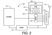
図2は、DRxフロントエンドモジュール(FEM)208を含むダイバーシティ受信器(DRx)構成200を例示する。DRx構成200は、ダイバーシティ信号を受信し、フィルタアセンブリ272を介して当該ダイバーシティ信号をDRx FEM150に与えるように構成されたダイバーシティアンテナ170を含む。フィルタアセンブリ272は、例えば、目標とする周波数範囲内の信号を、デジェネレーションスイッチング回路230に結合されたマルチ入力増幅器220への各経路に沿うように選択的に向けるべく構成されたマルチプレクサを含み得る。信号は、例えば、セルラー信号(例えば低、中、高及び/又は超高帯域のセルラー周波数)、WLAN信号、BLUETOOTH(登録商標)信号、GPS信号等を含むがこれらに限られない無線周波数(RF)信号としてよい。
FIG. 2 illustrates a diversity receiver (DRx)
DRx FEM208は、フィルタアセンブリ272から受信したダイバーシティ信号に処理を施すように構成される。例えば、DRx FEM208は、ダイバーシティ信号を、セルラー及び/又はWLAN周波数帯域を含み得る一つ以上のアクティブ周波数帯域へとフィルタリングするように構成することができる。制御器102は、目標とするフィルタに信号を選択的に向けてフィルタリングを達成するべく、DRx FEM208を制御するように構成することができる。他例として、DRx FEM208は、増幅器220を使用して、フィルタリングされた信号の一つ以上を増幅するように構成され得る。それを目的として、DRx FEM208は、フィルタ、低雑音増幅器、帯域選択スイッチ、整合回路及び他のコンポーネントを含み得る。制御器102は、DRx FEM208を通るダイバーシティ信号用の経路をインテリジェントに選択するべく、DRx FEM 208におけるコンポーネントと相互作用をするように構成することができる。
The
DRx FEM208は、処理されたダイバーシティ信号の少なくとも一部分を送受信器104に送信する。送受信器104は、制御器102によって制御することができる。いくつかの実装において、制御器102は、送受信器104内に実装することができる。
The
DRx FEM208は、複数の利得モードを与えるように構成することができる。複数の利得モードに対し、デジェネレーションスイッチング回路230の可変インピーダンス段232により、異なるインダクタンスを与えることができる。一つ以上の利得モードにおいて、可変インピーダンス段232のスイッチ234を、増幅器220に結合されたインピーダンス(例えばインダクタンス)を選択するように構成することができる。これは、例えば、増幅プロセスの線形性を改善するように行うことができる。このような選択可能インピーダンスは、マルチ入力増幅器アーキテクチャに埋め込むことができる。
The
いくつかの実施形態において、増幅段に結合された選択可能インピーダンス、例えばLNA、の利用により、線形性及び/又はIIP3を改善することができる。スイッチ234を有する可変インピーダンス段232により、有益なことに、特定の利得モード及び/又は信号振幅のために望ましい又は目標とするインピーダンスに、増幅器220を結合することが可能となり得る。いくつかの実施形態において、DRx構成200は、低利得モードで動作するときに増幅をバイパスし、他の利得モードで動作するときに増幅器220で信号を増幅するように構成される。これにより、有利なことに、DRx構成200が、特定の利得モードにおける線形性を改善することができる。
In some embodiments, the use of selectable impedances coupled to the amplification stage, such as LNA, can improve linearity and / or IIP3. The
いくつかの実施形態において、増幅器220は、複数の入力信号を受信して単数の出力信号を与えるように構成される。一定の実施形態において、増幅器220は、複数の入力信号を受信して対応する複数の出力信号を与えるように構成することができる。フィルタアセンブリ272は、特定の周波数帯域に対応する信号を、増幅器220への指定経路に沿うように向けるべく構成することができる。一定の実装において、増幅器220は、受信した信号に対し異なる利得モードを与えることができる。可変インピーダンス段232は、増幅器220に結合されたスイッチ234を使用して、異なるインピーダンスを選択することができる。選択されたインピーダンスは、少なくとも部分的に、増幅器220の利得モードに基づく。一定の実装において、増幅器220は、バイパス構成においては信号がバイパス経路を通過するように動作することができ、増幅構成においては信号が増幅経路を通過するように動作することができる。選択されたインピーダンスは、可変インピーダンス段232により与えられる。これにより、有利なことに、DRx FEM208は、線形性(例えばIIP3)及び/又は雑音指数(NF)へのマイナスの影響を、バイパス経路及び/又は可変インピーダンスを選択的に与えることがない構成と比べて低減している間に、可変利得及び/又は複数の利得モードを与えることができる。増幅器220は、望ましい又は目標とする増幅を与えるように構成された任意の適切な増幅器回路を含み得る。いくつかの実施形態において、増幅器220は低雑音増幅器(LNA)回路を含み、これは、複数の入力部又はマルチ入力LNAにおいて受信された複数の周波数帯域(例えばセルラー周波数帯域及び/又はWLAN周波数帯域)からの信号を増幅するべく構成される。しかしながら、ここに記載される実施形態が、低雑音増幅器を利用する実装に限られず、任意の様々な増幅器を使用する実装も含むことを理解すべきである。
In some embodiments, the
増幅器220は、複数の利得モードに少なくとも部分的に基づいて信号を増幅するように構成することができる。例えば、増幅器220は、第1利得モードのために第1の増幅又は利得を与え、第2利得モードのために第2の増幅又は利得を与え等のように構成することができる。増幅器220は、増幅器220に与えられる利得を制御する制御器102によって制御することができる。例えば、制御器102は、望ましい又は目標とする利得を示す信号を増幅器220に与えることができ、増幅器220は目標とする利得を与えることができる。制御器102は、例えば、無線デバイスにおける他のコンポーネントから、目標とする利得の指標を受信し、当該指標に少なくとも部分的に基づいて増幅器220を制御することができる。同様に、デジェネレーションスイッチング回路230は、増幅器220の利得モード及び/又は目標とする利得に少なくとも部分的に基づいて制御することができる。
The
制御器102は、あつらえられたインピーダンスを選択的に与えるべくDRx FEM208を制御するように構成することができる。例えば、制御器102及びDRx FEM208は、利得モードに少なくとも部分的に基づいて目標とするインピーダンスを与えるべく、可変インピーダンス段232を制御してスイッチ234を構成することができる。他例として、制御器102及びDRx FEM208は、少なくとも部分的に利得モードに基づいてバイパス経路を与えるべく、増幅器を制御することができる。他例として、制御器102及びDRx FEM208は、増幅器220を使用して複数の利得モードを与えることができる。
The
可変利得増幅器のアーキテクチャ例 Variable gain amplifier architecture example
フロントエンドモジュールは一般に、受信した信号を増幅するべく、低雑音増幅器(LNA)のような増幅器を含む。様々な利得モードを与える無線デバイスにおいて、性能を改善するべく、可変の又はあつらえられたインピーダンスを利得段に選択的に与えることが有利となり得る。同様に、少なくとも一つの利得モードに対し、性能を改善する(例えば線形性を改善する)べく利得段をバイパスすることが有利となり得る。 Front-end modules generally include an amplifier such as a low noise amplifier (LNA) to amplify the received signal. In wireless devices that provide various gain modes, it may be advantageous to selectively provide variable or tailored impedance to the gain stage in order to improve performance. Similarly, for at least one gain mode, it may be advantageous to bypass the gain stage to improve performance (eg, improve linearity).
したがって、ここに与えられるのは、可変利得増幅器の利得モードに少なくとも部分的に依存してデジェネレーションブロック及び/又はフィードバックブロックに可変の又はあつらえられたインピーダンスを選択的に与える可変利得増幅器である。これにより、有利なことに、一つ以上の利得モードにおいて性能ペナルティが低減又は排除される。さらに、可変インピーダンスを、目標とする利得モードにおける増幅プロセスの線形性を改善するように構成することができる。同様に、可変利得増幅器は、信号品質を改善するべく、低利得モードにおいて低損失バイパスモードを与えるように構成することができる。 Thus, given here is a variable gain amplifier that selectively provides variable or tailored impedance to the degeneration block and / or feedback block depending at least in part on the gain mode of the variable gain amplifier. This advantageously reduces or eliminates performance penalties in one or more gain modes. In addition, the variable impedance can be configured to improve the linearity of the amplification process in the target gain mode. Similarly, the variable gain amplifier can be configured to provide a low loss bypass mode in the low gain mode to improve signal quality.
図3Aは、マルチ入力利得段312を含む可変利得増幅器構成例310aを例示する。マルチ入力利得段312は、多数の入力を受信して当該受信した信号を利得段320によって選択的に増幅するか又はバイパスブロック340を通るバイパス経路を与えるように構成される。利得段320は、デジェネレーションスイッチングブロック330に結合される。デジェネレーションスイッチングブロック330は、可変利得増幅器構成310aの利得モードに少なくとも部分的に基づいてあつらえられたインピーダンスを選択的に与えるように構成される。一定の実装において、マルチ入力利得段312は、別個の入力ポートにおいて多数の信号を受信するように構成される。別個の入力ポートはそれぞれが、一つ以上の特定のセルラー周波数帯域にある信号を受信するように構成される。例えば、第1帯域の信号が第1入力ポートで受信され、第2帯域の信号が第2入力ポートで受信され、第3帯域の信号が第3入力ポートで受信される。
FIG. 3A illustrates a variable gain amplifier configuration example 310a including a
可変利得増幅器310aは、スイッチングネットワークを使用することなくマルチ入力処理を与えるように構成することができる。可変利得増幅器310aは、デジェネレーションスイッチングブロック330の使用を通じて相対的に高い線形性を達成するように構成することができる。一定の実装において、バイパスブロック340はシャントスイッチを含む。シャントスイッチは、かかるスイッチを有する構成と比べて高い入力対出力分離性を与えることができる。可変利得増幅器310aは、入力部からの信号を、バイパスブロック340を通るが利得段320を通らないように向けることによって低損失ダイレクトバイパスモードを与えるように構成することができる。低損失ダイレクトバイパスモードは、例えば低利得モードに実装することができる。
The
可変利得増幅器310aは、電圧を電流利得段320に与えるマルチ入力利得段312を含む。マルチ入力利得段312は、入力間の分離性を与えるように構成することができる。いくつかの実施形態において、可変利得増幅器310aは、各入力部に対するデジェネレーションスイッチングブロック330を含んで入力部をさらに分離させることができる。
The
デジェネレーションスイッチングブロック330は、インピーダンスを利得段320入力部に与えるように構成される。このようにして、処理チェーンにおける前段と整合する電力及び/又は雑音を与えることにより、性能を改善することができる。デジェネレーションスイッチングブロック330は、フィードバックメカニズムを与えることにより、利得段320の線形性を改善するように構成することができる。いくつかの実施形態において、デジェネレーションスイッチングブロック330は、第1利得モードに対して第1インピーダンスを与え、第2利得モードに対して第2インピーダンスを与えるように構成される。デジェネレーションスイッチングブロック330が与える選択されたインピーダンスはまた、利得段320の線形性も改善するように構成することができる。可変利得増幅器310aは、バイパスモードにおいてデジェネレーションスイッチングブロック330をバイパスするように構成することができる。このようにして、利得段320を通過する漏洩電流を低減又は最小化することにより、線形性能を改善することができる。
The
バイパスブロック340は、多数の入力部からの信号を受信するべく、及び利得段320又はデジェネレーションスイッチングブロック330を通過しない出力部への経路を与えるべく、構成される。バイパスブロック340は、可変利得増幅器310aが与える利得モードの一つ以上において入力部と出力部とを分離する役割を果たすコンポーネントを含み得る。
The
中間利得モードフィードバックブロック350aは、可変利得増幅器310aが与える利得モードの部分集合に対してアクティブにされるように構成される。中間利得モードフィードバックブロック350aは、目標とするインピーダンスを入力信号に与えるように構成される。これは、増幅プロセスの線形性の改善に役立ち得る。中間利得モードフィードバックブロック350aは、可変利得増幅器310a内でのフィードバックを制御するように構成することもできる。中間利得モードフィードバックブロック350aは、第2のデジェネレーションブロックを回路に含むのと同様の機能性を与えるように構成することができる。
The intermediate gain
バイパススイッチ360は、バイパスブロック340を介した入力部から出力部への経路、又は利得段320を介した入力部から出力部への経路を選択的に与えるように構成される。バイパススイッチ360は、可変利得増幅器310aの利得モードに少なくとも部分的に基づいて、望ましい経路を分離及び/又は選択する一つ以上のスイッチング素子を含み得る。
The
一定の実施形態において、可変利得増幅器310aは、複数の利得モード、例えば利得モードG0、G1、…、GNを与えるように構成することができる。G0は最高利得であり、GNはバイパスモードである。利得モードGNで動作するとき、可変利得増幅器310aは、信号を入力部からバイパスブロック340へと向けるように構成することができる。利得モードG0〜GN−1で動作するとき、可変利得増幅器310aは、利得段320を通るように信号を向けてデジェネレーションスイッチングブロック330をアクティブにするように構成することができる。デジェネレーションスイッチングブロック330は、個々の利得モードに対し又は複数群の利得モードに対し異なるインピーダンスレベルを与えるように構成することができる。これらの利得モードであっても、バイパスブロック340は、入力部と出力部との分離性を与えるべくバイパスブロック340のシャントスイッチをアクティブにすることにより、少なくとも部分的にアクティブになることができる。可変利得増幅器310aは、利得モードG0〜GN−1の一つ以上に対して中間利得モードフィードバックブロック350aをアクティブにするように構成することができる。
In certain embodiments, the
可変利得信号増幅器310aは、本開示の中間利得モードフィードバックブロック350a、バイパスブロック340、デジェネレーションスイッチングブロック330を有しない増幅器と比べ、相対的に低い雑音及び高い線形性(例えばより高いIIP3)を達成するように構成することができる。可変利得信号増幅器310aは、セルラー信号、WLAN信号、BLUETOOTH(登録商標)信号、GPS信号等のような無線周波数(RF)信号を増幅するように構成することができる。可変利得信号増幅器310aは、多数の入力部において複数の周波数帯域にわたる信号を受信して当該信号を処理することにより、広帯域性能を与えるように構成することができる。可変利得信号増幅器310aは、それぞれの入力部における信号を独立して処理するように構成することができる。可変利得信号増幅器310aは、制御器(例えば図1及び図2を参照してここに記載される制御器102)のような制御回路アセンブリが制御するように構成することができる。制御回路アセンブリは、経路を増幅経路とバイパス経路との間でインテリジェントかつ選択的に切り替えることができ、デジェネレーションスイッチングブロック330により選択的にインピーダンスを与えることができる。
The variable
3個の入力部が例示されるにもかかわらず、可変利得増幅器310aが任意数の適切な入力部を含み得ることを理解すべきである。例えば、限定なく、可変利得増幅器310aは、少なくとも2個の入力部、少なくとも4個の入力部、少なくとも8個の入力部、少なくとも16個の入力部、少なくとも32個の入力部、少なくとも64個の入力部、又は記載された範囲で少なくとも任意数の入力部を含んでよい。他例としてかつ限定なく、可変利得増幅器310aは、64個以下の入力部、32個以下の入力部、16個以下の入力、8個以下、4個以下の入力部、又は記載された範囲で任意数以下の入力部を含んでよい。
It should be understood that the
図3Bは、一定の素子の付加とともに図3Aの可変利得増幅器310aと同じコンポーネントを含む他の可変利得増幅器例310bを例示する。例えば、可変利得増幅器310bは整合ネットワーク313、318及び345を含む。入力整合ネットワーク313は、入力部において受信した信号に対してインピーダンス整合を与えるように構成される。出力整合ネットワーク318も同様に、出力負荷316と利得段320及びカスコードバッファ314を含む増幅器とに対してインピーダンス整合を与えるように構成される。バイパス整合ネットワーク345も同様に、バイパスブロック340に対してインピーダンス整合を与える。整合ネットワーク313、318、345に対し、目標とするインピーダンスを与えるべく、インダクタ及びキャパシタの任意の適切な組み合わせを使用することができる。
FIG. 3B illustrates another variable gain amplifier example 310b that includes the same components as the
可変利得増幅器310bはまた、出力負荷316と、増幅チェーンの一部としてのカスコードバッファ314とを含む。カスコードバッファ314は、電流バッファとして作用するように構成することができる。カスコードバッファ314は、利得段320と出力部との分離性を与えるように構成される。カスコードバッファ314はまた、可変利得増幅器310bの利得を改善するように構成することもできる。出力負荷316は、出力電圧振幅を生成するべく負荷を電流に与えるように構成される。出力負荷316は、入力部において受信した各帯域に対してチューニングされ又はチューニング可能となるように構成することができる。出力負荷316は、出力負荷316の抵抗をあつらえることにより、反射損失を改善し及び/又は帯域幅を増加させるように構成することができる。電圧VDDは、可変利得増幅器310bの利得モードを設定するように構成することができる。例えば、電圧VDDは、出力負荷316を介して流れる電流が低くなることが、可変利得増幅器310bの利得が低くなることに対応するように構成することができる。
The
図3Cは、図3Aの可変利得増幅器310aと同様であるが、バイパススイッチ360が除外された他の可変利得増幅器例310cを例示する。バイパススイッチ360が存在しないので、バイパスブロック340の出力は、利得段320の出力部の出力に結合される。さらに、中間利得モードフィードバックブロックが、シャットダウンスイッチブロック350cに置換されているが、シャットダウンスイッチブロック350cは、図3Aの可変利得増幅器310aにおけるように出力部に結合されているわけではない。その代わり、シャットダウンスイッチブロック350cは、増幅器310cにおける漏洩を低減するべく入力ノードを選択的に分離するように構成される。いくつかの実施形態において、これは、入力部が使用されていないときに入力ノードと基準電位ノードとの間にあるスイッチをアクティブにすることによってアクティブにすることができる。様々な実装において、スイッチは、容量素子を介して入力ノードを基準電位ノードに結合することができる。
FIG. 3C illustrates another variable gain amplifier example 310c, which is similar to the
図3Dは、一定の素子の付加とともに、図3Cの可変利得増幅器310cと同じコンポーネントを含む他の可変利得増幅器例310dを例示する。例えば、可変利得増幅器310dは、整合ネットワーク313、318及び345を含む。入力整合ネットワーク313は、入力部において受信した信号に対してインピーダンス整合を与えるように構成される。出力整合ネットワーク318も同様に、出力負荷316と利得段320及びカスコードバッファ314を含む増幅器とに対してインピーダンス整合を与えるように構成される。バイパス整合ネットワーク345も同様に、バイパスブロック340に対してインピーダンス整合を与える。整合ネットワーク313、318、345に対し、目標とするインピーダンスを与えるべく、インダクタ及びキャパシタの任意の適切な組み合わせを使用することができる。
FIG. 3D illustrates another variable gain amplifier example 310d containing the same components as the
可変利得増幅器310dはまた、出力負荷316と、増幅チェーンの一部としてのカスコードバッファ314とを含む。カスコードバッファ314は、電流バッファとして作用するように構成することができる。カスコードバッファ314は、利得段320と出力部との分離性を与えるように構成される。カスコードバッファ314はまた、可変利得増幅器310dの利得を改善するように構成することもできる。出力負荷316は、出力電圧振幅を生成するべく負荷を電流に与えるように構成される。出力負荷316は、入力部において受信した各帯域に対してチューニングされ又はチューニング可能となるように構成することができる。出力負荷316は、出力負荷316の抵抗をあつらえることにより、反射損失を改善し及び/又は帯域幅を増加させるように構成することができる。電圧VDDは、可変利得増幅器310dの利得モードを設定するように構成することができる。例えば、電圧VDDは、出力負荷316を介して流れる電流が低くなることが、可変利得増幅器310dの利得が低くなることに対応するように構成することができる。
The
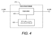
図4は、入力信号を受信して増幅された出力信号を生成するように構成された可変利得段420を含む可変利得信号増幅器410を例示する。可変利得信号増幅器410はまた、可変利得段420に結合されたデジェネレーションスイッチングブロック430も含む。デジェネレーションスイッチングブロック430は、可変利得段420の複数の異なる利得レベルを与えるべく構成することができる。
FIG. 4 illustrates a variable
図5は、様々な利得レベルを有する信号増幅器520に結合された可変インピーダンス段532を含むデジェネレーションスイッチング回路530を例示する。可変インピーダンス段532は、様々な利得レベルに関連付けられた様々なインピーダンス値を与えるように構成することができる。デジェネレーションスイッチング回路530は、可変インピーダンス段532と動作可能に関連付けられたスイッチ534を含む。スイッチ534は、可変インピーダンス段532を基準電位ノードから選択的に分離するように実装される。
FIG. 5 illustrates a
図6は、図3Bを参照してここに記載される可変利得増幅器310bと同様に構成された可変利得増幅器構成例610を例示する。可変利得増幅器610は、増幅器の実装例を実証する電気コンポーネント例を含む。しかしながら、これは実装例の単なる例示であり、本開示の範囲が、同様のアーキテクチャを包含する付加的な実装まで拡張されることを理解するべきである。
FIG. 6 illustrates a variable gain amplifier configuration example 610 configured similarly to the
可変利得増幅器構成610は、入力A、B及びCを受信して当該受信した信号を、トランジスタQ10を有するカスコードバッファ614と連動する対応トランジスタQ3、Q4及びQ5によって選択的に増幅するように構成されたマルチ入力利得段612を含む。マルチ入力利得段612はまた、入力A、B及びCそれぞれに対してスイッチングトランジスタQ6、Q7及びQ8を含むバイパスブロック340を通るバイパス経路を与えるように構成される。
The variable
マルチ入力利得段612は、デジェネレーションスイッチングブロック630に結合される。デジェネレーションスイッチングブロック630は、可変利得増幅器構成610の利得モードに少なくとも部分的に基づいてあつらえられたインピーダンスを選択的に与えるように構成される。一定の実装において、マルチ入力利得段612は、別個の入力ポートにおいて多数の信号を受信するように構成される。別個の入力ポートはそれぞれが、一つ以上の特定のセルラー周波数帯域にある信号を受信するように構成される。例えば、入力部Aが第1帯域の信号を受信し、入力部Bが第2帯域の信号を受信し、入力部Cが第3帯域の信号を受信する。いくつかの実施形態において、トランジスタQ3、Q4及びQ5はそれぞれが、入力ポート間の分離性を増加させるべく、専用のデジェネレーションスイッチングブロック630に結合され得る。これらの入力部はそれぞれ、入力インピーダンス整合を与えるべくインダクタL4、L5及びL6に結合される。
The
可変利得増幅器構成610は、スイッチングネットワークを使用することなくマルチ入力処理を与えるように構成することができる。可変利得増幅器構成610は、デジェネレーションスイッチングブロック630の使用を介して相対的に高に線形性を達成するように構成することができる。一定の実装において、バイパスブロック640は、かかるスイッチを有する構成と比べ高い入力対出力分離性を与えることができるシャントスイッチQ9を含む。可変利得増幅器構成610は、入力部からバイパスブロック640を通るように信号を向けることにより、低損失ダイレクトバイパスモードを与えるように構成することができる。低損失ダイレクトバイパスモードは、例えば低利得モードに実装することができる。
The variable
可変利得増幅器構成610は、トランジスタQ3〜Q5を含む電流利得段に電圧を与えるマルチ入力利得段312を含む。マルチ入力利得段312は、電圧を電流利得段に与えるように構成される。さらに、マルチ入力利得段312は、それぞれの入力信号を、トランジスタQ10を含むカスコードバッファ614と連動して増幅するように構成され、カスコードバッファ614は、入力インピーダンスを低下させかつ出力インピーダンスを増加させる電流バッファとして作用するように構成される。
The variable
デジェネレーションスイッチングブロック630は、マルチ入力利得段612の利得段にインピーダンスを与えるように構成される。このようにして、処理チェーンにおける前段と整合する電力及び/又は雑音を与えることにより、性能を改善することができる。デジェネレーションスイッチングブロック630は、フィードバックメカニズムを与えることにより、利得段(例えばトランジスタQ3〜Q5)の線形性を改善するように構成することができる。デジェネレーションスイッチングブロック630は、トランジスタQ2及びトランジスタQ1をそれぞれアクティブにすることにより、第1インピーダンスL1を第1利得モードに与え、L1及びL2により得られる第2インピーダンスを第2利得モードに与えるように構成することができる。デジェネレーションスイッチングブロック630が与える選択されたインピーダンスはまた、利得段の線形性を改善するように構成することもできる。可変利得増幅器構成610は、バイパスモードにおいてデジェネレーションスイッチングブロック630をバイパスするように構成することができる。このようにして、利得段を通過する漏洩電流を低減又は最小化することにより、線形性能を改善することができる。一定の実装において、デジェネレーションスイッチングブロック630は、低いインダクタンスを高い利得モードに与えるように構成することができる。デジェネレーションスイッチングブロック630が与えるインダクタンスの量は、可変利得増幅器構成610の利得モードの変化によって変更することができる。
The
バイパスブロック640は、多数の入力部からの信号を受信するべく、及び利得段(例えばトランジスタQ3〜Q5)又はデジェネレーションスイッチングブロック630を通過しない出力部への経路を与えるべく、構成される。バイパスブロック640は、トランジスタQ11及びキャパシタC1を介した出力部への単数の経路を与えるように構成される。キャパシタC1は、直流(DC)電圧を出力供給からブロックするように構成することができる。バイパスブロック640はまた、入力部を出力部から分離する補助となるようにバイパスブロック640を選択的に基準電位ノードに結合するトランジスタQ9を介したシャントスイッチを含む。バイパス整合ネットワーク645は、付加的なインピーダンス整合柔軟性を与えることができる。
The
中間利得モードフィードバックブロック650は、可変利得増幅器構成610が与える利得モードの部分集合に対してアクティブにされるように構成される。中間利得モードフィードバックブロック650は、目標とするインピーダンスを入力信号に与えるように構成される。これは、増幅プロセスの線形性の改善に役立ち得る。システムにおけるフィードバックの量を制御するべく、RC整合ネットワーク651を使用することができる。さらに、RC整合ネットワーク651は、DC電圧のためのブロックとして機能するように構成することができる。RC整合ネットワーク651は、振幅及び位相のフィードバック挙動を制御するように構成することができる。RC整合ネットワーク651は、キャパシタ、抵抗器、直列のキャパシタ及び抵抗器、又はキャパシタ、抵抗器及び他のコンポーネントの任意の適切な組み合わせを含み得る。中間利得モードフィードバックブロック650はまた、可変利得増幅器610内のフィードバックを制御するように構成することもできる。中間利得モードフィードバックブロック650は、第2のデジェネレーションブロックを回路に含むのと同様の機能性を与えるように構成することができる。
The intermediate gain
アクティブになると、入力部A、B及びCそれぞれからの信号が、ポイントA、B及びCにおいて中間利得フィードバックブロック650に入り、ポイントDにおいて当該ブロックから出る。このポイントDは、出力整合ネットワーク618及びバイパススイッチ660に先立って回路に結合される。言い換えると、中間利得モードフィードバックブロック650は、入力部A、B及びCそれぞれを、トランジスタQ14〜Q16及びQ18を介して出力部に結合することができる。付加的なトランジスタQ17は、バイパスブロック640と同様にシャントスイッチを基準電位ノードに与えるように構成することができる。ポイントDは、出力整合ネットワーク618の先となるように、出力整合ネットワーク618内となるように、又は出力整合ネットワーク618の後となるように位置決めすることができる。中間利得モードフィードバックブロック650は、入力と出力との相殺を生成するべく構成することができるので、ポイントDは、性能を改善するべく可変利得増幅器構成610内に位置決めすることができる。
When activated, signals from inputs A, B and C each enter the intermediate
バイパススイッチ660は、入力部A、B及びCからバイパスブロック640を介して出力部への経路、又は入力部A、B及びCから利得段素子及び増幅器素子(例えばカスコードバッファ614及び出力整合ネットワーク618)を介して出力部への経路を選択的に与えるように構成される。バイパススイッチ660は、増幅経路と出力部との接続を制御するトランジスタQ12と、バイパス経路と出力部との接続を制御するトランジスタQ13とを含む。バイパススイッチ660は、可変利得増幅器610の利得モードに少なくとも部分的に基づいて制御することができる。
The
整合ネットワーク618及び645は、目標とするインピーダンスを与えるべく使用することができるインダクタ及びキャパシタの任意の適切な組み合わせを含み得る。出力整合ネットワーク618は、出力負荷616と利得段(例えばトランジスタQ3〜Q5)及びカスコードバッファ614を含む増幅器とに対してインピーダンス整合を与えるように構成される。バイパス整合ネットワーク645も同様に、バイパスブロック640のためのインピーダンス整合を与える。
Matching
可変利得増幅器610は、出力負荷616と、増幅経路の一部としてのカスコードバッファ614とを含む。カスコードバッファ614は、電流バッファとして作用するべく構成されたトランジスタQ10を含む。カスコードバッファ614は、利得段と出力部との分離性を与えるように構成される。カスコードバッファ614はまた、可変利得増幅器610の利得を改善するように構成することもできる。出力負荷616は、出力電圧振幅を生成するべく付加を電流に与えるように構成される。出力負荷616は、入力部において受信した各帯域に対してチューニングされ又はチューニング可能となるように構成することができる。例えば、出力負荷は、特定のセルラー周波数帯域に対してチューニング可能な可変キャパシタC2を含む。出力負荷616はまた、出力負荷616の抵抗R1をあつらえることにより、反射損失を改善し及び/又は帯域幅を増加させるように構成することもできる。
The
電圧VDDは、可変利得増幅器310bの利得モードを設定するように構成することができる。例えば、電圧VDDは、出力負荷316を介して流れる電流が低くなることが、可変利得増幅器310bの利得が低くなることに対応するように構成することができる。
The voltage VDD can be configured to set the gain mode of the
図7A〜図7Cは、図6の可変利得信号増幅器構成610の動作モードの複数例を例示する。図7Aは、一つ以上の高利得モードにおける動作を例示する。これらの高利得モードにおいて、バイパスブロック640は、シャントスイッチQ9を除いてアクティブ解除される。入力部A、B及びCにおいて受信した信号は、トランジスタQ3〜Q5を含む利得段を通るようにかつカスコードバッファ614を通るように向けられ、出力整合ネットワーク618及びバイパススイッチ660を通って出力部に至る。バイパススイッチは、これらの高利得モードにおいてQ12をアクティブにし、Q13をアクティブ解除する。さらに、これらの高利得モードにおいて、トランジスタQ2がオンにされ、トランジスタQ1はオフにされるので、デジェネレーションスイッチングブロック630を介して利得段に与えられるインダクタンスはL1となる。これらの高利得モードにおいて、中間利得モードフィードバックブロック650もアクティブ解除される。
7A-7C exemplify a plurality of operating modes of the variable gain
図7Bは、一つ以上の中間利得モードにおける動作を例示する。これらのモードはまた、低利得高線形性モードと称することができる。これらの中間利得モードでの動作は、顕著な差異を有する一つ以上の高利得モードの動作と同様である。第一に、デジェネレーションブロック630において、トランジスタQ2がオフにされ、トランジスタQ1がオンにされるので、デジェネレーションスイッチングブロック630を介して利得段に与えられるインダクタンスは、L1及びL2の双方により与えられる。よって、利得モードが低くなると増加したインピーダンスが得られ、又は利得モードが高くなると減少したインピーダンスが得られる。第二に、中間利得モードフィードバックブロック650がアクティブにされる。これにより、第2のデジェネレーションブロックを加えたのと同様に、回路への付加的なフィードバックが得られる。
FIG. 7B illustrates operation in one or more intermediate gain modes. These modes can also be referred to as low gain high linearity modes. The operation in these intermediate gain modes is similar to the operation in one or more high gain modes with significant differences. First, in the
図7Cは、一つ以上の低利得モードにおける動作を例示する。これらの低利得モードでは、バイパスブロック640がアクティブにされ、利得段トランジスタQ3〜Q5がアクティブ解除される。入力部A、B及びCにおいて受信した信号は、バイパスブロック640を介し、バイパス整合ネットワーク645及びバイパススイッチ660を介し、出力部に向けられる。これらの低利得モードにおいて、バイパススイッチはQ13をアクティブにし、Q12をアクティブ解除する。さらに、デジェネレーションスイッチングブロック630をアクティブ解除するべくトランジスタQ1及びQ2はオフにされ、利得段トランジスタQ3〜Q5を通る漏洩電流を低減又は最小化することにより、線形性能が改善される。中間利得モードフィードバックブロック650もまた、これらの低利得モードにおいてアクティブ解除される。
FIG. 7C illustrates operation in one or more low gain modes. In these low gain modes, the
図8は、図6の可変利得信号増幅器構成610と同様であるが、バイパススイッチ660が除外された可変利得信号増幅器810を例示する。バイパススイッチを除外することにより、バイパス整合ネットワーク645の出力がその代わりに、出力整合ネットワーク618の入力ノードに結合される。この構成では、増幅経路又はバイパス経路の選択を制御するバイパススイッチが存在しない。むしろ、利得段の選択されたトランジスタ(例えばトランジスタQ3〜Q5)、及びバイパスブロックの選択されたトランジスタ(例えばトランジスタQ6〜Q8)が、バイパス経路又は増幅経路を与えるべく選択的にアクティブにされ及びアクティブ解除される。
FIG. 8 illustrates a variable
図9は、図6の可変利得信号増幅器構成610と同様であるが、中間利得モードフィードバックモジュールの代わりにシャットダウンスイッチブロック950を有する可変利得信号増幅器910を例示する。この構成では、出力整合ネットワーク618の出力ノードにおいてシャットダウンスイッチブロック950が増幅経路に結合されないので、ポイントDが除外される。その代わり、シャットダウンスイッチブロック950は、入力ノードA、B及びCを選択的に分離するべく構成されたトランジスタQ14〜Q16及びキャパシタC3〜C5を含む。いくつかの実施形態において、シャットダウンスイッチブロック950はキャパシタC3〜C5を含まない。シャットダウンスイッチブロック950は、対応する入力部が使用されていないときにスイッチをオンにする(例えばトランジスタをアクティブにする)ように構成することができる。これは、増幅器構成における漏洩を低減又は排除するべく、当該入力部をグランドに対してシャットオフするように行うことができる。
FIG. 9 illustrates a variable
図10は、図9の可変利得信号増幅器構成910と同様であるが、バイパススイッチ660が除外された可変利得信号増幅器1010を例示する。図8の可変利得信号増幅器810と同様に、バイパススイッチが除外されることにより、バイパス整合ネットワーク645の出力が出力整合ネットワーク618の入力ノードに結合される結果となる。この構成では、増幅経路又はバイパス経路の選択を制御するバイパススイッチが存在しない。むしろ、利得段の選択されたトランジスタ(例えばトランジスタQ3〜Q5)、及びバイパスブロックの選択されたトランジスタ(例えばトランジスタQ6〜Q8)が、バイパス経路又は増幅経路を与えるべく選択的にアクティブにされ及びアクティブ解除される。
FIG. 10 illustrates a variable
製品及びアーキテクチャの例 Product and architecture examples
図11は、いくつかの実施形態において、特徴(例えば図1〜図10)の組み合わせを有するダイバーシティ受信器構成のいくつか又はすべてを含むダイバーシティ受信器構成のいくつか又はすべてを、全体的又は部分的にモジュールに実装することができる。かかるモジュールは、例えば、フロントエンドモジュール(FEM)としてよい。かかるモジュールは、例えば、ダイバーシティ受信器(DRx)FEMとしてよい。かかるモジュールは、例えば、マルチ入力・マルチ出力(MiMo)モジュールとしてよい。 FIG. 11 shows, in some embodiments, some or all of the diversity receiver configurations including some or all of the diversity receiver configurations having a combination of features (eg, FIGS. 1-10), in whole or in part. Can be implemented in a module. Such a module may be, for example, a front-end module (FEM). Such a module may be, for example, a diversity receiver (DRx) FEM. Such a module may be, for example, a multi-input / multi-output (MiMo) module.
図11の例において、モジュール1108はパッケージ基板1101を含み、かかるパッケージ基板1101に一定数のコンポーネントが取り付けられる。例えば、(フロントエンド電力管理集積回路[FE−PIMC]を含み得る)制御器1102、組み合わせアセンブリ1106、ここに記載される一つ以上の特徴を有する利得段1120及びデジェネレーションスイッチングブロック1130を含む可変利得増幅器アセンブリ1110、並びに(一つ以上の帯域通過フィルタを含み得る)フィルタバンク1108を、パッケージ基板1101上に及び/又はパッケージ基板1101内に取り付け及び/又は実装することができる。一定数のSMTデバイス1105のような他のコンポーネントを、パッケージ基板1101に取り付けることもできる。様々なコンポーネントのすべてがパッケージ基板1101上にレイアウトされるように描かれているにもかかわらず、一定のコンポーネントを他のコンポーネントの上に実装することもできることが理解される。
In the example of FIG. 11, the
図12は、いくつかの実施形態において、特徴(例えば図1〜図10)の組み合わせを有するダイバーシティ受信器構成のいくつか又はすべてを含むダイバーシティ受信器構成のいくつか又はすべてを、全体的又は部分的にアーキテクチャに実装することができる。かかるアーキテクチャは一つ以上のモジュールを含み、ダイバーシティ受信器(DRx)フロントエンド機能のようなフロントエンド機能を与えるように構成することができる。 FIG. 12 shows, in some embodiments, some or all of the diversity receiver configurations including some or all of the diversity receiver configurations having a combination of features (eg, FIGS. 1-10), in whole or in part. Can be implemented in the architecture. Such an architecture may include one or more modules and be configured to provide front-end functionality such as diversity receiver (DRx) front-end functionality.
図12の例において、アーキテクチャ1208は、(フロントエンド電力管理集積回路[FE−PIMC]を含み得る)制御器1202、組み合わせアセンブリ1206、ここに記載される一つ以上の特徴を有する利得段1220及びデジェネレーションスイッチングブロック1230を含む可変利得増幅器アセンブリ1210、並びに(一つ以上の帯域通過フィルタを含み得る)フィルタバンク1208を、パッケージ基板1201上に及び/又はパッケージ基板1201内に取り付け及び/又は実装することができる。一定数のSMTデバイス1205のような他のコンポーネントもまた、アーキテクチャ1208に実装することができる。
In the example of FIG. 12,
いくつかの実装において、ここに記載される一つ以上の特徴を有するデバイス及び/又は回路は、無線デバイスのようなRF電子デバイスに含めることができる。かかるデバイス及び/又は回路は、無線デバイスに直接、ここに記載されるモジュラー形態で、又はこれらの一定の組み合わせで実装することができる。いくつかの実施形態において、かかる無線デバイスは、例えば、携帯電話機、スマートフォン、電話機能あり又はなしのハンドヘルド無線デバイス、無線タブレット等を含み得る。 In some implementations, devices and / or circuits having one or more features described herein can be included in RF electronic devices such as wireless devices. Such devices and / or circuits can be implemented directly on the wireless device in the modular form described herein, or in certain combinations thereof. In some embodiments, such wireless devices may include, for example, mobile phones, smartphones, handheld wireless devices with or without telephone functionality, wireless tablets, and the like.
図13は、ここに記載される一つ以上の有利な特徴を有する無線デバイス例1300を描く。ここに記載される一つ以上の特徴を有する一つ以上のモジュールの文脈において、かかるモジュールは一般に、(例えばフロントエンドモジュールとして実装可能な)破線の囲い1306、及び(例えばフロントエンドモジュールとして実装可能な)ダイバーシティ受信器(DRx)モジュール1308によって描かれる。
FIG. 13 depicts an
図13を参照すると、複数の電力増幅器(PA)1382がそれぞれ、送受信器1304からRF信号を受信することができる。送受信器1304は、増幅及び送信対象のRF信号を生成するように、及び受信信号を処理するように、構成されて動作することができる。送受信器1304は、ユーザに適したデータ及び/又は音声信号と送受信器1304に適したRF信号との間の変換を与えるように構成されたベース帯域サブシステム1305と相互作用をするように示される。送受信器1304はまた、無線デバイス1300の動作を目的として電力を管理するべく構成された電力管理コンポーネント1307と通信することもできる。かかる電力管理はまた、ベース帯域サブシステム1305並びにモジュール1306及び1308の動作も制御することができる。
Referring to FIG. 13, each of the plurality of power amplifiers (PAs) 1382 can receive RF signals from the transmitter /
ベース帯域サブシステム1305は、ユーザに与えられ及びユーザから受信する音声及び/又はデータの様々な入力及び出力を容易にするべくユーザインタフェイス1301に接続されるように示される。ベース帯域サブシステム1305はまた、無線デバイスの動作を容易にするべく及び/又はユーザのための情報格納を与えるべく構成されたメモリ1303にも接続される。メモリ1303は、データ及び/又は命令を格納するように構成される。
The
無線デバイス例1300において、PA1382の出力は、(各整合回路1384を介して)整合されて各デュプレクサ1386へと引き回される。かかる増幅されかつフィルタリングされた信号は、送信を目的としてスイッチングネットワーク1309を介して一次アンテナ1360へと引き回すことができる。いくつかの実施形態において、デュプレクサ1386により、共通アンテナ(例えば一次アンテナ1360)を使用して送信動作及び受信動作を同時に行うことが許容され得る。図13において、受信信号は、ここに開示の可変利得増幅器の特徴及び利益を与える可変利得増幅器アセンブリ1310aへと引き回されるように示される。DRxモジュール1308も、同様の可変利得増幅器アセンブリ1310bを含む。
In wireless device example 1300, the output of PA1382 is matched (via each matching circuit 1384) and routed to each
無線デバイス例1300において、一次アンテナ1360において受信した信号は、フロントエンドモジュール1306の可変利得増幅器1310aに送信され得る。可変利得増幅器1310aは、利得段1320及びデジェネレーションスイッチングブロック1330を含み得る。可変利得増幅器1310aは、入力部1311において複数の信号を受信し、出力部1319において複数の処理済み信号を出力するように構成される。可変利得増幅器1310aは、利得モードに少なくとも部分的に基づいて信号を増幅するべく、及び利得モードに少なくとも部分的に基づいてデジェネレーションスイッチングブロック330を介して目標とするインピーダンスを与えるべく、構成される。これは、本記載の特徴の一つ以上を含むわけではない可変利得増幅器と比べ、信号の線形性を改善するように行うことができる。少なくとも一つの低利得モードでは、利得段1320及びデジェネレーションスイッチングブロック1330はバイパスしてよい。少なくとも一つの非低利得モードでは、ここに記載される中間利得モードフィードバックモジュールを介してのように、増幅プロセスの線形性を改善するべく可変利得増幅器1310aにおいて付加的なフィードバックを与えることができる。
In the wireless device example 1300, the signal received by the
無線デバイスはまた、ダイバーシティアンテナ1370、及びダイバーシティアンテナ1370から信号を受信するダイバーシティ受信器モジュール1308も含む。ダイバーシティ受信モジュール1308は、フロントエンドモジュール1306における可変利得増幅器1310aと同様の可変利得増幅器1310bを含む。ダイバーシティ受信器モジュール1308及び可変利得増幅器1310bは、受信した信号を処理し、処理した信号を送受信器1304に送信する。いくつかの実施形態において、ダイプレクサ、トライプレクサ、又は他のマルチプレクサ若しくはフィルタアセンブリを、ここに記載されるように、ダイバーシティアンテナ1370とダイバーシティ受信器モジュール1370との間に含めることができる。
The wireless device also includes a
本開示の一つ以上の特徴を、ここに記載される様々なセルラー周波数帯域とともに実装することができる。かかる帯域の例を表1に挙げる。理解されることだが、当該帯域の少なくともいくつかは、サブ帯域に分割することができる。本開示の一つ以上の特徴が、表1の例のような指定を有しない周波数範囲とともに実装し得ることも理解される。無線周波数(RF)及び無線周波数信号との用語が、少なくとも表1に挙げられる周波数を含む信号を言及することが理解される。

本明細書及び特許請求の範囲全体にわたり、文脈上そうでないことが明らかでない限り、「含む」、「備える」等の単語は、排他的又は網羅的な意味とは反対の包括的意味に、すなわち「〜を含むがこれらに限られない」との意味に解釈すべきである。ここで一般に使用される単語「結合」は、直接接続されるか又は一つ以上の中間要素を介して接続されるかのいずれかとなり得る2以上の要素を言及する。加えて、単語「ここ」、「上」、「下」及び同様の趣旨の単語は、本アプリケーションにおいて使用される場合、本アプリケーション全体を言及し、本アプリケーションの任意の特定部分を言及するわけではない。文脈が許容する場合、単数又は複数を使用する所定実施形態の上記説明における単語はそれぞれ、複数又は単数をも含み得る。2以上の項目のリストを言及する単語「又は」及び「若しくは」は、当該単語の以下の解釈のすべてをカバーする。すなわち、当該リストの任意の項目、当該リストのすべての項目、及び当該リストの項目の任意の組み合わせである。 Throughout the specification and claims, words such as "include" and "provide" have an inclusive meaning as opposed to an exclusive or exhaustive meaning, unless it is clear in the context that this is not the case. It should be interpreted as meaning "including but not limited to". The commonly used word "join" here refers to two or more elements that can be either directly connected or connected via one or more intermediate elements. In addition, the words "here", "above", "below" and similar words, when used in this application, refer to the entire application and do not refer to any particular part of the application. No. Where the context allows, the words in the above description of a given embodiment using the singular or plural may also include the plural or singular, respectively. The words "or" and "or" referring to a list of two or more items cover all of the following interpretations of the word. That is, any item in the list, all items in the list, and any combination of items in the list.
本発明の実施形態の上記詳細な説明は、排他的であることすなわち本発明を上記開示の正確な形態に制限することを意図しない。本発明の及びその例の特定の実施形態が例示を目的として上述されたが、当業者が認識するように、本発明の範囲において様々な均等の修正も可能である。例えば、プロセス又はブロックが所与の順序で提示されるが、代替実施形態は、異なる順序でステップを有するルーチンを行うこと又はブロックを有するシステムを用いることができ、いくつかのプロセス又はブロックは削除、移動、追加、細分化、結合、及び/又は修正することができる。これらのプロセス又はブロックはそれぞれが、様々な異なる態様で実装することができる。また、プロセス又はブロックが直列的に行われるように示されることがあるが、これらのプロセス又はブロックは、その代わりに、並列して行い又は異なる時に行うこともできる。 The above detailed description of embodiments of the invention is not intended to be exclusive, i.e., to limit the invention to the exact embodiments of the disclosure. Although specific embodiments of the present invention and examples thereof have been described above for purposes of illustration, various equal modifications are possible within the scope of the invention, as will be appreciated by those skilled in the art. For example, processes or blocks are presented in a given order, but alternative embodiments may be to perform routines with steps in different orders or to use a system with blocks, some processes or blocks being deleted. Can be moved, added, subdivided, combined, and / or modified. Each of these processes or blocks can be implemented in a variety of different ways. It may also be indicated that the processes or blocks are performed in series, but these processes or blocks may instead be performed in parallel or at different times.
ここに与えられた本発明の教示は、必ずしも上述のシステムに限られることがなく、他のシステムにも適用することができる。上述の様々な実施形態要素及び行為は、さらなる実施形態を与えるべく組み合わせることができる。 The teaching of the present invention given herein is not necessarily limited to the above-mentioned system, and can be applied to other systems. The various embodiment elements and actions described above can be combined to give further embodiments.
本発明のいくつかの実施形態が記載されたが、これらの実施形態は、例のみとして提示されており、本開示の範囲を制限することを意図しない。実際のところ、ここに記載される新規な方法及びシステムは、様々な他の形態で具体化することができる。さらに、ここに記載される方法及びシステムの形態における様々な省略、置換及び変更が、本開示の要旨から逸脱することなくなし得る。添付の特許請求の範囲及びその均等物が、本開示の範囲及び要旨に収まるかかる形態又は修正をカバーすることが意図される。
Although some embodiments of the invention have been described, these embodiments are presented by way of example only and are not intended to limit the scope of the present disclosure. In fact, the novel methods and systems described herein can be embodied in various other forms. Moreover, various omissions, substitutions and changes in the methods and forms of the system described herein may be made without departing from the gist of the present disclosure. It is intended that the appended claims and their equivalents cover such forms or modifications that fall within the scope and gist of the present disclosure.
Claims (18)
複数の入力部において複数の入力信号を受信して増幅された出力信号を生成するべく構成された可変利得段であって、個々の受信した信号が、異なる信号周波数帯域内の周波数を有する、可変利得段と、
前記可変利得段に結合されて前記可変利得段の複数の利得レベルを与えるべく構成されたデジェネレーションスイッチングブロックと、
前記可変利得段の前記複数の入力部に結合された中間利得モードフィードバックブロックと
を含み、
前記中間利得モードフィードバックブロックは、前記複数の利得レベルの部分集合のためにフィードバックを前記可変利得段に与えるように構成され、
前記可変利得信号増幅器は、少なくとも部分的に利得モードに基づいて、
前記可変利得段をバイパスして前記複数の入力部から前記可変利得信号増幅器の一つの出力部へと向かうバイパス経路と、
前記可変利得段を通過する増幅経路と
を選択的に与えるように構成される可変利得信号増幅器。 It is a variable gain signal amplifier.
A variable gain stage configured to receive a plurality of input signals and generate an amplified output signal in a plurality of input units, wherein each received signal has a frequency within a different signal frequency band. Gain stage and
A degeneration switching block coupled to the variable gain stage and configured to provide multiple gain levels of the variable gain stage.
And a intermediate gain mode feedback block coupled to said plurality of inputs of the variable gain stage,
The intermediate gain mode feedback block is configured to provide feedback to the variable gain stage for a subset of the plurality of gain levels.
The variable gain signal amplifier is at least partially based on the gain mode.
A bypass path that bypasses the variable gain stage and goes from the plurality of input units to one output unit of the variable gain signal amplifier.
A variable gain signal amplifier configured to selectively provide an amplification path through the variable gain stage.
前記第1の利得レベルは前記第2の利得レベルよりも低い請求項4の可変利得信号増幅器。 The first custom-made impedance is larger than the second custom-made impedance.
The variable gain signal amplifier according to claim 4, wherein the first gain level is lower than the second gain level.
前記バイパスブロックは、前記可変利得段を含まないバイパス経路を与えるべく、前記複数の利得レベルの低利得レベルにおいてアクティブにされるように構成される請求項1の可変利得信号増幅器。 Further comprising a bypass block coupled to said plurality of inputs of the variable gain stage,
The variable gain signal amplifier according to claim 1, wherein the bypass block is configured to be activated at low gain levels of the plurality of gain levels to provide a bypass path that does not include the variable gain stage.
可変利得段、デジェネレーションスイッチングブロック、及び中間利得モードフィードバックブロックを含む可変利得信号増幅器と、
フィルタアセンブリと、
制御器と
を含み、
前記可変利得段は、複数の入力部において複数の入力信号を受信して増幅された出力信号を生成するべく構成され、個々の受信した信号が、異なる信号周波数帯域内の周波数を有し、
前記デジェネレーションスイッチングブロックは前記可変利得段に結合されて前記可変利得段の複数の利得レベルを与えるべく構成され、
前記中間利得モードフィードバックブロックは前記可変利得段の前記複数の入力部に結合され、
前記中間利得モードフィードバックブロックは、前記複数の利得レベルの部分集合のためにフィードバックを前記可変利得段に与えるように構成され、
前記フィルタアセンブリは、前記可変利得信号増幅器の選択入力部に周波数帯域を向けるように前記可変利得信号増幅器に結合され、
前記制御器は、複数の利得モードを与えるべく前記可変利得信号増幅器を制御するように実装され、
低利得モードにおいて、前記可変利得信号増幅器は信号を、前記可変利得段をバイパスする経路に沿って前記複数の入力部から前記可変利得信号増幅器の一つの出力部へと向けるフロントエンドアーキテクチャ。 It ’s a front-end architecture,
A variable gain signal amplifier that includes a variable gain stage, a degeneration switching block, and an intermediate gain mode feedback block,
With the filter assembly,
Including the controller
The variable gain stage is configured to receive a plurality of input signals at a plurality of input units to generate an amplified output signal, and each received signal has a frequency within a different signal frequency band.
The degeneration switching block is coupled to the variable gain stage and configured to provide multiple gain levels of the variable gain stage.
The intermediate gain mode feedback block is coupled to said plurality of inputs of the variable gain stage,
The intermediate gain mode feedback block is configured to provide feedback to the variable gain stage for a subset of the plurality of gain levels.
The filter assembly is coupled to the variable gain signal amplifier so as to direct the frequency band to the selective input of the variable gain signal amplifier.
The controller is implemented to control the variable gain signal amplifier to provide multiple gain modes.
In low gain mode, the variable gain signal amplifier is a front-end architecture that directs a signal from the plurality of inputs to one output of the variable gain signal amplifier along a path that bypasses the variable gain stage.
ダイバーシティアンテナと、
フィルタアセンブリと、
可変利得信号増幅器と、
制御器と
を含み、
前記フィルタアセンブリは、前記ダイバーシティアンテナに結合されて信号を受信して周波数帯域を選択経路に沿うように向け、
前記可変利得信号増幅器は、
複数の入力部において複数の入力信号を受信して増幅された出力信号を生成するべく構成された可変利得段であって、個々の受信した信号が、異なる信号周波数帯域内の周波数を有する、可変利得段と、
前記可変利得段に結合されて前記可変利得段の複数の利得レベルを与えるべく構成されたデジェネレーションスイッチングブロックと、
前記可変利得段の前記複数の入力部に結合された中間利得モードフィードバックブロックと
を含み、
前記中間利得モードフィードバックブロックは、前記複数の利得レベルの部分集合のためにフィードバックを前記可変利得段に与えるように構成され、
前記制御器は、複数の利得モードを与えるべく前記可変利得信号増幅器を制御するように実装され、
低利得モードにおいて、前記可変利得信号増幅器は信号を、前記可変利得段をバイパスする経路に沿って前記複数の入力部から前記可変利得信号増幅器の一つの出力部へと向ける無線デバイス。 It ’s a wireless device,
Diversity antenna and
With the filter assembly,
Variable gain signal amplifier and
Including the controller
The filter assembly is coupled to the diversity antenna to receive a signal and direct the frequency band along the selection path.
The variable gain signal amplifier
A variable gain stage configured to receive a plurality of input signals and generate an amplified output signal in a plurality of input units, wherein each received signal has a frequency within a different signal frequency band. Gain stage and
A degeneration switching block coupled to the variable gain stage and configured to provide multiple gain levels of the variable gain stage.
And a intermediate gain mode feedback block coupled to said plurality of inputs of the variable gain stage,
The intermediate gain mode feedback block is configured to provide feedback to the variable gain stage for a subset of the plurality of gain levels.
The controller is implemented to control the variable gain signal amplifier to provide multiple gain modes.
In the low gain mode, the variable gain signal amplifier is a wireless device that directs a signal from the plurality of inputs to one output of the variable gain signal amplifier along a path that bypasses the variable gain stage.
Priority Applications (1)
| Application Number | Priority Date | Filing Date | Title |
|---|---|---|---|
| JP2021174427A JP2022020699A (en) | 2016-08-31 | 2021-10-26 | Amplifier architecture, front-end module, and wireless device |
Applications Claiming Priority (3)
| Application Number | Priority Date | Filing Date | Title |
|---|---|---|---|
| US201662381851P | 2016-08-31 | 2016-08-31 | |
| US62/381,851 | 2016-08-31 | ||
| PCT/US2017/049363 WO2018045024A1 (en) | 2016-08-31 | 2017-08-30 | Multi-input amplifier with degeneration switching block and low loss bypass function |
Related Child Applications (1)
| Application Number | Title | Priority Date | Filing Date |
|---|---|---|---|
| JP2021174427A Division JP2022020699A (en) | 2016-08-31 | 2021-10-26 | Amplifier architecture, front-end module, and wireless device |
Publications (3)
| Publication Number | Publication Date |
|---|---|
| JP2019528657A JP2019528657A (en) | 2019-10-10 |
| JP2019528657A5 JP2019528657A5 (en) | 2020-10-08 |
| JP6968172B2 true JP6968172B2 (en) | 2021-11-17 |
Family
ID=61243748
Family Applications (3)
| Application Number | Title | Priority Date | Filing Date |
|---|---|---|---|
| JP2019531591A Active JP6968172B2 (en) | 2016-08-31 | 2017-08-30 | Variable gain signal amplifier, front-end architecture and wireless devices |
| JP2021174427A Pending JP2022020699A (en) | 2016-08-31 | 2021-10-26 | Amplifier architecture, front-end module, and wireless device |
| JP2023075552A Pending JP2023100806A (en) | 2016-08-31 | 2023-05-01 | Amplifier architecture, front end module and wireless device |
Family Applications After (2)
| Application Number | Title | Priority Date | Filing Date |
|---|---|---|---|
| JP2021174427A Pending JP2022020699A (en) | 2016-08-31 | 2021-10-26 | Amplifier architecture, front-end module, and wireless device |
| JP2023075552A Pending JP2023100806A (en) | 2016-08-31 | 2023-05-01 | Amplifier architecture, front end module and wireless device |
Country Status (9)
| Country | Link |
|---|---|
| US (4) | US10230417B2 (en) |
| JP (3) | JP6968172B2 (en) |
| KR (1) | KR102551718B1 (en) |
| CN (1) | CN109845098B (en) |
| DE (1) | DE112017004352T5 (en) |
| GB (3) | GB2598210B (en) |
| SG (1) | SG11201901799UA (en) |
| TW (4) | TWI814230B (en) |
| WO (1) | WO2018045024A1 (en) |
Families Citing this family (20)
| Publication number | Priority date | Publication date | Assignee | Title |
|---|---|---|---|---|
| CN106160673B (en) * | 2016-06-30 | 2021-03-30 | 唯捷创芯(天津)电子技术股份有限公司 | Harmonic suppression method, corresponding low-noise amplifier and communication terminal |
| GB2598210B (en) | 2016-08-31 | 2022-09-21 | Skyworks Solutions Inc | Multi-input amplifier with degeneration switching block and low loss bypass function |
| KR101912288B1 (en) * | 2017-06-12 | 2018-10-29 | 삼성전기 주식회사 | Band selection switch of power amplifier system |
| US20200007098A1 (en) * | 2018-06-29 | 2020-01-02 | Qualcomm Incorporated | Dual-Mode Amplification by Varying a Load Impedance |
| CN113366759A (en) | 2019-01-08 | 2021-09-07 | 派赛公司 | Configurable wideband split LNA |
| US10700650B1 (en) * | 2019-01-08 | 2020-06-30 | Psemi Corporation | Configurable wideband split LNA |
| US10951252B2 (en) | 2019-01-08 | 2021-03-16 | Psemi Corporation | 5G NR configurable wideband RF front-end LNA |
| WO2020204885A1 (en) * | 2019-03-29 | 2020-10-08 | Huawei Technologies Co. Ltd. | Programmable millimeter wave radar integrated circuit |
| JP2021016106A (en) * | 2019-07-12 | 2021-02-12 | 株式会社東芝 | High frequency amplifier circuit |
| US11245372B2 (en) | 2019-08-30 | 2022-02-08 | Skyworks Solutions, Inc. | Variable-gain amplifier with degeneration circuit |
| TWI733244B (en) * | 2019-11-07 | 2021-07-11 | 瑞昱半導體股份有限公司 | Transceiver device |
| TWI756702B (en) * | 2020-06-02 | 2022-03-01 | 立積電子股份有限公司 | Switching circuit |
| US20220200642A1 (en) * | 2020-12-23 | 2022-06-23 | Intel Corporation | Communication device |
| US20220255519A1 (en) * | 2020-12-31 | 2022-08-11 | Skyworks Solutions, Inc. | Gain stage degeneration inductor switching without the use of switches |
| TWI799094B (en) * | 2022-01-20 | 2023-04-11 | 瑞昱半導體股份有限公司 | Variable gain amplifier circuit and variable gain amplifying method having linearity compensation mechanism |
| CN115441839A (en) * | 2022-09-16 | 2022-12-06 | 深圳飞骧科技股份有限公司 | Multi-band low noise amplifier, integrated circuit chip and electronic device |
| CN115208338A (en) * | 2022-09-16 | 2022-10-18 | 深圳飞骧科技股份有限公司 | Multi-band low noise amplifier and communication equipment |
| CN115296620B (en) * | 2022-09-29 | 2022-12-30 | 深圳飞骧科技股份有限公司 | Multi-band adjustable gain low-noise amplifier |
| CN115567013B (en) * | 2022-10-20 | 2023-08-29 | 臻智微芯(广州)技术有限公司 | Low-noise amplifier circuit based on bypass mode |
| CN116015331B (en) * | 2022-12-26 | 2023-08-08 | 成都爱科特科技发展有限公司 | Complex electromagnetic environment weak signal receiving method, device and system |
Family Cites Families (43)
| Publication number | Priority date | Publication date | Assignee | Title |
|---|---|---|---|---|
| GB9928355D0 (en) * | 1999-12-01 | 2000-01-26 | Koninkl Philips Electronics Nv | Amplifier |
| US6586993B2 (en) * | 2000-11-08 | 2003-07-01 | Research In Motion Limited | Impedance matching low noise amplifier having a bypass switch |
| US6801089B2 (en) * | 2001-05-04 | 2004-10-05 | Sequoia Communications | Continuous variable-gain low-noise amplifier |
| US7113033B2 (en) * | 2002-01-31 | 2006-09-26 | Qualcomm Incorporated | Variable impedance load for a variable gain radio frequency amplifier |
| KR20050035271A (en) * | 2002-08-12 | 2005-04-15 | 코닌클리즈케 필립스 일렉트로닉스 엔.브이. | Variable gain amplifier with improved control characteristics linearity |
| US6930546B2 (en) * | 2003-09-26 | 2005-08-16 | International Business Machines Corporation | Bypass switch topology for low-noise amplifiers |
| GB2434494B (en) * | 2006-01-24 | 2008-02-06 | Toumaz Technology Ltd | Low noise amplifier |
| KR100732070B1 (en) * | 2007-03-07 | 2007-06-27 | (주)에프씨아이 | Low noise amplifier with variable gain |
| US7486135B2 (en) | 2007-05-29 | 2009-02-03 | Telefonaktiebolaget Lm Ericsson (Publ) | Configurable, variable gain LNA for multi-band RF receiver |
| US7532070B2 (en) * | 2007-09-24 | 2009-05-12 | Intel Corporation | Analog variable gain amplifier with improved dynamic range characteristics |
| US7705682B2 (en) | 2007-09-27 | 2010-04-27 | Nanoamp Mobile, Inc. | Inductor sharing in radio frequency communications |
| CN101904104B (en) * | 2007-12-17 | 2013-04-17 | 松下电器产业株式会社 | Amplifying circuit with bypass circuit, and electronic device using the same |
| JP2009290411A (en) * | 2008-05-28 | 2009-12-10 | Nec Electronics Corp | Low-noise receiver |
| JP5296809B2 (en) * | 2009-01-13 | 2013-09-25 | パナソニック株式会社 | Variable gain amplifier and high-frequency signal receiving apparatus having the same |
| CN101505140B (en) * | 2009-03-04 | 2012-01-18 | 中国电力科学研究院 | Trans-impedance amplifier with low noise and high gain-bandwidth product |
| US8022772B2 (en) | 2009-03-19 | 2011-09-20 | Qualcomm Incorporated | Cascode amplifier with protection circuitry |
| US7898325B2 (en) * | 2009-05-28 | 2011-03-01 | Avago Technologies Wireless Ip (Singapore) Pte. Ltd. | Amplifier with bypass switch |
| WO2011023210A1 (en) * | 2009-08-27 | 2011-03-03 | Verigy ( Singapore) Pte. Ltd. | Adjustable gain amplifier, automated test equipment and method for adjusting a gain of an amplifier |
| US20120013401A1 (en) | 2010-07-14 | 2012-01-19 | Avago Technologies Wireless Ip (Singapore) Pte. Ltd. | Power amplifier with selectable load impedance and method of amplifying a signal with selectable load impedance |
| US8620242B2 (en) * | 2010-08-19 | 2013-12-31 | Broadcom Corporation | High performance transmitter preamplification chain with calibration feedback |
| US8310314B2 (en) * | 2010-09-06 | 2012-11-13 | Mediatek Inc. | Signal amplification circuits for receiving/transmitting signals according to input signal |
| EP2456068B1 (en) * | 2010-11-22 | 2013-06-19 | Telefonaktiebolaget LM Ericsson (publ) | Low-noise amplifier with impedance boosting circuit |
| US8649302B2 (en) * | 2011-02-15 | 2014-02-11 | Intel Mobile Communications GmbH | Receiver for receiving RF-signals in a plurality of different communication bands and transceiver |
| EP2557687B1 (en) * | 2011-08-11 | 2018-06-13 | Telefonaktiebolaget LM Ericsson (publ) | Low-noise amplifier, receiver, method and computer program |
| CN102361435B (en) * | 2011-10-28 | 2013-02-06 | 电子科技大学 | Variable gain broadband low-noise amplifier |
| US8737545B2 (en) * | 2011-12-14 | 2014-05-27 | Posedge Inc. | Receiver chain gain selection |
| US9154356B2 (en) * | 2012-05-25 | 2015-10-06 | Qualcomm Incorporated | Low noise amplifiers for carrier aggregation |
| US8913976B2 (en) * | 2012-10-23 | 2014-12-16 | Qualcomm Incorporated | Amplifiers with shunt switches |
| US9603187B2 (en) | 2012-11-14 | 2017-03-21 | Qualcomm Incorporated | Omni-band amplifiers |
| US9059665B2 (en) | 2013-02-22 | 2015-06-16 | Qualcomm Incorporated | Amplifiers with multiple outputs and configurable degeneration inductor |
| US9106185B2 (en) * | 2013-03-11 | 2015-08-11 | Qualcomm Incorporated | Amplifiers with inductive degeneration and configurable gain and input matching |
| US9035697B2 (en) * | 2013-03-15 | 2015-05-19 | Qualcomm Incorporated | Split amplifiers with improved linearity |
| US9124228B2 (en) | 2013-04-04 | 2015-09-01 | Qualcomm Incorporated | Amplifiers with boosted or deboosted source degeneration inductance |
| US9154087B2 (en) * | 2013-08-01 | 2015-10-06 | Qualcomm Incorporated | Amplifiers with configurable mutually-coupled source degeneration inductors |
| EP2874311B1 (en) * | 2013-11-15 | 2016-07-20 | Nxp B.V. | An amplifier circuit |
| US9271239B2 (en) * | 2014-02-14 | 2016-02-23 | Qualcomm Incorporated | Current-efficient low noise amplifier (LNA) |
| US9467104B2 (en) * | 2014-03-28 | 2016-10-11 | Qualcomm Incorporated | Single-input multiple-output amplifiers with simultaneous multiple gain modes |
| US10050694B2 (en) * | 2014-10-31 | 2018-08-14 | Skyworks Solution, Inc. | Diversity receiver front end system with post-amplifier filters |
| JP6029728B2 (en) | 2014-10-31 | 2016-11-24 | スカイワークス ソリューションズ,インコーポレイテッドSkyworks Solutions,Inc. | Diversity receiver front-end system with phase shift components |
| US9337775B1 (en) * | 2014-12-05 | 2016-05-10 | Infineon Technologies Ag | System and method for a low noise amplifier module |
| US10181829B2 (en) * | 2015-07-02 | 2019-01-15 | Murata Manufacturing Co., Ltd. | Amplification circuit |
| GB2598210B (en) | 2016-08-31 | 2022-09-21 | Skyworks Solutions Inc | Multi-input amplifier with degeneration switching block and low loss bypass function |
| US9929701B1 (en) * | 2016-09-21 | 2018-03-27 | Psemi Corporation | LNA with programmable linearity |
-
2017
- 2017-08-30 GB GB2111132.3A patent/GB2598210B/en active Active
- 2017-08-30 WO PCT/US2017/049363 patent/WO2018045024A1/en active Application Filing
- 2017-08-30 JP JP2019531591A patent/JP6968172B2/en active Active
- 2017-08-30 GB GB2111131.5A patent/GB2598209B/en active Active
- 2017-08-30 DE DE112017004352.2T patent/DE112017004352T5/en active Pending
- 2017-08-30 KR KR1020197009155A patent/KR102551718B1/en active IP Right Grant
- 2017-08-30 SG SG11201901799UA patent/SG11201901799UA/en unknown
- 2017-08-30 CN CN201780065096.1A patent/CN109845098B/en active Active
- 2017-08-30 US US15/690,947 patent/US10230417B2/en active Active
- 2017-08-30 GB GB1904240.7A patent/GB2570229B/en active Active
- 2017-08-31 TW TW111103840A patent/TWI814230B/en active
- 2017-08-31 TW TW111103839A patent/TWI814229B/en active
- 2017-08-31 TW TW111103841A patent/TWI811981B/en active
- 2017-08-31 TW TW106129711A patent/TWI757329B/en active
-
2019
- 2019-03-12 US US16/351,446 patent/US10530412B2/en active Active
-
2020
- 2020-01-07 US US16/736,777 patent/US10804951B2/en active Active
- 2020-10-13 US US17/069,745 patent/US11563460B2/en active Active
-
2021
- 2021-10-26 JP JP2021174427A patent/JP2022020699A/en active Pending
-
2023
- 2023-05-01 JP JP2023075552A patent/JP2023100806A/en active Pending
Also Published As
Similar Documents
| Publication | Publication Date | Title |
|---|---|---|
| JP6968172B2 (en) | Variable gain signal amplifier, front-end architecture and wireless devices | |
| JP6853362B2 (en) | Variable gain signal amplifier, front-end architecture and wireless devices | |
| JP6170114B2 (en) | Diversity receiver front-end system with variable gain amplifier | |
| US20190273523A1 (en) | Filtering techniques | |
| US9698757B2 (en) | Analog baseband filtering apparatus of multimode multiband wireless transceiver and control method thereof | |
| CN117044102A (en) | Multiple input amplifier with degenerated switching without using switches | |
| JP6280905B2 (en) | Reception system, radio frequency module and radio device | |
| TWI611663B (en) | Diversity receiver front end system with flexible band routing | |
| WO2022147305A1 (en) | Gain stage degeneration inductor switching without the use of switches | |
| KR102035256B1 (en) | Analog baseband filter apparatus for multi-band and multi-mode wireless transceiver and controlling method therefor |
Legal Events
| Date | Code | Title | Description |
|---|---|---|---|
| A521 | Request for written amendment filed |
Free format text: JAPANESE INTERMEDIATE CODE: A523 Effective date: 20200828 |
|
| A621 | Written request for application examination |
Free format text: JAPANESE INTERMEDIATE CODE: A621 Effective date: 20200828 |
|
| A871 | Explanation of circumstances concerning accelerated examination |
Free format text: JAPANESE INTERMEDIATE CODE: A871 Effective date: 20200828 |
|
| A975 | Report on accelerated examination |
Free format text: JAPANESE INTERMEDIATE CODE: A971005 Effective date: 20200930 |
|
| A131 | Notification of reasons for refusal |
Free format text: JAPANESE INTERMEDIATE CODE: A131 Effective date: 20201013 |
|
| A601 | Written request for extension of time |
Free format text: JAPANESE INTERMEDIATE CODE: A601 Effective date: 20210112 |
|
| A521 | Request for written amendment filed |
Free format text: JAPANESE INTERMEDIATE CODE: A523 Effective date: 20210217 |
|
| A131 | Notification of reasons for refusal |
Free format text: JAPANESE INTERMEDIATE CODE: A131 Effective date: 20210511 |
|
| A521 | Request for written amendment filed |
Free format text: JAPANESE INTERMEDIATE CODE: A523 Effective date: 20210730 |
|
| TRDD | Decision of grant or rejection written | ||
| A01 | Written decision to grant a patent or to grant a registration (utility model) |
Free format text: JAPANESE INTERMEDIATE CODE: A01 Effective date: 20210928 |
|
| A61 | First payment of annual fees (during grant procedure) |
Free format text: JAPANESE INTERMEDIATE CODE: A61 Effective date: 20211026 |
|
| R150 | Certificate of patent or registration of utility model |
Ref document number: 6968172 Country of ref document: JP Free format text: JAPANESE INTERMEDIATE CODE: R150 |