JP6853362B2 - Variable gain signal amplifier, front-end architecture and wireless devices - Google Patents
Variable gain signal amplifier, front-end architecture and wireless devices Download PDFInfo
- Publication number
- JP6853362B2 JP6853362B2 JP2019531585A JP2019531585A JP6853362B2 JP 6853362 B2 JP6853362 B2 JP 6853362B2 JP 2019531585 A JP2019531585 A JP 2019531585A JP 2019531585 A JP2019531585 A JP 2019531585A JP 6853362 B2 JP6853362 B2 JP 6853362B2
- Authority
- JP
- Japan
- Prior art keywords
- signal
- attenuation
- path
- stage
- variable
- Prior art date
- Legal status (The legal status is an assumption and is not a legal conclusion. Google has not performed a legal analysis and makes no representation as to the accuracy of the status listed.)
- Active
Links
- 238000003199 nucleic acid amplification method Methods 0.000 claims description 114
- 230000003321 amplification Effects 0.000 claims description 98
- 238000013016 damping Methods 0.000 claims description 41
- 230000001413 cellular effect Effects 0.000 claims description 18
- 230000002238 attenuated effect Effects 0.000 claims description 10
- 238000000034 method Methods 0.000 description 23
- 230000006870 function Effects 0.000 description 17
- 230000008569 process Effects 0.000 description 12
- 230000008901 benefit Effects 0.000 description 8
- 230000007850 degeneration Effects 0.000 description 8
- 230000005540 biological transmission Effects 0.000 description 7
- 238000004590 computer program Methods 0.000 description 7
- 230000000694 effects Effects 0.000 description 6
- 239000003990 capacitor Substances 0.000 description 4
- 238000004891 communication Methods 0.000 description 4
- 230000014509 gene expression Effects 0.000 description 4
- 239000000758 substrate Substances 0.000 description 4
- 238000006243 chemical reaction Methods 0.000 description 3
- 230000000712 assembly Effects 0.000 description 2
- 238000000429 assembly Methods 0.000 description 2
- 238000001914 filtration Methods 0.000 description 2
- 238000012986 modification Methods 0.000 description 2
- 230000004048 modification Effects 0.000 description 2
- 230000003213 activating effect Effects 0.000 description 1
- 230000002411 adverse Effects 0.000 description 1
- 238000003491 array Methods 0.000 description 1
- 230000003750 conditioning effect Effects 0.000 description 1
- 230000002349 favourable effect Effects 0.000 description 1
- 230000010363 phase shift Effects 0.000 description 1
- 238000013442 quality metrics Methods 0.000 description 1
- 230000004044 response Effects 0.000 description 1
- 239000004065 semiconductor Substances 0.000 description 1
- 230000035945 sensitivity Effects 0.000 description 1
- 230000005236 sound signal Effects 0.000 description 1
- 238000006467 substitution reaction Methods 0.000 description 1
Images


Classifications
-
- H—ELECTRICITY
- H03—ELECTRONIC CIRCUITRY
- H03G—CONTROL OF AMPLIFICATION
- H03G3/00—Gain control in amplifiers or frequency changers without distortion of the input signal
- H03G3/20—Automatic control
- H03G3/30—Automatic control in amplifiers having semiconductor devices
- H03G3/3036—Automatic control in amplifiers having semiconductor devices in high-frequency amplifiers or in frequency-changers
- H03G3/3042—Automatic control in amplifiers having semiconductor devices in high-frequency amplifiers or in frequency-changers in modulators, frequency-changers, transmitters or power amplifiers
-
- H—ELECTRICITY
- H03—ELECTRONIC CIRCUITRY
- H03F—AMPLIFIERS
- H03F1/00—Details of amplifiers with only discharge tubes, only semiconductor devices or only unspecified devices as amplifying elements
- H03F1/56—Modifications of input or output impedances, not otherwise provided for
-
- H—ELECTRICITY
- H03—ELECTRONIC CIRCUITRY
- H03F—AMPLIFIERS
- H03F1/00—Details of amplifiers with only discharge tubes, only semiconductor devices or only unspecified devices as amplifying elements
- H03F1/02—Modifications of amplifiers to raise the efficiency, e.g. gliding Class A stages, use of an auxiliary oscillation
- H03F1/0205—Modifications of amplifiers to raise the efficiency, e.g. gliding Class A stages, use of an auxiliary oscillation in transistor amplifiers
- H03F1/0277—Selecting one or more amplifiers from a plurality of amplifiers
-
- H—ELECTRICITY
- H03—ELECTRONIC CIRCUITRY
- H03F—AMPLIFIERS
- H03F1/00—Details of amplifiers with only discharge tubes, only semiconductor devices or only unspecified devices as amplifying elements
- H03F1/08—Modifications of amplifiers to reduce detrimental influences of internal impedances of amplifying elements
- H03F1/22—Modifications of amplifiers to reduce detrimental influences of internal impedances of amplifying elements by use of cascode coupling, i.e. earthed cathode or emitter stage followed by earthed grid or base stage respectively
- H03F1/223—Modifications of amplifiers to reduce detrimental influences of internal impedances of amplifying elements by use of cascode coupling, i.e. earthed cathode or emitter stage followed by earthed grid or base stage respectively with MOSFET's
-
- H—ELECTRICITY
- H03—ELECTRONIC CIRCUITRY
- H03F—AMPLIFIERS
- H03F3/00—Amplifiers with only discharge tubes or only semiconductor devices as amplifying elements
- H03F3/189—High frequency amplifiers, e.g. radio frequency amplifiers
-
- H—ELECTRICITY
- H03—ELECTRONIC CIRCUITRY
- H03F—AMPLIFIERS
- H03F3/00—Amplifiers with only discharge tubes or only semiconductor devices as amplifying elements
- H03F3/189—High frequency amplifiers, e.g. radio frequency amplifiers
- H03F3/19—High frequency amplifiers, e.g. radio frequency amplifiers with semiconductor devices only
- H03F3/193—High frequency amplifiers, e.g. radio frequency amplifiers with semiconductor devices only with field-effect devices
-
- H—ELECTRICITY
- H03—ELECTRONIC CIRCUITRY
- H03G—CONTROL OF AMPLIFICATION
- H03G1/00—Details of arrangements for controlling amplification
- H03G1/0005—Circuits characterised by the type of controlling devices operated by a controlling current or voltage signal
- H03G1/0017—Circuits characterised by the type of controlling devices operated by a controlling current or voltage signal the device being at least one of the amplifying solid state elements of the amplifier
- H03G1/0029—Circuits characterised by the type of controlling devices operated by a controlling current or voltage signal the device being at least one of the amplifying solid state elements of the amplifier using FETs
-
- H—ELECTRICITY
- H03—ELECTRONIC CIRCUITRY
- H03G—CONTROL OF AMPLIFICATION
- H03G1/00—Details of arrangements for controlling amplification
- H03G1/0005—Circuits characterised by the type of controlling devices operated by a controlling current or voltage signal
- H03G1/0088—Circuits characterised by the type of controlling devices operated by a controlling current or voltage signal using discontinuously variable devices, e.g. switch-operated
-
- H—ELECTRICITY
- H03—ELECTRONIC CIRCUITRY
- H03G—CONTROL OF AMPLIFICATION
- H03G3/00—Gain control in amplifiers or frequency changers without distortion of the input signal
- H03G3/001—Digital control of analog signals
-
- H—ELECTRICITY
- H03—ELECTRONIC CIRCUITRY
- H03G—CONTROL OF AMPLIFICATION
- H03G3/00—Gain control in amplifiers or frequency changers without distortion of the input signal
- H03G3/20—Automatic control
- H03G3/30—Automatic control in amplifiers having semiconductor devices
- H03G3/3052—Automatic control in amplifiers having semiconductor devices in bandpass amplifiers (H.F. or I.F.) or in frequency-changers used in a (super)heterodyne receiver
- H03G3/3063—Automatic control in amplifiers having semiconductor devices in bandpass amplifiers (H.F. or I.F.) or in frequency-changers used in a (super)heterodyne receiver using at least one transistor as controlling device, the transistor being used as a variable impedance device
-
- H—ELECTRICITY
- H04—ELECTRIC COMMUNICATION TECHNIQUE
- H04B—TRANSMISSION
- H04B7/00—Radio transmission systems, i.e. using radiation field
- H04B7/02—Diversity systems; Multi-antenna system, i.e. transmission or reception using multiple antennas
- H04B7/04—Diversity systems; Multi-antenna system, i.e. transmission or reception using multiple antennas using two or more spaced independent antennas
- H04B7/08—Diversity systems; Multi-antenna system, i.e. transmission or reception using multiple antennas using two or more spaced independent antennas at the receiving station
- H04B7/0837—Diversity systems; Multi-antenna system, i.e. transmission or reception using multiple antennas using two or more spaced independent antennas at the receiving station using pre-detection combining
- H04B7/0842—Weighted combining
-
- H—ELECTRICITY
- H03—ELECTRONIC CIRCUITRY
- H03F—AMPLIFIERS
- H03F2200/00—Indexing scheme relating to amplifiers
- H03F2200/211—Indexing scheme relating to amplifiers the input of an amplifier can be attenuated by a continuously controlled transistor attenuator
-
- H—ELECTRICITY
- H03—ELECTRONIC CIRCUITRY
- H03F—AMPLIFIERS
- H03F2200/00—Indexing scheme relating to amplifiers
- H03F2200/222—A circuit being added at the input of an amplifier to adapt the input impedance of the amplifier
-
- H—ELECTRICITY
- H03—ELECTRONIC CIRCUITRY
- H03F—AMPLIFIERS
- H03F2200/00—Indexing scheme relating to amplifiers
- H03F2200/387—A circuit being added at the output of an amplifier to adapt the output impedance of the amplifier
-
- H—ELECTRICITY
- H03—ELECTRONIC CIRCUITRY
- H03F—AMPLIFIERS
- H03F2200/00—Indexing scheme relating to amplifiers
- H03F2200/451—Indexing scheme relating to amplifiers the amplifier being a radio frequency amplifier
-
- H—ELECTRICITY
- H03—ELECTRONIC CIRCUITRY
- H03G—CONTROL OF AMPLIFICATION
- H03G2201/00—Indexing scheme relating to subclass H03G
- H03G2201/10—Gain control characterised by the type of controlled element
- H03G2201/106—Gain control characterised by the type of controlled element being attenuating element
Description
本開示は一般に、無線通信デバイス用の増幅器に関する。 The present disclosure generally relates to amplifiers for wireless communication devices.
関連出願の相互参照
本願は、2016年8月30日に出願された「プログラム可能埋め込み減衰器を有するマルチ入力増幅器」との名称の米国仮出願第62/381,262号の優先権を主張する。その全体がすべての目的のために、参照により明示的に組み入れられる。
Cross-reference to related applications This application claims the priority of US Provisional Application Nos. 62 / 381,262 under the name "Multi-Input Amplifier with Programmable Embedded Attenuator" filed on August 30, 2016. .. The whole is explicitly incorporated by reference for all purposes.
無線周波数(RF)アプリケーションのような電子アプリケーションにおいて、信号を増幅し又は減衰させることが望ましいことがある。例えば、送信予定信号を電力増幅器により増幅することができ、受信信号を低雑音増幅器により増幅することができる。他例において、上述した送信経路及び受信経路の一方又は双方に沿うように、各信号を減衰させるべく必要又は所望に応じて、一つ以上の減衰器を実装することができる。 In electronic applications such as radio frequency (RF) applications, it may be desirable to amplify or attenuate the signal. For example, the transmission scheduled signal can be amplified by the power amplifier, and the received signal can be amplified by the low noise amplifier. In another example, one or more attenuators can be implemented as needed or desired to attenuate each signal along one or both of the transmit and receive paths described above.
一定数の実装によれば、本開示は、複数のブランチを有する第1減衰段を含む可変利得信号増幅器に関する。各ブランチは、スイッチ及び可変減衰素子を含む。第1減衰段は、共通出力部、及び各ブランチのための入力を有する。増幅器はまた、多重化された出力を与えるべく第1減衰段の共通出力部に結合された増幅段を含む。増幅器はまた、一定範囲の利得レベルにわたって様々な所望の特性を維持する増幅された出力信号を与える増幅段の多重化された出力を受信するように構成された第2減衰段を含む。 According to a fixed number of implementations, the present disclosure relates to a variable gain signal amplifier that includes a first attenuation stage with multiple branches. Each branch contains a switch and a variable damping element. The first attenuation stage has a common output and inputs for each branch. The amplifier also includes an amplification stage coupled to a common output section of the first attenuation stage to provide a multiplexed output. The amplifier also includes a second attenuation stage configured to receive the multiplexed output of the amplification stage that provides an amplified output signal that maintains a variety of desired characteristics over a range of gain levels.
いくつかの実施形態において、信号は無線周波数信号を含む。いくつかの実施形態において、第1減衰段は、入力部において受信した信号が可変減衰素子による減衰なしに共通出力部に向けられるバイパス経路を与えるように構成される。さらなる実施形態において、第1減衰段は、高利得モードにおいてバイパス経路を与えるように構成される。なおもさらなる実施形態において、高利得モードでは、可変減衰素子をバイパスすることに少なくとも部分的に起因して信号の雑音指数が増加することはない。さらなる実施形態において、他の利得モードでは、可変減衰素子が与えるあつらえられた減衰に少なくとも部分的に起因して、信号のIIP3が増加する。 In some embodiments, the signal includes a radio frequency signal. In some embodiments, the first attenuation stage is configured to provide a bypass path in which the signal received at the input unit is directed to the common output unit without attenuation by the variable attenuation element. In a further embodiment, the first attenuation stage is configured to provide a bypass path in high gain mode. Still in further embodiments, the high gain mode does not increase the noise figure of the signal due, at least in part, by bypassing the variable attenuation element. In a further embodiment, in other gain modes, the IIP3 of the signal is increased, at least in part, due to the tailored attenuation provided by the variable attenuation element.
いくつかの実施形態において、増幅器は、複数のセルラー周波数帯域をカバーする入力部のそれぞれにおいて信号を受信するように構成される。いくつかの実施形態において、増幅器は、特定の入力部において受信した信号を、他の入力部において受信した他の信号の減衰又は増幅から独立して、減衰させ又は増幅するように構成される。 In some embodiments, the amplifier is configured to receive a signal at each of the inputs covering a plurality of cellular frequency bands. In some embodiments, the amplifier is configured to attenuate or amplify a signal received at a particular input section independently of the attenuation or amplification of other signals received at the other input section.
いくつかの実施形態において、増幅器はさらに、制御信号を第1減衰段、増幅段又は第2減衰段に送信するように構成された制御回路を含む。さらなる実施形態において、制御回路は、可変減衰素子をバイパスする経路を第1減衰段に与えさせる高利得モードにおいて、増幅制御信号を与えるように構成された制御器を含む。 In some embodiments, the amplifier further comprises a control circuit configured to transmit a control signal to a first attenuation stage, an amplification stage or a second attenuation stage. In a further embodiment, the control circuit includes a controller configured to provide an amplification control signal in a high gain mode that provides the first attenuation stage with a path that bypasses the variable attenuation element.
一定数の実装によれば、本開示は、複数のブランチを有するスイッチング段を含む可変利得増幅器に関する。各ブランチは、スイッチ及び埋め込み型プログラム可能減衰素子を含む。第1のスイッチング段が、共通出力部、及び各ブランチのための入力部を有する。増幅器はまた、多重化された出力を与えるべくスイッチング段の共通出力部に結合された増幅段を含む。増幅器はまた、増幅段の多重化された出力を受信するように構成された増幅後減衰段も含む。増幅後減衰段は、埋め込み型プログラム可能減衰器及びバイパス経路を通る減衰経路を与えるように構成され、当該経路は、一定範囲の利得レベルにわたって様々な所望の特性を維持するように構成される。増幅器はまた、単数の入力を受信して複数の出力を与えるように構成された分割器も含む。 According to a fixed number of implementations, the present disclosure relates to variable gain amplifiers that include switching stages with multiple branches. Each branch contains a switch and an embedded programmable attenuator. The first switching stage has a common output section and an input section for each branch. The amplifier also includes an amplification stage coupled to a common output section of the switching stage to provide a multiplexed output. The amplifier also includes a post-amplification attenuation stage configured to receive the multiplexed output of the amplification stage. The post-amplification attenuation stage is configured to provide an attenuation path through an embedded programmable attenuator and bypass path, which path maintains a variety of desired properties over a range of gain levels. The amplifier also includes a divider configured to receive a single input and provide multiple outputs.
いくつかの実施形態において、第1スイッチング段は、選択的に目標信号を増幅段に向けるように構成される。いくつかの実施形態において、複数のブランチの個々のブランチに対し、スイッチング段は、埋め込み型プログラム可能減衰素子を通過する減衰経路と、埋め込み型プログラム可能減衰素子を通過しないバイパス経路とを与えるように構成される。さらなる実施形態において、高利得モードでは、スイッチング段は、信号をバイパス経路に沿うように向けるべく構成される。なおもさらなる実施形態において、高利得モードでは、バイパス経路に沿うように向けられた信号は、スイッチング段の前及び後において実質的に同じ値の雑音指数を維持する。さらなる実施形態において、他の利得モードでは、減衰経路に沿うように向けられた信号は、埋め込み型プログラム可能減衰素子が与えるあつらえられた減衰に少なくとも部分的に起因して、線形性が向上する。 In some embodiments, the first switching stage is configured to selectively direct the target signal to the amplification stage. In some embodiments, for each branch of the plurality of branches, the switching stage provides an attenuation path through the embedded programmable attenuation element and a bypass path that does not pass through the embedded programmable attenuation element. It is composed. In a further embodiment, in high gain mode, the switching stage is configured to direct the signal along the bypass path. Still in a further embodiment, in high gain mode, the signals directed along the bypass path maintain substantially the same noise figure before and after the switching stage. In a further embodiment, in other gain modes, the signal directed along the attenuation path is more linear due, at least in part, to the tailored attenuation provided by the embedded programmable attenuation element.
いくつかの実施形態において、増幅器はさらに、制御信号をスイッチング段、増幅段、増幅後減衰段又は分割器へと送信するように構成された制御回路も含む。さらなる実施形態において、制御回路は、高利得モードにおける増幅制御信号を与えるように構成された制御器を含む。この増幅制御信号は、可変減衰素子をバイパスする経路をスイッチング段に与えさせる In some embodiments, the amplifier also includes a control circuit configured to transmit a control signal to a switching stage, amplification stage, post-amplification attenuation stage or divider. In a further embodiment, the control circuit includes a controller configured to provide an amplification control signal in high gain mode. This amplification control signal gives the switching stage a path that bypasses the variable attenuation element.
一定数の実装によれば、本開示は、可変利得信号増幅器を含むフロントエンドアーキテクチャに関する。可変利得信号増幅器は、各ブランチがスイッチ及び可変減衰素子を含む複数のブランチを有する第1減衰段であって、共通出力部及び各ブランチのための入力部を有する第1減衰段と、多重化された出力を与えるべく第1減衰段の共通出力部に結合された増幅段と、一定範囲の利得レベルにわたって様々な所望の特性を維持する増幅された出力信号を与えるべく増幅段の多重化された出力を受信するように構成された第2減衰段とを含む。フロントエンドアーキテクチャはまた、周波数帯域を可変利得信号増幅器の選択入力部に向けるべく可変利得信号増幅器に結合されたフィルタアセンブリを含む。フロントエンドアーキテクチャはまた、複数の利得モードを与えるべく可変利得信号増幅器を制御するように実装された制御器も含む。高利得モードでは、可変利得信号増幅器は、特定のブランチにおいて可変減衰素子をバイパスする経路に沿うように信号を向ける。 According to a fixed number of implementations, the present disclosure relates to a front-end architecture that includes a variable gain signal amplifier. The variable gain signal amplifier is a first attenuation stage in which each branch has a plurality of branches including a switch and a variable attenuation element, and is multiplexed with a first attenuation stage having a common output unit and an input unit for each branch. The amplification stage coupled to the common output section of the first attenuation stage to give the increased output and the amplification stage to give the amplified output signal that maintains various desired characteristics over a certain range of gain levels are multiplexed. Includes a second attenuation stage configured to receive the output. The front-end architecture also includes a filter assembly coupled to a variable gain signal amplifier to direct the frequency band to the selective input of the variable gain signal amplifier. The front-end architecture also includes controllers implemented to control variable gain signal amplifiers to provide multiple gain modes. In high gain mode, the variable gain signal amplifier directs the signal along a path that bypasses the variable attenuation element at a particular branch.
いくつかの実施形態において、高利得モードでは、信号の雑音指数は、可変減衰素子をバイパスすることに少なくとも部分的に起因して、増加しない。さらなる実施形態において、他の利得モードでは、可変減衰素子が与えるあつらえられた減衰に少なくとも部分的に起因して、信号のIIP3が増加する。 In some embodiments, in high gain mode, the noise figure of the signal does not increase, at least in part, due to bypassing the variable attenuation element. In a further embodiment, in other gain modes, the IIP3 of the signal is increased, at least in part, due to the tailored attenuation provided by the variable attenuation element.
一定数の実装によれば、本開示は、ダイバーシティアンテナと、信号を受信して周波数帯域を選択経路に沿うように向けるべく当該ダイバーシティアンテナに結合されたフィルタアセンブリとを含む無線デバイスに関する。無線デバイスはまた、選択経路から信号を受信するべくフィルタアセンブリに結合された可変利得信号増幅器も含む。可変利得信号増幅器は、各ブランチがスイッチ及び可変減衰素子を含む複数のブランチを有する第1減衰段であって、共通出力部及び各ブランチのための入力部を有する第1減衰段と、多重化された出力を与えるべく第1減衰段の共通出力部に結合された増幅段と、一定範囲の利得レベルにわたって様々な所望の特性を維持する増幅された出力信号を与えるべく当該増幅段の多重化された出力を受信するように構成された第2減衰段とを含む。無線デバイスはまた、複数の利得モードを与えるべく可変利得信号増幅器を制御するように実装された制御器も含む。高利得モードでは、可変利得信号増幅器は、特定のブランチにおいて可変減衰素子をバイパスする経路に沿うように信号を向ける。 According to a fixed number of implementations, the present disclosure relates to a radio device including a diversity antenna and a filter assembly coupled to the diversity antenna to receive a signal and direct a frequency band along a selection path. The wireless device also includes a variable gain signal amplifier coupled to the filter assembly to receive the signal from the selected path. The variable gain signal amplifier is a first attenuation stage in which each branch has a plurality of branches including a switch and a variable attenuation element, and is multiplexed with a first attenuation stage having a common output unit and an input unit for each branch. The amplification stage coupled to the common output section of the first attenuation stage to give the output, and the amplification stage multiplexing to give the amplified output signal that maintains various desired characteristics over a certain range of gain levels. Includes a second attenuation stage configured to receive the output. Wireless devices also include controllers implemented to control variable gain signal amplifiers to provide multiple gain modes. In high gain mode, the variable gain signal amplifier directs the signal along a path that bypasses the variable attenuation element at a particular branch.
いくつかの実施形態において、高利得モードでは、信号の雑音指数は、可変減衰素子をバイパスすることに少なくとも部分的に起因して、増加しない。さらなる実施形態において、他の利得モードでは、可変減衰素子が与えるあつらえられた減衰に少なくとも部分的に起因して、信号のIIP3が増加する。 In some embodiments, in high gain mode, the noise figure of the signal does not increase, at least in part, due to bypassing the variable attenuation element. In a further embodiment, in other gain modes, the IIP3 of the signal is increased, at least in part, due to the tailored attenuation provided by the variable attenuation element.
本開示をまとめる目的で所定の側面、利点及び新規な特徴が、ここに記載されてきた。理解すべきことだが、かかる利点のすべてが必ずしも、本発明の任意の特定実施形態によって達成できるわけではない。よって、本開示の実施形態は、ここに教示される一つの利点又は一群の利点を、ここに教示又は示唆される他の利点を必ずしも達成することなく、達成又は最適化する態様で実行することができる。 Certain aspects, advantages and novel features have been described herein for the purposes of compiling this disclosure. It should be understood that not all of these benefits can be achieved by any particular embodiment of the invention. Accordingly, embodiments of the present disclosure are performed in a manner that achieves or optimizes one or a group of benefits taught herein, without necessarily achieving the other benefits taught or suggested herein. Can be done.
ここに与えられる見出しは、たとえあったとしても、便宜のみのためであって、必ずしも請求項に係る発明の範囲又は意味に影響するわけではない。 The headings given herein, if any, are for convenience only and do not necessarily affect the scope or meaning of the claimed invention.
概要 Overview
図1は、一次アンテナ160及びダイバーシティアンテナ170を有する無線デバイス100を例示する。無線デバイス100は、制御器102により制御され得るRFモジュール106及び送受信器104を含む。送受信器104は、アナログ信号(例えば無線周波数(RF)信号)とデジタルデータ信号との間の変換を行うように構成される。それを目的として、送受信器104は、デジタル・アナログ変換器、アナログ・デジタル変換器、ベース帯域アナログ信号を搬送波周波数に又は搬送波周波数から変調又復調する局所発振器、デジタルサンプルとデータビット(例えば音声又は他のタイプのデータ)との間の変換を行うベース帯域プロセッサ、又は他のコンポーネントを含み得る。
FIG. 1 illustrates a
RFモジュール106は、一次アンテナ160と送受信器104との間に結合される。ケーブル損失ゆえの減衰を低減するべくRFモジュール106が一次アンテナ160に物理的に近くなり得るので、RFモジュール106はフロントエンドモジュール(FEM)と称することができる。RFモジュール106は、送受信器104のために一次アンテナ160から受信したアナログ信号、又は一次アンテナ160を介して送信するために送受信器104から受信したアナログ信号、に対して処理を行うことができる。それを目的として、RFモジュール106は、フィルタ、電力増幅器、低雑音増幅器、帯域選択スイッチ、減衰器、整合回路、及び他のコンポーネントを含み得る。
The
信号が無線デバイス100に送信されるとき、信号は、一次アンテナ160及びダイバーシティアンテナ170の双方において受信され得る。一次アンテナ160及びダイバーシティアンテナ170は物理的に離間されているので、一次アンテナ160及びダイバーシティアンテナ170における信号は異なる特性を有するように受信される。例えば、一実施形態において、一次アンテナ160及びダイバーシティアンテナ170は、異なる減衰、雑音、周波数応答及び/又は位相シフトの信号を受信することができる。送受信器104は、信号に対応するデータビットを決定するべく異なる特性の信号の双方を使用することができる。いくつかの実装において、送受信器112は、当該特性に基づいて一次アンテナ160及びダイバーシティアンテナ170間から、信号対雑音比が最高のアンテナを選択するというように、選択される。いくつかの実装において、送受信器104は、一次アンテナ160及びダイバーシティアンテナ170からの信号を組み合わせ、組み合わされた信号の信号対雑音比を増加させる。いくつかの実装において、送受信器104は、マルチ入力/マルチ出力(MiMo)通信を行うように信号を処理する。
When the signal is transmitted to the
いくつかの実施形態において、ダイバーシティアンテナ170は、セルラー周波数帯域内及び無線ローカルエリアネットワーク(WLAN)周波数帯域内の信号を受信するように構成される。かかる実施形態において、無線デバイス100は、ダイバーシティ信号を異なる周波数範囲に分割するべく構成されたダイバーシティアンテナ170に結合されたマルチプレクサ、スイッチングネットワーク及び/又はフィルタアセンブリを含み得る。例えば、マルチプレクサは、低帯域セルラー周波数を含む周波数範囲を通過させる低域通過フィルタと、低帯域WLAN信号並びに中間帯域及び高帯域セルラー信号を含む周波数範囲を通過させる帯域通過フィルタと、高帯域WLAN信号を含む周波数範囲を通過させる高域通過フィルタとを含むように構成することができる。本例は、単なる例示目的にすぎない。他例として、マルチプレクサは、高域通過フィルタ及び低域通過フィルタの機能を与えるダイプレクサのような様々な異なる構成を有し得る。
In some embodiments, the
ダイバーシティアンテナ170は一次アンテナ160から物理的に離間しているので、ダイバーシティアンテナ170は、ケーブル又はプリント回路基板(PCB)トレースのような送信線を介して送受信器104に結合され得る。いくつかの実装において、送信線は損失性であり、ダイバーシティアンテナ170において受信した信号を、送受信器104に到達する前に減衰させる。よって、いくつかの実装において、ダイバーシティアンテナ170において受信した信号には利得が適用される。利得(及びフィルタリングのような他のアナログ処理)は、ダイバーシティ受信器モジュール108によって適用することができる。かかるダイバーシティ受信器モジュール108は、ダイバーシティアンテナ170の物理的に近くに配置されるので、ダイバーシティ受信器フロントエンドモジュールと称することができる。その例がここに詳細に説明される。
Since the
RFモジュール106及びダイバーシティ受信器モジュール108は、一次アンテナ160及びダイバーシティアンテナ170それぞれからの信号を選択的に減衰させ及び増幅するように構成された可変利得増幅器110a、110bを含む。可変利得増幅器110a、110bはそれぞれ、増幅段の前又は後にプログラム可能減衰段を含み得る。可変利得増幅器110a、110bにおいて受信した信号は増幅前減衰段により減衰され、又は当該信号は、ここに詳述されるように、減衰をバイパスすることが許容される。選択された減衰、又は与えられたバイパス経路は、制御器102によって制御することができる。可変かつプログラム可能な減衰を、可変利得増幅器110a、110bに埋め込むことができる。可変利得増幅器110a、110bは、多数の入力信号を受信して単数の信号又は複数の出力信号を出力することができる。有利なことに、可変利得増幅器110a、110bのアーキテクチャは、低雑音増幅器(LNA)のような単数の増幅器が、複数のセルラー周波数帯域をカバーする信号を処理するべく使用されることを許容することができる。
The
制御器102は、制御信号を生成するように、及び/又は無線デバイス100の他のコンポーネントに送信するように、構成することができる。いくつかの実施形態において、制御器102は、モバイル産業プロセッサインタフェイスアライアンス(MIPI(登録商標)アライアンス)が与える仕様に少なくとも部分的に基づく信号を与える。制御器102は、無線デバイス100の他のコンポーネントから信号を受信し、他のコンポーネントに受信される制御信号を決定するべく処理するように構成することができる。いくつかの実施形態において、制御器102は、信号又はデータを分析し、無線デバイス100の他のコンポーネントに送信される制御信号を決定するように構成することができる。制御器102は、無線デバイス100が与える利得モードに基づいて制御信号を生成するように構成することができる。例えば、制御器102は、増幅器が与える減衰及び増幅を制御する制御信号を可変利得増幅器110a、110bに送信することができる。同様に、制御器102は、プログラムされた減衰に基づいて制御信号を生成するように構成することができる。例えば、制御器102は、制御信号を増幅前減衰段及び増幅後減衰段に送信し、これらの段に与えられる減衰の量を制御することができる。
The
いくつかの実装において、制御器102は、入力部において受信した入力信号のサービス品質メトリックに基づいて増幅器制御信号を生成する。いくつかの実装において、制御器102は、通信制御器から受信した信号に基づいて、ひいては当該受信した信号のサービス品質(QoS)メトリックに基づいて、増幅器制御信号を生成する。受信した信号のQoSメトリックは、少なくとも部分的に、ダイバーシティアンテナ170において受信したダイバーシティ信号(例えば入力部において受信した入力信号)に基づき得る。受信した信号のQoSメトリックはさらに、一次アンテナ160において受信した信号に基づき得る。いくつかの実装において、制御器102は、通信制御器から信号を受信することなく、ダイバーシティ信号のQoSメトリックに基づいて増幅器制御信号を生成する。いくつかの実装において、QoSメトリックは信号強度を含む。他例では、QoSメトリックは、ビット誤り率、データスループット、送信遅延、又は任意の他のQoSメトリックを含み得る。いくつかの実装において、制御器102は、可変利得増幅器110a、110bにおける増幅器の利得(及び/又は電流)を制御する。いくつかの実装において、制御器102は、無線デバイスの他のコンポーネントの利得を、増幅器制御信号に基づいて制御する。
In some implementations, the
いくつかの実装において、可変利得増幅器110a、110bは、受信した信号を、増幅器制御信号が示した複数の設定量の一つの利得によって増幅するように構成されたステップ可変利得増幅器を含み得る。いくつかの実装において、可変利得増幅器110a、110bは、受信した信号を、増幅器制御信号に比例し又は示される利得によって増幅するように構成された連続可変利得増幅器を含み得る。いくつかの実装において、可変利得増幅器110a、110bは、増幅器制御信号が示した複数の設定量の一つの電流を引き込むことにより、受信した信号を増幅するように構成されたステップ可変電流増幅器を含み得る。いくつかの実装において、可変利得増幅器110a、110bは、増幅器制御信号に比例する電流を引き込むことにより、受信した信号を増幅するように構成された連続可変電流増幅器を含み得る。
In some implementations, the
図2は、DRxフロントエンドモジュール(FEM)208を含むダイバーシティ受信器(DRx)構成200を示す。DRx構成200は、ダイバーシティ信号を受信して当該ダイバーシティ信号を、フィルタアセンブリ272を介してDRx FEM150に与えるように構成されたダイバーシティアンテナ170を含む。フィルタアセンブリ272は、例えばマルチプレクサを含み得る。このマルチプレクサは、目標とする周波数範囲内の信号を、プログラム可能減衰付きマルチプレクサ210への各経路に沿うように選択的に向けるように構成される。この信号は、WLAN信号と混合されたセルラー信号(例えば低、中間、高及び/又は超高帯域セルラー周波数)を含み得る。いくつかの実施形態において、第1経路に沿うように向けられた信号は、WLAN信号ありのセルラー信号(例えば中間及び/又は高帯域セルラー周波数)を含み、第2経路に沿うように向けられた信号は、WLAN信号なしのセルラー信号(例えば低帯域セルラー周波数)を含む。
FIG. 2 shows a diversity receiver (DRx) configuration 200 including a DRx front-end module (FEM) 208. The DRx configuration 200 includes a
DRx FEM208は、フィルタアセンブリ272から受信したダイバーシティ信号に処理を施すように構成される。例えば、DRx FEM208は、ダイバーシティ信号を、セルラー及び/又はWLAN周波数帯域を含み得る一つ以上のアクティブ周波数帯域へとフィルタリングするように構成することができる。制御器102は、目標とするフィルタに信号を選択的に向けてフィルタリングを達成するべく、DRx FEM208を制御するように構成することができる。他例として、DRx FEM208は、プログラム可能減衰付きマルチプレクサ210を使用して、フィルタリングされた信号の一つ以上を増幅するように構成することができる。それを目的として、DRx FEM208は、フィルタ、低雑音増幅器、帯域選択スイッチ、整合回路及び他のコンポーネントを含み得る。制御器102は、DRx FEM208を通るダイバーシティ信号用の経路をインテリジェントに選択するべく、DRx FEM208におけるコンポーネントと相互作用をするように構成することができる。一定の実装において、フィルタアセンブリ272は、DRx FEM208とは別個のダイに配置される。
The DRx FEM208 is configured to process the diversity signal received from the filter assembly 272. For example, the DRx FEM208 can be configured to filter the diversity signal into one or more active frequency bands that may include cellular and / or WLAN frequency bands. The
DRx FEM208は、処理されたダイバーシティ信号の少なくとも一部分を送受信器104に送信する。送受信器104は、制御器102によって制御することができる。いくつかの実装において、制御器102は、送受信器104内に実装することができる。
The DRx FEM 208 transmits at least a portion of the processed diversity signal to the transmitter /
DRx FEM208は、複数の利得モードを与えるように構成することができる。複数の利得モードに対し、マルチプレクサ210において異なる減衰を適用することができる。一つ以上の利得モードにおいて、マルチプレクサ210は信号を、例えば可変及び/又はプログラム可能減衰器によって当該信号を選択的に減衰させる減衰経路を通るように向けるべく構成することができる。当該プログラム可能減衰器は、マルチ入力増幅器アーキテクチャに埋め込むことができる。高利得モードでは、マルチプレクサ210は、信号が減衰経路を通過しないバイパス経路を与えるように構成することができる。プログラム可能減衰器は、増幅段前及び/又は増幅段後において使用することができる。 The DRx FEM208 can be configured to provide multiple gain modes. Different attenuations can be applied in the multiplexer 210 for multiple gain modes. In one or more gain modes, the multiplexer 210 can be configured to direct the signal through an attenuation path that selectively attenuates the signal, for example with variable and / or programmable attenuators. The programmable attenuator can be embedded in a multi-input amplifier architecture. In high gain mode, the multiplexer 210 can be configured to provide a bypass path through which the signal does not pass through the attenuation path. The programmable attenuator can be used before and / or after the amplification stage.
いくつかの実施形態において、例えばLNAのような増幅段に先立つマルチプレクサにおけるプログラム可能減衰の利用により、改善された線形性及び/又はIIP3を与えることができる。プログラム可能減衰は、有益なことに、信号を増幅器の所望の又は目標の範囲に整合させることができる。一定の実装において、増幅段に先立って信号を減衰させることは、信号における雑音を増加させ得る。しかしながら、DRx構成200は、相対的に大きな信号対雑音比で信号を減衰させ、相対的に低い信号対雑音比で信号減衰をバイパスさせるように構成することができる。いくつかの実施形態において、DRx構成200は、高利得モードで動作するときに減衰をバイパスさせ、他の利得モードで動作するときに信号を減衰させるように構成される。これは、有利なことに、DRx構成200に一定の信号を減衰させて線形性を改善させる一方、他の信号には減衰をバイパスさせて当該信号における雑音を増加させないようにすることができる。この構成の他の利点は、DRx FEM208に入る大きな信号を選択的に減衰させることができる点にある。これにより、増幅器は、増幅器が扱えるように設計された信号よりも大きな信号による損傷を受けることがなくなる。埋め込み型減衰器により、DRx FEM208は、信号品質を維持及び/又は改善するべく、信号、利得モード及び増幅器動作特性に基づいて減衰をあつらえることができる(例えば増幅プロセスを通しての線形性を増加させ又は維持することにより)。 In some embodiments, improved linearity and / or IIP3 can be provided by utilizing programmable attenuation in a multiplexer prior to an amplification stage, such as an LNA. Programmable attenuation can beneficially match the signal to the desired or target range of the amplifier. In certain implementations, attenuating the signal prior to the amplification stage can increase the noise in the signal. However, the DRx configuration 200 can be configured to attenuate the signal with a relatively large signal-to-noise ratio and bypass the signal attenuation with a relatively low signal-to-noise ratio. In some embodiments, the DRx configuration 200 is configured to bypass the attenuation when operating in high gain mode and to attenuate the signal when operating in other gain modes. This can advantageously allow the DRx configuration 200 to attenuate a constant signal to improve linearity while bypassing the attenuation to other signals so as not to increase noise in the signal. Another advantage of this configuration is that large signals entering the DRx FEM 208 can be selectively attenuated. This ensures that the amplifier is not damaged by signals larger than those designed for the amplifier to handle. With an embedded attenuator, the DRx FEM208 can tailor attenuation based on signal, gain mode and amplifier operating characteristics to maintain and / or improve signal quality (eg, increase linearity throughout the amplification process). Or by maintaining).
いくつかの実施形態において、プログラム可能減衰付きマルチプレクサ210は、複数の入力信号を受信して単数の出力信号を与えるように構成される。一定の実施形態において、マルチプレクサ210は、複数の入力信号を受信して対応する複数の出力信号を与えるように構成することができる。マルチプレクサ210は、単数の増幅器に送信される単数の出力信号を与えるように構成することができるので、DRx FEM210は、複数の周波数帯域に対して一つの増幅器又は増幅段を使用することができる。これにより、有利なことに、DRx FEM208において使用されるコンポーネントの数を低減することができるので、DRx FEM208に関連付けられるコストを低減することができる。 In some embodiments, the programmable attenuation multiplexer 210 is configured to receive a plurality of input signals to provide a single output signal. In certain embodiments, the multiplexer 210 can be configured to receive a plurality of input signals and provide a plurality of corresponding output signals. Since the multiplexer 210 can be configured to provide a single output signal to be transmitted to a single amplifier, the DRx FEM 210 can use one amplifier or amplification stage for multiple frequency bands. This can advantageously reduce the number of components used in the DRx FEM208, thus reducing the costs associated with the DRx FEM208.
マルチプレクサ210は、マルチプレクサ210を通る複数のスイッチング可能経路を与えるスイッチを含み得る。複数のスイッチング可能経路は、複数の周波数帯域に対応し、各スイッチング可能経路は、一つの特定の周波数帯域又は複数の特定の周波数帯域(例えば重複する周波数帯域)に対応する。フィルタアセンブリ272は、複数の特定の周波数帯域に対応する信号を、指定された経路に沿うようにマルチプレクサ210へと向けるべく構成することができる。一定の実装において、マルチプレクサ210を通るスイッチング可能経路はまた、信号を選択的に、減衰経路を通る一つの特定の経路に向け、又は当該減衰経路をバイパスさせるように構成することができる。例えば、一つ以上のスイッチを、可変減衰器と並列に動作させることができる。これにより、バイパス構成において信号はスイッチを通過するが可変減衰器は通過せず(例えばスイッチは閉)、減衰構成において信号は可変減衰器を通過する(例えばスイッチは開)。バイパス構成において信号は、減衰構成に関連付けられる雑音ペナルティを受けることがない。これにより、有利なことに、DRx FEM208は、可変利得及び/又は複数の利得モードを与える一方、信号を選択的に減衰させることがない構成、又は信号の減衰をあつらえることがない構成と比べ、雑音指数(NF)への影響を低減することができる。 The multiplexer 210 may include a switch that provides a plurality of switchable paths through the multiplexer 210. The plurality of switchable paths correspond to a plurality of frequency bands, and each switchable path corresponds to one specific frequency band or a plurality of specific frequency bands (for example, overlapping frequency bands). The filter assembly 272 can be configured to direct signals corresponding to a plurality of specific frequency bands to the multiplexer 210 along a designated path. In certain implementations, the switchable path through the multiplexer 210 can also be configured to selectively direct the signal to one particular path through the attenuation path or bypass the attenuation path. For example, one or more switches can be operated in parallel with the variable attenuator. This allows the signal to pass through the switch in the bypass configuration but not the variable attenuator (eg the switch is closed) and the signal through the variable attenuator in the attenuation configuration (eg the switch is open). In the bypass configuration, the signal is not subject to the noise penalty associated with the attenuation configuration. Thus, advantageously, the DRx FEM208 is compared to configurations that provide variable gain and / or multiple gain modes while not selectively attenuating the signal or tailoring signal attenuation. , The influence on the noise figure (NF) can be reduced.
マルチプレクサ210のスイッチは、マルチプレクサ210と同じダイに埋め込むことができる。当該埋め込み型スイッチは、マルチプレクサ210を通る経路を選択的に与えるように構成し、信号を選択的に減衰経路又はバイパス経路に沿うように向けるように構成することができる。減衰経路は、信号を減衰させるように構成することができる。ここで、減衰は、マルチプレクサ210におけるスイッチング可能経路の後に続く増幅段に合うようにあつらえられる。マルチプレクサ210を備えたDRx FEM208は、複数のスイッチング可能経路にプログラム可能減衰を与えるアーキテクチャとすることができる。ここで、各スイッチング可能経路は、可変利得増幅器を使用して増幅することができる。 The switch of the multiplexer 210 can be embedded in the same die as the multiplexer 210. The embedded switch may be configured to selectively provide a path through the multiplexer 210 and selectively direct the signal along an attenuation or bypass path. The attenuation path can be configured to attenuate the signal. Here, the attenuation is tailored to match the amplification stage that follows the switchable path in the multiplexer 210. The DRx FEM 208 with a multiplexer 210 can be an architecture that provides programmable attenuation to multiple switchable paths. Here, each switchable path can be amplified using a variable gain amplifier.
制御器102は、信号を適切な信号経路に選択的に向けるべくDRx FEM208を制御するように構成することができる。例えば、制御器102及びDRx FEM208は、信号を減衰経路又はバイパス経路に沿うように向けるべくマルチプレクサ210を制御することができる。他例として、制御器102及びDRx FEM208は、所望の又は目標のセルラー信又はWLAN信号に基づいて、マルチプレクサ210を通るスイッチング可能経路を与えるようにマルチプレクサ210を制御することができる。他例として、制御器102及びDRx FEM208は、減衰経路に沿うように向けられた信号に適用される減衰をあつらえるようにマルチプレクサ210を制御することができる。他例として、制御器102及びDRx FEM208は複数の利得モードを与えることができる。
The
可変利得増幅器のアーキテクチャ例 Variable gain amplifier architecture example
フロントエンドモジュールは一般に、受信した信号を増幅するべく、低雑音増幅器(LNA)のような増幅器を含む。様々な利得モードを与える無線デバイスにおいて、増幅する前に信号を減衰させることが有利となり得る。しかしながら、これは、小さな信号に悪影響を与え、雑音を増加させて信号対雑音比を悪化させ得る。 Front-end modules generally include an amplifier such as a low noise amplifier (LNA) to amplify the received signal. In wireless devices that provide different gain modes, it can be advantageous to attenuate the signal before amplifying it. However, this can adversely affect small signals, increase noise and worsen the signal-to-noise ratio.
したがって、ここに与えられるのは、高利得モードにおいて信号の減衰バイパスを許容するプログラム可能減衰器をスイッチング可能経路に埋め込む可変利得増幅器及びマルチプレクサである。これにより、有利なことに、高利得モードにおける性能ペナルティが低減又は排除される。さらに、プログラム可能減衰器は、目標利得モードにおいてLNA前減衰を介する増幅プロセスの線形性を改善するように構成することができる。増幅に先立って減衰される当該利得モードにおいて雑音が増加し得るにもかかわらず、この雑音増加は、線形性改善の利点によるトレードオフが望ましい又は有利なほど十分に無視できるか又は小さい。 Thus, given here are variable gain amplifiers and multiplexers that embed a programmable attenuator in the switchable path that allows signal attenuation bypass in high gain mode. This advantageously reduces or eliminates performance penalties in high gain mode. In addition, the programmable attenuator can be configured to improve the linearity of the amplification process via LNA pre-attenuation in target gain mode. Although noise can increase in the gain mode, which is attenuated prior to amplification, this noise increase is negligible or small enough that the trade-offs due to the benefits of improved linearity are desirable or advantageous.
プログラム可能減衰器は、増幅段の前及び後に存在するスイッチに埋め込むことができる。当該プログラム可能入力部及び出力減衰部は、目標の利得、雑音指数(NF)及び線形性(IIP3)を達成するようにあつらえることができる。さらに、これらの減衰は、大きな信号を受信するときの増幅器の故障感受性を弱めるように構成することができる。減衰器は、当該信号の振幅を、増幅器の目標の又は適切な範囲内に収まるように低減することができるからである。 The programmable attenuator can be embedded in switches that exist before and after the amplification stage. The programmable input and output attenuation can be tailored to achieve the target gain, noise figure (NF) and linearity (IIP3). In addition, these attenuations can be configured to reduce the fault sensitivity of the amplifier when receiving large signals. This is because the attenuator can reduce the amplitude of the signal so that it falls within the target or appropriate range of the amplifier.
したがって、ここに記載されるのは、スイッチングネットワークに埋め込み型減衰器を有する可変利得増幅器である。減衰器は、スイッチに埋め込むことができるとともに、高利得モードにおいて雑音指数への影響を少なくし又はなくすように構成することができる。スイッチングネットワークが高利得モードでは減衰バイパスを与え、他の利得モードでは減衰を与えるからである。プログラム可能減衰器は、マルチ入力LNAアーキテクチャに埋め込むことができる。例えば、減衰ブロックをマルチ入力スイッチに埋め込むことができ、減衰ブロックを出力スイッチに埋め込むことができる。 Therefore, what is described here is a variable gain amplifier with an embedded attenuator in the switching network. The attenuator can be embedded in the switch and can be configured to reduce or eliminate the effect on the noise figure in high gain mode. This is because the switching network provides attenuation bypass in high gain mode and attenuation in other gain modes. The programmable attenuator can be embedded in a multi-input LNA architecture. For example, the attenuation block can be embedded in the multi-input switch and the attenuation block can be embedded in the output switch.
図3Aは、ダイバーシティ受信器モジュールのようなフロントエンドモジュール308aに実装可能な可変利得増幅器例310aを例示する。可変利得増幅器310aは、第1減衰段320、増幅段330及び第2減衰段340を含む。第1減衰段320は増幅前減衰を与え、第2減衰段340は増幅後減衰を与える。第1減衰段320、増幅段330及び第2減衰段340の動作を制御するように制御器102を構成することができる。制御器102は、図1及び図2を参照してここに記載された制御器102と同様に構成される。
FIG. 3A illustrates an example of a
可変利得増幅器310aは、入力信号(例えばRF信号)を受信するべく構成された複数の入力ポート312a〜312cと、処理された(例えば増幅された及び/又は減衰された)信号を与えるように構成された出力ポート318とを含む。第1減衰段320は、入力ポート312a〜312cに対応する複数の入力部322a〜322cと、共通出力部328とを含む。第1減衰段320は、個々のブランチがスイッチ(例えばスイッチ324a、324b又は324c)を有する複数のブランチと、第1減衰段320を通る経路を選択的に与えるように構成された可変減衰素子(例えば減衰器326a、326b又は326c)とを与える。スイッチ324a〜324cは、第1減衰段320を通る経路を与えるように、及び信号を対応減衰器326a〜326cに選択的に向け又は減衰器326a〜326cをバイパスさせるように、構成される。第1減衰段320を通る個々の経路に沿うように向けられた信号は、対応減衰器326a〜326cにおいてあつらえられた減衰を使用して選択的に減衰されるか又は減衰がバイパスされる。スイッチ324a〜324cはまた、目標の又は選択された信号を目的として、第1減衰段320を通って増幅段330へと向かう経路を選択的に与えるように構成することができる。例えば、スイッチ324a〜324cは、一定の入力ポートに到達する第1減衰段320を通るように信号を向けるが、他の入力ポートからの信号は、出力ポート328に到達しないようにブロックするように構成することができる。
The
増幅段330は、第1減衰段320から受信した信号を増幅し、その増幅された信号を第2減衰段340へと伝えるように構成される。このように、可変利得増幅器310aは、第1減衰段320が複数の入力ポート322a〜322cにおいて信号を受信し、増幅段330が単数の入力ポートにおいて入力信号を受信して処理された信号を単数の出力ポートにおいて与えるので、多重化された出力を与えるように構成することができる。増幅段330は、所望の又は目標の増幅を与えるべく構成された任意の適切な増幅器回路を含み得る。いくつかの実施形態において、増幅段330は、複数の周波数帯域(例えばセルラー周波数帯域及び/又はWLAN周波数帯域)からの信号を増幅するべく構成された単数の低雑音増幅器(LNA)回路を含む。よって、ここで使用されるとき、第1減衰段320はLNA前減衰部と称することができ、第2減衰段340はLNA後減衰部と称することができる。しかしながら、ここに記載される実施形態は、低雑音増幅器を利用する実装に限られるわけではなく、様々な増幅器を可変利得増幅器310aにおいて使用する実装も含むことが理解される。
The
増幅段330は、複数の利得モードに少なくとも部分的に基づいて信号を増幅するように構成することができる。例えば、増幅段330は、第1利得モード用の第1増幅又は利得を与え、第2利得モード用の第2増幅を与え、等のように構成することができる。増幅段330は、当該増幅段において与えられる利得を制御器102によって制御することができる。例えば、制御器102は、所望の又は目標の利得を示す信号を増幅段330に与えることができ、増幅段330は目標の利得を与えることができる。制御器102は、目標の利得の指標を、例えば無線デバイスにおける他のコンポーネントから受信し、当該指標に少なくとも部分的に基づいて増幅段330を制御してよい。同様に、第1減衰段及び第2減衰段320、340は、可変利得増幅器310aの利得モード及び/又は目標利得に少なくとも部分的に基づいて制御することができる。
The
第2減衰段340は、第1減衰段320と同様の態様に構成することができる。特に、第2減衰段340は、単数の入力において信号を受信して単数の出力において信号を与えるように構成された第1減衰段320と同様としてよい。第2減衰段340は、増幅段330からの多重化された出力を受信し、当該信号をスイッチング可能経路に沿うように向けて当該信号を選択的に、プログラム可能減衰により選択的に減衰させるか又は減衰をバイパスするように構成される。一定の実施形態において、第2減衰段340は、当該段を通る少なくとも2つのスイッチング可能経路と、減衰器を通過する第1経路と、当該減衰器をバイパスする第2経路とを与える。様々な実施形態において、第2減衰段340は、当該段を通過する単数の経路を与え、当該信号は、固定の又はプログラム可能な減衰により減衰される。第2減衰段340からの信号出力は、可変利得増幅器310aの出力ポート318へと伝えられる。
The second damping
したがって、図3Aは、複数のブランチを有する第1減衰段320を含む可変利得信号増幅器310aを例示する。各ブランチは、スイッチ324a〜324c及び可変減衰素子326a〜326cを有する。第1減衰段320は、各ブランチ用の入力部322a〜322c、及び共通出力部328を含む。可変利得増幅器310aは、多重化された出力を与えるべく第1減衰段320の共通出力部328に結合された増幅段330を含む。可変利得増幅器310aは、一定範囲の利得レベルにわたって様々な所望の特性を維持するべく、増幅された出力信号を与える増幅段330の多重化された出力を受信するように構成された第2減衰段340を含む。第1減衰段320を通る各ブランチは、スイッチにより制御されるバイパス経路及び減衰経路を含み得る。減衰経路は、各ブランチに対して可変又は固定の減衰部を含む。
Therefore, FIG. 3A illustrates a variable
可変利得信号増幅器310aは、プログラム可能減衰器を備えた埋め込み型スイッチングネットワークなしの増幅器と比べ、相対的に低い雑音及び高い線形性(例えば高いIIP3)を達成するように構成することができる。可変利得信号増幅器310aは、セルラー信号、WLAN信号、BLUETOOTH(登録商標)信号、GPS信号等のような無線周波数(RF)信号を増幅するように構成することができる。可変利得信号増幅器310aは、多数の入力部312a〜312cにおいて複数の周波数帯域にわたる信号を受信して当該信号を処理することにより、広帯域性能を与えるように構成することができる。可変利得信号増幅器310aは、それぞれの入力部312a〜312cにおける信号を独立して処理するように構成することができる。可変利得信号増幅器310aは、制御器102のような制御回路アセンブリが制御するように構成することができる。制御回路アセンブリは、第1減衰段320における経路をインテリジェントかつ選択的に切り替えることができ、減衰器326a〜326cが与える減衰を選択的にプログラムすることができる。
The variable
ここに記載されるように、可変利得信号増幅器310aは、増幅に先立って減衰器を通過するゆえに他の利得モードが経験する性能ペナルティを被ることがない高利得モードを与える。減衰器を既存のスイッチングアーキテクチャに埋め込むことにより、高利得又は他の利得モードを、減衰をバイパスするように構成することができるので、処理チェーンにおける雑音源を排除することができる。いくつかの実装において、可変利得信号増幅器310aは、チューニング可能なLNA前減衰及び/又はLNA後減衰を有するマルチ入力LNAである。例えば、信号が大きなときは、目標の線形性を満たすようにLNA前減衰を使用することができる。一定の実装において、多数のセルラー帯域を目的として単数の増幅器又はLNAを使用することができる。
As described herein, the variable
図3Bは、図3Aを参照してここに記載される可変利得増幅器310aと同様に構成される可変利得増幅器310bの一例を例示する。可変利得増幅器310bは、単数の入力ポートにおいて信号を受信して複数の出力ポートにおいて信号を与えるように構成された分割器350を含む。分割器350は、入力信号を目標の出力部に向けるべく、制御器102により制御される。したがって、可変利得増幅器310bは、複数の入力部312a〜312cにおいて信号を受信し、処理された信号を、対応する複数の出力部318a〜318cにおいて与えるように構成することができる。当該信号は、図3Aを参照してここに記載されるように、選択的に減衰及び増幅される。
FIG. 3B illustrates an example of a
よって、図3Bは、複数のブランチを有する第1減衰段320を含む可変利得増幅器310bを例示する。各ブランチは、スイッチ324a〜324c及び可変減衰素子326a〜326cを含む。第1減衰段320は、共通出力部328、及び各ブランチ用の入力部322a〜322cを含む。可変利得増幅器310bは、多重化された出力を与えるべく第1減衰段320の共通出力部328に結合された増幅段330を含む。可変利得増幅器310bは、増幅段330の多重化された出力を受信し、一定範囲の利得レベルにわたって様々な所望の特性を維持する増幅された出力信号を与えるように構成された第2減衰段340を含む。可変利得増幅器310bは分割器350を含む。第1減衰段320を通る各ブランチが、スイッチにより制御されるバイパス経路及び減衰経路を含み得る。減衰経路は、各ブランチ用の可変又は固定の減衰を含む。
Therefore, FIG. 3B illustrates a
図4は、複数の入力部322a〜322c及び共通出力部328を備えた第1減衰段420を有する可変利得増幅器例410を例示する。共通出力部328における信号出力は、図3A及び図3Bを参照してここに記載されるように、増幅段330へと向けられる。可変利得増幅器410は、制御信号を第1減衰段420及び増幅段330に与えるように構成された制御器102を含む。当該制御信号は、可変利得増幅器410が与える減衰及び/又は増幅を制御するように構成することができる。
FIG. 4 illustrates an example of a
第1減衰段420の複数の入力部322a〜322cと共通出力部328との間に、当該段を通るスイッチング可能経路を与える複数のブランチ425a〜425cが設けられる。個々の入力部322a〜322cにおいて受信された信号が、対応ブランチ425a〜425cへと向けられる。対応ブランチ425a〜425cは、ブランチ425a〜425cを通って共通出力部328に至る経路を選択的に与えるように構成される。経路がブランチ425a〜425cを通るように与えられる場合、第1減衰段420はさらに、信号経路を可変減衰器R1を通るように又は減衰器R1をバイパスするように、選択的に向けるように構成することができる。理解すべきことだが、3つの入力部322a〜322c及びブランチ425a〜425cが例示されるにもかかわらず、可変利得増幅器410は、任意の適切な数の入力部及び対応ブランチを含み得る。例えば、限定なく、可変利得増幅器410は、少なくとも2個の入力部及び対応ブランチ、少なくとも4個の入力部及び対応ブランチ、少なくとも8個の入力部及び対応ブランチ、少なくとも16個の入力部及び対応ブランチ、少なくとも32個の入力部及び対応ブランチ、少なくとも64個の入力部及び対応ブランチ、又は記載された範囲において少なくとも任意数の入力部及び対応ブランチを含み得る。他例として、限定なく、可変利得増幅器410は、64個以下の入力部及び対応ブランチ、32個以下の入力部及び対応ブランチ、16個以下の入力部及び対応ブランチ、8個以下の入力部及び対応ブランチ、4個以下の入力部及び対応ブランチ、又は記載された範囲において少なくとも任意数の入力部及び対応ブランチを含み得る。
Between the plurality of
例えば、個々のブランチ425a〜425cは、適切なスイッチを開にして当該ブランチを通る信号経路が存在しないように構成することができる。すなわち、第1減衰段420は、入力部322a〜322cから出力部328への経路を選択的に与えることにより、処理対象信号又は周波数帯域を選択するように構成することができる。
For example, the
例えば、第1減衰段420が入力部322a〜322cから対応ブランチ425a〜425cを通って出力部328に至る経路を与えるとき、個々のブランチ425a〜425cはさらに、信号を減衰させる経路又は減衰をバイパスする経路を選択的に与えるように構成することができる。例えば高利得モードでは、減衰をバイパスするべくブランチ425a〜425cはスイッチS1を閉に、スイッチS2及びS3を開にする。例えば他の利得モードでは、信号を減衰させるべくブランチ425a〜425cはスイッチS1を開に、スイッチS2及びS3を閉にする。その結果、信号は可変減衰器R1を通過する。スイッチS1〜S3は、スイッチング能力を与える任意の適切なコンポーネント又は複数のコンポーネントの組み合わせとしてよい。可変減衰器R1は、プログラム可能減衰を与える任意の適切なコンポーネント又は複数のコンポーネントの組み合わせとしてよい。可変減衰器R1は、制御器102から受信した信号、可変利得増幅器410が与える利得モード、又は双方の組み合わせに少なくとも部分的に基づいて、変化する減衰レベルを与えるように構成することができる。可変減衰器R1は、入力スイッチに埋め込まれたプログラム可能減衰器としてよい。これにより、高利得モードのような減衰器をバイパスする一定の利得モードにおいて、雑音指数(NF)に対するマイナスの影響を低減又は排除することができる。
For example, when the
図5は、図3A及び図3Bを参照してここに記載される増幅段330、及び第2減衰段540を有する可変利得増幅器例510を例示する。可変利得増幅器510は、制御信号を増幅段330及び第2減衰段540に与えるように構成された制御器102を含む。当該制御信号は、可変利得増幅器510が与える減衰及び/又は増幅を制御するべく構成することができる。
FIG. 5 illustrates an example of a
第2減衰段540は、増幅段330から受信した信号を、可変減衰器R1を通るように又は減衰器R1をバイパスするように選択的に向けるように構成することができる。例えば高利得モードでは、減衰をバイパスするべく第2減衰段540はスイッチS1を閉に、スイッチS2及びS3を開にする。例えば他の利得モードでは、信号を減衰させるべく第2減衰段540はスイッチS1を開に、スイッチS2及びS3を閉にする。その結果、信号は可変減衰器R1を通過する。可変減衰器R1は、出力スイッチに埋め込むことができる。可変減衰器R1は、一定の利得モードにおいてバイパスされることにより、高利得モードのような当該利得モードのために信号が減衰されるというマイナスの影響を低減又は排除してよい。
The
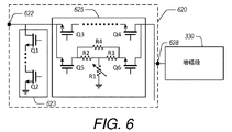
図6は、入力ポート622、帯域選択スイッチ623、減衰選択ブランチ625及び出力ポート628を有するマルチプレクサ例620を例示する。明確性を目的として、マルチプレクサ620を通る単数のブランチが例示されるが、図4を参照してここに詳述されたマルチプレクサを通る多数のスイッチ及びブランチも与えられて当該信号が共通出力部ポート628において出力され得ることを理解すべきである。入力ポート622から出力ポート628へと通る信号が、図3A及び図3Bを参照してここに詳述された増幅段330へと送信される。理解すべきことだが、マルチプレクサ620及び増幅段330は、図3A〜図5を参照してここに詳述されたように、制御器(図示せず)によって制御することができる。マルチプレクサ620は減衰選択ブランチ625を含むので、マルチプレクサ620はまた、図3A、図3B及び図4に関してここに詳述された減衰段320、420のような減衰段と称してもよい。
FIG. 6 illustrates a multiplexer example 620 having an
図6を参照すると、帯域選択スイッチ623により、マルチプレクサ620は、どの信号を増幅段330に伝えるのかを選択することができる。これは、信号を、目標の、選択された、又は所望の周波数帯域から選択するべく使用することができる。マルチプレクサ620における多数のブランチにより、対応する帯域選択スイッチ623を、処理を目的として目標の周波数帯域を選択するべく使用することができる。当該帯域選択スイッチ623は、任意の適切なパターンで(例えば時間に基づいて)又は制御器から受信した信号に基づいて、開閉することができる。このようにして、マルチプレクサ620及び増幅段330は、多重化された出力を与えるように構成される。帯域選択スイッチ623は、信号を選択的にグランド電位又は他の基準電圧に向けるべく構成されたトランジスタQ1、Q2を含む。帯域選択スイッチ623は、トランジスタQ1、Q2を動作させるのに適切なバイアス電圧を与えるべく、及び/又はインピーダンス整合素子若しくは他の信号調整素子を与えるべく、他のコンポーネントを含み得る。
With reference to FIG. 6, the
減衰選択ブランチ625は、可変減衰器R1を通る減衰経路、並びにトランジスタQ3及びQ4を通るバイパス経路を選択的に与えるべく構成される。減衰経路は、トランジスタQ5及びQ6により制御され、可変減衰器R1及び抵抗器R2〜R4を含む。抵抗器R2〜R4は、固定された抵抗値を有してよく、一定範囲の利得モードにわたる望ましい信号特性、信号振幅、及び/又はプログラムされた減衰を与えるべく選択してよい。可変減衰器R1は、動作利得モード、周波数帯域、信号振幅等に少なくとも部分的に依存する複数の値を有するように構成することができる。バイパス経路は、トランジスタQ3及びQ4により制御され、一定範囲の利得モードにわたる望ましい信号特性、信号振幅、及び/又はプログラムされた減衰を与えるべく付加的電気コンポーネント(図示せず)を含んでよい。いくつかの実施形態において、バイパス経路は高利得モードで動作するときに選択され、減衰経路は他の利得モードで動作するときに選択される。
The
マルチプレクサ620は、各ブランチに可変利得を有するマルチプレクサとして構成することができる。プログラム可能減衰部は、増幅段330に先立つスイッチング段又はスイッチングネットワークに設けることができる。このスイッチング段は、複数の減衰選択ブランチ625を含み得る。
The
図7は、減衰経路及びバイパス経路を与えるべく構成された増幅後減衰段例740を例示する。図3A及び図3Bを参照してここに詳述された増幅段330から受信した信号は、プログラム可能減衰器R1を使用して選択的に減衰させることができる。理解されることだが、増幅後減衰段740及び増幅段330は、図3A〜図5を参照してここに詳述された制御器(図示せず)によって制御することができる。増幅後減衰段740は、図3A、図3B及び図5に関してここに詳述された第2減衰段340、540として実装することができる。
FIG. 7 illustrates a post-amplification attenuation stage example 740 configured to provide an attenuation path and a bypass path. The signal received from the
図6を参照して記載した減衰選択ブランチ625と同様に、増幅後減衰段740は、可変減衰器R1を通る減衰経路並びにトランジスタQ3及びQ4を通るバイパス経路を選択的に与えるように構成される。減衰経路は、トランジスタQ5及びQ6により制御され、可変減衰器R1及び抵抗器R2〜R4を含む。抵抗器R2〜R4は、固定された抵抗値を有してよく、一定範囲の利得モードにわたる望ましい信号特性、信号振幅、及び/又はプログラムされた減衰を与えるべく選択してよい。可変減衰器R1は、動作利得モード、周波数帯域、信号振幅等に少なくとも部分的に依存する複数の値を有するように構成することができる。バイパス経路は、トランジスタQ3及びQ4により制御され、一定範囲の利得モードにわたる望ましい信号特性、信号振幅、及び/又はプログラムされた減衰を与えるべく付加的電気コンポーネント(図示せず)を含んでよい。いくつかの実施形態において、バイパス経路は高利得モードで動作するときに選択され、減衰経路は他の利得モードで動作するときに選択される。
Similar to the
図8A及び図8Bは、バイパスモード(図8A)及び減衰モード(図8B)において動作する減衰段740の一例を例示する。減衰段740は、図7を参照してここに記載される増幅後の段としてよく、又は図6を参照してここに記載される増幅前の段若しくはマルチプレクサにおけるブランチとしてもよい。図8Aに例示のバイパスモードにおいて、トランジスタQ3、Q4がアクティブになる一方、トランジスタQ5、Q6はアクティブ解除される。この構成において、信号は、減衰段740から出る前にトランジスタQ3、Q4間に設けられる電気コンポーネント(もしあれば)を通過する。図8Bに例示の減衰モードにおいて、トランジスタQ3、Q4がアクティブ解除される一方、トランジスタQ5、Q6はアクティブになる。この構成において信号は、減衰段740が存在する前に抵抗器R2〜R4及び可変減衰器R1を通過する。トランジスタをアクティブにし及びアクティブ解除することは、制御器(図示せず)によって制御することができる。可変減衰器R1の値は、制御器(図示せず)によって制御することができる。明確性を目的として図示しないにもかかわらず、減衰段740は、適切な制御信号及びバイアス電圧をトランジスタQ3〜Q6及び可変減衰器R1に与えるべく構成された他の電気コンポーネントを含み得る。
8A and 8B illustrate an example of
図9A及び図9Bは、可変利得増幅器例910a、910bを例示する。これは、増幅前減衰段620、各増幅段930a、930b、入力整合ネットワーク913、出力整合ネットワーク914及び増幅後減衰段740を含む。可変利得増幅器910a、910bは、複数の入力ポート912及び共通出力部ポート918を含む。増幅前減衰段620も、図6を参照してここに詳細に記載された減衰段又はマルチプレクサ620と同様に構成することができる。増幅後減衰段740は、図7を参照してここに詳述された減衰段740と同様に構成することができる。
9A and 9B illustrate examples of
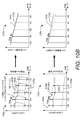
図9Aを参照すると、増幅段930aは、入力整合ネットワーク913を介して受信した信号を一緒になって増幅するトランジスタQ1、Q2、電圧源VDD、負荷ZL及びインダクタンス素子ZSを含むカスコード増幅器を含み得る。出力整合ネットワーク914は、望ましい信号特性を維持するべく増幅段930aのインピーダンスを整合するように構成されたコンポーネントを含む。例えば、出力整合ネットワーク913は、一つ以上のキャパシタ、一つ以上の抵抗器、直列の又は並列のキャパシタ又は抵抗器の組み合わせを含み得る。入力整合ネットワーク913は、望ましい信号特性を維持するべく第1減衰段920のインピーダンスを整合させるように構成されたコンポーネントを含む。例えば、入力整合ネットワーク914は、一つ以上のキャパシタ、一つ以上の抵抗器、直列の又は並列のキャパシタ又は抵抗器の組み合わせを含み得る。いくつかの実施形態において、入力整合ネットワーク913は、増幅段930aに含まれ得る。図9Bを参照すると、増幅段930bは増幅段930aと同様であり、付加的にデジェネレーションスイッチングブロック932を含む。デジェネレーションスイッチングブロック932は、第2インダクタンスZS1及びトランジスタQ3を含む。デジェネレーションスイッチングブロック932は、一つ以上の利得モードにおいて付加的インダクタンス素子ZS1を加えるように構成される。例えば、選択された利得モードにおいて、デジェネレーションスイッチングブロック932は、トランジスタQ3をアクティブ解除にしてグランド又は他の基準電圧への経路がインダクタンス素子ZS及びインダクタンス素子ZS1の双方を通過するようにできる。他の利得モードでは、デジェネレーションスイッチングブロック932は、トランジスタをアクティブにしてグランド又は他の基準電圧への経路がインダクタンス素子ZSを通過するがインダクタンス素子ZS1は通過しないようにできる。これにより、図10Bを参照してここに詳述されたように、増幅段930bの雑音指数(NF)及び/又は線形性(IIP3)に影響を与えることができる。
Referring to FIG. 9A, the
図10A及び図10Bは、図9A及び図9Bを参照してそれぞれが述べられた可変利得増幅器910a、910bの性能のプロットを例示する。図10Aは、(図9Aを参照して記載した)可変利得増幅器910aの雑音指数(NF)及び線形性(IIP3)と、記載の増幅前減衰段620を含むことの影響とのプロットを例示する。同様に、図10Bは、(図9Bを参照して記載した)可変利得増幅器910bの雑音指数(NF)及び線形性(IIP3)と、記載の増幅前減衰段620を含むことの影響とのプロットを例示する。
10A and 10B exemplify plots of performance of the
図10Aを参照すると、上部のプロットが、雑音指数(NF)を利得モードの関数として示す。G4が低利得モードであり、利得が高利得モードのG0に向かって増加する。左上のプロット1000aにおいて、増幅段930a(又はLNA)からのNFが実線1002aとして示され、NFはLNA前減衰段620なしでも存在する。目標NFは一点鎖線1004aとして示される。目標NF1004aとLNAからのNF1002aとの差は、破線1006a(例えばNFマージン)として示される許容LNA前減衰である。LNA前減衰段の可変減衰をプログラムすることにより、右上のプロット1010aに示されるように目標NFを達成することができる。LNA前減衰によるLNAからのNFが実線1012aとして示され、これが、一点鎖線1004aとして再び示される目標LNAに実質的に整合する。
Referring to FIG. 10A, the upper plot shows the noise figure (NF) as a function of gain mode. G4 is in the low gain mode, and the gain increases toward G0 in the high gain mode. In the upper
続けて図10Aを参照すると、下部のプロットが、線形性(IIP3)を利得モードの関数として示す。G4が低利得モードであり、利得が高利得モードのG0に向かって増加する。左下のプロット1020aにおいて、増幅段930a(又はLNA)からのIIP3が実線1022aとして示され、IIP3はLNA前減衰段620なしでも存在する。目標IIP3は一点鎖線1024aとして示される。許容LNA前減衰は再びであるが、破線1006aとして示される。LNA前減衰段の可変減衰をプログラムすることにより、プロット1030aに示すように、目標IIP3を超える線形性を達成することができる。LNA前減衰によるLNAからのIIP3が実線1032aとして示され、これが、一点鎖線1024aとして再び示される目標IIP3を超える。
Continuing with reference to FIG. 10A, the lower plot shows linearity (IIP3) as a function of gain mode. G4 is in the low gain mode, and the gain increases toward G0 in the high gain mode. In the lower
図10Aのプロットは、開示の可変利得増幅器が、非高利得モードにおいて目標の又は高いIIP3を達成するべく構成し得ることを例示する。さらに、許容NFマージンにより、低利得モードにおける線形性(IIP3)性能をブーストするべく目標のフロントエンド損失を達成するように、LNA前減衰をあつらえることができる。 The plot of FIG. 10A illustrates that the disclosed variable gain amplifier can be configured to achieve the target or high IIP3 in non-high gain mode. In addition, the permissible NF margin allows the LNA pre-damping to be tailored to achieve the target front-end loss to boost linearity (IIP3) performance in low gain mode.
図10Bに進むと、プロット1000、1010b、1020b、1030bが、図10Aに記載されるものと同じパラメータを例示する。増幅段930aが、デジェネレーションスイッチングブロック932を含む増幅段930bにより置換されている。換言すれば、可変利得増幅器910a、910b間の差が、可変利得増幅器910bにおけるデジェネレーションスイッチングブロック932の存在を含む。図10Bのプロットにおいて、スイッチングの影響は、NFプロット及びIIP3プロットにおける利得モードG3に対するデジェネレーションブロックに見られる。
Proceeding to FIG. 10B,
上部のプロットが、雑音指数(NF)を利得モードの関数として示す。G4が低利得モードであり、利得が高利得モードのG0に向かって増加する。左上のプロット1000bにおいて、増幅段930b(又はLNA)からのNFが実線1002bとして示され、NFはLNA前減衰段620なしでも存在する。目標NFは一点鎖線1004bとして示される。目標NF1004bとLNAからのNF1002bとの差は、破線1006b(例えばNFマージン)として示される許容LNA前減衰である。LNA前減衰段の可変減衰をプログラムすることにより、右上のプロット1010bに示されるように目標NFを達成することができる。LNA前減衰によるLNAからのNFが実線1012bとして示され、これが、一点鎖線1004bとして再び示される目標LNAに実質的に整合する。
The upper plot shows the noise figure (NF) as a function of gain mode. G4 is in the low gain mode, and the gain increases toward G0 in the high gain mode. In the upper
続けて図10Bを参照すると、下部のプロットが、線形性(IIP3)を利得モードの関数として示す。G4が低利得モードであり、利得が高利得モードのG0に向かって増加する。左下のプロット1020bにおいて、増幅段930b(又はLNA)からのIIP3が実線1022bとして示され、IIP3はLNA前減衰段620なしでも存在する。目標IIP3は一点鎖線1024bとして示される。許容LNA前減衰は再びであるが、破線1006bとして示される。LNA前減衰段の可変減衰をプログラムすることにより、プロット1030bに示すように、目標IIP3を超える線形性を達成することができる。LNA前減衰によるLNAからのIIP3が実線1032bとして示され、これが、一点鎖線1024bとして再び示される目標IIP3を超える。
Continuing with reference to FIG. 10B, the lower plot shows linearity (IIP3) as a function of gain mode. G4 is in the low gain mode, and the gain increases toward G0 in the high gain mode. In the lower left plot 1020b, IIP3 from
図10Bのプロットは、開示の可変利得増幅器が、非高利得モードにおいて目標の又は高いIIP3を達成するべく構成し得ることを例示する。さらに、許容NFマージンにより、低利得モードにおける線形性(IIP3)性能をブーストするべく目標のフロントエンド損失を達成するように、LNA前減衰をあつらえることができる。 The plot in FIG. 10B illustrates that the disclosed variable gain amplifier can be configured to achieve the target or high IIP3 in non-high gain mode. In addition, the permissible NF margin allows the LNA pre-damping to be tailored to achieve the target front-end loss to boost linearity (IIP3) performance in low gain mode.
製品及びアーキテクチャの複数例 Multiple examples of products and architectures
図11は、いくつかの実施形態において、特徴(例えば図1〜図9B)の組み合わせを有するダイバーシティ受信器構成のいくつか又はすべてを含むダイバーシティ受信器構成のいくつか又はすべてを、全体的又は部分的にモジュールに実装することができる。かかるモジュールは、例えばフロントエンドモジュール(FEM)とすることができる。かかるモジュールは、例えばダイバーシティ受信器(DRx)FEMとすることができる。かかるモジュールは、例えば、マルチ入力・マルチ出力(MiMo)モジュールとしてよい。 FIG. 11 shows, in some embodiments, some or all of the diversity receiver configurations including some or all of the features (eg, FIGS. 1-9B) in whole or in part. Can be implemented in a module. Such a module can be, for example, a front-end module (FEM). Such a module can be, for example, a diversity receiver (DRx) FEM. Such a module may be, for example, a multi-input / multi-output (MiMo) module.
図11の例において、モジュール1108はパッケージ基板1101を含み、かかるパッケージ基板1101に一定数のコンポーネントが取り付けられる。例えば、(フロントエンド電力管理集積回路[FE−PIMC]を含み得る)制御器1102、組み合わせアセンブリ1106、ここに記載される一つ以上の特徴を有する埋め込み型プログラム可能減衰器1116を含む可変利得増幅器アセンブリ1110、及び(一つ以上の帯域通過フィルタを含み得る)フィルタバンク1108を、パッケージ基板1101上に及び/又はパッケージ基板1101内に取り付け及び/又は実装することができる。一定数のSMTデバイス1105のような他のコンポーネントを、パッケージ基板1101に取り付けることもできる。様々なコンポーネントのすべてがパッケージ基板1101上にレイアウトされるように描かれているにもかかわらず、一定のコンポーネントを他のコンポーネントの上に実装することもできることが理解される。
In the example of FIG. 11, the
いくつかの実施形態において、ダイバーシティ受信モジュール1108は、2つ以上の可変利得増幅器アセンブリ1110を含む。様々な実装において、2つ以上の可変利得増幅器アセンブリ1110は、単数のダイ上に実装することができる。各アセンブリ1110は、第1減衰段、増幅段及び第2減衰段を含み得る。各アセンブリ1110の出力が一緒にされる。これは、広い範囲の周波数にわたる性能チューニングが可能となるので有利となり得る。例えば、第1アセンブリを第1周波数範囲のためにチューニングすることができ、第2アセンブリを第2周波数範囲のためにチューニングすることができる。複数の信号が、適切なアセンブリ1110へと向けられて共通出力部において一緒になる。すなわち、ダイバーシティ受信モジュール1108は、広い範囲の周波数をカバーするように構成することができるので、単数の増幅器アセンブリを含む構成と比べて性能が改善される。
In some embodiments, the
図12は、いくつかの実施形態において、複数の特徴(例えば図1〜図9b)の組み合わせを有するダイバーシティ受信器構成のいくつか又はすべてを含むダイバーシティ受信器構成のいくつか又はすべてを、全体的に又は部分的に、アーキテクチャに実装することができることを示す。かかるアーキテクチャは、一つ以上のモジュールを含み、ダイバーシティ受信器(DRx)フロントエンド機能のようなフロントエンド機能を与えるように構成することができる。 FIG. 12 shows, in some embodiments, some or all of the diversity receiver configurations including some or all of the diversity receiver configurations having a combination of multiple features (eg, FIGS. 1-9b) as a whole. Indicates that it can be implemented in the architecture, either or partially. Such an architecture may include one or more modules and be configured to provide front-end functionality such as diversity receiver (DRx) front-end functionality.
図12の例において、アーキテクチャ1208は、(フロントエンド電力管理集積回路[FE−PIMC]を含み得る)制御器1202、組み合わせアセンブリ1206、ここに記載される一つ以上の特徴を有する埋め込み型プログラム可能減衰器1216を含む可変利得増幅器アセンブリ1210、及び(一つ以上の帯域通過フィルタを含み得る)フィルタバンク1208を、パッケージ基板1201上に及び/又はパッケージ基板1201内に取り付け及び/又は実装することができる。一定数のSMTデバイス1205のような他のコンポーネントもまた、アーキテクチャ1208に実装することができる。
In the example of FIG. 12,
いくつかの実装において、ここに記載される一つ以上の特徴を有するデバイス及び/又は回路は、無線デバイスのようなRF電子デバイスに含まれ得る。かかるデバイス及び/又は回路は、無線デバイスに直接、ここに記載されるモジュラー形態で、又はこれらの何らかの組み合わせで実装することができる。いくつかの実施形態において、かかる無線デバイスは、例えば、スマートフォンのような携帯電話機、電話機能あり又はなしのハンドヘルド無線デバイス、無線タブレット等を含み得る。 In some implementations, devices and / or circuits having one or more features described herein may be included in RF electronic devices such as wireless devices. Such devices and / or circuits can be implemented directly on the wireless device in the modular form described herein, or in any combination thereof. In some embodiments, such wireless devices may include, for example, mobile phones such as smartphones, handheld wireless devices with or without telephone capabilities, wireless tablets and the like.
図13は、ここに記載される一つ以上の有利な特徴を有する無線デバイス例1300を描く。ここに記載される一つ以上の特徴を有する一つ以上のモジュールの文脈において、かかるモジュールは一般に、(例えばフロントエンドモジュールとして実装可能な)破線の囲い1306、及び(例えばフロントエンドモジュールとして実装可能な)ダイバーシティ受信器(DRx)モジュール1308によって描かれる。
FIG. 13 depicts an
図13を参照すると、複数の電力増幅器(PA)1382がそれぞれ、送受信器1304からRF信号を受信することができる。送受信器1304は、増幅及び送信対象のRF信号を生成するように、及び受信信号を処理するように、構成されて動作することができる。送受信器1304は、ユーザに適したデータ及び/又は音声信号と送受信器1304に適したRF信号との間の変換を与えるように構成されたベース帯域サブシステム1305と相互作用をするように示される。送受信器1304はまた、無線デバイス1300の動作を目的として電力を管理するべく構成された電力管理コンポーネント1307と通信することもできる。かかる電力管理はまた、ベース帯域サブシステム1305並びにモジュール1306及び1308の動作も制御することができる。
With reference to FIG. 13, each of the plurality of power amplifiers (PAs) 1382 can receive RF signals from the transmitter /
ベース帯域サブシステム1305は、ユーザに与えられ及びユーザから受信する音声及び/又はデータの様々な入力及び出力を容易にするべくユーザインタフェイス1301に接続されるように示される。ベース帯域サブシステム1305はまた、無線デバイスの動作を容易にするべく及び/又はユーザのための情報格納を与えるべく構成されたメモリ1303にも接続される。メモリ1303は、データ及び/又は命令を格納するように構成される。
The
無線デバイス例1300において、PA1382の出力は、(各整合回路1384を介して)整合されて各デュプレクサ1386へと引き回される。かかる増幅されかつフィルタリングされた信号は、送信を目的としてスイッチングネットワーク1309を介して一次アンテナ1360へと引き回すことができる。いくつかの実施形態において、デュプレクサ1386により、共通アンテナ(例えば一次アンテナ1360)を使用して送信動作及び受信動作を同時に行うことが許容され得る。図13において、受信信号は、ここに開示の可変利得増幅器の特徴及び利益を与える可変利得増幅器アセンブリ1310aへと引き回されるように示される。DRxモジュール1308も、同様の可変利得増幅器アセンブリ1310bを含む。
In wireless device example 1300, the output of PA1382 is matched (via each matching circuit 1384) and routed to each
無線デバイス例1300において、一次アンテナ1330において受信した信号は、(各整合回路1385を介して)整合され、フロントエンドモジュール1306の可変利得増幅器1310aに送信され得る。可変利得増幅器1310aは、増幅前プログラム可能減衰アセンブリ1320、増幅器1330、増幅後プログラム可能減衰アセンブリ1340、及び分割器1350を含み得る。可変利得増幅器1310aは、入力部1312において複数の信号を受信し、出力部1318において複数の処理済み信号を出力するように構成される。可変利得増幅器1310aは、複数のスイッチング可能経路を増幅器1310aに与えるべく構成される。複数のスイッチング可能経路は、複数の利得モードにわたる目標の増幅を与えるとともに、埋め込み型プログラム可能減衰器を含まない可変利得増幅器と比べて信号の線形性を改善する埋め込み型プログラム可能減衰器を含む。少なくとも一つの高利得モードにおいて、プログラム可能減衰器は、雑音指数への影響を低減又は排除するべくバイパスすることができる。少なくとも一つの非高利得モードにおいて、プログラム可能減衰器は、当該少なくとも一つの非高利得モードにおいて増幅される信号の線形性を改善するようにあつらえることができる。
In wireless device example 1300, the signal received by the
無線デバイスはまた、ダイバーシティアンテナ1370、及びダイバーシティアンテナ1370から信号を受信するダイバーシティ受信器モジュール1308も含む。ダイバーシティ受信モジュール1308は、フロントエンドモジュール1306における可変利得増幅器1310aと同様の可変利得増幅器1310bを含む。ダイバーシティ受信器モジュール1308及び可変利得増幅器1310bは、受信した信号を処理し、処理した信号を送受信器1304に送信する。いくつかの実施形態において、ダイプレクサ、トライプレクサ、又は他のマルチプレクサ若しくはフィルタアセンブリを、ここに記載されるように、ダイバーシティアンテナ1370とダイバーシティ受信器モジュール1308との間に含めることができる。
The wireless device also includes a
本開示の一つ以上の特徴を、ここに記載される様々なセルラー周波数帯域とともに実装することができる。かかる帯域の例を表1に挙げる。理解されることだが、当該帯域の少なくともいくつかは、サブ帯域に分割することができる。本開示の一つ以上の特徴が、表1の例のような指定を有しない周波数範囲とともに実装し得ることも理解される。無線周波数(RF)及び無線周波数信号との用語が、少なくとも表1に挙げられる周波数を含む信号を言及することが理解される。

本開示は、様々な特徴を記載するが、その単一の特徴のみがここに記載される利益に対する責任を負うわけではない。理解されることだが、ここに記載される様々な特徴は、当業者にとって明らかなように結合し、修正し、又は省略することができる。ここに具体的に記載されるもの以外のコンビネーション及びサブコンビネーションも、当業者にとって明らかであって、本開示の一部を形成することが意図される。様々な方法が、様々なフローチャートステップ及び/又はフェーズに関連してここに記載される。理解されることだが、多くの場合、一定のステップ及び/又はフェーズは、フローチャートに示される多重のステップ及び/又はフェーズが単数のステップ及び/又はフェーズとして行うことができるように、一緒に組み合わせることができる。さらに、一定のステップ及び/又はフェーズは、別個に行うべく付加的な下位コンポーネントに分解することもできる。いくつかの例において、ステップ及び/又はフェーズの順序は再配列することができ、一定のステップ及び/又はフェーズを完全に省略することもできる。さらに、ここに記載される方法は、ここに図示され及び記載されるものに対する付加的なステップ及び/又はフェーズも行うことができるような、オープンエンドとして理解される。 The present disclosure describes various features, but not only that single feature is liable for the benefits described herein. As will be appreciated, the various features described herein can be combined, modified or omitted as will be apparent to those skilled in the art. Combinations and sub-combinations other than those specifically described herein are also apparent to those skilled in the art and are intended to form part of the present disclosure. Various methods are described herein in connection with various flowchart steps and / or phases. It is understood that, in many cases, certain steps and / or phases are combined together so that the multiple steps and / or phases shown in the flow chart can be performed as a single step and / or phase. Can be done. In addition, certain steps and / or phases can be broken down into additional subcomponents to be done separately. In some examples, the order of steps and / or phases can be rearranged and certain steps and / or phases can be omitted altogether. Further, the methods described herein are understood as open-ended so that additional steps and / or phases to those illustrated and described herein can also be performed.
ここに記載されるシステム及び方法のいくつかの態様は有利なことに、例えば、コンピュータソフトウェア、ハードウェア、ファームウェア、又は、コンピュータソフトウェア、ハードウェア及びファームウェアの任意の組み合わせを使用して実装可能である。コンピュータソフトウェアは、実行時にここに記載の機能を行う、コンピュータ可読媒体(例えば非一時的コンピュータ可読媒体)に記憶されたコンピュータ実行可能コードを含み得る。いくつかの実施形態において、コンピュータ実行可能コードは、一つ以上の汎用コンピュータプロセッサによって実行される。当業者であれば、本開示に照らし、汎用コンピュータにおいて実行されるソフトウェアを使用して実装可能な任意の特徴又は機能が、ハードウェア、ソフトウェア又はファームウェアの異なる組み合わせを使用しても実装可能であることがわかる。例えば、かかるモジュールは、集積回路の組み合わせを使用して完全にハードウェアに実装することができる。代替的に又は付加的に、かかる特徴又は機能は、汎用コンピュータによらず、ここに記載される特定の機能を実行するべく設計された専用コンピュータを使用して完全に又は部分的に実装可能である。 Some aspects of the systems and methods described herein are advantageously implemented using, for example, computer software, hardware, firmware, or any combination of computer software, hardware and firmware. .. Computer software may include computer-executable code stored on a computer-readable medium (eg, a non-transitory computer-readable medium) that performs the functions described herein at run time. In some embodiments, the computer executable code is executed by one or more general purpose computer processors. Any person skilled in the art can implement any feature or function that can be implemented using software running on a general purpose computer in the light of the present disclosure, using different combinations of hardware, software or firmware. You can see that. For example, such modules can be fully implemented in hardware using a combination of integrated circuits. Alternatively or additionally, such features or functions may be fully or partially implemented using a dedicated computer designed to perform the particular function described herein, regardless of a general purpose computer. is there.
多重分散されたコンピューティング装置を、ここに記載される任意の一つのコンピューティングデバイスの代わりに用いることができる。かかる分散された実施形態において、分散されたコンピューティングデバイスのそれぞれにおいていくつかの機能が行われるように、一つのコンピューティングデバイスの機能が(例えばネットワークを介して)分散される。 Multiple distributed computing devices can be used in place of any one of the computing devices described herein. In such a distributed embodiment, the functionality of one computing device is distributed (eg, over a network) so that some functionality is performed on each of the distributed computing devices.
いくつかの実施形態は、式、アルゴリズム、及び/又はフローチャートの例示を参照して記載することができる。当該方法は、一つ以上のコンピュータにおいて実行可能なコンピュータプログラム命令を使用して実装することができる。当該方法はまた、別個に又は装置若しくはシステムの一コンポーネントとしてのいずれかでコンピュータプログラム製品として実装することができる。この点において、式、アルゴリズム、ブロック、又はフローチャートのステップ、及びこれらの組み合わせのそれぞれを、コンピュータ可読プログラムコード論理に具体化された一つ以上のコンピュータプログラム命令を含むハードウェア、ファームウェア及び/又はソフトウェアによって実装することができる。わかることだが、かかるコンピュータプログラム命令はいずれも、コンピュータ又は他のプログラム可能処理デバイスにおいて実行されるコンピュータプログラム命令が、式、アルゴリズム及び/又はフローチャートに特定される機能を実装するように、制約なしに汎用コンピュータ若しくは専用コンピュータ、又は機械をもたらす他のプログラム可能処理装置を含む一つ以上のコンピュータにロードすることができる。またも理解されることだが、式、アルゴリズム、及び/又はフローチャートのブロックの例示、並びにこれらの組み合わせのそれぞれは、特定の機能若しくはステップ、又は、専用ハードウェアとコンピュータ可読プログラムコード論理手段との組み合わせを行う専用ハードウェア系コンピュータシステムによって実装することができる。 Some embodiments can be described with reference to examples of equations, algorithms, and / or flowcharts. The method can be implemented using computer program instructions that can be executed on one or more computers. The method can also be implemented as a computer program product, either separately or as a component of a device or system. In this regard, hardware, firmware and / or software containing one or more computer program instructions embodied in computer-readable program code logic, each of an expression, algorithm, block, or flowchart step, and a combination thereof. Can be implemented by. As you can see, any such computer program instruction is unconstrained so that the computer program instruction executed on the computer or other programmable processing device implements the functions specified in the expressions, algorithms and / or flowcharts. It can be loaded into a general purpose computer or a dedicated computer, or one or more computers including other programmable processing devices that bring the machine. As will also be understood, examples of blocks of expressions, algorithms, and / or flowcharts, and each of these combinations, are specific functions or steps, or combinations of dedicated hardware and computer-readable program code logic means. It can be implemented by a dedicated hardware computer system.
さらに、コンピュータ可読プログラムコード論理に具体化されるコンピュータプログラム命令はまた、コンピュータ可読メモリ(例えば非一時的コンピュータ可読媒体)に記憶させることができる。当該コンピュータ可読メモリは、コンピュータ可読メモリに記憶された命令がフローチャート(複数可)のブロック(複数可)に特定された機能(複数可)を実装するように、一つ以上のコンピュータ又は他のプログラム可能処理デバイスを特定の態様で機能させることができる。コンピュータプログラム命令はまた、一つ以上のコンピュータ又は他のプログラム可能コンピューティングデバイスにロードされて当該一以上のコンピュータ又は他のプログラム可能コンピューティングデバイスにおいて一連の動作ステップを実行させることにより、当該コンピュータ又は他のプログラム可能処理装置において実行される命令が、式、アルゴリズム、及び/又はフローチャートブロックに特定される機能を実装するためのステップを与えるようにコンピュータ実装プロセスをもたらすことができる。 Further, computer program instructions embodied in computer-readable program code logic can also be stored in computer-readable memory (eg, non-temporary computer-readable media). The computer-readable memory is one or more computers or other programs so that the instructions stored in the computer-readable memory implement the function (s) specified in the block (s) of the flowchart (s). Possible processing devices can be made to function in a particular manner. Computer program instructions are also loaded onto one or more computers or other programmable computing devices to perform a series of operating steps on the one or more computers or other programmable computing devices. Instructions executed in other programmable processors can result in a computer-implemented process to provide steps for implementing the functions specified in expressions, algorithms, and / or flowchart blocks.
ここに記載される方法及びタスクのいくつか又はすべては、コンピュータシステムによって行われ及び完全に自動化することができる。コンピュータシステムは、いくつかの場合において、記載の機能を行うべくネットワークを介して通信し及び相互運用される多数の別個のコンピュータ又はコンピューティングデバイス(例えば物理的サーバ、ワークステーション、記憶アレイ等)を含み得る。かかるコンピューティングデバイスはそれぞれが典型的に、メモリ又は他の非一時的コンピュータ可読記憶媒体若しくは装置に記憶されたプログラム命令又はモジュールを実行するプロセッサ(又は多重プロセッサ)を含む。ここに開示の様々な機能は、かかるプログラム命令に具体化することができる。ただし、代替的に、開示の機能のいくつか又はすべてを、コンピュータシステムの特定用途向け回路(例えばASIC又はFPGA)に実装してよい。コンピュータシステムが多数のコンピューティングデバイスを含む場合、当該デバイスは共通位置に配置してよいが、必ずしもその必要はない。開示の方法及びタスクの結果は、半導体メモリチップ及び/又は磁気ディスクのような物理的記憶デバイスを異なる状態に変換することよって永続的に記憶することができる。 Some or all of the methods and tasks described herein can be performed by computer systems and fully automated. A computer system, in some cases, has a large number of separate computers or computing devices (eg, physical servers, workstations, storage arrays, etc.) that communicate and interoperate over a network to perform the described functions. Can include. Each such computing device typically includes a processor (or multiple processor) that executes a program instruction or module stored in memory or other non-temporary computer-readable storage medium or device. The various functions disclosed herein can be embodied in such program instructions. However, instead, some or all of the disclosed functions may be implemented in application specific circuits (eg, ASICs or FPGAs) in computer systems. If the computer system includes a large number of computing devices, the devices may, but are not necessarily, co-located. The results of the disclosed methods and tasks can be permanently stored by converting physical storage devices such as semiconductor memory chips and / or magnetic disks into different states.
本明細書及び特許請求の範囲全体にわたり、文脈上そうでないことが明らかでない限り、「含む」等の用語は、排他的又は網羅的な意味とは反対の包括的意味に、すなわち「〜を含むがこれらに限られない」との意味に解釈すべきである。ここで一般に使用される用語「結合」は、直接接続されるか又は一つ以上の中間要素を介して接続されるかいずれかとなり得る2つ以上の要素を言及する。加えて、用語「ここ」、「上」、「下」及び同様の趣旨の用語は、本願において使用される場合、本願全体を言及し、本願の任意の特定部分を言及するわけではない。文脈が許容する場合、単数又は複数を使用する上述の詳細な説明における用語はそれぞれ、複数又は単数をも含み得る。2つ以上の項目のリストを参照する用語「又は」及び「若しくは」について、当該用語は以下の解釈のすべてをカバーする。すなわち、当該リストの任意の項目、当該リストのすべての項目、及び当該リストの項目の任意の組み合わせである。用語「代表的」は、ここでは専ら「一例又は一例示として機能する」ことを意味するべく使用される。「代表的」としてここに記載される任意の実装は必ずしも、他の実装に対して好ましい又は有利として解釈されるわけではない。 Throughout the present specification and claims, terms such as "including" have an inclusive meaning as opposed to an exclusive or exhaustive meaning, i.e., "including," unless it is clear in the context that this is not the case. Is not limited to these. " The term "combination" commonly used herein refers to two or more elements that can be either directly connected or connected via one or more intermediate elements. In addition, the terms "here", "above", "below" and similar to the same meaning, when used herein, refer to the entire application and not any particular part of the application. Where the context allows, the terms in the above detailed description using the singular or plural may also include the plural or singular, respectively. For terms "or" and "or" that refer to a list of two or more items, the term covers all of the following interpretations. That is, any item in the list, all items in the list, and any combination of items in the list. The term "representative" is used herein exclusively to mean "acting as an example or an example." Any implementation described herein as "representative" is not necessarily construed as favorable or advantageous over other implementations.
本開示は、ここに示される実装に制限されることを意図しない。本開示に記載される実装に対する様々な修正は、当業者にとって容易にわかるものであり、ここに画定される一般的な原理は、本開示の要旨又は範囲を逸脱することなく他の実装に対しても適用することができる。ここに与えられる本発明の教示は、他の方法及びシステムに対しても適用可能であり、上述の方法及びシステムに制限されるわけではなく、上述の様々な実施形態の要素及び行為は、さらなる実施形態を与えるべく組み合わせることができる。したがって、ここに記載される新規な方法及びシステムは、様々な他の形態で具体化することができる。さらに、ここに記載される方法及びシステムの形態における様々な省略、置換及び変更が、本開示の要旨から逸脱することなくなし得る。添付の特許請求の範囲及びその均等物が、本開示の範囲及び要旨に収まるかかる形態又は修正をカバーすることが意図される。
This disclosure is not intended to be limited to the implementations presented herein. Various modifications to the implementations described in this disclosure will be readily apparent to those of skill in the art, and the general principles defined herein will relate to other implementations without departing from the gist or scope of this disclosure. Can also be applied. The teachings of the present invention given herein are also applicable to other methods and systems and are not limited to the methods and systems described above, and the elements and actions of the various embodiments described above are further described. Can be combined to give embodiments. Therefore, the novel methods and systems described herein can be embodied in various other forms. Moreover, various omissions, substitutions and changes in the methods and forms of the system described herein may be made without departing from the gist of the present disclosure. It is intended that the appended claims and their equivalents cover such forms or modifications that fall within the scope and gist of the present disclosure.
Claims (20)
各ブランチが複数のスイッチ回路及び一の可変減衰素子を含む複数のブランチを有する第1減衰段であって、共通出力部及び各ブランチ用の入力部を含む第1減衰段と、
多重化された出力を与えるべく前記第1減衰段の共通出力部に結合された増幅段と、
一定範囲の利得レベルにわたって様々な所望の特性を維持する増幅された出力信号を与えるべく、前記増幅段の多重化された出力を受信するように構成された第2減衰段と
を含み、
前記複数のブランチのうち少なくとも一つのブランチは、
少なくとも一つのスイッチ回路を含む第1の経路と、
2つのスイッチ回路と、前記2つのスイッチ回路の間に直列に接続された前記可変減衰素子とを含む第2の経路と
を含み、
前記第1減衰段は前記複数のスイッチ回路の動作により、信号が前記第1の経路を通過する第1状態において前記可変減衰素子をバイパスする経路を与え、信号が前記第2の経路を通過する第2状態において前記可変減衰素子を通過する経路を与え、信号が前記第1の経路及び前記第2の経路の双方を通過しない第3状態において前記少なくとも一つのブランチを通過するいずれの信号も排除するように構成される増幅器。 Variable gain signal amplifier
A first attenuation stage in which each branch has a plurality of branches including a plurality of switch circuits and one variable attenuation element, and a first attenuation stage including a common output unit and an input unit for each branch.
An amplification stage coupled to the common output section of the first attenuation stage to provide multiplexed output,
It includes a second attenuation stage configured to receive the multiplexed output of the amplification stage to provide an amplified output signal that maintains a variety of desired characteristics over a range of gain levels.
At least one of the plurality of branches
A first path that includes at least one switch circuit,
A second path including the two switch circuits and the variable damping element connected in series between the two switch circuits.
Including
The first attenuation stage provides a path for bypassing the variable attenuation element in the first state in which the signal passes through the first path by the operation of the plurality of switch circuits, and the signal passes through the second path. A path is provided through the variable attenuation element in the second state, and any signal passing through the at least one branch in the third state where the signal does not pass through both the first path and the second path is excluded. An amplifier configured to do.
可変利得信号増幅器と、
前記可変利得信号増幅器の複数の選択入力に周波数帯域を向けるべく前記可変利得信号増幅器に結合されたフィルタアセンブリと、
複数の利得モードを与えるべく前記可変利得信号増幅器を制御するように実装された制御器と
を含み、
前記可変利得信号増幅器は、
各ブランチが複数のスイッチ回路及び一の可変減衰素子を含む複数のブランチを有する第1減衰段であって、共通出力部及び各ブランチ用の入力部を有する第1減衰段と、
多重化された出力を与えるべく前記第1減衰段の共通出力部に結合された増幅段と、
一定範囲の利得レベルにわたって様々な所望の特性を維持する増幅された出力信号を与えるべく前記増幅段の多重化された出力を受信するように構成された第2減衰段と
を含み、
前記複数のブランチのうち少なくとも一つのブランチは、
少なくとも一つのスイッチ回路を含む第1の経路と、
2つのスイッチ回路と、前記2つのスイッチ回路の間に直列に接続された前記可変減衰素子とを含む第2の経路と
を含み、
前記第1減衰段は前記複数のスイッチ回路の動作により、信号が前記第1の経路を通過する第1状態において前記可変減衰素子をバイパスする経路を与え、信号が前記第2の経路を通過する第2状態において前記可変減衰素子を通過する経路を与え、信号が前記第1の経路及び前記第2の経路の双方を通過しない第3状態において前記少なくとも一つのブランチを通過するいずれの信号も排除するように構成され、
高利得モードにおいて、前記可変利得信号増幅器は、特定のブランチにおける前記可変減衰素子を、前記特定のブランチにおけるスイッチ回路を前記第1状態となるように制御することによってバイパスする経路に沿うように信号を出力するフロントエンドアーキテクチャ。 Front-end architecture
Variable gain signal amplifier and
A filter assembly coupled to the variable gain signal amplifier to direct the frequency band to a plurality of selective inputs of the variable gain signal amplifier.
Including a controller implemented to control the variable gain signal amplifier to provide multiple gain modes.
The variable gain signal amplifier
A first attenuation stage in which each branch has a plurality of branches including a plurality of switch circuits and one variable attenuation element, and a first attenuation stage having a common output unit and an input unit for each branch.
An amplification stage coupled to the common output section of the first attenuation stage to provide multiplexed output,
It includes a second attenuation stage configured to receive the multiplexed output of the amplification stage to provide an amplified output signal that maintains a variety of desired characteristics over a range of gain levels.
At least one of the plurality of branches
A first path that includes at least one switch circuit,
A second path including the two switch circuits and the variable damping element connected in series between the two switch circuits.
Including
The first attenuation stage provides a path for bypassing the variable attenuation element in the first state in which the signal passes through the first path by the operation of the plurality of switch circuits, and the signal passes through the second path. A path is provided through the variable attenuation element in the second state, and any signal passing through the at least one branch in the third state where the signal does not pass through both the first path and the second path is excluded. Configured to
In high gain mode, the variable gain signal amplifier signals along a path that bypasses the variable attenuation element in a particular branch by controlling the switch circuit in the particular branch to be in the first state. front-end architecture you output.
ダイバーシティアンテナと、
信号を受信して選択経路に沿うように周波数帯域を向けるべく前記ダイバーシティアンテナに結合されたフィルタアセンブリと、
選択経路から信号を受信するべく前記フィルタアセンブリに結合された可変利得信号増幅器と、
複数の利得モードを与えるべく前記可変利得信号増幅器を制御するように実装された制御器と
を含み、
前記可変利得信号増幅器は、
各ブランチが複数のスイッチ回路及び一の可変減衰素子を含む複数のブランチを有する第1減衰段であって、共通出力部及び各ブランチ用の入力部を含む第1減衰段と、
多重化された出力を与えるべく前記第1減衰段の共通出力部に結合された増幅段と、
一定範囲の利得レベルにわたって様々な所望の特性を維持する増幅された出力信号を与えるべく前記増幅段の多重化された出力を受信するように構成された第2減衰段と
を含み、
前記複数のブランチのうち少なくとも一つのブランチは、
少なくとも一つのスイッチ回路を含む第1の経路と、
2つのスイッチ回路と、前記2つのスイッチ回路の間に直列に接続された前記可変減衰素子とを含む第2の経路と
を含み、
前記第1減衰段は前記複数のスイッチ回路の動作により、信号が前記第1の経路を通過する第1状態において前記可変減衰素子をバイパスする経路を与え、信号が前記第2の経路を通過する第2状態において前記可変減衰素子を通過する経路を与え、信号が前記第1の経路及び前記第2の経路の双方を通過しない第3状態において前記少なくとも一つのブランチを通過するいずれの信号も排除するように構成され、
高利得モードにおいて、前記可変利得信号増幅器が、特定のブランチにおいて前記可変減衰素子を、前記特定のブランチにおけるスイッチ回路を前記第1状態となるように制御することによってバイパスする経路に沿うように信号を出力するデバイス。 It ’s a wireless device,
Diversity antenna and
A filter assembly coupled to the diversity antenna to receive the signal and direct the frequency band along the selected path.
A variable gain signal amplifier coupled to the filter assembly to receive a signal from the selected path,
Including a controller implemented to control the variable gain signal amplifier to provide multiple gain modes.
The variable gain signal amplifier
A first attenuation stage in which each branch has a plurality of branches including a plurality of switch circuits and one variable attenuation element, and a first attenuation stage including a common output unit and an input unit for each branch.
An amplification stage coupled to the common output section of the first attenuation stage to provide multiplexed output,
It includes a second attenuation stage configured to receive the multiplexed output of the amplification stage to provide an amplified output signal that maintains a variety of desired characteristics over a range of gain levels.
At least one of the plurality of branches
A first path that includes at least one switch circuit,
A second path including the two switch circuits and the variable damping element connected in series between the two switch circuits.
Including
The first attenuation stage provides a path for bypassing the variable attenuation element in the first state in which the signal passes through the first path by the operation of the plurality of switch circuits, and the signal passes through the second path. A path is provided through the variable attenuation element in the second state, and any signal passing through the at least one branch in the third state where the signal does not pass through both the first path and the second path is excluded. Configured to
In high gain mode, the variable gain signal amplifier signals along a path that bypasses the variable attenuation element in a particular branch by controlling the switch circuit in the particular branch to be in the first state. devices that output.
Applications Claiming Priority (3)
| Application Number | Priority Date | Filing Date | Title |
|---|---|---|---|
| US201662381262P | 2016-08-30 | 2016-08-30 | |
| US62/381,262 | 2016-08-30 | ||
| PCT/US2017/049324 WO2018045002A1 (en) | 2016-08-30 | 2017-08-30 | Multi-input amplifier with programmable embedded attenuators |
Publications (3)
| Publication Number | Publication Date |
|---|---|
| JP2019525692A JP2019525692A (en) | 2019-09-05 |
| JP2019525692A5 JP2019525692A5 (en) | 2020-10-08 |
| JP6853362B2 true JP6853362B2 (en) | 2021-03-31 |
Family
ID=61243617
Family Applications (1)
| Application Number | Title | Priority Date | Filing Date |
|---|---|---|---|
| JP2019531585A Active JP6853362B2 (en) | 2016-08-30 | 2017-08-30 | Variable gain signal amplifier, front-end architecture and wireless devices |
Country Status (9)
| Country | Link |
|---|---|
| US (3) | US10348262B2 (en) |
| JP (1) | JP6853362B2 (en) |
| KR (2) | KR20230107705A (en) |
| CN (1) | CN109891742B (en) |
| DE (1) | DE112017004355T8 (en) |
| GB (3) | GB2605112B (en) |
| SG (2) | SG11201901804PA (en) |
| TW (3) | TWI811976B (en) |
| WO (1) | WO2018045002A1 (en) |
Families Citing this family (22)
| Publication number | Priority date | Publication date | Assignee | Title |
|---|---|---|---|---|
| EP4024939A1 (en) | 2014-08-18 | 2022-07-06 | Panasonic Holdings Corporation | Mimo training method and radio device |
| GB2605112B (en) * | 2016-08-30 | 2023-01-11 | Skyworks Solutions Inc | Multi-input amplifier with programmable embedded attenuators |
| US20180091108A1 (en) * | 2016-09-28 | 2018-03-29 | Qualcomm Incorporated | Optimization for energy efficient multi-channel communication with shared lna structure |
| FR3065339B1 (en) * | 2017-04-13 | 2019-07-05 | Stmicroelectronics Sa | TRANSMISSION LINE WITH DEVICE FOR LIMITING LOSSES BY DISAPPOINTMENT |
| JP7148056B2 (en) * | 2018-05-08 | 2022-10-05 | 日清紡マイクロデバイス株式会社 | variable gain amplifier |
| US10496587B1 (en) * | 2018-06-27 | 2019-12-03 | Integrated Device Technology, Inc. | Wide programmable gain receiver data path for single-ended memory interface application |
| JP6937272B2 (en) * | 2018-06-29 | 2021-09-22 | 株式会社東芝 | High frequency amplifier circuit |
| CN110798266A (en) * | 2018-08-03 | 2020-02-14 | 上海欣诺通信技术股份有限公司 | Light splitting device and computer storage medium |
| US10700650B1 (en) * | 2019-01-08 | 2020-06-30 | Psemi Corporation | Configurable wideband split LNA |
| US10951252B2 (en) | 2019-01-08 | 2021-03-16 | Psemi Corporation | 5G NR configurable wideband RF front-end LNA |
| CN113366759A (en) | 2019-01-08 | 2021-09-07 | 派赛公司 | Configurable wideband split LNA |
| US11469725B2 (en) | 2019-06-07 | 2022-10-11 | Skyworks Solutions, Inc. | Apparatus and methods for power amplifier output matching |
| US11239803B2 (en) * | 2019-09-17 | 2022-02-01 | Psemi Corporation | Ruggedness protection circuit |
| US11159130B2 (en) | 2019-09-17 | 2021-10-26 | Psemi Corporation | Ruggedness protection circuit |
| KR20210033090A (en) * | 2019-09-17 | 2021-03-26 | 한국전자통신연구원 | Microwave amplification circuit |
| CN110658443B (en) * | 2019-10-21 | 2021-03-26 | 浙江大学 | Aging system for radio frequency front-end device |
| US11218123B2 (en) | 2020-03-12 | 2022-01-04 | Texas Instruments Incorporated | Chopper stabilized attenuation for sense amplifiers |
| KR102540949B1 (en) | 2021-09-17 | 2023-06-07 | 주식회사 퀄리타스반도체 | A signal processing circuit improving linearity of pulse amplitude modulated signal and communication device including the circuit |
| CN114189222A (en) * | 2021-12-20 | 2022-03-15 | 上海迦美信芯通讯技术有限公司 | Multi-gain control low noise amplifier with improved phase jump |
| CN115441839A (en) * | 2022-09-16 | 2022-12-06 | 深圳飞骧科技股份有限公司 | Multi-band low noise amplifier, integrated circuit chip and electronic device |
| CN115208338A (en) * | 2022-09-16 | 2022-10-18 | 深圳飞骧科技股份有限公司 | Multi-band low noise amplifier and communication equipment |
| CN115296620B (en) * | 2022-09-29 | 2022-12-30 | 深圳飞骧科技股份有限公司 | Multi-band adjustable gain low-noise amplifier |
Family Cites Families (41)
| Publication number | Priority date | Publication date | Assignee | Title |
|---|---|---|---|---|
| JPH09312539A (en) * | 1996-05-21 | 1997-12-02 | Matsushita Electric Ind Co Ltd | Receiver attenuator circuit |
| JP3352929B2 (en) * | 1997-12-12 | 2002-12-03 | 三菱電機株式会社 | Feed forward amplifier |
| US6349200B1 (en) * | 1997-12-24 | 2002-02-19 | Transcept, Inc. | Monitoring and command system for transceivers used to inter-connect wireless telephones to a broadband network |
| JPH11312938A (en) * | 1998-04-28 | 1999-11-09 | Matsushita Electric Ind Co Ltd | Agc circuit and receiver |
| US6900931B1 (en) * | 2000-10-02 | 2005-05-31 | Ciena Corporation | Three-stage optical amplifier having flat spectral gain |
| JP2003324327A (en) * | 2002-05-02 | 2003-11-14 | Toshiba Techno Network Kk | Amplifier with gain changeover switch |
| US20040197105A1 (en) * | 2003-02-14 | 2004-10-07 | Jds Uniphase Corporation | Variable gain multi-stage optical amplifier |
| JP2004328425A (en) * | 2003-04-25 | 2004-11-18 | Sharp Corp | Variable gain amplifier |
| CN101461134B (en) * | 2005-08-12 | 2011-11-02 | 迈凌有限公司 | Wide dynamic range amplifier gain control method and device |
| JP4354465B2 (en) * | 2006-03-24 | 2009-10-28 | シャープ株式会社 | Variable gain amplifier and communication apparatus including the variable gain amplifier |
| JP2007295146A (en) * | 2006-04-24 | 2007-11-08 | Niigata Seimitsu Kk | Automatic gain control circuit and low noise amplifier circuit |
| GB2440188B (en) * | 2006-07-14 | 2011-06-08 | Wolfson Ltd | Amplifier Circuits, Methods of Starting and Stopping Amplifier Circuits |
| US7560986B2 (en) | 2006-08-25 | 2009-07-14 | Broadcom Corporation | Variable gain amplifier and method for achieving variable gain amplification with high bandwidth and linearity |
| EP1965504B1 (en) * | 2007-02-27 | 2015-08-19 | Alcatel Lucent | Integrated circuit and method for reception of radio frequency signals |
| US20100227574A1 (en) * | 2007-08-16 | 2010-09-09 | Jeroen Kuenen | Integrated ciracuit with rf module, electronic device having such an ic and method for testing such a module |
| US7868681B2 (en) * | 2007-10-30 | 2011-01-11 | Qualcomm, Incorporated | Programmable gain circuit |
| JP2009239794A (en) * | 2008-03-28 | 2009-10-15 | Nippon Telegr & Teleph Corp <Ntt> | Multi-stage variable gain amplifier |
| DE102008048986B4 (en) * | 2008-09-25 | 2019-03-14 | Atmel Corp. | Antenna amplifier and receiving system |
| US8971830B2 (en) * | 2009-05-12 | 2015-03-03 | Qualcomm Incorporated | Multi-mode multi-band power amplifier module |
| US8295212B2 (en) * | 2009-08-05 | 2012-10-23 | Alcatel Lucent | System and method for TDD/TMA with hybrid bypass switch of receiving amplifier |
| WO2011095214A1 (en) * | 2010-02-04 | 2011-08-11 | Epcos Ag | Amplifier circuit and method for signal sensing |
| KR101250720B1 (en) * | 2010-12-21 | 2013-04-03 | 삼성전기주식회사 | Antenna switch circuit and switching method thereof |
| EP2490332A1 (en) * | 2011-02-16 | 2012-08-22 | Nxp B.V. | A variable gain amplifier |
| EP2557687B1 (en) * | 2011-08-11 | 2018-06-13 | Telefonaktiebolaget LM Ericsson (publ) | Low-noise amplifier, receiver, method and computer program |
| US8442465B2 (en) * | 2011-09-27 | 2013-05-14 | Rf Micro Devices, Inc. | Switched capacitor detuner for low noise amplification circuit having bypass path |
| US20140011461A1 (en) * | 2012-07-03 | 2014-01-09 | Infineon Technologies Ag | System and Method for Attenuating a Signal in a Radio Frequency System |
| US8913976B2 (en) * | 2012-10-23 | 2014-12-16 | Qualcomm Incorporated | Amplifiers with shunt switches |
| WO2014080586A1 (en) * | 2012-11-22 | 2014-05-30 | パナソニック株式会社 | Variable-gain amplifier and tuner system equipped with same |
| US9473194B2 (en) * | 2014-02-27 | 2016-10-18 | Skywoods Solutions, Inc. | Systems, devices and methods related to radio-frequency step attenuators |
| JP2015171081A (en) * | 2014-03-10 | 2015-09-28 | 日本電気株式会社 | Variable gain amplifier, transmitter using the same, and control method |
| US9515645B2 (en) * | 2014-06-03 | 2016-12-06 | Infineon Technologies Ag | System and method for a radio frequency switch |
| JP6259742B2 (en) * | 2014-09-17 | 2018-01-10 | アンリツ株式会社 | Test apparatus and calibration method thereof |
| US10050694B2 (en) * | 2014-10-31 | 2018-08-14 | Skyworks Solution, Inc. | Diversity receiver front end system with post-amplifier filters |
| US9893752B2 (en) * | 2014-10-31 | 2018-02-13 | Skyworks Solutions, Inc. | Diversity receiver front end system with variable-gain amplifiers |
| CN204334539U (en) * | 2015-01-30 | 2015-05-13 | 深圳市极致汇仪科技有限公司 | Wide band radio-frequency reflection isolator |
| CN104917475B (en) * | 2015-02-15 | 2017-12-08 | 上海唯捷创芯电子技术有限公司 | A kind of adjustable gain power amplifier, gain adjusting method therefore and mobile terminal |
| US20160248400A1 (en) * | 2015-02-25 | 2016-08-25 | Analog Devices, Inc. | Apparatus and methods for radio frequency switching |
| US9748993B2 (en) * | 2015-09-08 | 2017-08-29 | Mediatek Inc. | Radio frequency receiver front-end with gain control capability as well as improved impedance matching control capability |
| US10033421B2 (en) * | 2016-05-31 | 2018-07-24 | Silicon Laboratories Inc. | Multi-standard, multi-channel expandable TV/satellite receiver |
| GB2551205B (en) * | 2016-06-10 | 2020-05-06 | Etl Systems Ltd | A self-optimising RF amplifier |
| GB2605112B (en) * | 2016-08-30 | 2023-01-11 | Skyworks Solutions Inc | Multi-input amplifier with programmable embedded attenuators |
-
2017
- 2017-08-30 GB GB2209234.0A patent/GB2605112B/en active Active
- 2017-08-30 WO PCT/US2017/049324 patent/WO2018045002A1/en active Application Filing
- 2017-08-30 JP JP2019531585A patent/JP6853362B2/en active Active
- 2017-08-30 CN CN201780064472.5A patent/CN109891742B/en active Active
- 2017-08-30 US US15/690,762 patent/US10348262B2/en active Active
- 2017-08-30 GB GB2209233.2A patent/GB2605544B/en active Active
- 2017-08-30 TW TW111103508A patent/TWI811976B/en active
- 2017-08-30 GB GB1904241.5A patent/GB2569714B/en active Active
- 2017-08-30 SG SG11201901804PA patent/SG11201901804PA/en unknown
- 2017-08-30 TW TW111103507A patent/TWI811975B/en active
- 2017-08-30 KR KR1020237022531A patent/KR20230107705A/en not_active Application Discontinuation
- 2017-08-30 TW TW106129590A patent/TWI757327B/en active
- 2017-08-30 DE DE112017004355.7T patent/DE112017004355T8/en active Active
- 2017-08-30 KR KR1020197009154A patent/KR102552581B1/en active IP Right Grant
- 2017-08-30 SG SG10202008216RA patent/SG10202008216RA/en unknown
-
2019
- 2019-07-06 US US16/504,252 patent/US10797668B2/en active Active
-
2020
- 2020-10-06 US US17/064,509 patent/US11329621B2/en active Active
Also Published As
| Publication number | Publication date |
|---|---|
| US10348262B2 (en) | 2019-07-09 |
| TW202230965A (en) | 2022-08-01 |
| TW201822463A (en) | 2018-06-16 |
| GB2605544A (en) | 2022-10-05 |
| KR102552581B1 (en) | 2023-07-07 |
| TWI811975B (en) | 2023-08-11 |
| DE112017004355T5 (en) | 2019-05-09 |
| US20200007102A1 (en) | 2020-01-02 |
| TWI811976B (en) | 2023-08-11 |
| GB202209233D0 (en) | 2022-08-10 |
| SG11201901804PA (en) | 2019-03-28 |
| US10797668B2 (en) | 2020-10-06 |
| TW202230964A (en) | 2022-08-01 |
| GB2569714A (en) | 2019-06-26 |
| JP2019525692A (en) | 2019-09-05 |
| CN109891742B (en) | 2024-04-05 |
| GB202209234D0 (en) | 2022-08-10 |
| GB201904241D0 (en) | 2019-05-08 |
| KR20230107705A (en) | 2023-07-17 |
| GB2569714B (en) | 2022-11-16 |
| SG10202008216RA (en) | 2020-09-29 |
| DE112017004355T8 (en) | 2019-06-27 |
| CN109891742A (en) | 2019-06-14 |
| US20180062600A1 (en) | 2018-03-01 |
| GB2605112A (en) | 2022-09-21 |
| KR20190047712A (en) | 2019-05-08 |
| US20210111685A1 (en) | 2021-04-15 |
| GB2605544B (en) | 2023-01-11 |
| US11329621B2 (en) | 2022-05-10 |
| GB2605112B (en) | 2023-01-11 |
| WO2018045002A1 (en) | 2018-03-08 |
| TWI757327B (en) | 2022-03-11 |
Similar Documents
| Publication | Publication Date | Title |
|---|---|---|
| JP6853362B2 (en) | Variable gain signal amplifier, front-end architecture and wireless devices | |
| KR102551718B1 (en) | Multi-Input Amplifier with Degenerate Switching Block and Low-Loss Bypass | |
| JP6170114B2 (en) | Diversity receiver front-end system with variable gain amplifier | |
| US10230413B2 (en) | Filtering architectures and methods for wireless applications | |
| JP6280905B2 (en) | Reception system, radio frequency module and radio device | |
| TWI611663B (en) | Diversity receiver front end system with flexible band routing |
Legal Events
| Date | Code | Title | Description |
|---|---|---|---|
| A521 | Request for written amendment filed |
Free format text: JAPANESE INTERMEDIATE CODE: A523 Effective date: 20200828 |
|
| A621 | Written request for application examination |
Free format text: JAPANESE INTERMEDIATE CODE: A621 Effective date: 20200828 |
|
| A871 | Explanation of circumstances concerning accelerated examination |
Free format text: JAPANESE INTERMEDIATE CODE: A871 Effective date: 20200828 |
|
| A975 | Report on accelerated examination |
Free format text: JAPANESE INTERMEDIATE CODE: A971005 Effective date: 20200929 |
|
| A131 | Notification of reasons for refusal |
Free format text: JAPANESE INTERMEDIATE CODE: A131 Effective date: 20201020 |
|
| A521 | Request for written amendment filed |
Free format text: JAPANESE INTERMEDIATE CODE: A523 Effective date: 20210119 |
|
| TRDD | Decision of grant or rejection written | ||
| A01 | Written decision to grant a patent or to grant a registration (utility model) |
Free format text: JAPANESE INTERMEDIATE CODE: A01 Effective date: 20210209 |
|
| A61 | First payment of annual fees (during grant procedure) |
Free format text: JAPANESE INTERMEDIATE CODE: A61 Effective date: 20210311 |
|
| R150 | Certificate of patent or registration of utility model |
Ref document number: 6853362 Country of ref document: JP Free format text: JAPANESE INTERMEDIATE CODE: R150 |
|
| R250 | Receipt of annual fees |
Free format text: JAPANESE INTERMEDIATE CODE: R250 |