JP6948181B2 - How to etch a multilayer film - Google Patents
How to etch a multilayer film Download PDFInfo
- Publication number
- JP6948181B2 JP6948181B2 JP2017149186A JP2017149186A JP6948181B2 JP 6948181 B2 JP6948181 B2 JP 6948181B2 JP 2017149186 A JP2017149186 A JP 2017149186A JP 2017149186 A JP2017149186 A JP 2017149186A JP 6948181 B2 JP6948181 B2 JP 6948181B2
- Authority
- JP
- Japan
- Prior art keywords
- gas
- multilayer film
- mask
- plasma
- etching
- Prior art date
- Legal status (The legal status is an assumption and is not a legal conclusion. Google has not performed a legal analysis and makes no representation as to the accuracy of the status listed.)
- Active
Links
Images


Classifications
-
- H—ELECTRICITY
- H01—ELECTRIC ELEMENTS
- H01L—SEMICONDUCTOR DEVICES NOT COVERED BY CLASS H10
- H01L21/00—Processes or apparatus adapted for the manufacture or treatment of semiconductor or solid state devices or of parts thereof
- H01L21/02—Manufacture or treatment of semiconductor devices or of parts thereof
- H01L21/027—Making masks on semiconductor bodies for further photolithographic processing not provided for in group H01L21/18 or H01L21/34
- H01L21/033—Making masks on semiconductor bodies for further photolithographic processing not provided for in group H01L21/18 or H01L21/34 comprising inorganic layers
- H01L21/0332—Making masks on semiconductor bodies for further photolithographic processing not provided for in group H01L21/18 or H01L21/34 comprising inorganic layers characterised by their composition, e.g. multilayer masks, materials
-
- H—ELECTRICITY
- H01—ELECTRIC ELEMENTS
- H01L—SEMICONDUCTOR DEVICES NOT COVERED BY CLASS H10
- H01L21/00—Processes or apparatus adapted for the manufacture or treatment of semiconductor or solid state devices or of parts thereof
- H01L21/02—Manufacture or treatment of semiconductor devices or of parts thereof
- H01L21/04—Manufacture or treatment of semiconductor devices or of parts thereof the devices having at least one potential-jump barrier or surface barrier, e.g. PN junction, depletion layer or carrier concentration layer
- H01L21/18—Manufacture or treatment of semiconductor devices or of parts thereof the devices having at least one potential-jump barrier or surface barrier, e.g. PN junction, depletion layer or carrier concentration layer the devices having semiconductor bodies comprising elements of Group IV of the Periodic System or AIIIBV compounds with or without impurities, e.g. doping materials
- H01L21/30—Treatment of semiconductor bodies using processes or apparatus not provided for in groups H01L21/20 - H01L21/26
- H01L21/302—Treatment of semiconductor bodies using processes or apparatus not provided for in groups H01L21/20 - H01L21/26 to change their surface-physical characteristics or shape, e.g. etching, polishing, cutting
- H01L21/306—Chemical or electrical treatment, e.g. electrolytic etching
- H01L21/3065—Plasma etching; Reactive-ion etching
-
- H—ELECTRICITY
- H01—ELECTRIC ELEMENTS
- H01L—SEMICONDUCTOR DEVICES NOT COVERED BY CLASS H10
- H01L21/00—Processes or apparatus adapted for the manufacture or treatment of semiconductor or solid state devices or of parts thereof
- H01L21/02—Manufacture or treatment of semiconductor devices or of parts thereof
- H01L21/04—Manufacture or treatment of semiconductor devices or of parts thereof the devices having at least one potential-jump barrier or surface barrier, e.g. PN junction, depletion layer or carrier concentration layer
- H01L21/18—Manufacture or treatment of semiconductor devices or of parts thereof the devices having at least one potential-jump barrier or surface barrier, e.g. PN junction, depletion layer or carrier concentration layer the devices having semiconductor bodies comprising elements of Group IV of the Periodic System or AIIIBV compounds with or without impurities, e.g. doping materials
- H01L21/30—Treatment of semiconductor bodies using processes or apparatus not provided for in groups H01L21/20 - H01L21/26
- H01L21/31—Treatment of semiconductor bodies using processes or apparatus not provided for in groups H01L21/20 - H01L21/26 to form insulating layers thereon, e.g. for masking or by using photolithographic techniques; After treatment of these layers; Selection of materials for these layers
- H01L21/3105—After-treatment
- H01L21/311—Etching the insulating layers by chemical or physical means
- H01L21/31105—Etching inorganic layers
- H01L21/31111—Etching inorganic layers by chemical means
- H01L21/31116—Etching inorganic layers by chemical means by dry-etching
-
- H—ELECTRICITY
- H01—ELECTRIC ELEMENTS
- H01L—SEMICONDUCTOR DEVICES NOT COVERED BY CLASS H10
- H01L21/00—Processes or apparatus adapted for the manufacture or treatment of semiconductor or solid state devices or of parts thereof
- H01L21/02—Manufacture or treatment of semiconductor devices or of parts thereof
- H01L21/04—Manufacture or treatment of semiconductor devices or of parts thereof the devices having at least one potential-jump barrier or surface barrier, e.g. PN junction, depletion layer or carrier concentration layer
- H01L21/18—Manufacture or treatment of semiconductor devices or of parts thereof the devices having at least one potential-jump barrier or surface barrier, e.g. PN junction, depletion layer or carrier concentration layer the devices having semiconductor bodies comprising elements of Group IV of the Periodic System or AIIIBV compounds with or without impurities, e.g. doping materials
- H01L21/30—Treatment of semiconductor bodies using processes or apparatus not provided for in groups H01L21/20 - H01L21/26
- H01L21/31—Treatment of semiconductor bodies using processes or apparatus not provided for in groups H01L21/20 - H01L21/26 to form insulating layers thereon, e.g. for masking or by using photolithographic techniques; After treatment of these layers; Selection of materials for these layers
- H01L21/3105—After-treatment
- H01L21/311—Etching the insulating layers by chemical or physical means
- H01L21/31144—Etching the insulating layers by chemical or physical means using masks
-
- H—ELECTRICITY
- H01—ELECTRIC ELEMENTS
- H01L—SEMICONDUCTOR DEVICES NOT COVERED BY CLASS H10
- H01L21/00—Processes or apparatus adapted for the manufacture or treatment of semiconductor or solid state devices or of parts thereof
- H01L21/02—Manufacture or treatment of semiconductor devices or of parts thereof
- H01L21/04—Manufacture or treatment of semiconductor devices or of parts thereof the devices having at least one potential-jump barrier or surface barrier, e.g. PN junction, depletion layer or carrier concentration layer
- H01L21/18—Manufacture or treatment of semiconductor devices or of parts thereof the devices having at least one potential-jump barrier or surface barrier, e.g. PN junction, depletion layer or carrier concentration layer the devices having semiconductor bodies comprising elements of Group IV of the Periodic System or AIIIBV compounds with or without impurities, e.g. doping materials
- H01L21/30—Treatment of semiconductor bodies using processes or apparatus not provided for in groups H01L21/20 - H01L21/26
- H01L21/31—Treatment of semiconductor bodies using processes or apparatus not provided for in groups H01L21/20 - H01L21/26 to form insulating layers thereon, e.g. for masking or by using photolithographic techniques; After treatment of these layers; Selection of materials for these layers
- H01L21/3205—Deposition of non-insulating-, e.g. conductive- or resistive-, layers on insulating layers; After-treatment of these layers
- H01L21/321—After treatment
- H01L21/3213—Physical or chemical etching of the layers, e.g. to produce a patterned layer from a pre-deposited extensive layer
- H01L21/32133—Physical or chemical etching of the layers, e.g. to produce a patterned layer from a pre-deposited extensive layer by chemical means only
- H01L21/32135—Physical or chemical etching of the layers, e.g. to produce a patterned layer from a pre-deposited extensive layer by chemical means only by vapour etching only
- H01L21/32136—Physical or chemical etching of the layers, e.g. to produce a patterned layer from a pre-deposited extensive layer by chemical means only by vapour etching only using plasmas
Description
本開示の実施形態は、多層膜をエッチングする方法に関するものである。 The embodiments of the present disclosure relate to a method of etching a multilayer film.
半導体デバイスといったデバイスの製造においては、プラズマエッチングによって被加工物のエッチング対象膜のエッチングが行われる。プラズマエッチングでは、プラズマ処理装置のチャンバ内に被加工物が配置され、チャンバに処理ガスが供給され、当該処理ガスが励起されることにより、プラズマが生成される。 In the manufacture of devices such as semiconductor devices, the etching target film of the workpiece is etched by plasma etching. In plasma etching, a workpiece is placed in a chamber of a plasma processing apparatus, a processing gas is supplied to the chamber, and the processing gas is excited to generate plasma.
特許文献1には、エッチング対象膜としてのシリコン酸化膜に対して高アスペクト比の開口を形成するために、プラズマエッチングを行う技術が記載されている。特許文献1に記載された技術では、マスクとして、アモルファスカーボン製のマスクが用いられている。また、特許文献1に記載された技術では、フルオロカーボンガス、ハイドロフルオロカーボンガスといったフッ素含有ガスと水素ガスとを含む処理ガスのプラズマを生成することにより、シリコン酸化膜がエッチングされている。 Patent Document 1 describes a technique for performing plasma etching in order to form an opening having a high aspect ratio with respect to a silicon oxide film as an etching target film. In the technique described in Patent Document 1, a mask made of amorphous carbon is used as the mask. Further, in the technique described in Patent Document 1, the silicon oxide film is etched by generating plasma of a processing gas containing a fluorine-containing gas such as a fluorocarbon gas and a hydrofluorocarbon gas and a hydrogen gas.
交互に積層された複数のシリコン酸化膜と複数のシリコン窒化膜を含む多層膜に対して高アスペクト比の開口を形成するためにプラズマエッチングを行う場合にも、アモルファスカーボン製のマスクといった炭素を含有するマスクを用いることができる。この多層膜のプラズマエッチングにおいても、上述した処理ガスのように炭素原子、フッ素原子、及び、水素原子を含む処理ガスを用いることができる。この多層膜のプラズマエッチング中には、炭素を含有する堆積物がマスク上に形成される。また、このプラズマエッチングでは、堆積物、又は、堆積物及びマスクが、それらと反応する活性種によってエッチングされることにより、マスクの複数の開口の形状が定められる。即ち、初期のマスクの残部、又は、初期のマスクの残部と堆積物によって、プラズマエッチング中のマスクの複数の開口の形状が定められる。 Even when plasma etching is performed to form openings with a high aspect ratio for a multilayer film containing a plurality of alternately laminated silicon oxide films and a plurality of silicon nitride films, carbon such as an amorphous carbon mask is contained. Masks can be used. Also in the plasma etching of this multilayer film, a processing gas containing carbon atoms, fluorine atoms, and hydrogen atoms can be used as in the processing gas described above. During plasma etching of this multilayer film, carbon-containing deposits are formed on the mask. Further, in this plasma etching, the shape of a plurality of openings of the mask is determined by etching the deposits or the deposits and the mask with active species that react with them. That is, the remnants of the initial mask, or the remnants of the initial mask and the deposits, determine the shape of the plurality of openings in the mask during plasma etching.
複数の開口が形成されているマスクには、高い密度で開口が形成された領域(以下、「密領域」という)と低い密度で開口が形成された領域(以下、「粗領域」という)が存在する。炭素原子、フッ素原子、及び、水素原子を含む上述の処理ガスのプラズマを用いた多層膜のプラズマエッチングでは、マスクの幾つかの開口の形状が変形し、マスクの複数の開口の形状が不均一になる。これは、粗領域と密領域のそれぞれに供給される活性種の量に差が生じるからであるものと推測される。 A mask in which a plurality of openings are formed includes a region in which openings are formed at a high density (hereinafter referred to as "dense region") and a region in which openings are formed at a low density (hereinafter referred to as "coarse region"). exist. In plasma etching of a multilayer film using plasma of the above-mentioned processing gas containing carbon atoms, fluorine atoms, and hydrogen atoms, the shapes of some openings of the mask are deformed, and the shapes of multiple openings of the mask are non-uniform. become. It is presumed that this is because there is a difference in the amount of active species supplied to each of the coarse region and the dense region.
マスクの複数の開口の形状が不均一になると、これら複数の開口の下方において多層膜が均一にエッチングされず、多層膜に形成される複数の開口の形状が不均一になり、当該複数の開口の垂直性が低くなる。なお、垂直性は、多層膜に形成される開口が多層膜の積層方向に平行に延びている場合に、高い。したがって、多層膜のエッチング中にマスクの複数の開口の形状を均一性を高め、且つ、多層膜に形成される複数の開口の形状の均一性及び垂直性を高める必要がある。 When the shapes of the plurality of openings of the mask become non-uniform, the multilayer film is not uniformly etched below the plurality of openings, and the shapes of the plurality of openings formed in the multilayer film become non-uniform, and the plurality of openings are said to be non-uniform. The verticality of is low. The verticality is high when the openings formed in the multilayer film extend parallel to the stacking direction of the multilayer film. Therefore, it is necessary to improve the uniformity of the shapes of the plurality of openings of the mask during the etching of the multilayer film, and to improve the uniformity and verticality of the shapes of the plurality of openings formed in the multilayer film.
一態様においては、被加工物の多層膜をエッチングする方法が提供される。多層膜は、交互に積層された複数のシリコン酸化膜及び複数のシリコン窒化膜を含む。被加工物は、多層膜上に設けられたマスクを有する。マスクは、炭素を含有する。マスクには複数の開口が形成されている。一態様に係る方法は、被加工物がプラズマ処理装置のチャンバ内で静電チャック上に載置された状態で実行される。この方法は、多層膜をエッチングするために、第1のプラズマ処理を実行する工程と、第1のプラズマ処理を実行する工程の後に多層膜を更にエッチングするために、第2のプラズマ処理を実行する工程と、を含む。第1のプラズマ処理を実行する工程及び第2のプラズマ処理を実行する工程においては、多層膜をエッチングするために、静電チャックの温度が−15℃以下の温度に設定された状態で、チャンバ内で、処理ガスのプラズマが生成される。処理ガスは、水素原子、フッ素原子、及び、炭素原子を含み、且つ、硫黄含有ガスを含む。第1のプラズマ処理を実行する工程におけるチャンバの第1の圧力が、第2のプラズマ処理を実行する工程におけるチャンバの第2の圧力よりも低い圧力に設定される。 In one aspect, a method of etching a multilayer film of a workpiece is provided. The multilayer film includes a plurality of silicon oxide films and a plurality of silicon nitride films laminated alternately. The workpiece has a mask provided on the multilayer film. The mask contains carbon. A plurality of openings are formed in the mask. The method according to one aspect is carried out with the workpiece mounted on an electrostatic chuck in the chamber of the plasma processing apparatus. In this method, a first plasma treatment is performed to etch the multilayer film, and a second plasma treatment is performed to further etch the multilayer film after the step of performing the first plasma treatment. Including the process of etching. In the step of executing the first plasma treatment and the step of executing the second plasma treatment, in order to etch the multilayer film, the temperature of the electrostatic chuck is set to -15 ° C. or lower, and the chamber is used. Within, plasma of the processing gas is generated. The processing gas contains a hydrogen atom, a fluorine atom, and a carbon atom, and also contains a sulfur-containing gas. The first pressure of the chamber in the step of performing the first plasma treatment is set to a pressure lower than the second pressure of the chamber in the step of performing the second plasma treatment.
一態様に係る方法では、硫黄含有ガス中の硫黄を含む堆積物がマスク上に形成され、当該マスクと堆積物によって、プラズマエッチング中のマスクの複数の開口の形状が定められる。硫黄を含む堆積物の膜は、比較的均一な膜厚でマスク上に形成されるので、プラズマエッチング中にマスクの複数の開口の変形が抑制され、当該マスクの複数の開口の形状の均一性が高められる。 In the method according to one aspect, a sulfur-containing deposit in a sulfur-containing gas is formed on the mask, and the mask and the deposit determine the shape of a plurality of openings of the mask during plasma etching. Since the film of the sulfur-containing deposit is formed on the mask with a relatively uniform film thickness, deformation of the plurality of openings of the mask is suppressed during plasma etching, and the shape uniformity of the plurality of openings of the mask is suppressed. Is enhanced.
しかしながら、硫黄含有ガスが処理ガスに含められると、マスクが比較的大きくエッチングされる。即ち、選択性が低くなる。一態様に係る方法では、マスク選択性を高めるために、静電チャックの温度が−15℃以下の温度に設定される。静電チャックの温度が−15℃以下の温度に設定されると、多層膜のエッチングレートが高くなる。したがって、選択性が高くなる。 However, when the sulfur-containing gas is included in the processing gas, the mask is etched relatively large. That is, the selectivity becomes low. In one aspect of the method, the temperature of the electrostatic chuck is set to −15 ° C. or lower in order to enhance mask selectivity. When the temperature of the electrostatic chuck is set to a temperature of −15 ° C. or lower, the etching rate of the multilayer film becomes high. Therefore, the selectivity is high.
但し、静電チャックの温度が−15℃以下の温度に設定されると、多層膜の積層方向に対して多層膜に形成される開口に曲がりが生じる。多層膜に形成される開口の曲がりを抑制するために、一態様に係る方法では、第1のプラズマ処理を実行する工程におけるチャンバの第1の圧力が、第2のプラズマ処理を実行する工程におけるチャンバの第2の圧力よりも低い圧力に設定される。チャンバの圧力が低い場合には、積層方向に延びる垂直性の高い開口が多層膜に形成されるが、選択性が低くなる。一方、チャンバの圧力が高い場合には、多層膜のエッチングにおいて選択性を高めることができる。したがって、一態様に係る方法によれば、選択性を高め、且つ、多層膜に形成される複数の開口の形状の均一性及び垂直性を高めることができる。 However, when the temperature of the electrostatic chuck is set to a temperature of −15 ° C. or lower, the opening formed in the multilayer film is bent with respect to the stacking direction of the multilayer film. In order to suppress the bending of the openings formed in the multilayer film, in the method according to one aspect, the first pressure of the chamber in the step of performing the first plasma treatment is in the step of performing the second plasma treatment. The pressure is set lower than the second pressure in the chamber. When the pressure in the chamber is low, highly vertical openings extending in the stacking direction are formed in the multilayer film, but the selectivity is low. On the other hand, when the pressure in the chamber is high, the selectivity can be improved in etching the multilayer film. Therefore, according to the method according to one aspect, the selectivity can be enhanced, and the uniformity and verticality of the shapes of the plurality of openings formed in the multilayer film can be enhanced.
一実施形態において、方法の実行後に多層膜に形成されるべき開口の所望のアスペクト比の半分以上、且つ、該所望のアスペクト比よりも小さいアスペクト比を有する開口が該多層膜に形成されるまで、第1のプラズマ処理を実行する工程が実行される。 In one embodiment, until an opening having at least half the desired aspect ratio of the opening to be formed in the multilayer film after the execution of the method and an aspect ratio smaller than the desired aspect ratio is formed in the multilayer film. , The step of executing the first plasma treatment is executed.
一実施形態において、第1の圧力は2パスカル(15mTorr)以下であり、第2の圧力は3.333パスカル(25mTorr)以上である。 In one embodiment, the first pressure is less than or equal to 2 pascals (15 mTorr) and the second pressure is greater than or equal to 3.333 pascals (25 mTorr).
一実施形態において、処理ガスは、水素ガス、及び、ハイドロフルオロカーボンガス、酸素含有ガスを含む。 In one embodiment, the processing gas includes hydrogen gas, hydrofluorocarbon gas, and oxygen-containing gas.
以上説明したように、多層膜のエッチング中にマスクの複数の開口の形状を均一性を高め、且つ、多層膜に形成される複数の開口の形状の均一性及び垂直性を高めることが可能となる。 As described above, it is possible to improve the uniformity of the shapes of the plurality of openings of the mask during etching of the multilayer film, and to improve the uniformity and verticality of the shapes of the plurality of openings formed in the multilayer film. Become.
以下、図面を参照して種々の実施形態について詳細に説明する。なお、各図面において同一又は相当の部分に対しては同一の符号を附すこととする。 Hereinafter, various embodiments will be described in detail with reference to the drawings. In addition, the same reference numerals are given to the same or corresponding parts in each drawing.
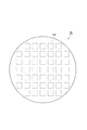
図1は、一実施形態に係る多層膜をエッチングする方法を示す流れ図である。図1に示す方法MTは、多層膜をエッチングするために、第1のプラズマ処理を実行する工程ST1、及び、多層膜を更にエッチングするために、第2のプラズマ処理を実行する工程ST2を含む。図2は、図1に示す方法が適用される被加工物を例示する平面図である。図3は、図2に示す被加工物の一つのパターン領域の一部分を拡大して示す平面図である。図4の(a)は、図3の部分Aの拡大平面図であり、図4の(b)は、図3の部分Aにおける被加工物の拡大断面図である。 FIG. 1 is a flow chart showing a method of etching a multilayer film according to an embodiment. The method MT shown in FIG. 1 includes a step ST1 of executing a first plasma treatment for etching the multilayer film and a step ST2 of executing a second plasma treatment for further etching the multilayer film. .. FIG. 2 is a plan view illustrating an workpiece to which the method shown in FIG. 1 is applied. FIG. 3 is an enlarged plan view showing a part of one pattern region of the work piece shown in FIG. FIG. 4A is an enlarged plan view of a portion A of FIG. 3, and FIG. 4B is an enlarged cross-sectional view of a work piece in a portion A of FIG.
図2に示すように、一例の被加工物Wは、ウエハのように略円盤形状を有し得る。図4の(b)に示すように、被加工物Wは、多層膜MF及びマスクIMを有する。多層膜MFは下地層UL上に設けられている。多層膜MFは、複数のシリコン酸化膜F1と複数のシリコン窒化膜F2を含んでいる。複数のシリコン酸化膜F1と複数のシリコン窒化膜F2は、交互に積層されている。多層膜MFにおけるシリコン酸化膜F1の個数、及び、シリコン窒化膜F2の個数の各々は、任意の個数であり得る。多層膜MFの全ての膜のうち最下層の膜は、シリコン酸化膜F1であってもよく、シリコン窒化膜F2であってもよい。また、多層膜MFの全ての膜のうち最上層の膜は、シリコン酸化膜F1であってもよく、シリコン窒化膜F2であってもよい。マスクIMは、多層膜MF上に設けられている。マスクIMは、炭素を含んでいる。マスクIMは、例えば、アモルファスカーボン製である。マスクIMには、複数の開口IMOが形成されている。複数の開口IMOの各々は、例えば円形の平面形状を有し得る。なお、マスクIMは、方法MTが被加工物Wに適用される前の状態の初期のマスクである。複数の開口IMOの各々は、当該初期のマスクにおける開口である。 As shown in FIG. 2, the workpiece W of one example may have a substantially disk shape like a wafer. As shown in FIG. 4B, the workpiece W has a multilayer film MF and a mask IM. The multilayer film MF is provided on the base layer UL. The multilayer film MF includes a plurality of silicon oxide films F1 and a plurality of silicon nitride films F2. The plurality of silicon oxide films F1 and the plurality of silicon nitride films F2 are alternately laminated. Each of the number of silicon oxide films F1 and the number of silicon nitride films F2 in the multilayer film MF can be arbitrary. The lowest layer of all the layers of the multilayer film MF may be a silicon oxide film F1 or a silicon nitride film F2. Further, the uppermost film of all the layers of the multilayer film MF may be a silicon oxide film F1 or a silicon nitride film F2. The mask IM is provided on the multilayer membrane MF. Mask IM contains carbon. The mask IM is made of, for example, amorphous carbon. A plurality of opening IMOs are formed in the mask IM. Each of the plurality of aperture IMOs can have, for example, a circular planar shape. The mask IM is an initial mask in a state before the method MT is applied to the workpiece W. Each of the plurality of aperture IMOs is an aperture in the initial mask.
図2に示すように、被加工物Wは、複数のパターン領域PRを有し得る。図2では、破線によって複数のパターン領域PRの各々の境界が示されている。複数のパターン領域PRは、互いに離れている。なお、複数のパターン領域PRの配置は図2に示されるものに限定されるものでない。図3に示すように、複数のパターン領域PRの各々には、複数の開口IMOが形成されている。図3に示すように、複数の開口IMOが形成されているマスクIMには、高い密度で開口IMOが形成されている領域DRと低い密度で開口IMOがされている領域IRが存在する。 As shown in FIG. 2, the workpiece W may have a plurality of pattern region PRs. In FIG. 2, the broken line indicates the boundary of each of the plurality of pattern area PRs. The plurality of pattern area PRs are separated from each other. The arrangement of the plurality of pattern area PRs is not limited to that shown in FIG. As shown in FIG. 3, a plurality of opening IMOs are formed in each of the plurality of pattern region PRs. As shown in FIG. 3, in the mask IM in which a plurality of opening IMOs are formed, there are a region DR in which the opening IMOs are formed at a high density and a region IR in which the opening IMOs are formed at a low density.
方法MTでは、上述の工程ST1及び工程ST2がプラズマ処理装置を用いて実行される。図5は、図1に示す方法の実行において用いることが可能なプラズマ処理装置を概略的に示す図である。図5に示すプラズマ処理装置10は、容量結合型プラズマエッチング装置である。プラズマ処理装置10は、チャンバ本体12を備えている。チャンバ本体12は、略円筒形状を有している。チャンバ本体12は、その内部空間をチャンバ12cとして提供している。チャンバ本体12は、例えばアルミニウムから形成されている。チャンバ本体12の内壁面には、耐プラズマ性を有する処理が施されている。例えば、チャンバ本体12の内壁面には、陽極酸化処理が施されている。チャンバ本体12は、電気的に接地されている。
In the method MT, the above-mentioned steps ST1 and ST2 are executed using the plasma processing apparatus. FIG. 5 is a diagram schematically showing a plasma processing apparatus that can be used in performing the method shown in FIG. The
また、チャンバ本体12の側壁には、通路12pが形成されている。被加工物Wは、チャンバ12cに搬入されるとき、また、チャンバ12cから搬出されるときに、通路12pを通る。この通路12pは、ゲートバルブ12gにより開閉可能となっている。
Further, a
チャンバ本体12の底部上には、支持部13が設けられている。支持部13は、絶縁材料から形成されている。支持部13は、略円筒形状を有している。支持部13は、チャンバ12c内において、チャンバ本体12の底部から鉛直方向に延在している。支持部13は、ステージ14を支持している。ステージ14は、チャンバ12c内に設けられている。
A
ステージ14は、下部電極18及び静電チャック20を有している。ステージ14は、電極プレート16を更に備え得る。電極プレート16は、例えばアルミニウムといった導体から形成されており、略円盤形状を有している。下部電極18は、電極プレート16上に設けられている。下部電極18は、例えばアルミニウムといった導体から形成されており、略円盤形状を有している。下部電極18は、電極プレート16に電気的に接続されている。
The
静電チャック20は、下部電極18上に設けられている。静電チャック20の上面の上には、被加工物Wが載置される。静電チャック20は、誘電体から形成された本体を有する。静電チャック20の本体内には、膜状の電極が設けられている。静電チャック20の電極は、スイッチを介して直流電源22に接続されている。静電チャック20の電極に直流電源22からの電圧が印加されると、静電チャック20と被加工物Wとの間で静電引力が発生する。発生した静電引力により、被加工物Wは静電チャック20に引き付けられ、当該静電チャック20によって保持される。
The
下部電極18の周縁部上には、被加工物Wのエッジを囲むように、フォーカスリングFRが配置される。フォーカスリングFRは、エッチングの均一性を向上させるために設けられている。フォーカスリングFRは、限定されるものではないが、シリコン、炭化シリコン、又は、石英から形成され得る。
A focus ring FR is arranged on the peripheral edge of the
下部電極18の内部には、流路18fが設けられている。流路18fには、チャンバ本体12の外部に設けられているチラーユニット26から配管26aを介して熱交換媒体(例えば冷媒)が供給される。流路18fに供給された熱交換媒体は、配管26bを介してチラーユニット26に戻される。プラズマ処理装置10では、静電チャック20上に載置された被加工物Wの温度が、熱交換媒体と下部電極18との熱交換により、調整される。
A
プラズマ処理装置10には、ガス供給ライン28が設けられている。ガス供給ライン28は、伝熱ガス供給機構からの伝熱ガス、例えばHeガスを、静電チャック20の上面と被加工物Wの裏面との間に供給する。
The
プラズマ処理装置10は、上部電極30を更に備えている。上部電極30は、ステージ14の上方に設けられている。上部電極30は、部材32を介して、チャンバ本体12の上部に支持されている。部材32は、絶縁性を有する材料から形成されている。上部電極30は、天板34及び支持体36を含み得る。天板34の下面は、チャンバ12c側の下面であり、チャンバ12cを画成している。天板34は、ジュール熱の少ない低抵抗の導電体又は半導体から形成され得る。天板34には、複数のガス吐出孔34aが形成されている。複数のガス吐出孔34aは、当該天板34をその板厚方向に貫通している。
The
支持体36は、天板34を着脱自在に支持するものであり、例えばアルミニウムといった導電性材料から形成され得る。支持体36の内部には、ガス拡散室36aが設けられている。ガス拡散室36aからは、複数のガス吐出孔34aにそれぞれ連通する複数のガス通流孔36bが下方に延びている。支持体36には、ガス拡散室36aに処理ガスを導くガス導入口36cが形成されている。ガス導入口36cには、ガス供給管38が接続されている。
The
ガス供給管38には、バルブ群42及び流量制御器群44を介して、ガスソース群40が接続されている。ガスソース群40は、複数のガスソースを含んでいる。複数のガスソースは、方法MTで利用される処理ガスを構成する複数のガスのソースを含んでいる。バルブ群42は、複数の開閉バルブを含んでいる。流量制御器群44は、複数の流量制御器を含んでいる。複数の流量制御器の各々は、マスフローコントローラ又は圧力制御式の流量制御器である。ガスソース群40の複数のガスソースは、バルブ群42の対応のバルブ、及び、流量制御器群44の対応の流量制御器を介してガス供給管38に接続されている。
A
プラズマ処理装置10では、チャンバ本体12の内壁に沿って、シールド46が着脱自在に設けられている。シールド46は、支持部13の外周にも設けられている。シールド46は、チャンバ本体12にエッチング副生物が付着することを防止する。シールド46は、例えば、アルミニウム材にY2O3等のセラミックスを被覆することにより構成され得る。
In the
支持部13とチャンバ本体12の側壁との間には、バッフルプレート48が設けられている。バッフルプレート48は、例えば、アルミニウム製の母材にY2O3等のセラミックスを被覆することにより構成される。バッフルプレート48には、複数の貫通孔が形成されている。バッフルプレート48の下方、且つ、チャンバ本体12の底部には、排気口12eが設けられている。排気口12eには、排気管52を介して排気装置50が接続されている。排気装置50は、圧力制御弁、及び、ターボ分子ポンプといった真空ポンプを有している。
A
プラズマ処理装置10は、第1の高周波電源62及び第2の高周波電源64を更に備えている。第1の高周波電源62は、プラズマ生成用の第1の高周波を発生する電源である。第1の高周波の周波数は、例えば、27MHz〜100MHzの範囲内の周波数である。第1の高周波電源62は、整合器66及び電極プレート16を介して下部電極18に接続されている。整合器66は、第1の高周波電源62の出力インピーダンスと負荷側(下部電極18側)の入力インピーダンスを整合させるための回路を有している。なお、第1の高周波電源62は、整合器66を介して、上部電極30に接続されていてもよい。
The
第2の高周波電源64は、被加工物Wにイオンを引き込むための第2の高周波を発生する電源である。第2の高周波の周波数は、第1の高周波の周波数よりも低い。第2の高周波の周波数は、例えば400kHz〜13.56MHzの範囲内の周波数である。第2の高周波電源64は、整合器68及び電極プレート16を介して下部電極18に接続されている。整合器68は、第2の高周波電源64の出力インピーダンスと負荷側(下部電極18側)の入力インピーダンスを整合させるための回路を有している。
The second high
プラズマ処理装置10は、直流電源部70を更に備え得る。直流電源部70は、上部電極30に接続されている。直流電源部70は、負の直流電圧を発生し、当該直流電圧を上部電極30に与えることが可能である。
The
プラズマ処理装置10は、制御部Cntを更に備え得る。制御部Cntは、プロセッサ、記憶部、入力装置、表示装置等を備えるコンピュータであり得る。制御部Cntは、プラズマ処理装置10の各部を制御する。制御部Cntでは、入力装置を用いて、オペレータがプラズマ処理装置10を管理するためにコマンドの入力操作等を行うことができる。また、制御部Cntでは、表示装置により、プラズマ処理装置10の稼働状況を可視化して表示することができる。さらに、制御部Cntの記憶部には、プラズマ処理装置10で実行される各種処理をプロセッサにより制御するための制御プログラム、及び、レシピデータが格納されている。制御部Cntのプロセッサが制御プログラムを実行して、レシピデータに従ってプラズマ処理装置10の各部を制御することにより、方法MTがプラズマ処理装置10で実行される。
The
再び図1を参照する。以下、プラズマ処理装置10を用いて図2、図3、図4の(a)、及び、図4の(b)に示した被加工物Wに適用される場合を例にとって、方法MTを説明する。なお、方法MTが適用される対象は、被加工物Wに限定されるものではない。また、方法MTは、プラズマ処理装置10以外のプラズマ処理装置を用いて実行されてもよい。
See FIG. 1 again. Hereinafter, the method MT will be described by taking as an example the case where the
方法MTは、被加工物Wがプラズマ処理装置10のチャンバ12c内で静電チャック20上に載置された状態で実行される。方法MTでは、まず、工程ST1において、第1のプラズマ処理が実行される。方法MTでは、続く工程ST2において、第2のプラズマ処理が実行される。
The method MT is performed with the workpiece W mounted on the
工程ST1の第1のプラズマ処理及び工程ST2の第2のプラズマ処理において、チャンバ内では処理ガスのプラズマが生成される。処理ガスは、水素原子、フッ素原子、及び、炭素原子を含み、且つ、硫黄含有ガスを含む。処理ガスは、水素原子を含めるために、H2ガス、CxHyガス(炭化水素ガス)、及び、CxHyFzガス(ハイドロフルオロカーボンガス)のうち一種以上のガスを含む。処理ガスは、フッ素原子を含めるために、フッ素含有ガスを含んでいる。フッ素含有ガスは、HFガス、NF3ガス、SF6ガス、WF6ガス、CxFYガス(フルオロカーボンガス)、及び、CxHyFzガス、のうち一種以上のガスを含む。処理ガスは、炭素原子を含めるために、CxHyガス(炭化水素ガス)、及び、CxHyFzガス(ハイドロフルオロカーボンガス)のうち一種以上のガスを含む。なお、x、y、zは、自然数である。また、処理ガスは、硫黄含有ガスとして、H2Sガス、COSガス、CH3SHガス、SBr2ガス、S2Br2ガス、SF2ガス、S2F2ガス、SF4ガス、SF6ガス、S2F10ガス、SCl2ガス、S2Cl2ガス、及び、S3Cl3ガスのうち一種以上のガスを含み得る。なお、処理ガスは、HBrガスといったハロゲン含有ガスを更に含んでいてもよい。また、処理ガスは、O2ガス、COガス、CO2ガスといった酸素含有ガスを含んでいてもよい。一例においては、処理ガスは、水素ガス、ハイドフルオロカーボンガス、及び、フッ素含有ガスを含む混合ガスである。より具体的な一例では、処理ガスは、H2ガス、CH2F2ガス、SF6ガス、及び、HBrガスを含む混合ガスであり得る。 In the first plasma treatment of step ST1 and the second plasma treatment of step ST2, plasma of the processing gas is generated in the chamber. The processing gas contains a hydrogen atom, a fluorine atom, and a carbon atom, and also contains a sulfur-containing gas. The processing gas includes one or more of H 2 gas, CxHy gas (hydrocarbon gas), and CxHyFz gas (hydrofluorocarbon gas) in order to contain hydrogen atoms. The processing gas contains a fluorine-containing gas in order to contain fluorine atoms. The fluorine-containing gas includes one or more of HF gas, NF 3 gas, SF 6 gas, WF 6 gas, CxF Y gas (fluorocarbon gas), and CxHyFz gas. The treatment gas includes one or more of CxHy gas (hydrocarbon gas) and CxHyFz gas (hydrofluorocarbon gas) in order to contain carbon atoms. Note that x, y, and z are natural numbers. The processing gas is H 2 S gas, COS gas, CH 3 SH gas, SBr 2 gas, S 2 Br 2 gas, SF 2 gas, S 2 F 2 gas, SF 4 gas, SF 6 as sulfur-containing gas. It may contain one or more of the gases, S 2 F 10 gas, S Cl 2 gas, S 2 Cl 2 gas, and S 3 Cl 3 gas. The processing gas may further contain a halogen-containing gas such as HBr gas. Further, the processing gas may contain an oxygen-containing gas such as O 2 gas, CO gas and CO 2 gas. In one example, the processing gas is a mixed gas containing hydrogen gas, hydrate fluorocarbon gas, and fluorine-containing gas. In a more specific example, the processing gas can be a mixed gas containing H 2 gas, CH 2 F 2 gas, SF 6 gas, and HBr gas.
工程ST1の第1のプラズマ処理及び工程ST2の第2のプラズマ処理において、被加工物Wの温度は、−15℃以下の温度に設定される。被加工物Wの温度は、流路18fに供給される熱交換媒体の温度により調整される。
In the first plasma treatment of step ST1 and the second plasma treatment of step ST2, the temperature of the workpiece W is set to a temperature of −15 ° C. or lower. The temperature of the workpiece W is adjusted by the temperature of the heat exchange medium supplied to the
工程ST1では、チャンバ12cの圧力が第1の圧力に設定され、工程ST2では、チャンバ12cの圧力が第2の圧力に設定される。第1の圧力は、第2の圧力よりも低い。例えば、第1の圧力は、2Pa(パスカル)、即ち15mTorr以下であり、第2の圧力は3.333Pa(パスカル)、即ち25mTorr以上である。
In step ST1, the pressure in the
一実施形態では、方法MTの実行後に多層膜MFに形成されるべき開口OPの所望のアスペクト比の半分以上、且つ、当該所望のアスペクト比よりも小さいアスペクト比を有する開口が多層膜MFに形成されるまで、工程ST1が実行される。しかる後に、所望のアスペクト比の開口OPが形成されるまで、工程ST2が実行される。 In one embodiment, an opening having at least half the desired aspect ratio of the opening OP to be formed in the multilayer MF after execution of the method MT and an aspect ratio smaller than the desired aspect ratio is formed in the multilayer MF. Step ST1 is executed until this is done. After that, step ST2 is executed until an opening OP having a desired aspect ratio is formed.
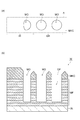
以下、図6の(a)、図6の(b)、図7の(a)、及び、図7の(b)を参照する。図6の(a)は、硫黄含有ガスを含まない処理ガスを用いたプラズマエッチング中のマスクの一部領域の平面図であり、図6の(b)は、硫黄含有ガスを含まない処理ガスを用いたプラズマエッチング中の被加工物の断面図である。図7の(a)は、硫黄含有ガスを含む処理ガスを用いたプラズマエッチング中のマスクの一部領域の平面図であり、図7の(b)は、硫黄含有ガスを含む処理ガスを用いたプラズマエッチング中の被加工物の断面図である。 Hereinafter, reference is made to FIG. 6A, FIG. 6B, FIG. 7A, and FIG. 7B. FIG. 6A is a plan view of a part of the mask during plasma etching using a processing gas containing no sulfur-containing gas, and FIG. 6B is a processing gas containing no sulfur-containing gas. It is sectional drawing of the workpiece during plasma etching using. FIG. 7A is a plan view of a part of the mask during plasma etching using a processing gas containing a sulfur-containing gas, and FIG. 7B is a processing gas containing a sulfur-containing gas. It is sectional drawing of the workpiece during plasma etching.
硫黄含有ガスを含まず、炭素原子、フッ素原子、及び、水素原子を含む処理ガスのプラズマを用いた多層膜MFのエッチングでは、マスク上に炭素を含有する堆積物が形成される。プラズマエッチング中には、堆積物、又は、堆積物及びマスクが、それらと反応する活性種によってエッチングされることにより、マスクMKCの複数の開口MOの形状が定められる。即ち、初期のマスクIMの残部、又は、初期のマスクIMの残部と堆積物によって、プラズマエッチング中のマスクMKCの複数の開口MOの形状が定められる。なお、活性種は、多層膜MFのエッチング中に発生する酸素を含む。 Etching of the multilayer film MF using plasma of a processing gas containing carbon atoms, fluorine atoms, and hydrogen atoms, which does not contain a sulfur-containing gas, forms carbon-containing deposits on the mask. During plasma etching, the deposits, or the deposits and the mask, are etched by the active species that react with them, thereby defining the shape of the plurality of openings MO of the mask MKC. That is, the shape of the plurality of openings MO of the mask MKC during plasma etching is determined by the remnants of the initial mask IM or the remnants and deposits of the initial mask IM. The active species contains oxygen generated during etching of the multilayer film MF.
多層膜MFのエッチング中に発生する酸素の量は、高い密度で開口MOが形成されている領域DRでは多く、低い密度で開口MOが形成されている領域IRでは少ない。したがって、図6の(a)及び図6の(b)に示すように、マスクMKCの幾つかの開口MOが変形する。例えば、領域IRの幾つかの開口MOの平面形状が円形から変形する。その結果、マスクMKCの複数の開口MOの形状が不均一になる。マスクMKCの複数の開口MOの形状が不均一になると、これら複数の開口MOの下方において多層膜MFが均一にエッチングされず、多層膜MFに形成される複数の開口OPの形状が、不均一になり、当該複数の開口OPの垂直性が低くなる。 The amount of oxygen generated during etching of the multilayer film MF is large in the region DR in which the aperture MO is formed at a high density, and is small in the region IR in which the aperture MO is formed at a low density. Therefore, as shown in (a) of FIG. 6 and (b) of FIG. 6, some opening MOs of the mask MKC are deformed. For example, the planar shape of some openings MO in the region IR is deformed from circular. As a result, the shapes of the plurality of openings MO of the mask MKC become non-uniform. When the shapes of the plurality of openings MO of the mask MKC become non-uniform, the multilayer film MF is not uniformly etched below the plurality of openings MO, and the shapes of the plurality of openings OP formed on the multilayer film MF become non-uniform. Therefore, the verticality of the plurality of openings OP becomes low.
一方、方法MTでは、硫黄含有ガス中の硫黄を含む堆積物がマスク上に形成され、当該マスクと堆積物によって、プラズマエッチング中のマスクMKの複数の開口MOの形状が定められる。硫黄を含む堆積物の膜は、比較的均一な膜厚でマスク上に形成される。したがって、方法MTによれば、図7の(a)及び図7の(b)に示すように、プラズマエッチング中にマスクMKの複数の開口MOの変形が抑制され、マスクMKの複数の開口MOの形状の均一性が高められる。 On the other hand, in the method MT, a deposit containing sulfur in the sulfur-containing gas is formed on the mask, and the shape of the plurality of openings MO of the mask MK during plasma etching is determined by the mask and the deposit. A film of sulfur-containing deposits is formed on the mask with a relatively uniform film thickness. Therefore, according to the method MT, as shown in (a) of FIG. 7 and (b) of FIG. 7, deformation of the plurality of openings MO of the mask MK is suppressed during plasma etching, and the plurality of openings MO of the mask MK are suppressed. The uniformity of the shape of is improved.
しかしながら、硫黄含有ガスが処理ガスに含められると、マスクが比較的大きくエッチングされる。即ち、選択性が低くなる。方法MTでは、選択性を高めるために、静電チャック20の温度が−15℃以下の温度に設定される。静電チャック20の温度が−15℃以下の温度に設定されると、多層膜MFのエッチングレートが高くなる。したがって、選択性が高くなる。
However, when the sulfur-containing gas is included in the processing gas, the mask is etched relatively large. That is, the selectivity becomes low. In the method MT, the temperature of the
但し、静電チャック20の温度が−15℃以下の温度に設定されると、多層膜MFの積層方向に対して多層膜MFに形成される開口に曲がりが生じる。多層膜MFに形成される開口の曲がりを抑制するために、方法MTでは、工程ST1におけるチャンバ12cの第1の圧力が、工程ST2におけるチャンバ12cの第2の圧力よりも低い圧力に設定される。チャンバ12cの圧力が低い場合には、積層方向に延びる垂直性の高い開口OPが多層膜MFに形成されるが、選択性が低くなる。一方、チャンバ12cの圧力が高い場合には、多層膜MFのエッチングにおいて選択性を高めることができる。したがって、方法MTによれば、選択性を高め、且つ、多層膜MFに形成される複数の開口OPの形状の均一性及び垂直性を高めることができる。
However, when the temperature of the
以上、方法MTの実施形態について説明してきたが、上述した実施形態に限定されることなく種々の変形態様を構成可能である。方法MTには、容量結合型のプラズマ処理装置以外のプラズマ処理装置を用いることができる。例えば、方法MTには、誘導結合型のプラズマ処理装置、又は、マイクロ波といった表面波を用いてプラズマを生成するプラズマ処理装置を用いることができる。 Although the embodiment of the method MT has been described above, various modifications can be configured without being limited to the above-described embodiment. As the method MT, a plasma processing device other than the capacitive coupling type plasma processing device can be used. For example, as the method MT, an inductively coupled plasma processing apparatus or a plasma processing apparatus that generates plasma using a surface wave such as a microwave can be used.
以下、方法MTの評価のために行った種々の実験について説明する。まず、実験において求めた幾つか評価値について、それらの定義を説明する。なお、以下に説明する評価値の取得のために行った実験では、初期のマスク、即ちプラズマエッチング前のマスクの開口の平面形状は円形であった。 Hereinafter, various experiments performed for the evaluation of the method MT will be described. First, the definitions of some evaluation values obtained in the experiment will be described. In the experiment conducted for obtaining the evaluation values described below, the planar shape of the opening of the initial mask, that is, the mask before plasma etching was circular.
幾つかの実験では、評価値として、面積比を求めた。「面積比」は、実験のプラズマエッチング後のマスクのパターン領域PRの中心部の開口MOの面積によって、当該プラズマエッチング後のマスクのパターン領域PRの端部の開口MOの面積を除した値である。「面積比」は、その値が1に近いほど、マスクの複数の開口MOの形状が均一であることを表す。 In some experiments, the area ratio was determined as an evaluation value. The "area ratio" is a value obtained by dividing the area of the opening MO at the end of the pattern region PR of the mask after plasma etching by the area of the opening MO at the center of the pattern region PR of the mask after plasma etching in the experiment. be. The "area ratio" means that the closer the value is to 1, the more uniform the shape of the plurality of openings MO of the mask.
また、幾つかの実験では、扁平率を求めた。「扁平率」は、実験のプラズマエッチング後のマスクのパターン領域PRの端部の開口MOの長径と短径の差を、当該長径により除した値である。「扁平率」は、その値が0に近いほど、パターン領域PRの端部、即ち、粗領域でのマスクの開口の変形(歪み)が少ないことを表す。 Also, in some experiments, the flattening was determined. The "flatness" is a value obtained by dividing the difference between the major axis and the minor axis of the opening MO at the end of the pattern region PR of the mask after plasma etching in the experiment by the major axis. The "flatness" means that the closer the value is to 0, the less the deformation (distortion) of the mask opening at the end of the pattern region PR, that is, in the coarse region.
また、幾つかの実験では、変化率を求めた。変化率は、以下の式(1)で定義される。
変化率(%)=(P−Q)/P×100 …(1)
式(1)において、Pは、初期のマスクにおける二つの近傍の開口IMOの重心間の距離である。Qは、これら二つの近傍の開口IMOの下方でプラズマエッチングにより多層膜MFに形成された二つの開口OPの底部における重心間の距離である。変化率の平均値、及び、3×(変化率の標準偏差)、即ち変化率の3σが小さければ、多層膜MFに形成された複数の開口OPの形状が均一であり、且つ、当該複数の開口OPの垂直性が高い。
In some experiments, the rate of change was determined. The rate of change is defined by the following equation (1).
Rate of change (%) = (PQ) / P × 100… (1)
In equation (1), P is the distance between the centers of gravity of the two nearby aperture IMOs in the initial mask. Q is the distance between the centers of gravity at the bottoms of the two opening OPs formed in the multilayer film MF by plasma etching below these two nearby openings IMO. If the average value of the rate of change and 3 × (standard deviation of the rate of change), that is, the rate of change of 3σ is small, the shapes of the plurality of openings OP formed in the multilayer membrane MF are uniform, and the plurality of openings OP are uniform. The verticality of the opening OP is high.
また、幾つかの実験では、選択比を求めた。選択比は、多層膜のエッチングレートをマスクのエッチングレートで除した値として定義される。選択比は、その値が大きいほど、マスクのエッチングを抑制しつつ、多層膜をエッチングすることができること、即ち、選択性が高いことを示す。 Also, in some experiments, the selectivity was determined. The selectivity is defined as the etching rate of the multilayer film divided by the etching rate of the mask. The larger the selectivity ratio, the higher the selectivity, that is, the more the multilayer film can be etched while suppressing the etching of the mask.
(第1の実験) (First experiment)
第1の実験では、図2、図3、図4(a)、及び、図4の(b)に示した被加工物Wを準備し、プラズマ処理装置10を用いて多層膜MFのプラズマエッチングを行い、多層膜MFに形成された複数の開口OPのアスペクト比と、面積比、扁平率、及び、マスクのエッチングレートの各々との関係を求めた。第1の実験では、処理ガスが3.5%の流量比でH2Sガスを含む条件と処理ガスがH2Sガスを含まない条件のそれぞれで、多層膜MFのプラズマエッチングを行った。なお、H2Sガスの流量比は、処理ガスの全流量に対するH2Sガスの流量の比である。第1の実験におけるプラズマエッチングのその他の条件を以下に示す。
In the first experiment, the workpiece W shown in FIGS. 2, 3, 4 (a), and 4 (b) was prepared, and plasma etching of the multilayer film MF was performed using the
<第1の実験におけるプラズマエッチングの条件>
・処理ガス:H2ガス、CH2F2ガス、H2Sガス、及び、HBrガスを含む混合ガス
・チャンバ12cの圧力:3.333Pa(25mTorr)
・静電チャック20の温度:0℃
・第1の高周波:2.5kW、40MHz、連続波
・第2の高周波:7kW、0.4MHz、連続波
<Plasma etching conditions in the first experiment>
-Treatment gas: Pressure of
-Temperature of electrostatic chuck 20: 0 ° C
・ First high frequency: 2.5kW, 40MHz, continuous wave ・ Second high frequency: 7kW, 0.4MHz, continuous wave
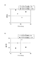
図8の(a)は、第1の実験において求めたアスペクト比と面積比との関係を示すグラフであり、図8の(b)に、第1の実験において求めたアスペクト比と扁平率との関係を示すグラフである。図9は、第1の実験において求めたアスペクト比とマスクのエッチングレートとの関係を示すグラフである。図8の(a)及び図8の(b)に示すように、H2Sガスを含む処理ガスを用いたプラズマエッチングでは、H2Sガスを含まない処理ガスを用いたプラズマエッチングに比べて、面積比が1に近く、偏平率が小さかった。即ち、硫黄含有ガスの一種であるH2Sガスを処理ガスに含めることで、パターン領域PRの端部におけるマスクの開口の変形が抑制され、且つ、マスクの複数の開口の形状が均一になることが確認された。但し、図9に示すように、H2Sガスを含む処理ガスを用いたプラズマエッチングでは、H2Sガスを含まない処理ガスを用いたプラズマエッチングに比べて、マスクのエッチングレートが高かった。即ち、H2Sガスを含む処理ガスを用いたプラズマエッチングでは、H2Sガスを含まない処理ガスを用いたプラズマエッチングに比べて、選択性が低くなっていた。 FIG. 8A is a graph showing the relationship between the aspect ratio and the area ratio obtained in the first experiment, and FIG. 8B shows the aspect ratio and the flatness obtained in the first experiment. It is a graph which shows the relationship of. FIG. 9 is a graph showing the relationship between the aspect ratio obtained in the first experiment and the etching rate of the mask. As shown in (a) in and FIG. 8 (b) of FIG. 8, in the plasma etching using a processing gas containing H 2 S gas, in comparison with the plasma etching using the process gas containing no H 2 S gas The area ratio was close to 1, and the flatness was small. That is, by including the H 2 S gas is a kind of sulfur-containing gas to the processing gas, the deformation of the mask openings of the ends of the pattern region PR been suppressed and, becomes uniform shape of the plurality of openings of the mask It was confirmed that. However, as shown in FIG. 9, in the plasma etching using a processing gas containing H 2 S gas, in comparison with the plasma etching using the process gas containing no H 2 S gas, the etching rate of the mask was high. That is, in the plasma etching using a processing gas containing H 2 S gas, in comparison with the plasma etching using the process gas containing no H 2 S gas, it had lower selectivity.
(第2の実験) (Second experiment)
第2の実験では、第1の実験で用いた被加工物と同様の被加工物Wを準備し、プラズマ処理装置10を用いて多層膜MFのプラズマエッチングを行い、静電チャック20の温度と、選択比及び変化率の3σの各々との関係を求めた。以下に、第2の実験におけるプラズマエッチングの条件を示す。なお、第2の条件においては、処理ガスは、SF6ガスを3.5%の流量比で含んでいた。
In the second experiment, a workpiece W similar to the workpiece used in the first experiment was prepared, plasma etching of the multilayer film MF was performed using the
<第2の実験におけるプラズマエッチングの条件>
・処理ガス:H2ガス、CH2F2ガス、SF6ガス、及び、HBrガスを含む混合ガス
・チャンバ12cの圧力:3.333Pa(25mTorr)
・第1の高周波:2.5kW、40MHz、連続波
・第2の高周波:7kW、0.4MHz、連続波
・多層膜MFに形成した開口OPのアスペクト比:80
<Plasma etching conditions in the second experiment>
-Processing gas:
・ First high frequency: 2.5 kW, 40 MHz, continuous wave ・ Second high frequency: 7 kW, 0.4 MHz, continuous wave ・ Aspect ratio of opening OP formed in multilayer film MF: 80
図10の(a)は、第2の実験において求めた静電チャックの温度と選択比との関係を示すグラフであり、図10の(b)は、第2の実験において求めた静電チャックの温度と変化率の3σとの関係を示すグラフである。図10の(a)に示すように、静電チャックの温度が低下すると、選択比が高くなっていた。したがって、静電チャックの温度を低い温度に設定することにより、選択性を改善できることが確認された。一方、図10の(b)に示すように、静電チャックの温度が低下すると、変化率の3σが大きくなっていた。したがって、静電チャックの温度が低下すると、多層膜MFに形成された複数の開口OPの形状が不均一になることが確認された。 FIG. 10 (a) is a graph showing the relationship between the temperature of the electrostatic chuck obtained in the second experiment and the selection ratio, and FIG. 10 (b) is the electrostatic chuck obtained in the second experiment. It is a graph which shows the relationship between the temperature of 3σ and the rate of change of 3σ. As shown in FIG. 10A, the selectivity increased as the temperature of the electrostatic chuck decreased. Therefore, it was confirmed that the selectivity can be improved by setting the temperature of the electrostatic chuck to a low temperature. On the other hand, as shown in FIG. 10B, when the temperature of the electrostatic chuck decreased, the rate of change of 3σ increased. Therefore, it was confirmed that when the temperature of the electrostatic chuck decreases, the shapes of the plurality of openings OP formed on the multilayer film MF become non-uniform.
(第3の実験) (Third experiment)
第3の実験では、プラズマ処理装置10を用いて第2の実験と同様の条件で、シリコン酸化膜及びシリコン窒化膜のエッチングを行った。第3の実験では、静電チャック20の温度とエッチングレートの平均値との関係を求めた。エッチングレートの平均値は、シリコン酸化膜のエッチングレートとシリコン窒化膜のエッチングレートとの平均値である。図11は、第3の実験において求めた静電チャックの温度とエッチングレートの平均値との関係を示すグラフである。図11に示すように、静電チャックの温度が−15℃以下である場合に、相当に高いエッチングレートの平均値が得られていた。したがって、静電チャックの温度を−15℃以下に設定することで、多層膜MFのエッチングレートを高め、選択性を高めることが可能であることが確認された。
In the third experiment, the silicon oxide film and the silicon nitride film were etched using the
(第4の実験) (Fourth experiment)
第4の実験では、処理ガスに含める硫黄含有ガスとしてSF6ガスを用いた。第4の実験では、第1の実験で用いた被加工物と同様の被加工物Wを準備し、プラズマ処理装置10を用いて多層膜MFのプラズマエッチングを行い、SF6ガスの流量比と、面積比、マスクのパターン領域PRの中心部の開口MOの扁平率、マスクのパターン領域PRの端部の開口MOの扁平率、変化率の平均値、及び、変化率の3σの各々との関係を求めた。なお、SF6ガスの流量比は、処理ガスの全流量に対するSF6ガスの流量の比である。以下に、第4の実験におけるプラズマエッチングの条件を示す。
In the fourth experiment, SF 6 gas was used as the sulfur-containing gas to be included in the processing gas. In the fourth experiment, a workpiece W similar to the workpiece used in the first experiment was prepared, plasma etching of the multilayer film MF was performed using the
<第4の実験におけるプラズマエッチングの条件>
・処理ガス:H2ガス、CH2F2ガス、HBrガス、及び、SF6ガスを含む混合ガス
・チャンバ12cの圧力:3.333Pa(25mTorr)
・静電チャック20の温度:−40℃
・第1の高周波:2.5kW、40MHz、連続波
・第2の高周波:7kW、0.4MHz、連続波
・多層膜MFに形成した開口OPのアスペクト比:90
<Plasma etching conditions in the 4th experiment>
-Treatment gas: Pressure of
-Temperature of electrostatic chuck 20: -40 ° C
・ First high frequency: 2.5 kW, 40 MHz, continuous wave ・ Second high frequency: 7 kW, 0.4 MHz, continuous wave ・ Aspect ratio of opening OP formed in multilayer film MF: 90
図12の(a)は、第4の実験において求めたSF6ガスの流量比と面積比との関係を示すグラフであり、図12の(b)は、第4の実験において求めた、SF6ガスの流量比と、マスクのパターン領域の中心部の開口の扁平率及びマスクのパターン領域の端部の開口の扁平率の各々との関係を示すグラフである。硫黄含有ガスとしてH2Sガスに代えてSF6ガスを用いても、図12の(a)及び図12の(b)に示すように、面積比が1に近く、扁平率が小さかった。したがって、任意の硫黄含有ガスを用いることで、マスクの開口の変形が抑制され、且つ、マスクの複数の開口の形状が均一になるものと推測される。なお、SF6ガスの流量比が10%以上である場合に、マスクの開口の変形が更に抑制され、且つ、マスクの複数の開口の形状が更に均一になっていた。 FIG. 12A is a graph showing the relationship between the flow rate ratio and the area ratio of SF 6 gas obtained in the fourth experiment, and FIG. 12B is the SF obtained in the fourth experiment. 6 is a graph showing the relationship between the flow rate ratio of 6 gases, the flatness of the opening at the center of the pattern region of the mask, and the flatness of the opening at the end of the pattern region of the mask. Be used SF 6 gas in place of the H 2 S gas as a sulfur-containing gas, as shown in (a) in and FIG. 12 (b) of FIG. 12, the area ratio is close to 1, it was small aspect ratio. Therefore, it is presumed that by using an arbitrary sulfur-containing gas, the deformation of the openings of the mask is suppressed and the shapes of the plurality of openings of the mask become uniform. When the flow rate ratio of SF 6 gas was 10% or more, the deformation of the openings of the mask was further suppressed, and the shapes of the plurality of openings of the mask were more uniform.
図13は、第4の実験において求めた、SF6ガスの流量比と、変化率の平均値及び変化率の3σの各々との関係を示すグラフである。図13に示すように、変化率の平均値はSF6ガスの流量比に依存せず、略ゼロであった。また、SF6ガスの流量比に依存せず、変化率の3σは大きかった。したがって、第4の実験のプラズマエッチングの条件では、SF6ガスの流量比に依存せず、多層膜MFに形成された複数の開口OPの形状が不均一であることが確認された。なお、変化率の3σが大きいにもかかわらず変化率の平均値が小さくなっていたのは、多層膜MFの積層方向に対して開口OPが延在する方向にバラツキが生じており、正の値を有する変化率と負の値を有する変化率が存在していたことが原因であった。多層膜MFに形成される複数の開口OPの形状が不均一であり、且つ、複数の開口OPの垂直性が低ければ変化率の3σは大きくなるので、多層膜MFに形成される複数の開口OPの形状の均一性及び複数の開口OPの垂直性の双方は、変化率の3σのみを評価可能であることが第4の実験の結果から理解できる。 FIG. 13 is a graph showing the relationship between the flow rate ratio of SF 6 gas, the average value of the rate of change, and 3σ of the rate of change, which were obtained in the fourth experiment. As shown in FIG. 13, the average value of the rate of change did not depend on the flow rate ratio of SF 6 gas and was substantially zero. Moreover, the rate of change of 3σ was large regardless of the flow rate ratio of SF 6 gas. Therefore, under the plasma etching conditions of the fourth experiment, it was confirmed that the shapes of the plurality of opening OPs formed in the multilayer film MF were non-uniform, regardless of the flow rate ratio of the SF 6 gas. The reason why the average value of the rate of change was small despite the large rate of change of 3σ was that there was a variation in the direction in which the opening OP extended with respect to the stacking direction of the multilayer film MF, which was positive. The cause was that there was a rate of change with a value and a rate of change with a negative value. If the shapes of the plurality of openings OPs formed in the multilayer membrane MF are non-uniform and the verticality of the plurality of openings OPs is low, the rate of change of 3σ becomes large. Therefore, the plurality of openings formed in the multilayer membrane MFs. It can be understood from the result of the fourth experiment that both the uniformity of the shape of the OP and the verticality of the plurality of opening OPs can be evaluated only by the rate of change of 3σ.
(第5の実験) (Fifth experiment)
第5の実験では、第1の実験で用いた被加工物と同様の被加工物Wを準備し、プラズマ処理装置10を用いて多層膜MFのプラズマエッチングを行い、多層膜MFに形成された開口OPのアスペクト比と変化率の3σとの関係を求めた。以下に、第5の実験におけるプラズマエッチングの条件を示す。なお、第5の実験では、SF6ガスの流量比は14%であった。また、以下に示す通り、第5の実験では、チャンバ12cの圧力を、以下の条件5A,5B,5C,5Dのそれぞれに設定した。
In the fifth experiment, a workpiece W similar to the workpiece used in the first experiment was prepared, plasma etching of the multilayer film MF was performed using the
<第5の実験におけるプラズマエッチングの条件>
・処理ガス:H2ガス、CH2F2ガス、SF6ガス、及び、HBrガスを含む混合ガス
・チャンバ12cの圧力
条件5A:15mTorr(2Pa)で一定
条件5B:25mTorr(3.333Pa)で一定
条件5C
アスペクト比が40になるまで:15mTorr(2Pa)
アスペクト比が40になってから:25mTorr(3.333Pa)
条件5D:
アスペクト比が60になるまで:15mTorr(2Pa)
アスペクト比が60になってから:25mTorr(3.333Pa)
・静電チャック20の温度:−40℃
・第1の高周波:2.5kW、40MHz、連続波
・第2の高周波:7kW、0.4MHz、連続波
<Plasma etching conditions in the fifth experiment>
-Treatment gas: Pressure of
Until the aspect ratio reaches 40: 15mTorr (2Pa)
After the aspect ratio reaches 40: 25mTorr (3.333Pa)
Condition 5D:
Until the aspect ratio reaches 60: 15mTorr (2Pa)
After the aspect ratio reaches 60: 25mTorr (3.333Pa)
-Temperature of electrostatic chuck 20: -40 ° C
・ First high frequency: 2.5kW, 40MHz, continuous wave ・ Second high frequency: 7kW, 0.4MHz, continuous wave
図14は、第5の実験において求めたアスペクト比と変化率の3σとの関係を示すグラフである。図14に示すように、条件5Aのプラズマエッチング、即ち、チャンバ12cの圧力を15mTorr(2Pa)で変更しなかったプラズマエッチングでは、変化率の3σは小さかったが、選択性が低く、マスクMKを維持することができず高いアスペクト比の複数の開口を多層膜MFに形成することができなかった。条件5Bのプラズマエッチング、即ち、チャンバ12cの圧力を25mTorr(3.333Pa)で変更しなかったプラズマエッチングでは、多層膜MFに形成された複数の開口OPのアスペクト比が50よりも大きい場合には、変化率の3σが相当に大きくなった。
FIG. 14 is a graph showing the relationship between the aspect ratio obtained in the fifth experiment and the rate of change of 3σ. As shown in FIG. 14, in the plasma etching under the condition 5A, that is, in the plasma etching in which the pressure of the
一方、条件5C及び条件5Dの各々のプラズマエッチング、即ち、最初にチャンバ12cの圧力を比較的低い圧力に設定して第1のプラズマ処理を行い、次いでチャンバ12cの圧力を比較的高い圧力に設定して第2のプラズマ処理を行うプラズマエッチングでは、条件5Aのプラズマエッチングよりも高いアスペクト比の開口を多層膜MFに形成することができた。また、条件5C及び条件5Dの各々のプラズマエッチングでは、条件5Bのプラズマエッチングよりも小さい変化率の3σを有する複数の開口OPを多層膜MFに形成することができた。また、条件5Cの場合のプラズマエッチングに比べて、条件5Dのプラズマエッチングでは、より高いアスペクト比を有する複数の開口を相当に小さい変化率の3σで形成可能であることから、多層膜MFに形成されるべき開口OPの所望のアスペクト比の半分以上、且つ、所望のアスペクト比よりも小さいアスペクト比を有する開口が多層膜MFに形成されるまで、低圧でのプラズマ処理(第1のプラズマ処理)を実行し、次いで、高圧でのプラズマ処理(第2のプラズマ処理)を行うことで、選択性を高め、且つ、多層膜MFに形成される複数の開口OPの形状の均一性及び垂直性を更に高めることが可能であるものと考えられる。
On the other hand, plasma etching of each of the conditions 5C and 5D, that is, first the pressure of the
10…プラズマ処理装置、12…チャンバ本体、12c…チャンバ、14…ステージ、18…下部電極、20…静電チャック、50…排気装置、62…第1の高周波電源、64…第2の高周波電源、W…被加工物、MF…多層膜、F1…シリコン酸化膜、F2…シリコン窒化膜、IM,MK…マスク、PR…パターン領域、IMO,MO…開口、OP…開口。 10 ... Plasma processing device, 12 ... Chamber body, 12c ... Chamber, 14 ... Stage, 18 ... Lower electrode, 20 ... Electrostatic chuck, 50 ... Exhaust device, 62 ... First high frequency power supply, 64 ... Second high frequency power supply , W ... Work piece, MF ... Multilayer film, F1 ... Silicon oxide film, F2 ... Silicon nitride film, IM, MK ... Mask, PR ... Pattern area, IMO, MO ... Opening, OP ... Opening.
Claims (5)
前記多層膜は、交互に積層された複数のシリコン酸化膜及び複数のシリコン窒化膜を含み、
前記被加工物は、前記多層膜上に設けられた、炭素を含有するマスクを有し、
前記マスクには複数の開口が形成されており、
該方法は、前記被加工物がプラズマ処理装置のチャンバ内で静電チャック上に載置された状態で実行され、
前記多層膜をエッチングするために、第1のプラズマ処理を実行する工程と、
第1のプラズマ処理を実行する前記工程の後に前記多層膜を更にエッチングするために、第2のプラズマ処理を実行する工程と、
を含み、
第1のプラズマ処理を実行する前記工程及び第2のプラズマ処理を実行する前記工程において、前記多層膜をエッチングするために、前記静電チャックの温度が−15℃以下の温度に設定された状態で、前記チャンバ内で、処理ガスのプラズマが生成され、
前記処理ガスは、水素原子、フッ素原子、及び、炭素原子を含み、且つ、硫黄含有ガスを含み、
前記第2のプラズマ処理において前記多層膜のエッチングの前記マスクのエッチングに対する選択性が前記第1のプラズマ処理における該選択性よりも高くなるように、第1のプラズマ処理を実行する前記工程における前記チャンバの第1の圧力よりも、第2のプラズマ処理を実行する前記工程における前記チャンバの第2の圧力が高い圧力に設定される、
方法。 It is a method of etching the multilayer film of the work piece.
The multilayer film includes a plurality of silicon oxide films and a plurality of silicon nitride films laminated alternately.
The workpiece has a carbon-containing mask provided on the multilayer film.
A plurality of openings are formed in the mask.
The method is carried out with the workpiece mounted on an electrostatic chuck in the chamber of the plasma processing apparatus.
A step of performing a first plasma treatment to etch the multilayer film, and
A step of performing a second plasma treatment to further etch the multilayer film after the step of performing the first plasma treatment, and a step of performing the second plasma treatment.
Including
In the step of executing the first plasma treatment and the step of executing the second plasma treatment, the temperature of the electrostatic chuck is set to a temperature of −15 ° C. or lower in order to etch the multilayer film. Then, in the chamber, a plasma of the processing gas is generated.
The processing gas contains a hydrogen atom, a fluorine atom, and a carbon atom, and also contains a sulfur-containing gas.
The step in the step of executing the first plasma treatment so that the selectivity of the etching of the multilayer film to the etching of the mask in the second plasma treatment is higher than the selectivity in the first plasma treatment. The second pressure of the chamber in the step of performing the second plasma treatment is set to a pressure higher than the first pressure of the chamber.
Method.
Priority Applications (6)
| Application Number | Priority Date | Filing Date | Title |
|---|---|---|---|
| JP2017149186A JP6948181B2 (en) | 2017-08-01 | 2017-08-01 | How to etch a multilayer film |
| TW107125955A TWI765077B (en) | 2017-08-01 | 2018-07-27 | Method of etching multilayered film |
| SG10201806550PA SG10201806550PA (en) | 2017-08-01 | 2018-07-31 | Method of etching multilayered film |
| US16/050,455 US20190043721A1 (en) | 2017-08-01 | 2018-07-31 | Method of etching multilayered film |
| KR1020180089239A KR102531961B1 (en) | 2017-08-01 | 2018-07-31 | Method of etching multilayered film |
| CN201810862184.0A CN109326517B (en) | 2017-08-01 | 2018-08-01 | Method for etching multilayer film |
Applications Claiming Priority (1)
| Application Number | Priority Date | Filing Date | Title |
|---|---|---|---|
| JP2017149186A JP6948181B2 (en) | 2017-08-01 | 2017-08-01 | How to etch a multilayer film |
Publications (3)
| Publication Number | Publication Date |
|---|---|
| JP2019029561A JP2019029561A (en) | 2019-02-21 |
| JP2019029561A5 JP2019029561A5 (en) | 2020-06-25 |
| JP6948181B2 true JP6948181B2 (en) | 2021-10-13 |
Family
ID=65230491
Family Applications (1)
| Application Number | Title | Priority Date | Filing Date |
|---|---|---|---|
| JP2017149186A Active JP6948181B2 (en) | 2017-08-01 | 2017-08-01 | How to etch a multilayer film |
Country Status (6)
| Country | Link |
|---|---|
| US (1) | US20190043721A1 (en) |
| JP (1) | JP6948181B2 (en) |
| KR (1) | KR102531961B1 (en) |
| CN (1) | CN109326517B (en) |
| SG (1) | SG10201806550PA (en) |
| TW (1) | TWI765077B (en) |
Family Cites Families (24)
| Publication number | Priority date | Publication date | Assignee | Title |
|---|---|---|---|---|
| JP3347909B2 (en) * | 1994-06-13 | 2002-11-20 | 松下電器産業株式会社 | Plasma generation processing method and apparatus therefor |
| JPH0936103A (en) * | 1995-07-18 | 1997-02-07 | Ulvac Japan Ltd | Etching of semiconductor wafer and resist removing method and device |
| JP2001102362A (en) * | 1999-09-30 | 2001-04-13 | Advanced Display Inc | Forming method of contact hole and liquid crystal display device manufactured therethrough |
| JP2003229411A (en) * | 2002-02-01 | 2003-08-15 | Toshiba Corp | Manufacturing method of thin film transistor |
| JP2005277375A (en) * | 2004-02-27 | 2005-10-06 | Nec Electronics Corp | Semiconductor device manufacturing method |
| JP2009105279A (en) * | 2007-10-24 | 2009-05-14 | Fujitsu Microelectronics Ltd | Manufacturing method of semiconductor device, and semiconductor device |
| CN104106127B (en) * | 2012-02-09 | 2016-08-17 | 东京毅力科创株式会社 | The manufacture method of semiconductor-fabricating device and semiconductor-fabricating device |
| JP5968130B2 (en) * | 2012-07-10 | 2016-08-10 | 東京エレクトロン株式会社 | Plasma processing method and plasma processing apparatus |
| JP6207947B2 (en) * | 2013-09-24 | 2017-10-04 | 東京エレクトロン株式会社 | Method for plasma processing a workpiece |
| JP2015079793A (en) * | 2013-10-15 | 2015-04-23 | 東京エレクトロン株式会社 | Plasma processing method |
| JP6267953B2 (en) * | 2013-12-19 | 2018-01-24 | 東京エレクトロン株式会社 | Manufacturing method of semiconductor device |
| JP6230930B2 (en) * | 2014-02-17 | 2017-11-15 | 東京エレクトロン株式会社 | Manufacturing method of semiconductor device |
| JP6454492B2 (en) * | 2014-08-08 | 2019-01-16 | 東京エレクトロン株式会社 | Method for etching a multilayer film |
| JP6328524B2 (en) * | 2014-08-29 | 2018-05-23 | 東京エレクトロン株式会社 | Etching method |
| JP6408903B2 (en) | 2014-12-25 | 2018-10-17 | 東京エレクトロン株式会社 | Etching processing method and etching processing apparatus |
| JP2016157793A (en) * | 2015-02-24 | 2016-09-01 | 東京エレクトロン株式会社 | Etching method |
| JP6339961B2 (en) * | 2015-03-31 | 2018-06-06 | 東京エレクトロン株式会社 | Etching method |
| US9613824B2 (en) * | 2015-05-14 | 2017-04-04 | Tokyo Electron Limited | Etching method |
| JP6494424B2 (en) * | 2015-05-29 | 2019-04-03 | 東京エレクトロン株式会社 | Etching method |
| JP6541439B2 (en) * | 2015-05-29 | 2019-07-10 | 東京エレクトロン株式会社 | Etching method |
| JP2017033982A (en) * | 2015-07-29 | 2017-02-09 | 東京エレクトロン株式会社 | Method for etching multilayer film |
| JP6604833B2 (en) * | 2015-12-03 | 2019-11-13 | 東京エレクトロン株式会社 | Plasma etching method |
| JP6498152B2 (en) * | 2015-12-18 | 2019-04-10 | 東京エレクトロン株式会社 | Etching method |
| US20180286707A1 (en) * | 2017-03-30 | 2018-10-04 | Lam Research Corporation | Gas additives for sidewall passivation during high aspect ratio cryogenic etch |
-
2017
- 2017-08-01 JP JP2017149186A patent/JP6948181B2/en active Active
-
2018
- 2018-07-27 TW TW107125955A patent/TWI765077B/en active
- 2018-07-31 US US16/050,455 patent/US20190043721A1/en not_active Abandoned
- 2018-07-31 SG SG10201806550PA patent/SG10201806550PA/en unknown
- 2018-07-31 KR KR1020180089239A patent/KR102531961B1/en active IP Right Grant
- 2018-08-01 CN CN201810862184.0A patent/CN109326517B/en active Active
Also Published As
| Publication number | Publication date |
|---|---|
| TWI765077B (en) | 2022-05-21 |
| SG10201806550PA (en) | 2019-03-28 |
| CN109326517A (en) | 2019-02-12 |
| US20190043721A1 (en) | 2019-02-07 |
| JP2019029561A (en) | 2019-02-21 |
| KR20190013663A (en) | 2019-02-11 |
| CN109326517B (en) | 2023-07-28 |
| TW201911411A (en) | 2019-03-16 |
| KR102531961B1 (en) | 2023-05-12 |
Similar Documents
| Publication | Publication Date | Title |
|---|---|---|
| TWI760555B (en) | Etching method | |
| JP6396699B2 (en) | Etching method | |
| CN106206286B (en) | Engraving method | |
| JP6423643B2 (en) | Method for etching a multilayer film | |
| JP6211947B2 (en) | Manufacturing method of semiconductor device | |
| TWI697046B (en) | Etching method | |
| JP6328524B2 (en) | Etching method | |
| JP6339961B2 (en) | Etching method | |
| US11462412B2 (en) | Etching method | |
| JP6289996B2 (en) | Method for etching a layer to be etched | |
| KR102362446B1 (en) | Etching method | |
| TW202133261A (en) | Substrate processing method and plasma processing apparatus | |
| JP6494424B2 (en) | Etching method | |
| JP6928548B2 (en) | Etching method | |
| JP6948181B2 (en) | How to etch a multilayer film | |
| JP2020068221A (en) | Etching method and plasma processing apparatus | |
| TW201937593A (en) | Plasma etching method and plasma etching apparatus | |
| CN110164764B (en) | Plasma etching method and plasma etching apparatus | |
| CN112838002A (en) | Substrate processing method and plasma processing apparatus |
Legal Events
| Date | Code | Title | Description |
|---|---|---|---|
| A521 | Request for written amendment filed |
Free format text: JAPANESE INTERMEDIATE CODE: A523 Effective date: 20200424 |
|
| A621 | Written request for application examination |
Free format text: JAPANESE INTERMEDIATE CODE: A621 Effective date: 20200424 |
|
| A977 | Report on retrieval |
Free format text: JAPANESE INTERMEDIATE CODE: A971007 Effective date: 20210125 |
|
| A131 | Notification of reasons for refusal |
Free format text: JAPANESE INTERMEDIATE CODE: A131 Effective date: 20210202 |
|
| A521 | Request for written amendment filed |
Free format text: JAPANESE INTERMEDIATE CODE: A523 Effective date: 20210401 |
|
| TRDD | Decision of grant or rejection written | ||
| A01 | Written decision to grant a patent or to grant a registration (utility model) |
Free format text: JAPANESE INTERMEDIATE CODE: A01 Effective date: 20210824 |
|
| A61 | First payment of annual fees (during grant procedure) |
Free format text: JAPANESE INTERMEDIATE CODE: A61 Effective date: 20210917 |
|
| R150 | Certificate of patent or registration of utility model |
Ref document number: 6948181 Country of ref document: JP Free format text: JAPANESE INTERMEDIATE CODE: R150 |