JP6946219B2 - Semiconductor device - Google Patents
Semiconductor device Download PDFInfo
- Publication number
- JP6946219B2 JP6946219B2 JP2018055402A JP2018055402A JP6946219B2 JP 6946219 B2 JP6946219 B2 JP 6946219B2 JP 2018055402 A JP2018055402 A JP 2018055402A JP 2018055402 A JP2018055402 A JP 2018055402A JP 6946219 B2 JP6946219 B2 JP 6946219B2
- Authority
- JP
- Japan
- Prior art keywords
- region
- type
- gate electrode
- cell
- trench
- Prior art date
- Legal status (The legal status is an assumption and is not a legal conclusion. Google has not performed a legal analysis and makes no representation as to the accuracy of the status listed.)
- Active
Links
- 239000004065 semiconductor Substances 0.000 title claims description 139
- 239000000969 carrier Substances 0.000 description 32
- 230000002093 peripheral effect Effects 0.000 description 21
- 239000012535 impurity Substances 0.000 description 18
- 230000000052 comparative effect Effects 0.000 description 15
- 238000010586 diagram Methods 0.000 description 15
- 230000000694 effects Effects 0.000 description 14
- 230000006378 damage Effects 0.000 description 10
- 238000009825 accumulation Methods 0.000 description 5
- 229910021421 monocrystalline silicon Inorganic materials 0.000 description 4
- 229910021420 polycrystalline silicon Inorganic materials 0.000 description 3
- 230000002040 relaxant effect Effects 0.000 description 3
- VYPSYNLAJGMNEJ-UHFFFAOYSA-N Silicium dioxide Chemical compound O=[Si]=O VYPSYNLAJGMNEJ-UHFFFAOYSA-N 0.000 description 2
- 239000012141 concentrate Substances 0.000 description 2
- 230000003247 decreasing effect Effects 0.000 description 2
- 230000005684 electric field Effects 0.000 description 2
- 239000002184 metal Substances 0.000 description 2
- 229910052814 silicon oxide Inorganic materials 0.000 description 2
- 230000015572 biosynthetic process Effects 0.000 description 1
- 239000013078 crystal Substances 0.000 description 1
- 230000000779 depleting effect Effects 0.000 description 1
- 230000005669 field effect Effects 0.000 description 1
- 238000002347 injection Methods 0.000 description 1
- 239000007924 injection Substances 0.000 description 1
- 229910044991 metal oxide Inorganic materials 0.000 description 1
- 150000004706 metal oxides Chemical class 0.000 description 1
- 238000000034 method Methods 0.000 description 1
- 238000012986 modification Methods 0.000 description 1
- 230000004048 modification Effects 0.000 description 1
- HBMJWWWQQXIZIP-UHFFFAOYSA-N silicon carbide Chemical compound [Si+]#[C-] HBMJWWWQQXIZIP-UHFFFAOYSA-N 0.000 description 1
Images


Classifications
-
- H—ELECTRICITY
- H01—ELECTRIC ELEMENTS
- H01L—SEMICONDUCTOR DEVICES NOT COVERED BY CLASS H10
- H01L29/00—Semiconductor devices adapted for rectifying, amplifying, oscillating or switching, or capacitors or resistors with at least one potential-jump barrier or surface barrier, e.g. PN junction depletion layer or carrier concentration layer; Details of semiconductor bodies or of electrodes thereof ; Multistep manufacturing processes therefor
- H01L29/66—Types of semiconductor device ; Multistep manufacturing processes therefor
- H01L29/68—Types of semiconductor device ; Multistep manufacturing processes therefor controllable by only the electric current supplied, or only the electric potential applied, to an electrode which does not carry the current to be rectified, amplified or switched
- H01L29/70—Bipolar devices
- H01L29/72—Transistor-type devices, i.e. able to continuously respond to applied control signals
- H01L29/739—Transistor-type devices, i.e. able to continuously respond to applied control signals controlled by field-effect, e.g. bipolar static induction transistors [BSIT]
- H01L29/7393—Insulated gate bipolar mode transistors, i.e. IGBT; IGT; COMFET
- H01L29/7395—Vertical transistors, e.g. vertical IGBT
- H01L29/7396—Vertical transistors, e.g. vertical IGBT with a non planar surface, e.g. with a non planar gate or with a trench or recess or pillar in the surface of the emitter, base or collector region for improving current density or short circuiting the emitter and base regions
- H01L29/7397—Vertical transistors, e.g. vertical IGBT with a non planar surface, e.g. with a non planar gate or with a trench or recess or pillar in the surface of the emitter, base or collector region for improving current density or short circuiting the emitter and base regions and a gate structure lying on a slanted or vertical surface or formed in a groove, e.g. trench gate IGBT
-
- H—ELECTRICITY
- H01—ELECTRIC ELEMENTS
- H01L—SEMICONDUCTOR DEVICES NOT COVERED BY CLASS H10
- H01L29/00—Semiconductor devices adapted for rectifying, amplifying, oscillating or switching, or capacitors or resistors with at least one potential-jump barrier or surface barrier, e.g. PN junction depletion layer or carrier concentration layer; Details of semiconductor bodies or of electrodes thereof ; Multistep manufacturing processes therefor
- H01L29/02—Semiconductor bodies ; Multistep manufacturing processes therefor
- H01L29/06—Semiconductor bodies ; Multistep manufacturing processes therefor characterised by their shape; characterised by the shapes, relative sizes, or dispositions of the semiconductor regions ; characterised by the concentration or distribution of impurities within semiconductor regions
- H01L29/0603—Semiconductor bodies ; Multistep manufacturing processes therefor characterised by their shape; characterised by the shapes, relative sizes, or dispositions of the semiconductor regions ; characterised by the concentration or distribution of impurities within semiconductor regions characterised by particular constructional design considerations, e.g. for preventing surface leakage, for controlling electric field concentration or for internal isolations regions
- H01L29/0607—Semiconductor bodies ; Multistep manufacturing processes therefor characterised by their shape; characterised by the shapes, relative sizes, or dispositions of the semiconductor regions ; characterised by the concentration or distribution of impurities within semiconductor regions characterised by particular constructional design considerations, e.g. for preventing surface leakage, for controlling electric field concentration or for internal isolations regions for preventing surface leakage or controlling electric field concentration
- H01L29/0611—Semiconductor bodies ; Multistep manufacturing processes therefor characterised by their shape; characterised by the shapes, relative sizes, or dispositions of the semiconductor regions ; characterised by the concentration or distribution of impurities within semiconductor regions characterised by particular constructional design considerations, e.g. for preventing surface leakage, for controlling electric field concentration or for internal isolations regions for preventing surface leakage or controlling electric field concentration for increasing or controlling the breakdown voltage of reverse biased devices
- H01L29/0615—Semiconductor bodies ; Multistep manufacturing processes therefor characterised by their shape; characterised by the shapes, relative sizes, or dispositions of the semiconductor regions ; characterised by the concentration or distribution of impurities within semiconductor regions characterised by particular constructional design considerations, e.g. for preventing surface leakage, for controlling electric field concentration or for internal isolations regions for preventing surface leakage or controlling electric field concentration for increasing or controlling the breakdown voltage of reverse biased devices by the doping profile or the shape or the arrangement of the PN junction, or with supplementary regions, e.g. junction termination extension [JTE]
- H01L29/0619—Semiconductor bodies ; Multistep manufacturing processes therefor characterised by their shape; characterised by the shapes, relative sizes, or dispositions of the semiconductor regions ; characterised by the concentration or distribution of impurities within semiconductor regions characterised by particular constructional design considerations, e.g. for preventing surface leakage, for controlling electric field concentration or for internal isolations regions for preventing surface leakage or controlling electric field concentration for increasing or controlling the breakdown voltage of reverse biased devices by the doping profile or the shape or the arrangement of the PN junction, or with supplementary regions, e.g. junction termination extension [JTE] with a supplementary region doped oppositely to or in rectifying contact with the semiconductor containing or contacting region, e.g. guard rings with PN or Schottky junction
-
- H—ELECTRICITY
- H01—ELECTRIC ELEMENTS
- H01L—SEMICONDUCTOR DEVICES NOT COVERED BY CLASS H10
- H01L29/00—Semiconductor devices adapted for rectifying, amplifying, oscillating or switching, or capacitors or resistors with at least one potential-jump barrier or surface barrier, e.g. PN junction depletion layer or carrier concentration layer; Details of semiconductor bodies or of electrodes thereof ; Multistep manufacturing processes therefor
- H01L29/40—Electrodes ; Multistep manufacturing processes therefor
- H01L29/402—Field plates
- H01L29/407—Recessed field plates, e.g. trench field plates, buried field plates
-
- H—ELECTRICITY
- H01—ELECTRIC ELEMENTS
- H01L—SEMICONDUCTOR DEVICES NOT COVERED BY CLASS H10
- H01L29/00—Semiconductor devices adapted for rectifying, amplifying, oscillating or switching, or capacitors or resistors with at least one potential-jump barrier or surface barrier, e.g. PN junction depletion layer or carrier concentration layer; Details of semiconductor bodies or of electrodes thereof ; Multistep manufacturing processes therefor
- H01L29/40—Electrodes ; Multistep manufacturing processes therefor
- H01L29/41—Electrodes ; Multistep manufacturing processes therefor characterised by their shape, relative sizes or dispositions
- H01L29/423—Electrodes ; Multistep manufacturing processes therefor characterised by their shape, relative sizes or dispositions not carrying the current to be rectified, amplified or switched
- H01L29/42312—Gate electrodes for field effect devices
- H01L29/42316—Gate electrodes for field effect devices for field-effect transistors
- H01L29/4232—Gate electrodes for field effect devices for field-effect transistors with insulated gate
- H01L29/42356—Disposition, e.g. buried gate electrode
- H01L29/4236—Disposition, e.g. buried gate electrode within a trench, e.g. trench gate electrode, groove gate electrode
-
- H—ELECTRICITY
- H01—ELECTRIC ELEMENTS
- H01L—SEMICONDUCTOR DEVICES NOT COVERED BY CLASS H10
- H01L2224/00—Indexing scheme for arrangements for connecting or disconnecting semiconductor or solid-state bodies and methods related thereto as covered by H01L24/00
- H01L2224/01—Means for bonding being attached to, or being formed on, the surface to be connected, e.g. chip-to-package, die-attach, "first-level" interconnects; Manufacturing methods related thereto
- H01L2224/02—Bonding areas; Manufacturing methods related thereto
- H01L2224/04—Structure, shape, material or disposition of the bonding areas prior to the connecting process
- H01L2224/06—Structure, shape, material or disposition of the bonding areas prior to the connecting process of a plurality of bonding areas
- H01L2224/0601—Structure
- H01L2224/0603—Bonding areas having different sizes, e.g. different heights or widths
-
- H—ELECTRICITY
- H01—ELECTRIC ELEMENTS
- H01L—SEMICONDUCTOR DEVICES NOT COVERED BY CLASS H10
- H01L29/00—Semiconductor devices adapted for rectifying, amplifying, oscillating or switching, or capacitors or resistors with at least one potential-jump barrier or surface barrier, e.g. PN junction depletion layer or carrier concentration layer; Details of semiconductor bodies or of electrodes thereof ; Multistep manufacturing processes therefor
- H01L29/40—Electrodes ; Multistep manufacturing processes therefor
- H01L29/41—Electrodes ; Multistep manufacturing processes therefor characterised by their shape, relative sizes or dispositions
- H01L29/423—Electrodes ; Multistep manufacturing processes therefor characterised by their shape, relative sizes or dispositions not carrying the current to be rectified, amplified or switched
- H01L29/42312—Gate electrodes for field effect devices
- H01L29/42316—Gate electrodes for field effect devices for field-effect transistors
- H01L29/4232—Gate electrodes for field effect devices for field-effect transistors with insulated gate
- H01L29/42372—Gate electrodes for field effect devices for field-effect transistors with insulated gate characterised by the conducting layer, e.g. the length, the sectional shape or the lay-out
- H01L29/4238—Gate electrodes for field effect devices for field-effect transistors with insulated gate characterised by the conducting layer, e.g. the length, the sectional shape or the lay-out characterised by the surface lay-out
Description
本発明の実施形態は、半導体装置に関する。 Embodiments of the present invention relate to semiconductor devices.
電力用の半導体装置の一例として、IGBT(Insulated Gate Bipolar Transistor)がある。IGBTは、例えば、コレクタ電極上に、p型コレクタ領域、n型ドリフト領域、p型ベース領域が設けられる。そして、p型ベース領域を貫通し、n型ドリフト領域に達するトレンチ内に、ゲート絶縁膜を介してゲート電極が設けられる。さらに、p型ベース領域表面のトレンチに隣接する領域に、エミッタ電極に接続されるn型エミッタ領域が設けられる。 An IGBT (Insulated Gate Bipolar Transistor) is an example of a semiconductor device for electric power. In the IGBT, for example, a p-type collector region, an n-type drift region, and a p-type base region are provided on the collector electrode. Then, a gate electrode is provided via a gate insulating film in a trench that penetrates the p-type base region and reaches the n-type drift region. Further, an n-type emitter region connected to the emitter electrode is provided in a region adjacent to the trench on the surface of the p-type base region.
上記IGBTでは、ゲート電極に閾値電圧より高い正電圧が印加されることにより、p型ベース領域にチャネルが形成される。そして、n型エミッタ領域からn型ドリフト領域に電子が注入され、p型コレクタ領域からn型ドリフト領域に正孔が注入される。これにより、コレクタ電極とエミッタ電極間に電子と正孔をキャリアとする電流が流れる。 In the above IGBT, a channel is formed in the p-type base region by applying a positive voltage higher than the threshold voltage to the gate electrode. Then, electrons are injected from the n-type emitter region into the n-type drift region, and holes are injected from the p-type collector region into the n-type drift region. As a result, a current having electrons and holes as carriers flows between the collector electrode and the emitter electrode.
IGBTのチャネルが形成される領域をセル領域(もしくはセル)と定義した際、IGBTのセル領域の端部、たとえば終端領域とセル領域の境界領域では、IGBTがオン状態の際にセルの存在しない領域までキャリアが広がる。IGBTがオン状態からオフ状態に移行するターンオフ動作の際に、広がったキャリアがセル領域の端部に近いセルに集中して排出されるため、局所的に電流密度が高くなる。このため、IGBTの破壊が生じるおそれがある。 When the region in which the channel of the IGBT is formed is defined as the cell region (or cell), there is no cell at the end of the cell region of the IGBT, for example, the boundary region between the terminal region and the cell region when the IGBT is on. Career extends to the realm. During the turn-off operation in which the IGBT shifts from the on state to the off state, the spread carriers are concentrated and discharged to the cells near the end of the cell region, so that the current density is locally increased. Therefore, the IGBT may be destroyed.
本発明が解決しようとする課題は、電流集中などによる破壊の抑制を可能とする半導体装置を提供することにある。 An object to be solved by the present invention is to provide a semiconductor device capable of suppressing destruction due to current concentration or the like.
実施形態の半導体装置は、第1の面と、前記第1の面と対向する第2の面を有する半導体層と、前記半導体層の前記第1の面の側に設けられたエミッタ電極と、前記半導体層の前記第2の面の側に設けられたコレクタ電極と、前記半導体層の前記第1の面の側に設けられた第1のゲート電極パッドと、前記半導体層の前記第1の面の側に設けられた第2のゲート電極パッドと、前記半導体層の中に設けられた第1のトレンチと、前記第1のトレンチの中に設けられ前記第1のゲート電極パッドに電気的に接続された第1のゲート電極と、を有するセル領域と、前記半導体層の中に設けられた第2のトレンチと、前記第2のトレンチの中に設けられ前記第2のゲート電極パッドに電気的に接続された第2のゲート電極と、を有し、前記セル領域に隣り合うセル端領域と、前記セル領域及び前記セル端領域の周囲に設けられた終端領域と、を備え、前記セル端領域は前記終端領域と前記セル領域との間に設けられる。 The semiconductor device of the embodiment includes a semiconductor layer having a first surface, a second surface facing the first surface, and an emitter electrode provided on the side of the first surface of the semiconductor layer. A collector electrode provided on the side of the second surface of the semiconductor layer, a first gate electrode pad provided on the side of the first surface of the semiconductor layer, and the first gate electrode pad of the semiconductor layer. The second gate electrode pad provided on the surface side, the first trench provided in the semiconductor layer, and the first gate electrode pad provided in the first trench are electrically connected to the first gate electrode pad. A cell region having a first gate electrode connected to the semiconductor layer, a second trench provided in the semiconductor layer, and a second gate electrode pad provided in the second trench. and a second gate electrode electrically connected to, provided said cell area cell edge area adjacent to, and a termination region disposed around the cell region and the cell edge area, wherein The cell end region is provided between the terminal region and the cell region .
以下、図面を参照しつつ本発明の実施形態を説明する。なお、以下の説明では、同一の部材等には同一の符号を付し、一度説明した部材等については適宜その説明を省略する。 Hereinafter, embodiments of the present invention will be described with reference to the drawings. In the following description, the same members and the like are designated by the same reference numerals, and the description of the members and the like once described will be omitted as appropriate.
本明細書中、n+型、n型、n−型との表記がある場合、n+型、n型、n−型の順でn型の不純物濃度が低くなっていることを意味する。また、p+型、p型、p−型の表記がある場合、p+型、p型、p−型の順で、p型の不純物濃度が低くなっていることを意味する。 Herein, n + -type, n-type, n - if there is a representation of the type, n + -type, n-type, n - n-type impurity concentration in the order of type means that are lower. Further, p + -type, p-type, p - if there is a type of notation, p + -type, p-type, p - in the order of type impurity concentration of the p-type means that are lower.
(第1の実施形態)
第1の実施形態の半導体装置は、第1の面と、第1の面と対向する第2の面を有する半導体層と、半導体層の第1の面の側に設けられたエミッタ電極と、半導体層の第2の面の側に設けられたコレクタ電極と、半導体層の第1の面の側に設けられた第1のゲート電極パッドと、半導体層の第1の面の側に設けられた第2のゲート電極パッドと、半導体層の中に設けられた第1のトレンチと、第1のトレンチの中に設けられ第1のゲート電極パッドに電気的に接続された第1のゲート電極と、を有するセル領域と、半導体層の中に設けられた第2のトレンチと、第2のトレンチの中に設けられ第2のゲート電極パッドに電気的に接続された第2のゲート電極と、を有し、セル領域に隣り合うセル端領域と、を備えた。
(First Embodiment)
The semiconductor device of the first embodiment includes a semiconductor layer having a first surface, a second surface facing the first surface, and an emitter electrode provided on the side of the first surface of the semiconductor layer. A collector electrode provided on the side of the second surface of the semiconductor layer, a first gate electrode pad provided on the side of the first surface of the semiconductor layer, and a side of the first surface of the semiconductor layer. A second gate electrode pad, a first trench provided in the semiconductor layer, and a first gate electrode provided in the first trench and electrically connected to the first gate electrode pad. A cell region having the above, a second trench provided in the semiconductor layer, and a second gate electrode provided in the second trench and electrically connected to the second gate electrode pad. , And a cell end region adjacent to the cell region.
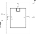
図1は、第1の実施形態の半導体装置の模式平面図である。図2は、第1の実施形態の半導体装置の模式断面図である。図2は図1のAA’断面図である。以下、第一導電型がp型、第二導電型がn型である場合を例に説明する。 FIG. 1 is a schematic plan view of the semiconductor device of the first embodiment. FIG. 2 is a schematic cross-sectional view of the semiconductor device of the first embodiment. FIG. 2 is a cross-sectional view taken along the line AA'of FIG. Hereinafter, a case where the first conductive type is the p-type and the second conductive type is the n-type will be described as an example.
第1の実施形態の半導体装置は、半導体層に形成されたトレンチの中にゲート電極を備えるトレンチゲート型のIGBT100である。以下、第一導電型がp型、第二導電型がn型である場合を例に説明する。 The semiconductor device of the first embodiment is a trench gate type IGBT 100 having a gate electrode in a trench formed in a semiconductor layer. Hereinafter, a case where the first conductive type is the p-type and the second conductive type is the n-type will be described as an example.
第1の実施形態のIGBT100は、セル領域101、セル端領域102、終端領域103、第1のゲート電極パッド111、第2のゲート電極パッド112を備える。IGBT100は、半導体層10、エミッタ電極12、コレクタ電極14を備える。
The IGBT 100 of the first embodiment includes a
半導体層10の中には、メイントレンチ20(第1のトレンチ)、コントロールトレンチ22(第2のトレンチ)、メインゲート電極24(第1のゲート電極)、コントロールゲート電極26(第2のゲート電極)、p型コレクタ領域28(第一導電型コレクタ領域)、n型バッファ領域30、n型ドリフト領域32(第二導電型ドリフト領域)、p型ベース領域34(第一導電型ベース領域)、第1のn型エミッタ領域36(第1の第二導電型エミッタ領域)、第2のn型エミッタ領域37(第2の第二導電型エミッタ領域)、p型周辺領域38、p型ガードリング領域40、ゲート絶縁膜42、周辺トレンチ44、トレンチ電極46が設けられる。
In the
半導体層10は、第1の面P1と、第1の面P1に対向する第2の面P2とを有する。半導体層10は、例えば、単結晶シリコンである。半導体層10の膜厚は、例えば、40μm以上700μm以下である。
The
エミッタ電極12は、半導体層10の第1の面P1の側に設けられる。エミッタ電極12は、例えば、セル領域101の全面を覆う。エミッタ電極12の少なくとも一部は半導体層10の第1の面P1に接する。エミッタ電極12は、例えば、金属である。エミッタ電極12には、エミッタ電圧が印加される。エミッタ電圧は、例えば、0Vである。
The
コレクタ電極14は、半導体層10の第2の面P2の側に設けられる。コレクタ電極14の少なくとも一部は半導体層10の第2の面P2に接する。コレクタ電極14は、例えば、金属である。コレクタ電極14には、コレクタ電圧が印加される。コレクタ電圧は、例えば、200V以上6500V以下である。
The collector electrode 14 is provided on the side of the second surface P2 of the
第1のゲート電極パッド111は、半導体層10の第1の面P1の側に設けられる。第1のゲート電極パッド111は、セル領域101のメインゲート電極24に電気的に接続さる。第1のゲート電極パッド111には、第1のゲート電圧が印加される。
The first
第2のゲート電極パッド112は、半導体層10の第1の面P1の側に設けられる。第2のゲート電極パッド112は、セル端領域102のコントロールゲート電極26に電気的に接続さる。第2のゲート電極パッド112には、第2のゲート電圧が印加される。
The second
セル端領域102は、セル領域101の端部に設けられる。セル端領域102は、セル領域101に隣り合って設けられる。セル端領域102は、例えば、セル領域101の両側の端部に隣り合って設けられる。終端領域103は、セル領域101とセル端領域102の周囲に設けられる。終端領域103は、セル領域101とセル端領域102を囲む。
The
セル領域101は主にIGBT100のオン状態にて電流を流す機能を有する。セル端領域102は、IGBT100のターンオフ動作の際に電流集中を緩和する機能を有する。終端領域103は、IGBT100がオフ状態つまり逆バイアス時、IGBT100の耐圧の低下を抑制する機能を有する。
The
セル領域101は、エミッタ電極12、コレクタ電極14、メイントレンチ20、メインゲート電極24、p型コレクタ領域28、n型バッファ領域30、n型ドリフト領域32、p型ベース領域34、第1のn型エミッタ領域36、ゲート絶縁膜42を有する。
The
セル端領域102は、エミッタ電極12、コレクタ電極14、コントロールトレンチ22、コントロールゲート電極26、p型コレクタ領域28、n型バッファ領域30、n型ドリフト領域32、p型ベース領域34、第2のn型エミッタ領域37、ゲート絶縁膜42を有する。
The
終端領域103は、エミッタ電極12、コレクタ電極14、p型コレクタ領域28、n型バッファ領域30、n型ドリフト領域32、p型周辺領域38、p型ガードリング領域40、ゲート絶縁膜42、周辺トレンチ44、トレンチ電極46を有する。
The
p型コレクタ領域28は、p+型の半導体領域である。p型コレクタ領域28は、コレクタ電極14に電気的に接続される。p型コレクタ領域28は、コレクタ電極14に接する。
The p-
p型コレクタ領域28は、IGBT100のオン状態の際に正孔の供給源となる。
The p-
n型バッファ領域30は、n型の半導体領域である。n型バッファ領域30は、第1の面P1とp型コレクタ領域28との間に設けられる。n型バッファ領域30は、IGBT100のオフ状態の際に、空乏層の伸びを抑制する機能を有する。n型バッファ領域30を設けない構成とすることも可能である。
The n-type buffer region 30 is an n-type semiconductor region. The n-type buffer area 30 is provided between the first surface P1 and the p-
n型ドリフト領域32は、n−型の半導体領域である。n型ドリフト領域32は、第1の面P1とn型バッファ領域30との間に設けられる。n型ドリフト領域32のn型不純物濃度は、n型バッファ領域30のn型不純物濃度より低い。
The n-
n型ドリフト領域32は、IGBT100のオン状態の際にオン電流の経路となる。n型ドリフト領域32は、IGBT100のオフ状態の際に空乏化し、IGBT100の耐圧を維持する機能を有する。
The n-
p型ベース領域34は、p型の半導体領域である。p型ベース領域34は、第1の面P1とn型ドリフト領域32との間に設けられる。p型ベース領域34の第1の面P1から第2の面P2に向かう方向の深さは、例えば、6μm以下である。p型ベース領域34は、メインゲート電極24に、セル領域101のトランジスタの閾値電圧を超える電圧が印加されたIGBT100のオン状態の際にn型反転層が形成され、トランジスタのチャネル領域として機能する。
The p-
第1のn型エミッタ領域36は、n+型の半導体領域である。第1のn型エミッタ領域36は、セル領域101に設けられる。第1のn型エミッタ領域36は、第1の面P1とp型ベース領域34との間に設けられる。第1のn型エミッタ領域36のn型不純物濃度は、n型ドリフト領域32のn型不純物濃度より高い。
The first n-
第1のn型エミッタ領域36は、エミッタ電極12に電気的に接続される。第1のn型エミッタ領域36は、エミッタ電極12に接する。第1のn型エミッタ領域36は、IGBT100のオン状態の際に電子の供給源となる。
The first n-
メイントレンチ20は、セル領域101に設けられる。メイントレンチ20は、例えば、第1の面P1に略平行な第1の方向に伸長するストライプ形状を有する。
The main trench 20 is provided in the
メイントレンチ20は、p型ベース領域34を貫通する。メイントレンチ20の第1の面P1から第2の面P2に向かう方向の深さは、例えば、6μm以下である。
The main trench 20 penetrates the p-
メインゲート電極24は、メイントレンチ20の中に設けられる。メインゲート電極24は、例えば、n型不純物又はp型不純物を含む多結晶シリコンである。メインゲート電極24は、図示しない配線層を用いて、第1のゲート電極パッド111に電気的に接続される。
The
メインゲート電極24とp型ベース領域34の間には、ゲート絶縁膜42が設けられる。ゲート絶縁膜42は、例えば、酸化シリコン膜である。
A
第2のn型エミッタ領域37は、n+型の半導体領域である。第2のn型エミッタ領域37は、セル端領域102に設けられる。第2のn型エミッタ領域37は、第1の面P1とp型ベース領域34との間に設けられる。第2のn型エミッタ領域37のn型不純物濃度は、n型ドリフト領域32のn型不純物濃度より高い。第2のn型エミッタ領域37は、例えば、第1のn型エミッタ領域36と同一の深さ、及び、同一のn型不純物濃度を有してもよい。
The second n-
第2のn型エミッタ領域37は、エミッタ電極12に電気的に接続される。第2のn型エミッタ領域37は、エミッタ電極12に接する。第2のn型エミッタ領域37は、IGBT100のオン状態の際に電子の供給源となる。
The second n-
コントロールトレンチ22は、セル端領域102に設けられる。コントロールトレンチ22は、例えば、第1の面P1に略平行な第1の方向に伸長するストライプ形状を有する。
The
コントロールトレンチ22は、p型ベース領域34を貫通する。コントロールトレンチ22の第1の面P1から第2の面P2に向かう方向の深さは、例えば、6μm以下である。
The
コントロールトレンチ22は、メイントレンチ20と同一の形状を有していてもよい。コントロールトレンチ22は、メイントレンチ20と同一のピッチで配置されてもよい。
The
コントロールゲート電極26は、コントロールトレンチ22の中に設けられる。コントロールゲート電極26は、例えば、n型不純物又はp型不純物を含む多結晶シリコンである。コントロールゲート電極26は、図示しない配線層を用いて、第2のゲート電極パッド112に電気的に接続される。
The
コントロールゲート電極26とp型ベース領域34の間には、ゲート絶縁膜42が設けられる。ゲート絶縁膜42は、例えば、酸化シリコン膜である。
A
p型周辺領域38は、p型の半導体領域である。p型周辺領域38は、終端領域103に設けられる。p型周辺領域38は、第1の面P1とn型ドリフト領域32との間に設けられる。p型周辺領域38は、例えば、セル領域101とセル端領域102とを囲んで設けられる。p型周辺領域38は、例えば、p型ベース領域34に接する。
The p-type peripheral region 38 is a p-type semiconductor region. The p-type peripheral region 38 is provided in the
p型周辺領域38の第1の面P1から第2の面P2に向かう方向の深さは、例えば、p型ベース領域34の第1の面P1から第2の面P2に向かう方向の深さよりも深い。p型周辺領域38の第1の面P1から第2の面P2に向かう方向の深さは、例えば、6μm以上12μm以下である。
The depth in the direction from the first surface P1 to the second surface P2 of the p-type peripheral region 38 is, for example, greater than the depth in the direction from the first surface P1 to the second surface P2 of the p-
p型周辺領域38は、オフ状態の際のセル領域101及びセル端領域102の端部での電界強度を緩和する機能を有する。
The p-type peripheral region 38 has a function of relaxing the electric field strength at the ends of the
周辺トレンチ44は、p型周辺領域38の中に設けられる。トレンチ電極46は、周辺トレンチ44中に設けられる。トレンチ電極46は、例えば、n型不純物又はp型不純物を含む多結晶シリコンである。トレンチ電極46は、例えば、フローティングである。トレンチ電極46とp型周辺領域38の間には、ゲート絶縁膜42が設けられる。なお、周辺トレンチ44を設けない構成とすることも可能である。
The
p型ガードリング領域40は、終端領域103に設けられる。p型ガードリング領域40は、第1の面P1とn型ドリフト領域32との間に設けられる。p型ガードリング領域40は、セル領域101とセル端領域102とを囲んで設けられる。p型ガードリング領域40は、フローティングである。p型ガードリング領域40の第1の面P1から第2の面P2に向かう方向の深さは、例えば、p型ベース領域34の第1の面P1から第2の面P2に向かう方向の深さよりも深い。
The p-type
p型ガードリング領域40は、IGBT100がオフ状態の際のセル領域101及びセル端領域102の端部での電界強度を緩和する機能を有する。
The p-type
IGBT100は、セル領域101のメインゲート電極24と、セル端領域102のコントロールゲート電極26が電気的に分離されている。メインゲート電極24には、第1のゲート電極パッド111から第1のゲート電圧を印加することができる。コントロールゲート電極26には、第2のゲート電極パッド112から第2のゲート電圧を印加することができる。
In the
第1のゲート電圧と第2のゲート電圧は、異なるタイミングで印加することが可能である。また、第1のゲート電圧と第2のゲート電圧を異なる電圧とすることも可能である。 The first gate voltage and the second gate voltage can be applied at different timings. It is also possible that the first gate voltage and the second gate voltage are different voltages.
次に、IGBT100の動作について説明する。
Next, the operation of the
IGBT100のオフ状態では、エミッタ電極12には、エミッタ電圧が印加される。エミッタ電圧は、例えば、0Vである。コレクタ電極14には、コレクタ電圧が印加される。コレクタ電圧は、例えば、200V以上6500V以下である。
When the
IGBT100をターンオン動作させて、オン状態にする際に、第1のゲート電極パッド111、及び、第2のゲート電極パッド112にターンオン電圧を印加する。メインゲート電極24、及び、コントロールゲート電極26にもターンオン電圧が印加される。
When the
ここで、ターンオン電圧とは、セル領域101、及び、セル端領域102のトランジスタの閾値電圧を超える電圧である。ターンオン電圧は、例えば、15Vである。セル領域101のトランジスタと、セル端領域102のトランジスタの両方のトランジスタがオン状態になる。
Here, the turn-on voltage is a voltage that exceeds the threshold voltage of the transistor in the
次に、IGBT100をターンオフ動作させて、オフ状態にする際に、最初に第2のゲート電極パッド112にターンオフ電圧を印加する。したがって、コントロールゲート電極26にもターンオフ電圧が印加される。ここで、ターンオフ電圧とはセル領域101、及び、セル端領域102のトランジスタがオン状態とならない閾値以下の電圧であり、例えば、0Vである。セル端領域102のトランジスタが、セル領域101のトランジスタに先行してオフ状態になる。
Next, when the
次に、第1のゲート電極パッド111に、ターンオフ電圧を印加する。メインゲート電極24にもターンオフ電圧が印加される。セル端領域102のトランジスタに続いて、セル領域101のトランジスタがオフ状態になり、IGBT100がオフ状態になる。ただし、セル領域101のトランジスタと、セル端領域102のトランジスタは明確に分離された構造ではないが、動作説明の便宜上、セル領域101のトランジスタ、セル端領域102のトランジスタという記載をするものとする。
Next, a turn-off voltage is applied to the first
次に、第1の実施形態の半導体装置の作用及び効果について説明する。 Next, the operation and effect of the semiconductor device of the first embodiment will be described.
IGBTのセルが形成されたセル領域の端部では、セルがオン状態の際にセルの存在しない終端領域の一部にまでキャリアが広がる。セルがオン状態からオフ状態に移行するターンオフ動作の際に、広がったキャリアがセル領域の端部に近いセルに集中して排出されるため電流密度が高くなる。このため、IGBTの破壊が生じるおそれがある。また、終端領域に広がったキャリアを排出するために時間がかかり、ターンオフ動作の際のスイッチング損失が大きくなるおそれがある。 At the end of the cell region where the cells of the IGBT are formed, the carriers extend to a part of the terminal region where the cells do not exist when the cells are on. During the turn-off operation in which the cell shifts from the on state to the off state, the spread carriers are concentrated and discharged to the cell near the end of the cell region, so that the current density becomes high. Therefore, the IGBT may be destroyed. In addition, it takes time to discharge the carriers spread in the terminal region, which may increase the switching loss during the turn-off operation.
図3は、比較形態の半導体装置の模式平面図である。図4は、比較形態の半導体装置の模式断面図である。図4は図3のBB’断面図である。 FIG. 3 is a schematic plan view of the semiconductor device in the comparative form. FIG. 4 is a schematic cross-sectional view of the semiconductor device of the comparative form. FIG. 4 is a cross-sectional view taken along the line BB'of FIG.
比較形態の半導体装置は、半導体層に形成されたトレンチの中にゲート電極を備えるトレンチゲート型のIGBT900である。
The semiconductor device of the comparative form is a trench
比較形態のIGBT900は、セル領域101、終端領域103、第1のゲート電極パッド111、を備える。IGBT900は、半導体層10、エミッタ電極12、コレクタ電極14を備える。
The comparative form of the
半導体層10の中には、メイントレンチ20、メインゲート電極24、p型コレクタ領域28、n型バッファ領域30、n型ドリフト領域32、p型ベース領域34、第1のn型エミッタ領域36、p型周辺領域38、p型ガードリング領域40、ゲート絶縁膜42、周辺トレンチ44、トレンチ電極46が設けられる。
In the
比較形態のIGBT900は、セル端領域102、及び、第2のゲート電極パッド112を備えない点で、第1の実施形態のIGBT100と異なる。また、比較形態のIGBT900は、コントロールトレンチ22、コントロールゲート電極26、第2のn型エミッタ領域37を備えない点で、第1の実施形態のIGBT100と異なる。
The
図5は、比較形態の半導体装置の作用の説明図である。図5は、比較形態のIGBT900のオン状態のキャリアの蓄積状態を示す図である。
FIG. 5 is an explanatory diagram of the operation of the semiconductor device in the comparative form. FIG. 5 is a diagram showing an accumulation state of carriers in the ON state of the
図5に示すように、終端領域103の一部にもキャリアが広がり、終端領域103の一部にもキャリアが多量に蓄積されている。
As shown in FIG. 5, carriers spread to a part of the
図6は、比較形態の半導体装置の作用の説明図である。図6は、比較形態のIGBT900のターンオフ動作時の電流の状態を示す図である。矢印が電流の流れを示す。矢印の太さが電流密度を示す。
FIG. 6 is an explanatory diagram of the operation of the semiconductor device in the comparative form. FIG. 6 is a diagram showing a state of current during the turn-off operation of the
IGBT900では、セル領域101のメインゲート電極24にターンオフ電圧が印加されると、セル領域101のトランジスタが一斉にオフ状態になる。
In the
終端領域103、特にp型ガードリング領域40の直上には、キャリアの排出経路が無い。このため、終端領域103の一部にも蓄積された多量のキャリアが、セル領域101の端部に集中する。したがって、セル領域101の端部の電流密度が高くなる。よって、IGBT900が破壊するおそれがある。また、IGBT900が破壊しなかったとしても、キャリアの排出に時間がかかり、ターンオフ動作の際のスイッチング損失が大きくなるおそれがある。
There is no carrier discharge path directly above the
図7は、第1の実施形態の半導体装置の作用及び効果の説明図である。図7は、第1の実施形態のIGBT100のオン状態のキャリアの蓄積状態を示す図である。
FIG. 7 is an explanatory diagram of the operation and effect of the semiconductor device of the first embodiment. FIG. 7 is a diagram showing an accumulation state of carriers in the ON state of the
図7に示すように、比較形態の場合と同様、終端領域103の一部にもキャリアが広がり、終端領域103の一部にもキャリアが多量に蓄積されている。
As shown in FIG. 7, as in the case of the comparative form, the carriers spread to a part of the
図8は、第1の実施形態の半導体装置の作用及び効果の説明図である。図8は、第1の実施形態のIGBT100をオフ状態にする際に、セル端領域102のトランジスタを、セル領域101のトランジスタに先行してオフ状態にした状態でのキャリアの蓄積状態を示す図である。
FIG. 8 is an explanatory diagram of the operation and effect of the semiconductor device of the first embodiment. FIG. 8 is a diagram showing a carrier accumulation state in a state where the transistor in the
セル端領域102のトランジスタは、オフ状態であるため、セル端領域102での電子の注入は遮断されている。したがって、図8に示すように、終端領域103及びセル端領域102のキャリアの蓄積量が、セル領域101の蓄積量よりも少なくなる。しかし、セル領域101はオン状態のため、IGBT100自体はオン状態にある。
Since the transistor in the
図9は、第1の実施形態の半導体装置の作用及び効果の説明図である。図9は、第1の実施形態のIGBT100の、ターンオフ動作時の電流の状態を示す図である。矢印が電流の流れを示す。矢印の太さが電流密度を示す。
FIG. 9 is an explanatory diagram of the operation and effect of the semiconductor device of the first embodiment. FIG. 9 is a diagram showing the current state of the
IGBT100では、セル端領域102のトランジスタがオフ状態になった後に、セル領域101のメインゲート電極24にターンオフ電圧が印加され、セル領域101のトランジスタがオフ状態となる。
In the
終端領域103及びセル端領域102のキャリアの蓄積量が、既に少なくなっているため、セル端領域102あるいはセル領域101の端部でのキャリアの集中は生じない。したがって、電流密度が高くなることがない。よって、IGBT100の破壊が抑制される。また、キャリアの排出に要する時間も短くなり、ターンオフ動作の際のスイッチング損失の増加が抑制される。
Since the accumulated amount of carriers in the
以上、第1の実施形態によれば、IGBT100の電流集中による破壊を抑制することが可能となる。また、ターンオフ動作の際のスイッチング損失の増加を抑制することが可能となる。
As described above, according to the first embodiment, it is possible to suppress the destruction of the
(第2の実施形態)
第2の実施形態の半導体装置は、セル端領域は、半導体層の中に設けられた第3のトレンチと、第3のトレンチの中に設けられ第1のゲート電極パッドに接続された第3のゲート電極と、を有する点で、第1の実施形態と異なる。以下、第1の実施形態と重複する内容については、一部記述を省略する。
(Second Embodiment)
In the semiconductor device of the second embodiment, the cell end region is connected to a third trench provided in the semiconductor layer and a third gate electrode pad provided in the third trench and connected to the first gate electrode pad. It differs from the first embodiment in that it has a gate electrode of. Hereinafter, some descriptions of the contents overlapping with the first embodiment will be omitted.
図10は、第2の実施形態の半導体装置の模式断面図である。図10は図1のAA’断面図に相当する断面図である。 FIG. 10 is a schematic cross-sectional view of the semiconductor device of the second embodiment. FIG. 10 is a cross-sectional view corresponding to the AA'cross-sectional view of FIG.
第2の実施形態の半導体装置は、半導体層に形成されたトレンチの中にゲート電極を備えるトレンチ型のIGBT200である。
The semiconductor device of the second embodiment is a
第2の実施形態のIGBT200は、セル領域101、セル端領域102、終端領域103、第1のゲート電極パッド111、第2のゲート電極パッド112を備える。IGBT200は、半導体層10、エミッタ電極12、コレクタ電極14を備える。
The
半導体層10の中には、メイントレンチ20(第1のトレンチ)、コントロールトレンチ22(第2のトレンチ)、メインゲート電極24(第1のゲート電極)、コントロールゲート電極26(第2のゲート電極)、p型コレクタ領域28、n型バッファ領域30、n型ドリフト領域32、p型ベース領域34、第1のn型エミッタ領域36、第2のn型エミッタ領域37、p型周辺領域38、p型ガードリング領域40、ゲート絶縁膜42、周辺トレンチ44、トレンチ電極46が設けられる。
In the
半導体層10の中には、更に、メイントレンチ23(第3のトレンチ)、メインゲート電極25(第3のゲート電極)が設けられる。
A main trench 23 (third trench) and a main gate electrode 25 (third gate electrode) are further provided in the
メイントレンチ23、及び、メインゲート電極25は、セル端領域102に設けられる。セル端領域102のメイントレンチ23、及び、メインゲート電極25は、例えば、2つのコントロールトレンチ22の間に設けられる。
The main trench 23 and the
メインゲート電極25は、第1のゲート電極パッド111に電気的に接続される。したがって、セル端領域102内に、一部、セル領域101のトランジスタと同じ動作をするトランジスタが設けられる。
The
第2の実施形態のIGBT200によれば、セル端領域102に、セル領域101のトランジスタと同じ動作をするトランジスタを設けることにより、終端領域103のキャリアの蓄積量を調整することが可能となる。したがって、IGBT200の特性の最適化を図ることが容易になる。
According to the
以上、第2の実施形態によれば、IGBT200の電流集中による破壊を抑制することが可能となる。また、ターンオフ動作の際のスイッチング損失の増加を抑制することが可能となる。更に、IGBT200の特性の最適化を図ることが容易になる。
As described above, according to the second embodiment, it is possible to suppress the destruction of the
なお図10では、コントロールトレンチ22の間にメイントレンチ23を配置しているが、コントロールトレンチ22とメイントレンチ23の配置は自由に変えられる。
Although the main trench 23 is arranged between the
(第3の実施形態)
第3の実施形態の半導体装置は、セル領域は、半導体層の中に設けられコレクタ電極に接するp型コレクタ領域と、p型コレクタ領域と第1の面との間に設けられたn型ドリフト領域と、n型ドリフト領域と第1の面との間に設けられたp型ベース領域と、p型ベース領域と第1の面との間に設けられエミッタ電極に接するn型エミッタ領域と、を有し、セル端領域は、p型コレクタ領域と、n型ドリフト領域と、n型ドリフト領域と第1の面との間に設けられたp型領域と、を有する。
(Third Embodiment)
In the semiconductor device of the third embodiment, the cell region is a p-type collector region provided in the semiconductor layer and in contact with the collector electrode, and an n-type drift provided between the p-type collector region and the first surface. A p-type base region provided between the region, the n-type drift region and the first surface, and an n-type emitter region provided between the p-type base region and the first surface and in contact with the emitter electrode. The cell end region has a p-type collector region, an n-type drift region, and a p-type region provided between the n-type drift region and the first surface.
第3の実施形態の半導体装置は、セル端領域にエミッタ領域が設けられない点で、第1の実施形態と異なっている。以下、第1の実施形態と重複する内容については、一部記述を省略する。 The semiconductor device of the third embodiment is different from the first embodiment in that an emitter region is not provided in the cell end region. Hereinafter, some descriptions of the contents overlapping with the first embodiment will be omitted.
図11は、第3の実施形態の半導体装置の模式平面図である。図12は、第3の実施形態の半導体装置の模式断面図である。図12は図11のCC’断面図である。 FIG. 11 is a schematic plan view of the semiconductor device of the third embodiment. FIG. 12 is a schematic cross-sectional view of the semiconductor device of the third embodiment. FIG. 12 is a cross-sectional view of CC'of FIG.
第3の実施形態の半導体装置は、半導体層に形成されたトレンチの中にゲート電極を備えるトレンチゲート型のIGBT300である。
The semiconductor device of the third embodiment is a trench
第3の実施形態のIGBT300は、セル領域101、セル端領域102、終端領域103、第1のゲート電極パッド111、第2のゲート電極パッド112を備える。IGBT300は、半導体層10、エミッタ電極12、コレクタ電極14を備える。
The
半導体層10の中には、メイントレンチ20(第1のトレンチ)、コントロールトレンチ122(第2のトレンチ)、メインゲート電極24(第1のゲート電極)、コントロールゲート電極126(第2のゲート電極)、p型コレクタ領域28、n型バッファ領域30、n型ドリフト領域32、p型ベース領域34、n型エミッタ領域136、p型領域138((第一導電型領域))、p型ガードリング領域40、ゲート絶縁膜42が設けられる。
In the
第1のゲート電極パッド111は、半導体層10の第1の面P1の側に設けられる。第1のゲート電極パッド111は、セル領域101のメインゲート電極24に電気的に接続さる。第1のゲート電極パッド111には、第1のゲート電圧が印加される。
The first
第2のゲート電極パッド112は、半導体層10の第1の面P1の側に設けられる。第2のゲート電極パッド112は、セル端領域102のコントロールゲート電極126に電気的に接続さる。第2のゲート電極パッド112には、第2のゲート電圧が印加される。
The second
セル領域101は、エミッタ電極12、コレクタ電極14、メイントレンチ20、メインゲート電極24、p型コレクタ領域28、n型バッファ領域30、n型ドリフト領域32、p型ベース領域34、n型エミッタ領域136、ゲート絶縁膜42を有する。セル領域101の構成は、第1の実施形態のIGBT100と同様である。
The
セル端領域102は、エミッタ電極12、コレクタ電極14、コントロールトレンチ122、コントロールゲート電極126、p型コレクタ領域28、n型バッファ領域30、n型ドリフト領域32、ゲート絶縁膜42、p型領域138を有する。セル端領域102には、n型エミッタ領域が存在しない。
The
終端領域103は、コレクタ電極14、p型コレクタ領域28、n型バッファ領域30、n型ドリフト領域32、p型ガードリング領域40を有する。
The
n型エミッタ領域136は、n+型の半導体領域である。n型エミッタ領域136は、セル領域101に設けられる。n型エミッタ領域136は、第1の面P1とp型ベース領域34との間に設けられる。n型エミッタ領域136のn型不純物濃度は、n型ドリフト領域32のn型不純物濃度より高い。
The n-
n型エミッタ領域136は、エミッタ電極12に電気的に接続される。n型エミッタ領域136は、エミッタ電極12に接する。n型エミッタ領域136は、IGBT300のオン状態の際に電子の供給源となる。
The n-
メイントレンチ20は、セル領域101に設けられる。メイントレンチ20は、例えば、第1の面P1に略平行な第1の方向に伸長する。
The main trench 20 is provided in the
メインゲート電極24は、メイントレンチ20の中に設けられる。メインゲート電極24は、図示しない配線層を用いて、第1のゲート電極パッド111に電気的に接続される。
The
p型領域138は、p型の半導体領域である。p型領域138は、セル端領域102に設けられる。p型領域138は、第1の面P1とn型ドリフト領域32との間に設けられる。p型領域138は、例えば、セル領域101を囲んで設けられる。p型領域138は、p型ベース領域34に接する。p型領域138は、例えば、エミッタ電極12に接する。
The p-
p型領域138の第1の面P1から第2の面P2に向かう方向の深さ(図12中のd2)は、例えば、p型ベース領域34の第1の面P1から第2の面P2に向かう方向の深さ(図12中のd1)よりも深い。p型領域138の第1の面P1から第2の面P2に向かう方向の深さd1は、例えば、6μm以上12μm以下である。
The depth in the direction from the first surface P1 to the second surface P2 of the p-type region 138 (d2 in FIG. 12) is, for example, the first surface P1 to the second surface P2 of the p-
コントロールトレンチ122は、セル端領域102に設けられる。コントロールトレンチ22は、例えば、第1の面P1に略平行な第1の方向に伸長する。
The
コントロールトレンチ122は、p型領域138内に設けられる。コントロールトレンチ22の第1の面P1から第2の面P2に向かう方向の深さ(図12中のd3)は、p型領域138の第1の面P1から第2の面P2に向かう方向の深さd2よりも浅い。コントロールトレンチ22の第1の面P1から第2の面P2に向かう方向の深さd3は、例えば、4μm以上6μm以下である。
The
隣りあう2個のコントロールトレンチ122の間隔(図12中のs2)は、隣り合う2個のメイントレンチ20の間隔(図12中のs1)より大きくても小さくても良い。あるいは、等しくても良い。 The distance between the two adjacent control trenches 122 (s2 in FIG. 12) may be larger or smaller than the distance between the two adjacent main trenches 20 (s1 in FIG. 12). Alternatively, they may be equal.
コントロールゲート電極126は、コントロールトレンチ122の中に設けられる。コントロールゲート電極126は、図示しない配線層を用いて、第2のゲート電極パッド112に電気的に接続される。
The
コントロールゲート電極126とp型領域138の間には、ゲート絶縁膜42が設けられる。
A
第1の実施形態のIGBT100と異なり、セル端領域102には、トランジスタは形成されない。
Unlike the
次に、IGBT300の動作について説明する。
Next, the operation of the
IGBT300のオフ状態では、例えば、エミッタ電極12には、エミッタ電圧が印加される。エミッタ電圧は、例えば、0Vである。コレクタ電極14には、コレクタ電圧が印加される。コレクタ電圧は、例えば、200V以上6500V以下である。
In the off state of the
第1のゲート電極パッド111、及び、第2のゲート電極パッド112には、ターンオフ電圧が印加されている。メインゲート電極24、及び、コントロールゲート電極126にもターンオフ電圧が印加されている。ターンオフ電圧はセル領域101のトランジスタがオン状態とならない閾値以下の電圧であり、例えば、0Vである。
A turn-off voltage is applied to the first
IGBT300をターンオン動作させて、オン状態にする際に、第1のゲート電極パッド111にターンオン電圧を印加する。メインゲート電極24にもターンオン電圧が印加される。
When the
ターンオン電圧とは、セル領域101のトランジスタの閾値電圧を超える電圧である。ターンオン電圧は、例えば、15Vである。セル領域101のトランジスタがオン状態になる。なお、セル端領域102には、トランジスタが形成されていないため、トランジスタ動作は生じない。
The turn-on voltage is a voltage that exceeds the threshold voltage of the transistor in the
IGBT300をターンオフ動作させて、オフ状態にする際に、最初に第2のゲート電極パッド112に負電位を印加する。コントロールゲート電極126にも負電位が印加される。セル端領域102のコントロールトレンチ122の周囲のp型領域138に、p型蓄積層が形成される。
When the
次に、第1のゲート電極パッド111に、ターンオフ電圧を印加する。メインゲート電極24にもターンオフ電圧が印加される。セル領域101のトランジスタがオフ状態になりし、IGBT300がオフ状態になる。
Next, a turn-off voltage is applied to the first
第2のゲート電極パッド112に負電位を印加するのと、第1のゲート電極パッド111にターンオフ電圧を印加するのは同時でもよい。第1のゲート電極パッド111にターンオフ電圧を印加したあとに、第2のゲート電極パッド112に負電位を印加してもよい。第2のゲート電極パッド112に負電位を印加したあとに、第1のゲート電極パッド111にターンオフ電圧を印加してもよい。
The negative potential may be applied to the second
次に、第3の実施形態の半導体装置の作用及び効果について説明する。 Next, the operation and effect of the semiconductor device of the third embodiment will be described.
図13は、第3の実施形態の半導体装置の作用及び効果の説明図である。図13は、第3の実施形態のIGBT300のオン状態のキャリアの蓄積状態を示す図である。
FIG. 13 is an explanatory diagram of the operation and effect of the semiconductor device of the third embodiment. FIG. 13 is a diagram showing an accumulation state of carriers in the ON state of the
図13に示すように、終端領域103の一部にもキャリアが広がり、終端領域103の一部にもキャリアが多量に蓄積されている。
As shown in FIG. 13, carriers spread to a part of the
図14は、第3の実施形態の半導体装置の作用及び効果の説明図である。図14は、第3の実施形態のIGBT300において、セル端領域102のコントロールゲート電極126に負電圧を印加し、p型領域138にp型蓄積層を形成した状態でのキャリアの蓄積状態を示す。
FIG. 14 is an explanatory diagram of the operation and effect of the semiconductor device of the third embodiment. FIG. 14 shows a carrier accumulation state in a state in which a negative voltage is applied to the
p型領域138にp型蓄積層が形成されることで、セル端領域102からのキャリアの排出が促進される。したがって、図14に示すように、終端領域103及びセル端領域102のキャリアの蓄積量が、セル領域101の蓄積量よりも少なくなる。
The formation of the p-type storage layer in the p-
図15は、第3の実施形態の半導体装置の作用及び効果の説明図である。図15は、第3の実施形態のIGBT300のターンオフ動作時の電流の状態を示す図である。矢印が電流の流れを示す。矢印の太さが電流密度を示す。
FIG. 15 is an explanatory diagram of the operation and effect of the semiconductor device of the third embodiment. FIG. 15 is a diagram showing a state of current during the turn-off operation of the
IGBT300では、コントロールゲート電極126に負電位を印加し、セル端領域102のp型領域138にp型蓄積層を形成する。セル領域101のメインゲート電極24にターンオフ電圧が印加され、セル領域101のトランジスタがオフ状態になる。
In the
セル端領域102はp型領域138にp型蓄積層を形成しているためキャリアの排出が効果的に行われるためセル端領域102あるいはセル領域101の端部のキャリアの集中は生じない。したがって、電流密度が高くなることがない。よって、IGBT300の破壊が抑制される。また、キャリアの排出に要する時間も短くなり、ターンオフ動作の際のスイッチング損失の増加が抑制される。
Since the
p型領域138にp型蓄積層を数多く形成するためには、隣りあう2個のコントロールトレンチ122の間隔s2が、隣り合う2個のメイントレンチ20の間隔s1よりも狭いことが好ましい。
In order to form a large number of p-type storage layers in the p-
以上、第3の実施形態によれば、IGBT300の電流集中による破壊を抑制することが可能となる。また、ターンオフ動作の際のスイッチング損失の増加を抑制することが可能となる。
As described above, according to the third embodiment, it is possible to suppress the destruction of the
(第4の実施形態)
第4の実施形態の半導体装置は、隣りあう2個の第2のトレンチの間にn型領域が設けられた点で、第3の実施形態と異なる。以下、第3の実施形態と重複する内容については、一部記述を省略する。
(Fourth Embodiment)
The semiconductor device of the fourth embodiment is different from the third embodiment in that an n-type region is provided between two adjacent second trenches. Hereinafter, some descriptions of the contents overlapping with the third embodiment will be omitted.
図16は、第4の実施形態の半導体装置の模式断面図である。図16は、図11のCC’断面図に相当する断面図である。 FIG. 16 is a schematic cross-sectional view of the semiconductor device of the fourth embodiment. FIG. 16 is a cross-sectional view corresponding to the CC'cross-sectional view of FIG.
第4の実施形態の半導体装置は、半導体層に形成されたトレンチの中にゲート電極を備えるトレンチ型のIGBT400である。
The semiconductor device of the fourth embodiment is a
第4の実施形態のIGBT400は、セル領域101、セル端領域102、終端領域103、第1のゲート電極パッド111、第2のゲート電極パッド112を備える。IGBT400は、半導体層10、エミッタ電極12、コレクタ電極14を備える。
The
半導体層10の中には、メイントレンチ20(第1のトレンチ)、コントロールトレンチ122(第2のトレンチ)、メインゲート電極24(第1のゲート電極)、コントロールゲート電極126(第2のゲート電極)、p型コレクタ領域28、n型バッファ領域30、n型ドリフト領域32、p型ベース領域34、n型エミッタ領域136、p型領域138、p型ガードリング領域40、ゲート絶縁膜42、n型領域50(第二導電型領域)が設けられる。
In the
n型領域50は、セル端領域102に設けられる。n型領域50は、n型の半導体領域である。n型領域50は、2個のコントロールトレンチ122の間に設けられる。n型領域50は、上下をp型領域138に挟まれる。
The n-
n型領域50をもうけることより、疑似的に、コントロールゲート電極126をゲート電極とするpチャネル型MOSFET(Metal Oxide Field Effect Transistor)がセル端領域102に形成される。n型領域50は、pチャネル型MOSFETのチャネル領域として機能する。
By providing the n-
次に、IGBT400の動作について説明する。
Next, the operation of the
IGBT400のオフ状態では、例えば、エミッタ電極12には、エミッタ電圧が印加される。エミッタ電圧は、例えば、0Vである。コレクタ電極14には、コレクタ電圧が印加される。コレクタ電圧は、例えば、200V以上6500V以下である。
In the off state of the
第1のゲート電極パッド111には、ターンオフ電圧が印加されている。メインゲート電極24にもターンオフ電圧が印加されている。
A turn-off voltage is applied to the first
IGBT400をターンオン動作させて、オン状態にする際に、第1のゲート電極パッド111にターンオン電圧を印加する。メインゲート電極24にもターンオン電圧が印加される。コントロールゲート電極126には0Vもしくはメインゲート電極24と同じ電圧を印加する。
When the
ターンオン電圧は、セル領域101のトランジスタの閾値電圧を超える電圧である。ターンオン電圧は、例えば、15Vである。セル領域101のトランジスタがオン状態になる。なお、セル端領域102に形成されているpチャネル型MOSFETは、オフ状態である。このため、セル端領域102でのキャリアの排出は抑制される。
The turn-on voltage is a voltage that exceeds the threshold voltage of the transistor in the
IGBT400をターンオフ動作させて、オフ状態にする際に、第2のゲート電極パッド112に負電位を印加する。コントロールゲート電極126には負電位の電圧が印加される。このため、セル端領域102のコントロールトレンチ122の周囲のp型領域138にp型蓄積層が形成される。また、セル端領域102に形成されているpチャネル型MOSFETはオン状態となる。
When the
第1のゲート電極パッド111に、ターンオフ電圧を印加する。メインゲート電極24にもターンオフ電圧が印加される。セル領域101のトランジスタがオフ状態になり、IGBT400がオフ状態になる。
A turn-off voltage is applied to the first
IGBT400が、オン状態の際には、第3の実施形態と同様、終端領域103の一部にもキャリアが広がり、終端領域103の一部にもキャリアが多量に蓄積されている。セル端領域102に形成されているpチャネル型MOSFETは、オフ状態にある。このため、セル端領域102でのキャリアの排出は抑制される。したがって、第3の実施形態と比較して、オン抵抗は低減される。
When the
IGBT400を、オフ状態にする際に、セル端領域102のコントロールトレンチ122に負電圧を印加すると、p型領域138にp型蓄積層が形成される。また、セル端領域102に形成されているpチャネル型MOSFETもオン状態になる。
When a negative voltage is applied to the
pチャネル型MOSFETがオン状態になり、p型領域138にp型蓄積層が形成されることで、セル端領域102からのキャリアの排出が行われる。したがって、終端領域103及びセル端領域102のキャリアの蓄積量が、セル領域101の蓄積量よりも少なくなる。
When the p-channel MOSFET is turned on and the p-type storage layer is formed in the p-
セル領域101のメインゲート電極24にターンオフ電圧が印加され、セル領域101のトランジスタがオフ状態になる。終端領域103及びセル端領域102の下でのキャリアの蓄積量が、既に少なくなっているため、セル端領域102あるいはセル領域101の端部のキャリアの集中は生じない。したがって、電流密度が高くなることがない。よって、IGBT400の破壊が抑制される。また、キャリアの排出に要する時間も短くなり、ターンオフ動作の際のスイッチング損失の増加が抑制される。
A turn-off voltage is applied to the
以上、第4の実施形態によれば、IGBT400の電流集中による破壊を抑制することが可能となる。また、ターンオフ動作の際のスイッチング損失の増加を抑制することが可能となる。また、第3の実施形態と比較してオン抵抗が低減する。 なお、第1のゲート電極パッド111にターンオフ電圧を印加するのと、第2のゲート電極パッド112に負電位の電圧を印加するのとは、同時でもよい。
As described above, according to the fourth embodiment, it is possible to suppress the destruction of the
(第5の実施形態)
第5の実施形態の半導体装置は、p型領域の第1の面から第2の面に向かう方向の深さが、第2のトレンチの方向の深さよりも浅く、p型領域の第1の面から第2の面に向かう方向の深さが、p型ベース領域の第1の面から第2の面に向かう方向の深さと略同一である点で、第3の実施形態と異なる。以下、第3の実施形態と重複する内容については、一部記述を省略する。
(Fifth Embodiment)
In the semiconductor device of the fifth embodiment, the depth in the direction from the first surface to the second surface of the p-type region is shallower than the depth in the direction of the second trench, and the depth in the direction of the second trench is shallower than the depth in the direction of the second trench. It differs from the third embodiment in that the depth in the direction from the surface to the second surface is substantially the same as the depth in the direction from the first surface to the second surface of the p-type base region. Hereinafter, some descriptions of the contents overlapping with the third embodiment will be omitted.
図17は、第5の実施形態の半導体装置の模式断面図である。図17は、図11のCC’断面図に相当する断面図である。 FIG. 17 is a schematic cross-sectional view of the semiconductor device of the fifth embodiment. FIG. 17 is a cross-sectional view corresponding to the CC'cross-sectional view of FIG.
第5の実施形態の半導体装置は、半導体層に形成されたトレンチの中にゲート電極を備えるトレンチ型のIGBT500である。
The semiconductor device of the fifth embodiment is a
第5の実施形態のIGBT500は、セル領域101、セル端領域102、終端領域103、第1のゲート電極パッド111、第2のゲート電極パッド112を備える。IGBT500は、半導体層10、エミッタ電極12、コレクタ電極14を備える。
The
半導体層10の中には、メイントレンチ20(第1のトレンチ)、コントロールトレンチ122(第2のトレンチ)、メインゲート電極24(第1のゲート電極)、コントロールゲート電極126(第2のゲート電極)、p型コレクタ領域28、n型バッファ領域30、n型ドリフト領域32、p型ベース領域34、n型エミッタ領域136、p型領域138、p型ガードリング領域40、ゲート絶縁膜42が設けられる。
In the
p型領域138の第1の面P1から第2の面P2に向かう方向の深さ(図17中のd2)が、コントロールトレンチ122の第1の面P1から第2の面P2に向かう方向の深さ(図17中のd3)よりも浅い。コントロールトレンチ122は、p型領域138を突き抜け、n型ドリフト領域32に達している。
The depth of the p-shaped
また、p型領域138の第1の面P1から第2の面P2に向かう方向の深さd2は、p型ベース領域34の第1の面P1から第2の面P2に向かう方向の深さ(図17中のd1)と略同一である。
Further, the depth d2 in the direction from the first surface P1 to the second surface P2 of the p-
また、p型ガードリング領域40の第1の面P1から第2の面P2に向かう方向の深さも、p型ベース領域34の第1の面P1から第2の面P2に向かう方向の深さd1と略同一である。
Further, the depth of the p-type
第5の実施形態のIGBT500では、コントロールトレンチ122は、p型領域138を突き抜けている。このため、コントロールトレンチ122の周囲のp型領域138にp型蓄積層が形成された際の、セル端領域102からのキャリアの排出が促進される。したがって、IGBT500の破壊が更に抑制される。また、キャリアの排出に要する時間も更に短くなり、ターンオフ動作の際のスイッチング損失の増加が抑制される。
In the
また、IGBT500では、p型領域138やp型ガードリング領域40の深さが第3の実施形態のIGBT300よりも浅い。したがって、例えば、p型不純物拡散のための長時間の熱工程が不要となる。したがって、低コストで製造することが可能となる。また、例えば、低温プロセスで製造されるロジックデバイスやメモリデバイスとの同一チップへの混載が容易となる。
Further, in the
以上、第5の実施形態によれば、IGBT500の電流集中による破壊を更に抑制することが可能となる。また、ターンオフ動作の際のスイッチング損失の増加を更に抑制することが可能となる。また、低コストで製造が可能となる。また、ロジックデバイスやメモリデバイスとの同一チップへの混載が容易となる。
As described above, according to the fifth embodiment, it is possible to further suppress the destruction of the
第1ないし第5の実施形態においては、半導体層が単結晶シリコンである場合を例に説明したが、半導体層は単結晶シリコンに限られることはない。例えば、単結晶炭化珪素等、その他の単結晶半導体であっても構わない。 In the first to fifth embodiments, the case where the semiconductor layer is single crystal silicon has been described as an example, but the semiconductor layer is not limited to single crystal silicon. For example, other single crystal semiconductors such as single crystal silicon carbide may be used.
第1ないし第5の実施形態においては、セル端領域のコントロールトレンチの数が2個から4個の場合を例に説明したが、コントロールトレンチの数は、例えば、5個以上であっても構わない。 In the first to fifth embodiments, the case where the number of control trenches in the cell end region is 2 to 4 is described as an example, but the number of control trenches may be, for example, 5 or more. No.
第1ないし第5の実施形態においては、メイントレンチやコントロールトレンチが、ストライプ形状を有する場合を、例に説明したが、メイントレンチやコントロールトレンチの形状は特に限定されるものではなく、例えば、メッシュ形状等、その他の形状であっても構わない。 In the first to fifth embodiments, the case where the main trench and the control trench have a striped shape has been described as an example, but the shape of the main trench and the control trench is not particularly limited, and for example, a mesh. Other shapes such as a shape may be used.
第1ないし第5の実施形態においては、終端領域として、p型ガードリング領域を有する構造を例に説明したが、終端領域の構造は、その他の構造であっても構わない。例えば、フィールドプレートを有する構造であっても構わない。 In the first to fifth embodiments, a structure having a p-type guard ring region as the terminal region has been described as an example, but the structure of the terminal region may be any other structure. For example, the structure may have a field plate.
第1ないし第5の実施形態においては、第一導電型がp型、第二導電型がn型である場合を例に説明したが、第一導電型をn型、第二導電型をp型とすることも可能である。 In the first to fifth embodiments, the case where the first conductive type is p type and the second conductive type is n type has been described as an example, but the first conductive type is n type and the second conductive type is p. It can also be a mold.
本発明のいくつかの実施形態を説明したが、これらの実施形態は、例として提示したものであり、発明の範囲を限定することは意図していない。これら新規な実施形態は、その他の様々な形態で実施されることが可能であり、発明の要旨を逸脱しない範囲で、種々の省略、置き換え、変更を行うことができる。例えば、一実施形態の構成要素を他の実施形態の構成要素と置き換え又は変更してもよい。これら実施形態やその変形は、発明の範囲や要旨に含まれるとともに、特許請求の範囲に記載された発明とその均等の範囲に含まれる。 Although some embodiments of the present invention have been described, these embodiments are presented as examples and are not intended to limit the scope of the invention. These novel embodiments can be implemented in various other embodiments, and various omissions, replacements, and changes can be made without departing from the gist of the invention. For example, the components of one embodiment may be replaced or modified with the components of another embodiment. These embodiments and modifications thereof are included in the scope and gist of the invention, and are also included in the scope of the invention described in the claims and the equivalent scope thereof.
10 半導体層
12 エミッタ電極
14 コレクタ電極
20 メイントレンチ(第1のトレンチ)
22 コントロールトレンチ(第2のトレンチ)
23 メイントレンチ(第3のトレンチ)
24 メインゲート電極(第1のゲート電極)
25 メインゲート電極(第3のゲート電極)
26 コントロールゲート電極(第2のゲート電極)
28 p型コレクタ領域
32 n型ドリフト領域
34 p型ベース領域
36 第1のn型エミッタ領域
37 第2のn型エミッタ領域
50 n型領域
100 IGBT(半導体装置)
101 セル領域
102 セル端領域
111 第1のゲート電極パッド
112 第2のゲート電極パッド
122 コントロールトレンチ(第2のトレンチ)
126 コントロールゲート電極(第2のゲート電極)
136 n型エミッタ領域
138 p型領域
200 IGBT(半導体装置)
300 IGBT(半導体装置)
400 IGBT(半導体装置)
500 IGBT(半導体装置)
P1 第1の面
P2 第2の面
10
22 Control trench (second trench)
23 Main trench (third trench)
24 Main gate electrode (first gate electrode)
25 Main gate electrode (third gate electrode)
26 Control gate electrode (second gate electrode)
28 p-type collector region 32 n-type drift region 34 p-
101
126 Control gate electrode (second gate electrode)
136 n-type emitter region 138 p-
300 IGBT (Semiconductor Device)
400 IGBT (Semiconductor Device)
500 IGBT (Semiconductor Device)
P1 first surface P2 second surface
Claims (9)
前記半導体層の前記第1の面の側に設けられたエミッタ電極と、
前記半導体層の前記第2の面の側に設けられたコレクタ電極と、
前記半導体層の前記第1の面の側に設けられた第1のゲート電極パッドと、
前記半導体層の前記第1の面の側に設けられた第2のゲート電極パッドと、
前記半導体層の中に設けられた第1のトレンチと、前記第1のトレンチの中に設けられ前記第1のゲート電極パッドに電気的に接続された第1のゲート電極と、を有するセル領域と、
前記半導体層の中に設けられた第2のトレンチと、前記第2のトレンチの中に設けられ前記第2のゲート電極パッドに電気的に接続された第2のゲート電極と、を有し、前記セル領域に隣り合うセル端領域と、
前記セル領域及び前記セル端領域の周囲に設けれられた終端領域と、
を備え、
前記セル端領域は前記終端領域と前記セル領域との間に設けられる、半導体装置。 A semiconductor layer having a first surface and a second surface facing the first surface,
An emitter electrode provided on the side of the first surface of the semiconductor layer and
A collector electrode provided on the side of the second surface of the semiconductor layer, and
A first gate electrode pad provided on the side of the first surface of the semiconductor layer, and
A second gate electrode pad provided on the side of the first surface of the semiconductor layer, and
A cell region having a first trench provided in the semiconductor layer and a first gate electrode provided in the first trench and electrically connected to the first gate electrode pad. When,
It has a second trench provided in the semiconductor layer and a second gate electrode provided in the second trench and electrically connected to the second gate electrode pad. The cell edge region adjacent to the cell region and the cell end region
A terminal area provided around the cell area and the cell end area, and
With
A semiconductor device in which the cell end region is provided between the terminal region and the cell region.
前記セル端領域は、前記第一導電型コレクタ領域と、前記第二導電型ドリフト領域と、前記第一導電型ベース領域と、前記第一導電型ベース領域と前記第1の面との間に設けられ前記エミッタ電極に接する第2の第二導電型エミッタ領域と、を有する請求項1記載の半導体装置。 The cell region is a first conductive type collector region provided in the semiconductor layer and in contact with the collector electrode, and a second conductive type provided between the first conductive type collector region and the first surface. Provided between the drift region, the first conductive base region provided between the second conductive drift region and the first surface, and between the first conductive base region and the first surface. It has a first second conductive emitter region that is in contact with the emitter electrode.
The cell end region is located between the first conductive collector region, the second conductive drift region, the first conductive base region, the first conductive base region, and the first surface. The semiconductor device according to claim 1, further comprising a second conductive emitter region provided in contact with the emitter electrode.
前記セル端領域は、前記第一導電型コレクタ領域と、前記第二導電型ドリフト領域と、前記第二導電型ドリフト領域と前記第1の面との間に設けられた第一導電型領域と、を有し、前記セル端領域は、前記エミッタ電極に接する第二導電型領域を有しない請求項1記載の半導体装置。 The cell region is a first conductive type collector region provided in the semiconductor layer and in contact with the collector electrode, and a second conductive type provided between the first conductive type collector region and the first surface. Provided between the drift region, the first conductive base region provided between the second conductive drift region and the first surface, and between the first conductive base region and the first surface. It has a second conductive emitter region that is in contact with the emitter electrode.
The cell end region includes a first conductive collector region, a second conductive drift region, and a first conductive region provided between the second conductive drift region and the first surface. The semiconductor device according to claim 1, wherein the cell end region does not have a second conductive region in contact with the emitter electrode.
Priority Applications (2)
| Application Number | Priority Date | Filing Date | Title |
|---|---|---|---|
| JP2018055402A JP6946219B2 (en) | 2018-03-23 | 2018-03-23 | Semiconductor device |
| US16/137,763 US10903346B2 (en) | 2018-03-23 | 2018-09-21 | Trench-gate semiconductor device having first and second gate pads and gate electrodes connected thereto |
Applications Claiming Priority (1)
| Application Number | Priority Date | Filing Date | Title |
|---|---|---|---|
| JP2018055402A JP6946219B2 (en) | 2018-03-23 | 2018-03-23 | Semiconductor device |
Publications (3)
| Publication Number | Publication Date |
|---|---|
| JP2019169575A JP2019169575A (en) | 2019-10-03 |
| JP2019169575A5 JP2019169575A5 (en) | 2020-03-05 |
| JP6946219B2 true JP6946219B2 (en) | 2021-10-06 |
Family
ID=67985532
Family Applications (1)
| Application Number | Title | Priority Date | Filing Date |
|---|---|---|---|
| JP2018055402A Active JP6946219B2 (en) | 2018-03-23 | 2018-03-23 | Semiconductor device |
Country Status (2)
| Country | Link |
|---|---|
| US (1) | US10903346B2 (en) |
| JP (1) | JP6946219B2 (en) |
Families Citing this family (8)
| Publication number | Priority date | Publication date | Assignee | Title |
|---|---|---|---|---|
| JP7353891B2 (en) | 2019-09-20 | 2023-10-02 | 株式会社東芝 | Semiconductor devices and semiconductor circuits |
| JP7242491B2 (en) | 2019-09-20 | 2023-03-20 | 株式会社東芝 | Semiconductor devices and semiconductor circuits |
| US11374563B2 (en) | 2020-03-03 | 2022-06-28 | Kabushiki Kaisha Toshiba | Method for controlling semiconductor device |
| JP7198236B2 (en) | 2020-03-13 | 2022-12-28 | 株式会社東芝 | semiconductor equipment |
| JP7263286B2 (en) * | 2020-03-24 | 2023-04-24 | 株式会社東芝 | semiconductor equipment |
| WO2023139931A1 (en) * | 2022-01-20 | 2023-07-27 | 富士電機株式会社 | Semiconductor device |
| JP2023115995A (en) * | 2022-02-09 | 2023-08-22 | 株式会社 日立パワーデバイス | Semiconductor device and power conversion apparatus using the same |
| DE102022107009A1 (en) | 2022-03-24 | 2023-09-28 | Infineon Technologies Ag | DUAL GATE POWER SEMICONDUCTOR DEVICE AND METHOD FOR CONTROLLING A DUAL GATE POWER SEMICONDUCTOR DEVICE |
Family Cites Families (28)
| Publication number | Priority date | Publication date | Assignee | Title |
|---|---|---|---|---|
| JPH10256550A (en) * | 1997-01-09 | 1998-09-25 | Toshiba Corp | Semiconductor device |
| JP2000101076A (en) * | 1998-09-25 | 2000-04-07 | Toshiba Corp | Insulated gate semiconductor device and drive method thereof |
| JP2004319624A (en) * | 2003-04-14 | 2004-11-11 | Denso Corp | Semiconductor device |
| JP4957840B2 (en) * | 2010-02-05 | 2012-06-20 | 株式会社デンソー | Insulated gate semiconductor device |
| JP5190485B2 (en) | 2010-04-02 | 2013-04-24 | 株式会社豊田中央研究所 | Semiconductor device |
| JP5742672B2 (en) * | 2011-11-02 | 2015-07-01 | 株式会社デンソー | Semiconductor device |
| JP5701447B2 (en) * | 2012-03-05 | 2015-04-15 | 三菱電機株式会社 | Semiconductor device |
| JP6064371B2 (en) * | 2012-05-30 | 2017-01-25 | 株式会社デンソー | Semiconductor device |
| JP5979993B2 (en) * | 2012-06-11 | 2016-08-31 | ルネサスエレクトロニクス株式会社 | Manufacturing method of narrow active cell IE type trench gate IGBT |
| JP2014103376A (en) * | 2012-09-24 | 2014-06-05 | Toshiba Corp | Semiconductor device |
| JP6404591B2 (en) * | 2014-04-23 | 2018-10-10 | 富士電機株式会社 | Semiconductor device manufacturing method, semiconductor device evaluation method, and semiconductor device |
| JP6459791B2 (en) * | 2014-07-14 | 2019-01-30 | 株式会社デンソー | Semiconductor device and manufacturing method thereof |
| US9641168B2 (en) * | 2015-05-29 | 2017-05-02 | Infineon Technologies Ag | Controlling reverse conducting IGBT |
| JP6531589B2 (en) | 2015-09-17 | 2019-06-19 | 株式会社デンソー | Semiconductor device |
| JP6531026B2 (en) * | 2015-10-20 | 2019-06-12 | 株式会社 日立パワーデバイス | Power converter |
| DE112016006255T5 (en) * | 2016-01-19 | 2018-10-04 | Mitsubishi Electric Corporation | SEMICONDUCTOR DEVICE |
| JP6740759B2 (en) * | 2016-07-05 | 2020-08-19 | 株式会社デンソー | Silicon carbide semiconductor device and manufacturing method thereof |
| JP6565815B2 (en) * | 2016-07-21 | 2019-08-28 | 株式会社デンソー | Semiconductor device |
| JP6565814B2 (en) * | 2016-07-21 | 2019-08-28 | 株式会社デンソー | Semiconductor device |
| DE102016117264B4 (en) * | 2016-09-14 | 2020-10-08 | Infineon Technologies Ag | Power semiconductor component with controllability of dU / dt |
| JP6589817B2 (en) * | 2016-10-26 | 2019-10-16 | 株式会社デンソー | Semiconductor device |
| CN110062957B (en) * | 2016-12-12 | 2023-09-01 | 三菱电机株式会社 | Driving method and driving circuit for semiconductor device |
| JP6729452B2 (en) * | 2017-03-06 | 2020-07-22 | 株式会社デンソー | Semiconductor device |
| JP6791084B2 (en) * | 2017-09-28 | 2020-11-25 | 豊田合成株式会社 | Semiconductor device |
| US11081554B2 (en) * | 2017-10-12 | 2021-08-03 | Semiconductor Components Industries, Llc | Insulated gate semiconductor device having trench termination structure and method |
| CN110574169B (en) * | 2017-11-16 | 2023-06-23 | 富士电机株式会社 | Semiconductor device with a semiconductor device having a plurality of semiconductor chips |
| JP7143085B2 (en) * | 2018-01-31 | 2022-09-28 | 三菱電機株式会社 | Semiconductor device, power conversion device, and method for manufacturing semiconductor device |
| JP6896673B2 (en) * | 2018-03-23 | 2021-06-30 | 株式会社東芝 | Semiconductor device |
-
2018
- 2018-03-23 JP JP2018055402A patent/JP6946219B2/en active Active
- 2018-09-21 US US16/137,763 patent/US10903346B2/en active Active
Also Published As
| Publication number | Publication date |
|---|---|
| JP2019169575A (en) | 2019-10-03 |
| US10903346B2 (en) | 2021-01-26 |
| US20190296134A1 (en) | 2019-09-26 |
Similar Documents
| Publication | Publication Date | Title |
|---|---|---|
| JP6946219B2 (en) | Semiconductor device | |
| JP6896673B2 (en) | Semiconductor device | |
| US9214535B2 (en) | Semiconductor device | |
| JP5216801B2 (en) | Semiconductor device | |
| JP7091204B2 (en) | Semiconductor equipment | |
| JP6177154B2 (en) | Semiconductor device | |
| JP5480084B2 (en) | Semiconductor device | |
| US9293548B2 (en) | Semiconductor device | |
| CN108231865B (en) | Trench Gate IGBT | |
| JP2015162610A (en) | semiconductor device | |
| JP2019054070A (en) | Semiconductor device | |
| JP2014112625A (en) | Power semiconductor element and method for manufacturing the same | |
| JP2016058428A (en) | Semiconductor device | |
| JP2013145903A (en) | Semiconductor device | |
| JP7297709B2 (en) | Semiconductor devices and semiconductor circuits | |
| JP2015181178A (en) | semiconductor device | |
| JP2012059734A (en) | Semiconductor device and manufacturing method thereof | |
| JP7330154B2 (en) | Semiconductor devices and semiconductor circuits | |
| KR20150069117A (en) | Power semiconductor device | |
| JP2004103980A (en) | Semiconductor device | |
| JP2021125681A (en) | Semiconductor device | |
| KR20150061972A (en) | Power semiconductor device | |
| JP7472068B2 (en) | Semiconductor device and semiconductor circuit | |
| US11955513B2 (en) | Semiconductor device | |
| JP6995722B2 (en) | Semiconductor device |
Legal Events
| Date | Code | Title | Description |
|---|---|---|---|
| A521 | Written amendment |
Free format text: JAPANESE INTERMEDIATE CODE: A523 Effective date: 20200122 |
|
| A621 | Written request for application examination |
Free format text: JAPANESE INTERMEDIATE CODE: A621 Effective date: 20200122 |
|
| A131 | Notification of reasons for refusal |
Free format text: JAPANESE INTERMEDIATE CODE: A131 Effective date: 20201117 |
|
| A977 | Report on retrieval |
Free format text: JAPANESE INTERMEDIATE CODE: A971007 Effective date: 20201118 |
|
| A521 | Written amendment |
Free format text: JAPANESE INTERMEDIATE CODE: A523 Effective date: 20210115 |
|
| A131 | Notification of reasons for refusal |
Free format text: JAPANESE INTERMEDIATE CODE: A131 Effective date: 20210302 |
|
| A521 | Written amendment |
Free format text: JAPANESE INTERMEDIATE CODE: A523 Effective date: 20210423 |
|
| TRDD | Decision of grant or rejection written | ||
| A01 | Written decision to grant a patent or to grant a registration (utility model) |
Free format text: JAPANESE INTERMEDIATE CODE: A01 Effective date: 20210817 |
|
| A61 | First payment of annual fees (during grant procedure) |
Free format text: JAPANESE INTERMEDIATE CODE: A61 Effective date: 20210915 |
|
| R150 | Certificate of patent or registration of utility model |
Ref document number: 6946219 Country of ref document: JP Free format text: JAPANESE INTERMEDIATE CODE: R150 |