JP6791084B2 - Semiconductor device - Google Patents
Semiconductor device Download PDFInfo
- Publication number
- JP6791084B2 JP6791084B2 JP2017187744A JP2017187744A JP6791084B2 JP 6791084 B2 JP6791084 B2 JP 6791084B2 JP 2017187744 A JP2017187744 A JP 2017187744A JP 2017187744 A JP2017187744 A JP 2017187744A JP 6791084 B2 JP6791084 B2 JP 6791084B2
- Authority
- JP
- Japan
- Prior art keywords
- semiconductor layer
- trench
- semiconductor device
- electrode
- outer peripheral
- Prior art date
- Legal status (The legal status is an assumption and is not a legal conclusion. Google has not performed a legal analysis and makes no representation as to the accuracy of the status listed.)
- Active
Links
- 239000004065 semiconductor Substances 0.000 title claims description 207
- 230000002093 peripheral effect Effects 0.000 claims description 96
- 239000004020 conductor Substances 0.000 claims description 47
- 239000010410 layer Substances 0.000 description 124
- 230000005684 electric field Effects 0.000 description 57
- 239000000463 material Substances 0.000 description 17
- 239000000758 substrate Substances 0.000 description 17
- 239000010936 titanium Substances 0.000 description 16
- PXHVJJICTQNCMI-UHFFFAOYSA-N Nickel Chemical compound [Ni] PXHVJJICTQNCMI-UHFFFAOYSA-N 0.000 description 12
- 229910052782 aluminium Inorganic materials 0.000 description 9
- XAGFODPZIPBFFR-UHFFFAOYSA-N aluminium Chemical compound [Al] XAGFODPZIPBFFR-UHFFFAOYSA-N 0.000 description 9
- 239000002356 single layer Substances 0.000 description 9
- KDLHZDBZIXYQEI-UHFFFAOYSA-N Palladium Chemical compound [Pd] KDLHZDBZIXYQEI-UHFFFAOYSA-N 0.000 description 8
- 229910052581 Si3N4 Inorganic materials 0.000 description 8
- RTAQQCXQSZGOHL-UHFFFAOYSA-N Titanium Chemical compound [Ti] RTAQQCXQSZGOHL-UHFFFAOYSA-N 0.000 description 8
- HQVNEWCFYHHQES-UHFFFAOYSA-N silicon nitride Chemical compound N12[Si]34N5[Si]62N3[Si]51N64 HQVNEWCFYHHQES-UHFFFAOYSA-N 0.000 description 8
- 238000004088 simulation Methods 0.000 description 8
- 229910052719 titanium Inorganic materials 0.000 description 8
- VYPSYNLAJGMNEJ-UHFFFAOYSA-N Silicium dioxide Chemical compound O=[Si]=O VYPSYNLAJGMNEJ-UHFFFAOYSA-N 0.000 description 6
- 239000010931 gold Substances 0.000 description 6
- 229910018072 Al 2 O 3 Inorganic materials 0.000 description 5
- PMHQVHHXPFUNSP-UHFFFAOYSA-M copper(1+);methylsulfanylmethane;bromide Chemical compound Br[Cu].CSC PMHQVHHXPFUNSP-UHFFFAOYSA-M 0.000 description 5
- XUIMIQQOPSSXEZ-UHFFFAOYSA-N Silicon Chemical compound [Si] XUIMIQQOPSSXEZ-UHFFFAOYSA-N 0.000 description 4
- 238000009826 distribution Methods 0.000 description 4
- 230000000694 effects Effects 0.000 description 4
- 239000011777 magnesium Substances 0.000 description 4
- 229910052751 metal Inorganic materials 0.000 description 4
- 239000002184 metal Substances 0.000 description 4
- 229910052759 nickel Inorganic materials 0.000 description 4
- TWNQGVIAIRXVLR-UHFFFAOYSA-N oxo(oxoalumanyloxy)alumane Chemical compound O=[Al]O[Al]=O TWNQGVIAIRXVLR-UHFFFAOYSA-N 0.000 description 4
- 229910052710 silicon Inorganic materials 0.000 description 4
- 239000010703 silicon Substances 0.000 description 4
- 229910017109 AlON Inorganic materials 0.000 description 3
- JMASRVWKEDWRBT-UHFFFAOYSA-N Gallium nitride Chemical compound [Ga]#N JMASRVWKEDWRBT-UHFFFAOYSA-N 0.000 description 3
- 229910004298 SiO 2 Inorganic materials 0.000 description 3
- QCWXUUIWCKQGHC-UHFFFAOYSA-N Zirconium Chemical compound [Zr] QCWXUUIWCKQGHC-UHFFFAOYSA-N 0.000 description 3
- 238000010586 diagram Methods 0.000 description 3
- PCHJSUWPFVWCPO-UHFFFAOYSA-N gold Chemical compound [Au] PCHJSUWPFVWCPO-UHFFFAOYSA-N 0.000 description 3
- 229910052737 gold Inorganic materials 0.000 description 3
- 229910052735 hafnium Inorganic materials 0.000 description 3
- VBJZVLUMGGDVMO-UHFFFAOYSA-N hafnium atom Chemical compound [Hf] VBJZVLUMGGDVMO-UHFFFAOYSA-N 0.000 description 3
- CJNBYAVZURUTKZ-UHFFFAOYSA-N hafnium(iv) oxide Chemical compound O=[Hf]=O CJNBYAVZURUTKZ-UHFFFAOYSA-N 0.000 description 3
- 238000004519 manufacturing process Methods 0.000 description 3
- 238000000034 method Methods 0.000 description 3
- RVTZCBVAJQQJTK-UHFFFAOYSA-N oxygen(2-);zirconium(4+) Chemical compound [O-2].[O-2].[Zr+4] RVTZCBVAJQQJTK-UHFFFAOYSA-N 0.000 description 3
- 229910052763 palladium Inorganic materials 0.000 description 3
- 235000012239 silicon dioxide Nutrition 0.000 description 3
- 239000000377 silicon dioxide Substances 0.000 description 3
- 229910052726 zirconium Inorganic materials 0.000 description 3
- 229910001928 zirconium oxide Inorganic materials 0.000 description 3
- PIGFYZPCRLYGLF-UHFFFAOYSA-N Aluminum nitride Chemical compound [Al]#N PIGFYZPCRLYGLF-UHFFFAOYSA-N 0.000 description 2
- FYYHWMGAXLPEAU-UHFFFAOYSA-N Magnesium Chemical compound [Mg] FYYHWMGAXLPEAU-UHFFFAOYSA-N 0.000 description 2
- 229910004205 SiNX Inorganic materials 0.000 description 2
- AJNVQOSZGJRYEI-UHFFFAOYSA-N digallium;oxygen(2-) Chemical compound [O-2].[O-2].[O-2].[Ga+3].[Ga+3] AJNVQOSZGJRYEI-UHFFFAOYSA-N 0.000 description 2
- 238000010292 electrical insulation Methods 0.000 description 2
- 229910001195 gallium oxide Inorganic materials 0.000 description 2
- 229910052749 magnesium Inorganic materials 0.000 description 2
- 150000004767 nitrides Chemical class 0.000 description 2
- 230000000149 penetrating effect Effects 0.000 description 2
- 229910021420 polycrystalline silicon Inorganic materials 0.000 description 2
- 229920005591 polysilicon Polymers 0.000 description 2
- 230000015556 catabolic process Effects 0.000 description 1
- 238000005229 chemical vapour deposition Methods 0.000 description 1
- 229910003460 diamond Inorganic materials 0.000 description 1
- 239000010432 diamond Substances 0.000 description 1
- 238000001312 dry etching Methods 0.000 description 1
- 238000005530 etching Methods 0.000 description 1
- 230000005669 field effect Effects 0.000 description 1
- 229910052732 germanium Inorganic materials 0.000 description 1
- GNPVGFCGXDBREM-UHFFFAOYSA-N germanium atom Chemical compound [Ge] GNPVGFCGXDBREM-UHFFFAOYSA-N 0.000 description 1
- 238000012986 modification Methods 0.000 description 1
- 230000004048 modification Effects 0.000 description 1
- -1 nickel (Ni) Chemical compound 0.000 description 1
- 230000002040 relaxant effect Effects 0.000 description 1
- HBMJWWWQQXIZIP-UHFFFAOYSA-N silicon carbide Chemical compound [Si+]#[C-] HBMJWWWQQXIZIP-UHFFFAOYSA-N 0.000 description 1
- JBQYATWDVHIOAR-UHFFFAOYSA-N tellanylidenegermanium Chemical compound [Te]=[Ge] JBQYATWDVHIOAR-UHFFFAOYSA-N 0.000 description 1
Images


Classifications
-
- H—ELECTRICITY
- H01—ELECTRIC ELEMENTS
- H01L—SEMICONDUCTOR DEVICES NOT COVERED BY CLASS H10
- H01L29/00—Semiconductor devices adapted for rectifying, amplifying, oscillating or switching, or capacitors or resistors with at least one potential-jump barrier or surface barrier, e.g. PN junction depletion layer or carrier concentration layer; Details of semiconductor bodies or of electrodes thereof ; Multistep manufacturing processes therefor
- H01L29/40—Electrodes ; Multistep manufacturing processes therefor
- H01L29/402—Field plates
- H01L29/407—Recessed field plates, e.g. trench field plates, buried field plates
-
- H—ELECTRICITY
- H01—ELECTRIC ELEMENTS
- H01L—SEMICONDUCTOR DEVICES NOT COVERED BY CLASS H10
- H01L21/00—Processes or apparatus adapted for the manufacture or treatment of semiconductor or solid state devices or of parts thereof
- H01L21/70—Manufacture or treatment of devices consisting of a plurality of solid state components formed in or on a common substrate or of parts thereof; Manufacture of integrated circuit devices or of parts thereof
- H01L21/77—Manufacture or treatment of devices consisting of a plurality of solid state components or integrated circuits formed in, or on, a common substrate
- H01L21/78—Manufacture or treatment of devices consisting of a plurality of solid state components or integrated circuits formed in, or on, a common substrate with subsequent division of the substrate into plural individual devices
- H01L21/82—Manufacture or treatment of devices consisting of a plurality of solid state components or integrated circuits formed in, or on, a common substrate with subsequent division of the substrate into plural individual devices to produce devices, e.g. integrated circuits, each consisting of a plurality of components
- H01L21/822—Manufacture or treatment of devices consisting of a plurality of solid state components or integrated circuits formed in, or on, a common substrate with subsequent division of the substrate into plural individual devices to produce devices, e.g. integrated circuits, each consisting of a plurality of components the substrate being a semiconductor, using silicon technology
- H01L21/8232—Field-effect technology
- H01L21/8234—MIS technology, i.e. integration processes of field effect transistors of the conductor-insulator-semiconductor type
- H01L21/823437—MIS technology, i.e. integration processes of field effect transistors of the conductor-insulator-semiconductor type with a particular manufacturing method of the gate conductors, e.g. particular materials, shapes
-
- H—ELECTRICITY
- H01—ELECTRIC ELEMENTS
- H01L—SEMICONDUCTOR DEVICES NOT COVERED BY CLASS H10
- H01L29/00—Semiconductor devices adapted for rectifying, amplifying, oscillating or switching, or capacitors or resistors with at least one potential-jump barrier or surface barrier, e.g. PN junction depletion layer or carrier concentration layer; Details of semiconductor bodies or of electrodes thereof ; Multistep manufacturing processes therefor
- H01L29/02—Semiconductor bodies ; Multistep manufacturing processes therefor
- H01L29/06—Semiconductor bodies ; Multistep manufacturing processes therefor characterised by their shape; characterised by the shapes, relative sizes, or dispositions of the semiconductor regions ; characterised by the concentration or distribution of impurities within semiconductor regions
- H01L29/0657—Semiconductor bodies ; Multistep manufacturing processes therefor characterised by their shape; characterised by the shapes, relative sizes, or dispositions of the semiconductor regions ; characterised by the concentration or distribution of impurities within semiconductor regions characterised by the shape of the body
- H01L29/0661—Semiconductor bodies ; Multistep manufacturing processes therefor characterised by their shape; characterised by the shapes, relative sizes, or dispositions of the semiconductor regions ; characterised by the concentration or distribution of impurities within semiconductor regions characterised by the shape of the body specially adapted for altering the breakdown voltage by removing semiconductor material at, or in the neighbourhood of, a reverse biased junction, e.g. by bevelling, moat etching, depletion etching
-
- H—ELECTRICITY
- H01—ELECTRIC ELEMENTS
- H01L—SEMICONDUCTOR DEVICES NOT COVERED BY CLASS H10
- H01L29/00—Semiconductor devices adapted for rectifying, amplifying, oscillating or switching, or capacitors or resistors with at least one potential-jump barrier or surface barrier, e.g. PN junction depletion layer or carrier concentration layer; Details of semiconductor bodies or of electrodes thereof ; Multistep manufacturing processes therefor
- H01L29/02—Semiconductor bodies ; Multistep manufacturing processes therefor
- H01L29/06—Semiconductor bodies ; Multistep manufacturing processes therefor characterised by their shape; characterised by the shapes, relative sizes, or dispositions of the semiconductor regions ; characterised by the concentration or distribution of impurities within semiconductor regions
- H01L29/0684—Semiconductor bodies ; Multistep manufacturing processes therefor characterised by their shape; characterised by the shapes, relative sizes, or dispositions of the semiconductor regions ; characterised by the concentration or distribution of impurities within semiconductor regions characterised by the shape, relative sizes or dispositions of the semiconductor regions or junctions between the regions
- H01L29/0692—Surface layout
- H01L29/0696—Surface layout of cellular field-effect devices, e.g. multicellular DMOS transistors or IGBTs
-
- H—ELECTRICITY
- H01—ELECTRIC ELEMENTS
- H01L—SEMICONDUCTOR DEVICES NOT COVERED BY CLASS H10
- H01L29/00—Semiconductor devices adapted for rectifying, amplifying, oscillating or switching, or capacitors or resistors with at least one potential-jump barrier or surface barrier, e.g. PN junction depletion layer or carrier concentration layer; Details of semiconductor bodies or of electrodes thereof ; Multistep manufacturing processes therefor
- H01L29/02—Semiconductor bodies ; Multistep manufacturing processes therefor
- H01L29/12—Semiconductor bodies ; Multistep manufacturing processes therefor characterised by the materials of which they are formed
- H01L29/16—Semiconductor bodies ; Multistep manufacturing processes therefor characterised by the materials of which they are formed including, apart from doping materials or other impurities, only elements of Group IV of the Periodic System
- H01L29/1608—Silicon carbide
-
- H—ELECTRICITY
- H01—ELECTRIC ELEMENTS
- H01L—SEMICONDUCTOR DEVICES NOT COVERED BY CLASS H10
- H01L29/00—Semiconductor devices adapted for rectifying, amplifying, oscillating or switching, or capacitors or resistors with at least one potential-jump barrier or surface barrier, e.g. PN junction depletion layer or carrier concentration layer; Details of semiconductor bodies or of electrodes thereof ; Multistep manufacturing processes therefor
- H01L29/02—Semiconductor bodies ; Multistep manufacturing processes therefor
- H01L29/12—Semiconductor bodies ; Multistep manufacturing processes therefor characterised by the materials of which they are formed
- H01L29/20—Semiconductor bodies ; Multistep manufacturing processes therefor characterised by the materials of which they are formed including, apart from doping materials or other impurities, only AIIIBV compounds
- H01L29/2003—Nitride compounds
-
- H—ELECTRICITY
- H01—ELECTRIC ELEMENTS
- H01L—SEMICONDUCTOR DEVICES NOT COVERED BY CLASS H10
- H01L29/00—Semiconductor devices adapted for rectifying, amplifying, oscillating or switching, or capacitors or resistors with at least one potential-jump barrier or surface barrier, e.g. PN junction depletion layer or carrier concentration layer; Details of semiconductor bodies or of electrodes thereof ; Multistep manufacturing processes therefor
- H01L29/40—Electrodes ; Multistep manufacturing processes therefor
- H01L29/41—Electrodes ; Multistep manufacturing processes therefor characterised by their shape, relative sizes or dispositions
- H01L29/417—Electrodes ; Multistep manufacturing processes therefor characterised by their shape, relative sizes or dispositions carrying the current to be rectified, amplified or switched
- H01L29/41725—Source or drain electrodes for field effect devices
- H01L29/41766—Source or drain electrodes for field effect devices with at least part of the source or drain electrode having contact below the semiconductor surface, e.g. the source or drain electrode formed at least partially in a groove or with inclusions of conductor inside the semiconductor
-
- H—ELECTRICITY
- H01—ELECTRIC ELEMENTS
- H01L—SEMICONDUCTOR DEVICES NOT COVERED BY CLASS H10
- H01L29/00—Semiconductor devices adapted for rectifying, amplifying, oscillating or switching, or capacitors or resistors with at least one potential-jump barrier or surface barrier, e.g. PN junction depletion layer or carrier concentration layer; Details of semiconductor bodies or of electrodes thereof ; Multistep manufacturing processes therefor
- H01L29/40—Electrodes ; Multistep manufacturing processes therefor
- H01L29/41—Electrodes ; Multistep manufacturing processes therefor characterised by their shape, relative sizes or dispositions
- H01L29/423—Electrodes ; Multistep manufacturing processes therefor characterised by their shape, relative sizes or dispositions not carrying the current to be rectified, amplified or switched
- H01L29/42312—Gate electrodes for field effect devices
- H01L29/42316—Gate electrodes for field effect devices for field-effect transistors
- H01L29/4232—Gate electrodes for field effect devices for field-effect transistors with insulated gate
- H01L29/42372—Gate electrodes for field effect devices for field-effect transistors with insulated gate characterised by the conducting layer, e.g. the length, the sectional shape or the lay-out
- H01L29/4238—Gate electrodes for field effect devices for field-effect transistors with insulated gate characterised by the conducting layer, e.g. the length, the sectional shape or the lay-out characterised by the surface lay-out
-
- H—ELECTRICITY
- H01—ELECTRIC ELEMENTS
- H01L—SEMICONDUCTOR DEVICES NOT COVERED BY CLASS H10
- H01L29/00—Semiconductor devices adapted for rectifying, amplifying, oscillating or switching, or capacitors or resistors with at least one potential-jump barrier or surface barrier, e.g. PN junction depletion layer or carrier concentration layer; Details of semiconductor bodies or of electrodes thereof ; Multistep manufacturing processes therefor
- H01L29/66—Types of semiconductor device ; Multistep manufacturing processes therefor
- H01L29/66007—Multistep manufacturing processes
- H01L29/66075—Multistep manufacturing processes of devices having semiconductor bodies comprising group 14 or group 13/15 materials
- H01L29/66227—Multistep manufacturing processes of devices having semiconductor bodies comprising group 14 or group 13/15 materials the devices being controllable only by the electric current supplied or the electric potential applied, to an electrode which does not carry the current to be rectified, amplified or switched, e.g. three-terminal devices
- H01L29/66409—Unipolar field-effect transistors
- H01L29/66477—Unipolar field-effect transistors with an insulated gate, i.e. MISFET
- H01L29/66674—DMOS transistors, i.e. MISFETs with a channel accommodating body or base region adjoining a drain drift region
- H01L29/66712—Vertical DMOS transistors, i.e. VDMOS transistors
- H01L29/66734—Vertical DMOS transistors, i.e. VDMOS transistors with a step of recessing the gate electrode, e.g. to form a trench gate electrode
-
- H—ELECTRICITY
- H01—ELECTRIC ELEMENTS
- H01L—SEMICONDUCTOR DEVICES NOT COVERED BY CLASS H10
- H01L29/00—Semiconductor devices adapted for rectifying, amplifying, oscillating or switching, or capacitors or resistors with at least one potential-jump barrier or surface barrier, e.g. PN junction depletion layer or carrier concentration layer; Details of semiconductor bodies or of electrodes thereof ; Multistep manufacturing processes therefor
- H01L29/66—Types of semiconductor device ; Multistep manufacturing processes therefor
- H01L29/68—Types of semiconductor device ; Multistep manufacturing processes therefor controllable by only the electric current supplied, or only the electric potential applied, to an electrode which does not carry the current to be rectified, amplified or switched
- H01L29/76—Unipolar devices, e.g. field effect transistors
- H01L29/772—Field effect transistors
- H01L29/78—Field effect transistors with field effect produced by an insulated gate
- H01L29/7801—DMOS transistors, i.e. MISFETs with a channel accommodating body or base region adjoining a drain drift region
- H01L29/7802—Vertical DMOS transistors, i.e. VDMOS transistors
- H01L29/7811—Vertical DMOS transistors, i.e. VDMOS transistors with an edge termination structure
-
- H—ELECTRICITY
- H01—ELECTRIC ELEMENTS
- H01L—SEMICONDUCTOR DEVICES NOT COVERED BY CLASS H10
- H01L29/00—Semiconductor devices adapted for rectifying, amplifying, oscillating or switching, or capacitors or resistors with at least one potential-jump barrier or surface barrier, e.g. PN junction depletion layer or carrier concentration layer; Details of semiconductor bodies or of electrodes thereof ; Multistep manufacturing processes therefor
- H01L29/66—Types of semiconductor device ; Multistep manufacturing processes therefor
- H01L29/68—Types of semiconductor device ; Multistep manufacturing processes therefor controllable by only the electric current supplied, or only the electric potential applied, to an electrode which does not carry the current to be rectified, amplified or switched
- H01L29/76—Unipolar devices, e.g. field effect transistors
- H01L29/772—Field effect transistors
- H01L29/78—Field effect transistors with field effect produced by an insulated gate
- H01L29/7801—DMOS transistors, i.e. MISFETs with a channel accommodating body or base region adjoining a drain drift region
- H01L29/7802—Vertical DMOS transistors, i.e. VDMOS transistors
- H01L29/7813—Vertical DMOS transistors, i.e. VDMOS transistors with trench gate electrode, e.g. UMOS transistors
-
- H—ELECTRICITY
- H01—ELECTRIC ELEMENTS
- H01L—SEMICONDUCTOR DEVICES NOT COVERED BY CLASS H10
- H01L29/00—Semiconductor devices adapted for rectifying, amplifying, oscillating or switching, or capacitors or resistors with at least one potential-jump barrier or surface barrier, e.g. PN junction depletion layer or carrier concentration layer; Details of semiconductor bodies or of electrodes thereof ; Multistep manufacturing processes therefor
- H01L29/02—Semiconductor bodies ; Multistep manufacturing processes therefor
- H01L29/06—Semiconductor bodies ; Multistep manufacturing processes therefor characterised by their shape; characterised by the shapes, relative sizes, or dispositions of the semiconductor regions ; characterised by the concentration or distribution of impurities within semiconductor regions
- H01L29/0657—Semiconductor bodies ; Multistep manufacturing processes therefor characterised by their shape; characterised by the shapes, relative sizes, or dispositions of the semiconductor regions ; characterised by the concentration or distribution of impurities within semiconductor regions characterised by the shape of the body
-
- H—ELECTRICITY
- H01—ELECTRIC ELEMENTS
- H01L—SEMICONDUCTOR DEVICES NOT COVERED BY CLASS H10
- H01L29/00—Semiconductor devices adapted for rectifying, amplifying, oscillating or switching, or capacitors or resistors with at least one potential-jump barrier or surface barrier, e.g. PN junction depletion layer or carrier concentration layer; Details of semiconductor bodies or of electrodes thereof ; Multistep manufacturing processes therefor
- H01L29/40—Electrodes ; Multistep manufacturing processes therefor
- H01L29/402—Field plates
- H01L29/404—Multiple field plate structures
-
- H—ELECTRICITY
- H01—ELECTRIC ELEMENTS
- H01L—SEMICONDUCTOR DEVICES NOT COVERED BY CLASS H10
- H01L29/00—Semiconductor devices adapted for rectifying, amplifying, oscillating or switching, or capacitors or resistors with at least one potential-jump barrier or surface barrier, e.g. PN junction depletion layer or carrier concentration layer; Details of semiconductor bodies or of electrodes thereof ; Multistep manufacturing processes therefor
- H01L29/66—Types of semiconductor device ; Multistep manufacturing processes therefor
- H01L29/68—Types of semiconductor device ; Multistep manufacturing processes therefor controllable by only the electric current supplied, or only the electric potential applied, to an electrode which does not carry the current to be rectified, amplified or switched
- H01L29/70—Bipolar devices
- H01L29/72—Transistor-type devices, i.e. able to continuously respond to applied control signals
- H01L29/739—Transistor-type devices, i.e. able to continuously respond to applied control signals controlled by field-effect, e.g. bipolar static induction transistors [BSIT]
- H01L29/7393—Insulated gate bipolar mode transistors, i.e. IGBT; IGT; COMFET
- H01L29/7395—Vertical transistors, e.g. vertical IGBT
- H01L29/7396—Vertical transistors, e.g. vertical IGBT with a non planar surface, e.g. with a non planar gate or with a trench or recess or pillar in the surface of the emitter, base or collector region for improving current density or short circuiting the emitter and base regions
- H01L29/7397—Vertical transistors, e.g. vertical IGBT with a non planar surface, e.g. with a non planar gate or with a trench or recess or pillar in the surface of the emitter, base or collector region for improving current density or short circuiting the emitter and base regions and a gate structure lying on a slanted or vertical surface or formed in a groove, e.g. trench gate IGBT
Description
本発明は、半導体装置に関する。 The present invention relates to a semiconductor device.
従来より、半導体装置において、電界集中を緩和するための様々な構成が知られている(例えば、特許文献1から3など)。 Conventionally, various configurations for alleviating electric field concentration have been known in semiconductor devices (for example, Patent Documents 1 to 3).
特許文献1から3では、主電流が流れるアクティブ領域の外周領域である終端領域において、トレンチに絶縁膜を介して形成され、電位的にフローティング状態とした複数のゲート電極を備える構成が開示されている。特許文献2では、終端領域に形成された複数のゲート電極のうちの最外周のゲート電極が半導体層と接する構成が開示されている。また、特許文献3では、さらに、終端領域に形成されたゲート電極のさらに外周に、絶縁膜に覆われ、半導体層と接する端部電極を備える構成が開示されている。 Patent Documents 1 to 3 disclose a configuration including a plurality of gate electrodes formed in a trench via an insulating film and in a potentially floating state in a terminal region which is an outer peripheral region of an active region through which a main current flows. There is. Patent Document 2 discloses a configuration in which the outermost gate electrode of the plurality of gate electrodes formed in the terminal region is in contact with the semiconductor layer. Further, Patent Document 3 further discloses a configuration in which an end electrode covered with an insulating film and in contact with a semiconductor layer is provided on the outer periphery of the gate electrode formed in the terminal region.
しかし、特許文献1から3のいずれの構成としても、アクティブ領域の最外周におけるトレンチの底面端部近傍に電界集中が生じるため、電界集中を緩和する効果が十分では無かった。このため、電界集中を緩和する他の技術が望まれていた。なお、シリコン(Si)を用いた半導体装置では、絶縁膜よりも半導体層が先に絶縁破壊が起きるが、窒化ガリウム(GaN)などのワイドバンドギャップ半導体を用いた半導体装置では、半導体層の電界強度が高いため、絶縁膜の電界強度についても考慮する必要があった。 However, in any of the configurations of Patent Documents 1 to 3, the electric field concentration is generated near the bottom end portion of the trench at the outermost periphery of the active region, so that the effect of alleviating the electric field concentration is not sufficient. Therefore, another technique for relaxing the electric field concentration has been desired. In a semiconductor device using silicon (Si), dielectric breakdown occurs before the insulating film, but in a semiconductor device using a wide bandgap semiconductor such as gallium nitride (GaN), the electric field of the semiconductor layer Since the strength is high, it is necessary to consider the electric field strength of the insulating film.
本発明は、上述の課題を解決するためになされたものであり、以下の形態として実現することが可能である。 The present invention has been made to solve the above-mentioned problems, and can be realized as the following forms.
(1)本発明の一形態によれば、アクティブ領域と、前記アクティブ領域の外周を囲む非アクティブ領域と、を備える半導体装置が提供される。この半導体装置は、第1導電型を有し、面方向に広がる第1の半導体層と、前記第1の半導体層の上に形成され、前記第1導電型とは異なる第2導電型を有する第2の半導体層と、前記第2の半導体層の上に形成され、前記第1導電型を有する第3の半導体層と、を備え、前記第1の半導体層と、前記第2の半導体層と、前記第3の半導体層とは、ワイドバンドギャップ半導体により形成されており、前記アクティブ領域は、前記第3の半導体層と前記第2の半導体層とを貫通し、前記第1の半導体層まで到達したトレンチと、前記トレンチの表面を覆う第1の絶縁膜と、前記第1の絶縁膜に覆われた前記トレンチに形成された制御電極と、前記第3の半導体層と接するコンタクト電極と、を備え、前記非アクティブ領域は、前記第3の半導体層と前記第2の半導体層とを貫通し、前記第1の半導体層まで到達しており、前記アクティブ領域を囲む外周トレンチと、前記外周トレンチの表面を覆う第2の絶縁膜と、前記第2の絶縁膜に覆われた前記外周トレンチに形成され、前記制御電極及び前記コンタクト電極と電気的に絶縁された導電体と、前記外周トレンチの外側に位置し、前記第2の半導体層と接し、前記コンタクト電極と電気的に接続された外周電極と、を備える。この形態の半導体装置によれば、導電体と外周電極とを備えるため、アクティブ領域の最外周に位置する外周トレンチの底面端部近傍における電界集中を緩和できる。 (1) According to one embodiment of the present invention, there is provided a semiconductor device including an active region and an inactive region surrounding the outer periphery of the active region. This semiconductor device has a first conductive type, has a first semiconductor layer extending in the plane direction, and has a second conductive type formed on the first semiconductor layer and different from the first conductive type. A second semiconductor layer and a third semiconductor layer formed on the second semiconductor layer and having the first conductive type are provided, and the first semiconductor layer and the second semiconductor layer are provided. The third semiconductor layer is formed of a wide band gap semiconductor, and the active region penetrates the third semiconductor layer and the second semiconductor layer, and the first semiconductor layer is formed. A trench that has reached the above, a first insulating film that covers the surface of the trench, a control electrode formed in the trench that is covered with the first insulating film, and a contact electrode that is in contact with the third semiconductor layer. The inactive region penetrates the third semiconductor layer and the second semiconductor layer and reaches the first semiconductor layer, and the outer peripheral trench surrounding the active region and the said. A second insulating film covering the surface of the outer peripheral trench, a conductor formed in the outer peripheral trench covered with the second insulating film and electrically insulated from the control electrode and the contact electrode, and the outer periphery. It is provided with an outer peripheral electrode located outside the trench, in contact with the second semiconductor layer, and electrically connected to the contact electrode. According to the semiconductor device of this form, since the conductor and the outer peripheral electrode are provided, the electric field concentration in the vicinity of the bottom end portion of the outer peripheral trench located at the outermost periphery of the active region can be relaxed.
(2)上述の半導体装置において、前記第2の絶縁膜の誘電率は、前記第1の絶縁膜の誘電率よりも大きくてもよい。この形態の半導体装置によれば、最外周に位置するトレンチの外周側の底面付近における電界集中を、より効果的に緩和できる。 (2) In the above-mentioned semiconductor device, the dielectric constant of the second insulating film may be larger than the dielectric constant of the first insulating film. According to this form of the semiconductor device, the electric field concentration near the bottom surface on the outer peripheral side of the trench located on the outermost circumference can be more effectively relaxed.
(3)上述の半導体装置において、前記面方向に直交する厚み方向から見たとき、前記制御電極は、多角形を隙間無く並べた網目状の形状となっており、前記多角形の角のうち、最も前記導電体に近い角において、前記導電体に向かって突出する突出部を備えてもよい。この形態の半導体装置によれば、より大きな電流を流すことができる。 (3) In the above-mentioned semiconductor device, when viewed from the thickness direction orthogonal to the plane direction, the control electrode has a mesh-like shape in which polygons are arranged without gaps, and among the corners of the polygon. , At the angle closest to the conductor, a projecting portion may be provided that projects toward the conductor. According to this form of semiconductor device, a larger current can flow.
(4)上述の半導体装置において、前記面方向に直交する厚み方向から見たとき、前記制御電極は、多角形を隙間無く並べた網目状の形状となっており、前記導電体は、前記多角形を隙間無く並べた形状の外周に沿った形状となっており、前記導電体は、前記導電体の前記多角形の角のうち、最も前記制御電極に近い角において、前記制御電極に向かって突出する突出部を備えもよい。この形態の半導体装置においても制御電極の最も導電体に近い角におけるトレンチ底面付近の電界集中をより効率的に緩和できる。 (4) In the above-mentioned semiconductor device, when viewed from the thickness direction orthogonal to the plane direction, the control electrode has a mesh-like shape in which polygons are arranged without gaps, and the conductor has the same number. The shape is along the outer periphery of the shape in which the squares are arranged without gaps, and the conductor is directed toward the control electrode at the corner closest to the control electrode among the polygonal corners of the conductor. A protruding portion may be provided. Also in this form of semiconductor device, the electric field concentration near the bottom surface of the trench at the corner closest to the conductor of the control electrode can be relaxed more efficiently.
(5)上述の半導体装置において、前記コンタクト電極を複数備え、前記制御電極よりも外周側に配置され、前記導電体よりも内側に配置された複数の前記コンタクト電極において、隣接する前記コンタクト電極を電気的に接続する接続部を備えてもよい。この形態の半導体装置によれば、より大きな電流を流すことができる。 (5) In the above-mentioned semiconductor device, in the plurality of contact electrodes provided with the plurality of contact electrodes, arranged on the outer peripheral side of the control electrode, and arranged inside the conductor, the adjacent contact electrodes are provided. A connection portion for electrically connecting may be provided. According to this form of semiconductor device, a larger current can flow.
(6)上述の半導体装置において、前記トレンチの最も外周側の端部は、前記外周トレンチまでの距離が一定となるように形成されていてもよい。この形態の半導体装置によれば、トレンチの最も外周側の端部底面付近における電界集中を、より効果的に緩和できる。 (6) In the above-mentioned semiconductor device, the outermost end of the trench may be formed so that the distance to the outer peripheral trench is constant. According to this form of the semiconductor device, the electric field concentration near the bottom surface of the end on the outermost peripheral side of the trench can be more effectively relaxed.
本発明は、半導体装置以外の種々の形態で実現することも可能である。例えば、半導体装置の製造方法や、上述の製造方法を用いて半導体装置を製造する装置などの形態で実現することができる。 The present invention can also be realized in various forms other than semiconductor devices. For example, it can be realized in the form of a method for manufacturing a semiconductor device, a device for manufacturing a semiconductor device using the above-mentioned manufacturing method, or the like.
本願発明の半導体装置によれば、導電体と外周電極とを備えるため、外周トレンチの底面端部近傍における電界集中を緩和できる。 According to the semiconductor device of the present invention, since the conductor and the outer peripheral electrode are provided, the electric field concentration in the vicinity of the bottom end portion of the outer peripheral trench can be relaxed.
A.第1実施形態
A−1.半導体装置の構成
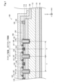
図1は、第1実施形態における半導体装置100の構成を模式的に示す断面図である。本実施形態では、半導体装置100は、縦型トレンチMOSFET(Metal-Oxide-Semiconductor Field-Effect Transistor)である。本実施形態では、半導体装置100は、電力制御に用いられ、パワーデバイスとも呼ばれる。
A. First Embodiment A-1. Configuration of Semiconductor Device FIG. 1 is a cross-sectional view schematically showing the configuration of the
図1には、相互に直交するXYZ軸が図示されている。図1のXYZ軸のうち、X軸は、図1の紙面左から紙面右に向かう軸である。+X軸方向は、紙面右に向かう方向であり、−X軸方向は、紙面左に向かう方向である。図1のXYZ軸のうち、Y軸は、図1の紙面手前から紙面奥に向かう軸である。+Y軸方向は、紙面奥に向かう方向であり、−Y軸方向は、紙面手前に向かう方向である。図1のXYZ軸のうち、Z軸は、図1の紙面下から紙面上に向かう軸である。+Z軸方向は、紙面上に向かう方向であり、−Z軸方向は、紙面下に向かう方向である。 FIG. 1 shows XYZ axes that are orthogonal to each other. Of the XYZ axes in FIG. 1, the X axis is an axis from the left side of the paper surface to the right side of the paper surface in FIG. The + X-axis direction is the direction toward the right side of the paper surface, and the −X-axis direction is the direction toward the left side of the paper surface. Of the XYZ axes of FIG. 1, the Y axis is an axis from the front side of the paper surface to the back side of the paper surface of FIG. The + Y-axis direction is the direction toward the back of the paper, and the −Y-axis direction is the direction toward the front of the paper. Of the XYZ axes of FIG. 1, the Z axis is an axis extending from below the paper surface to above the paper surface of FIG. The + Z-axis direction is the direction toward the top of the paper, and the −Z-axis direction is the direction toward the bottom of the paper.
半導体装置100は、基板110と、第1の半導体層112と、第2の半導体層114と、第3の半導体層116と、を備える。また、半導体装置100は、さらに、第1の絶縁膜130と、第2の絶縁膜132と、第3の絶縁膜150と、ソース電極141と、ボディ電極144と、ゲート電極142と、ドレイン電極143と、導電体146と、外周電極148と、配線電極160と、を備える。ここで、「ゲート電極142」が、「課題を解決するための手段」における「制御電極」に相当し、「ソース電極141」と「ボディ電極144」とが、「課題を解決するための手段」における「コンタクト電極」に相当する。
The
本実施形態では、基板110、第1の半導体層112、第2の半導体層114、及び第3の半導体層116は、ワイドバンドギャップ半導体により形成されている。ワイドバンドギャップ半導体としては、例えば、窒化ガリウム(GaN)、ダイヤモンド(C)、炭化ケイ素(SiC)、酸化ガリウム(GaO)が挙げられる。本実施形態では、基板110、第1の半導体層112、第2の半導体層114、及び第3の半導体層116は、窒化ガリウム(GaN)により形成されている。
In the present embodiment, the
基板110、第1の半導体層112、及び第3の半導体層116は、n型およびp型のうちの一方である第1導電型を有し、第2の半導体層114は、n型およびp型のうち第1導電型とは異なる第2導電型を有する。本実施形態では、基板110、第1の半導体層112、及び第3の半導体層116は、n型の特性を有し、第2の半導体層114は、p型の特性を有する。なお、基板110、第1の半導体層112、及び第3の半導体層116は、p型の特性を有し、第2の半導体層114は、n型の特性を有してもよい。
The
半導体装置100の基板110及び第1の半導体層112は、X軸及びY軸に沿って面方向に広がる板状の半導体層である。本実施形態では、基板110及び第1の半導体層112は、ケイ素(Si)をドナー元素として含有するn型半導体である。本実施形態では、基板110は、第1の半導体層112よりも高濃度のドナー元素を含有する。本実施形態では、第1の半導体層112は、有機金属気相成長法(MOCVD:Metal Organic Chemical Vapor Deposition)によって基板110の上に形成された層である。
The
半導体装置100の第2の半導体層114は、第1の半導体層112の上(+Z軸方向側)に位置し、X軸およびY軸に沿って広がる半導体層である。本実施形態では、第2の半導体層114は、マグネシウム(Mg)をアクセプタ元素として含有するp型半導体である。
The
半導体装置100の第3の半導体層116は、第2の半導体層114の上(+Z軸方向側)に位置し、X軸およびY軸に沿って広がる半導体層である。本実施形態では、第3の半導体層116は、ケイ素(Si)をドナー元素として含有するn型半導体である。
The
半導体装置100のコンタクト電極としてのボディ電極144は、第3の半導体層116を貫通するコンタクトホール124に形成された電極である。ボディ電極144は、第2の半導体層114と接する。本実施形態では、ボディ電極144は、第2の半導体層114とオーミック接触する。
The
本実施形態では、ボディ電極144は、パラジウム(Pd)から形成されている。なお、ボディ電極144を構成する材料は、これに限定されない。ボディ電極144は、例えば、(i)ニッケル(Ni)などのパラジウム以外の材料から形成されていてもよく、(ii)第2の半導体層114と接する層から順に、チタン(Ti)から形成されている層と、アルミニウム(Al)から形成されている層と、を備えていてもよい。ボディ電極144は、単層であってもよく、2層以上であってもよい。
In this embodiment, the
半導体装置100のコンタクト電極としてのソース電極141は、第3の半導体層116の上(+Z軸方向側)に形成された電極である。ソース電極141は、第3の半導体層116と接する。本実施形態では、ソース電極141は、第3の半導体層116とオーミック接触する。
The source electrode 141 as the contact electrode of the
本実施形態では、ソース電極141は、第3の半導体層116と接する層から順に、チタン(Ti)から形成されている層と、アルミニウム(Al)から形成されている層と、を備える。なお、ソース電極141を構成する材料は、これに限定されない。ソース電極141は、例えば、第3の半導体層116と接する層から順に、チタン(Ti)から形成されている層と、アルミニウム(Al)から形成されている層と、ニッケル(Ni)から形成されている層と、金(Au)から形成されている層と、を備えていてもよい。また、ソース電極141は、単層であってもよいし、2層以上であってもよい。ソース電極141は、ボディ電極144と接触していてもよく、第3の半導体層116及び第2の半導体層114と接し、ソース電極141とボディ電極144としての2つの機能を有する一つの電極であってもよい。
In the present embodiment, the
半導体装置100のトレンチ122は、第2の半導体層114と第3の半導体層116とを貫通し、第1の半導体層112まで到達している溝部である。本実施形態では、トレンチ122は、第1の半導体層112,第2の半導体層114,第3の半導体層116に対するドライエッチングによって形成される。
The
半導体装置100の第1の絶縁膜130は、トレンチ122の表面を覆い、電気絶縁性を有する膜である。本実施形態では、第1の絶縁膜130は、トレンチ122の内側に加え、第3の半導体層116における+Z軸方向側の面の一部にわたって形成されている。
The first insulating film 130 of the
本実施形態では、第1の絶縁膜130は、二酸化ケイ素(SiO2)から形成されている。第1の絶縁膜130を構成する材料は、電気絶縁性を有する材料であればよく、二酸化ケイ素(SiO2)の他、窒化ケイ素(SiNx)、酸化アルミニウム(Al2O3)、窒化アルミニウム(AlN)、酸化ジルコニウム(ZrO2)、酸化ハフニウム(HfO2)、酸窒化ケイ素(SiON)、酸窒化アルミニウム(AlON)、酸窒化ジルコニウム(ZrON)、酸窒化ハフニウム(HfON)などの少なくとも1つであってもよい。また、第1の絶縁膜130は、単層であってもよいし、2層以上であってもよい。 In the present embodiment, the first insulating film 130 is formed of silicon dioxide (SiO 2 ). The material constituting the first insulating film 130 may be any material having electrical insulating properties, and in addition to silicon dioxide (SiO 2 ), silicon nitride (SiNx), aluminum oxide (Al 2 O 3 ), and aluminum nitride (Al 2 O 3 ) AlN), zirconium oxide (ZrO 2 ), hafnium oxide (HfO 2 ), silicon nitride (SiON), aluminum nitride (AlON), zirconium oxynitride (ZrON), hafnium oxynitride (HfON), etc. There may be. Further, the first insulating film 130 may be a single layer or two or more layers.
半導体装置100の制御電極としてのゲート電極142は、第1の絶縁膜130に覆われたトレンチ122に形成された電極である。ゲート電極142に電圧が印加された場合、第2の半導体層114に反転層が形成され、この反転層がチャネルとして機能することによって、ソース電極141とドレイン電極143との間に導通経路が形成される。
The
本実施形態では、ゲート電極142は、アルミニウム(Al)から形成されている。なお、ゲート電極142を構成する材料として、他の材料を用いてもよい。例えば、ゲート電極142は、チタン(Ti)から形成されていてもよく、ポリシリコンや、金属窒化物により形成されていてもよい。ゲート電極142は、単層であってもよいし、2層以上であってもよい。なお、図1には図示されていないが、例えば、図2に図示されているように、ゲート電極142同士は、互いに電気的に接続されている。
In this embodiment, the
半導体装置100は、アクティブ領域と、アクティブ領域の外周を囲む非アクティブ領域とを備える。アクティブ領域とは、半導体装置100を駆動する際に主として電流が流れる領域をいう。外周トレンチ129と外周トレンチ129に隣接するトレンチ122との間に設けられたボディ電極144を境界にして、内周側がアクティブ領域であり、外周側が非アクティブ領域である。半導体装置100は、アクティブ領域において、トレンチ122と、第1の絶縁膜130と、ゲート電極142と、ソース電極141とを備え、非アクティブ領域において、外周トレンチ129と、第2の絶縁膜132と、導電体146と、外周電極148とを備える。
The
半導体装置100の外周トレンチ129は、アクティブ領域を囲み、ゲート電極142及びソース電極141の外周側に位置する溝部である。外周トレンチ129は、第3の半導体層116と第2の半導体層114とを貫通し、第1の半導体層112まで到達している溝部である。本実施形態では、外周トレンチ129は、トレンチ122と同じ深さである。このようにすることにより、トレンチ122を形成するエッチング工程において、外周トレンチ129を同時に作成することができる。なお、外周トレンチ129の深さは、トレンチ122の深さと異なっていてもよい。
The outer
本実施形態において、隣接するトレンチ122間の距離aは、外周トレンチ129と外周トレンチ129に隣接するトレンチ122との距離bと等しい。ここで、隣接するトレンチ122間の距離aは、複数のボディ電極144の中心軸を通る面において、隣接するトレンチ122の中心軸間の距離を言う。同様に、外周トレンチ129と外周トレンチ129に隣接するトレンチ122との距離bは、複数のボディ電極144の中心軸を通る面において、隣接するトレンチ122の中心軸から外周トレンチ129の中心軸までの距離を言う。ここで、図1に示す断面は、複数のボディ電極144の中心軸を通る面である。
In the present embodiment, the distance a between the
半導体装置100の第2の絶縁膜132は、外周トレンチ129の表面を覆い、電気絶縁性を有する膜である。本実施形態では、第2の絶縁膜132は、外周トレンチ129の内側に加え、第3の半導体層116における+Z軸方向側の面の一部にわたって形成されている。
The second
本実施形態では、第2の絶縁膜132は、酸化アルミニウム(Al2O3)から形成されている。このため、本実施形態では、第2の絶縁膜132の誘電率は、第1の絶縁膜130の誘電率よりも大きい。このようにすることにより、最外周に位置するトレンチ122の外周側の底面付近における電界集中を、より効果的に緩和できる。第1の絶縁膜130よりも誘電率の大きい材料として、例えば、窒化アルミニウム(AlN)、酸化ジルコニウム(ZrO2)、酸化ハフニウム(HfO2)、酸窒化ケイ素(SiON)、酸窒化アルミニウム(AlON)、酸窒化ジルコニウム(ZrON)、酸窒化ハフニウム(HfON)などを用いてもよい。なお、第2の絶縁膜132の材料として、第1の絶縁膜130と同じ材料を用いてもよい。このようにすることにより、第2の絶縁膜132を第1の絶縁膜130の作成時と同時に形成することができる。
In the present embodiment, the second
半導体装置100の導電体146は、第2の絶縁膜132に覆われた外周トレンチ129に形成された層である。導電体146は、ゲート電極142及びソース電極141と電気的に絶縁されている。つまり、導電体146は、電気的に浮遊状態となっている。本実施形態では、導電体146は、アルミニウム(Al)から形成されている。なお、導電体146を構成する材料として、他の材料を用いてもよい。例えば、導電体146は、チタン(Ti)等の他の金属から形成されていてもよく、ポリシリコンや、金属窒化物等の他の導電材料により形成されていてもよい。
The
半導体装置100の外周電極148は、第3の半導体層116を貫通するコンタクトホール126に形成された電極である。外周電極148は、外周トレンチ129の外側に位置し、かつ、第2の半導体層114と接する。本実施形態では、外周電極148は、外周トレンチ129の外周を囲む。外周電極148は、ソース電極141と配線電極160を介して電気的に接続されている。本実施形態では、外周電極148は、パラジウム(Pd)から形成されている。なお、外周電極148を構成する材料は、これに限定されない。外周電極148は、例えば、(i)ニッケル(Ni)等の他の金属から形成されていてもよく、(ii)第2の半導体層114と接する層から順に、チタン(Ti)から形成されている層と、アルミニウム(Al)から形成されている層と、を備えていてもよい。外周電極148は、単層から構成されていてもよく、複数の層から構成されていてもよい。また、外周電極148は、第2の半導体層114とオーミック接触する。
The outer
半導体装置100のトレンチ128は、半導体層114,116の厚さ方向(−Z軸方向)を深さ方向とする溝部である。トレンチ128は、第3の半導体層116と第2の半導体層114とを貫通し、第1の半導体層112まで到達している溝部である。本実施形態では、トレンチ128は、トレンチ122や外周トレンチ129よりも深い。トレンチ128は、半導体装置100を他の素子から分離するために用いる。本実施形態では、トレンチ128は、外周電極148よりもさらに外周側に位置する。
The
半導体装置100の第3の絶縁膜150は、半導体層112、114、116の表面(+Z軸方向側の面)を覆うように形成されている。第3の絶縁膜150は、ソース電極141、ボディ電極144、及びゲート電極142の一部が露出するように開口部が形成されている。本実施形態では、第3の絶縁膜150は、酸化アルミニウム(Al2O3)から形成されている。第3の絶縁膜150の材質は、電気絶縁性を有する材質であればよく、酸化アルミニウム(Al2O3)の他、二酸化ケイ素(SiO2)、窒化ケイ素(SiNx)、窒化アルミニウム(AlN)、酸化ジルコニウム(ZrO2)、酸化ハフニウム(HfO2)、酸窒化ケイ素(SiON)、酸窒化アルミニウム(AlON)、酸窒化ジルコニウム(ZrON)、酸窒化ハフニウム(HfON)などの少なくとも1つであってもよい。第3の絶縁膜150は、単層から構成されていてもよく、複数の層から構成されていてもよい。
The third
配線電極160は、第3の絶縁膜150の上(+Z軸方向側)に形成された電極である。配線電極160により、ソース電極141、ボディ電極144、外周電極148が電気的に接続されている。配線電極160は、第3の絶縁膜150に覆われたトレンチ128の側壁及び底面においても形成されている。
The
半導体装置100のドレイン電極143は、基板110の−Z軸方向側の面に形成された電極である。ドレイン電極143は、基板110と接する。本実施形態では、ドレイン電極143は、基板110とオーミック接触する。
The
本実施形態では、ドレイン電極143は、基板110と接する層から順に、チタン(Ti)から形成されている層と、アルミニウム(Al)から形成されている層と、を備える。なお、ドレイン電極143を構成する材料として、他の材料を用いてもよい。例えば、ドレイン電極143は、基板110と接する層から順に、チタン(Ti)から形成されている層と、アルミニウム(Al)から形成されている層と、ニッケル(Ni)から形成されている層と、金(Au)から形成されている層と、を備えていてもよい。ドレイン電極143は、単層から構成されていてもよく、複数の層から構成されていてもよい。
In the present embodiment, the
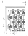
図2は、図1を+Z軸方向から見た模式図である。つまり、図2は、面方向(X軸方向およびY軸方向)に直交する厚み方向(Z軸方向)から見た平面図である。図2では、理解を容易にする観点から、第1の絶縁膜130、第2の絶縁膜132、第3の絶縁膜150及び配線電極160の記載が省略されている。図2におけるI−I断面が図1に相当する。
FIG. 2 is a schematic view of FIG. 1 as viewed from the + Z axis direction. That is, FIG. 2 is a plan view seen from the thickness direction (Z-axis direction) orthogonal to the plane direction (X-axis direction and Y-axis direction). In FIG. 2, from the viewpoint of facilitating understanding, the description of the first insulating film 130, the second
図2に示されるように、本実施形態では、ボディ電極144は、六角形状となっている。ソース電極141は、第3の半導体層116を介してボディ電極144を囲んでおり、ソース電極141の内周および外周は、いずれも六角形状となっている。本実施形態では、半導体装置100は、複数のボディ電極144と複数のソース電極141とを備える。ソース電極141として、ゲート電極142よりも外周側に配置され、かつ、導電体146よりも内周側に配置されているソース電極141についても存在する。
As shown in FIG. 2, in the present embodiment, the
本実施形態では、ゲート電極142は、第3の半導体層116を介してソース電極141を囲んでいる。ゲート電極142は、半導体装置100の表面(+Z軸方向側の面)上でつながっており、六角形を隙間無く並べた網目状の形状となっている。
In this embodiment, the
外周トレンチ129は、ゲート電極142及びソース電極141の外周側を途切れることなく連続的に囲んでもいるが、部分的に非連続となっていてもよい。本実施形態では、外周トレンチ129は、ゲート電極142及びソース電極141の外周側を一重に囲んでいるが、多重に囲んでいてもよい。なお、本実施形態のように一重とすることにより、非アクティブ領域の面積を少なくすることができる結果、アクティブ領域を相対的に広くすることができる。
The outer
A−2.効果
以上説明したように、本実施形態の半導体装置100によれば、導電体146に加えて外周電極148を備えるため、アクティブ領域の最外周に位置する外周トレンチ129の底面端部近傍の電界集中を緩和できる。以下、半導体装置100により得られる効果について説明する。
A-2. Effect As described above, according to the
図3は、最も電界集中が起こりやすいトレンチ底面端部における電界強度比を示す図である。ここで、電界強度が高いほど、電界集中が起こりやすく、一般に、最外周のトレンチ122の底面端部は、それ以外のトレンチ122の底面端部と比較して、電界集中が起こりやすい。
FIG. 3 is a diagram showing an electric field strength ratio at the bottom end of the trench where electric field concentration is most likely to occur. Here, the higher the electric field strength, the more likely it is that electric field concentration will occur, and in general, the bottom end of the
図3の縦軸として、最外周ではないトレンチ122の底面端部における電界強度を1とした場合の電界強度比を示す。図3では、(i)最外周ではないトレンチ122の底面端部における電界強度比と、(ii)最外周のトレンチ122の底面端部における電界強度比と、(iii)外周トレンチ129の底面端部における電界強度比と、を示す。
The vertical axis of FIG. 3 shows the electric field strength ratio when the electric field strength at the bottom end of the
図3において、(i)外周トレンチ129を備えない場合と、(ii)第2の絶縁膜132に覆われた外周トレンチ129に導電体146を備えるが、導電体146が他の電極と接続されている場合と、(iii)第2の絶縁膜132に覆われた外周トレンチ129に導電体146を備え、導電体146は他の電極と接続されていない場合と、(iv)外周トレンチ129の内部に絶縁膜のみが設けられている場合と、を示す。
In FIG. 3, (i) the case where the outer
図3の結果から、以下のことが分かる。外周トレンチ129の内部に絶縁膜のみが設けられている場合、及び、外周トレンチ129を備えない場合、最外周のトレンチ122の底面端部における電界強度比が大きくなるため、好ましくない。また、外周トレンチ129に導電体146を備えるが、他の電極と接続されている場合、外周トレンチ129の底面端部における電界強度比が高くなるため、好ましくない。
From the results of FIG. 3, the following can be seen. When only the insulating film is provided inside the outer
一方、第2の絶縁膜132に覆われた外周トレンチ129に導電体146を備え、導電体146は他の電極と接続されていない場合、最外周ではないトレンチ122の底面端部における電界強度比と、最外周のトレンチ122の底面端部における電界強度比とが同等である。また、この場合、外周トレンチ129の底面端部における電界強度比は、最外周のトレンチ122の底面端部における電界強度比よりも低い。このため、この場合が図3の条件の中で一番好ましいことが分かる。
On the other hand, when the outer
図4は、トレンチ122の表面を覆う第1の絶縁膜130と、外周トレンチ129の表面を覆う第2の絶縁膜132との誘電率の関係を示す図である。図4の縦軸として、図3と同様に、最外周ではないトレンチ122の底面端部における電界強度を1とした場合の電界強度比を示す。図4での電界強度とは、絶縁膜中における最大電界強度を示す。また、図4においても、図3と同様に、(i)最外周ではないトレンチ122の底面端部における電界強度比と、(ii)最外周のトレンチ122の底面端部における電界強度比と、(iii)外周トレンチ129の底面端部における電界強度比と、を示す。
FIG. 4 is a diagram showing the relationship between the dielectric constants of the first insulating film 130 covering the surface of the
図4において、(i)第2の絶縁膜132の誘電率が、第1の絶縁膜130の誘電率よりも大きい場合と、(ii)第2の絶縁膜132の誘電率が、第1の絶縁膜130の誘電率と同じ場合と、(iii)第2の絶縁膜132の誘電率が、第1の絶縁膜130の誘電率よりも小さい場合と、を示す。
In FIG. 4, (i) the case where the dielectric constant of the second
図4の結果から、以下のことが分かる。第2の絶縁膜132の誘電率が、第1の絶縁膜130の誘電率よりも小さい場合、最外周のトレンチ122の底面端部における電界強度比は、最外周ではないトレンチ122の底面端部における電界強度比よりも大きい。さらに、外周トレンチ129の底面端部における電界強度比は、最外周のトレンチ122の底面端部における電界強度比よりも大きい。このため、最外周のトレンチ122の底面端部及び外周トレンチ129の底面端部において、電界集中が発生しているため好ましくない。
From the results of FIG. 4, the following can be seen. When the dielectric constant of the second
一方、本実施形態の構成である場合、つまり、第2の絶縁膜132の誘電率が、第1の絶縁膜130の誘電率よりも大きい場合、最外周ではないトレンチ122の底面端部における電界強度比よりも、最外周のトレンチ122の底面端部における電界強度比のほうが小さい。さらに、外周トレンチ129の底面端部における電界強度比は、最外周のトレンチ122の底面端部における電界強度比よりも小さい。このため、最外周のトレンチ122の底面端部及び外周トレンチ129の底面端部において、電界集中が緩和されていることが分かる。
On the other hand, in the case of the configuration of the present embodiment, that is, when the dielectric constant of the second
図5から図7は、電界強度分布のシミュレーション結果を示す図である。図5は、本実施形態と同様に、導電体146と外周電極148を備える構造のシミュレーション結果を示す。図6は、本実施形態から外周電極148を除外した構造のシミュレーション結果を示す。図7は、本実施形態から外周電極148を除外し、導電体146を二重に備える構造のシミュレーション結果を示す。図5から図7において、第1の半導体層112内の太線は、図5から図7のいずれも同電位の等電位線を示す。
5 to 7 are diagrams showing simulation results of the electric field strength distribution. FIG. 5 shows a simulation result of a structure including a
図6の場合、つまり、本実施形態から外周電極148を除外した構造の場合、電位がX軸方向に広がらず、図6の領域T1に示すように、外周トレンチ129の底面端部の近傍において電界が集中していることが分かる。同様に、図7の場合、つまり、及び本実施形態から外周電極148を除外し、導電体146を二重に備える構造の場合においても、図7の領域T2に示すように、外周トレンチ129の底面端部の近傍において電界が集中していることが分かる。一方、本実施形態のシミュレーション結果を示す図5では、電位がX軸方向に広がっているため、外周トレンチ129の底面端部の近傍への電界集中が緩和していることが分かる。つまり、本実施形態の半導体装置100によれば、導電体146に加えて外周電極148を備えるため、外周トレンチ129の底面端部近傍の電界集中を緩和できる。
In the case of FIG. 6, that is, in the case of the structure excluding the outer
B.第2実施形態
図8は、第2実施形態における半導体装置100bの構成を模式的に示す断面図である。図8及びそれ以降の図では、理解を容易にする観点から、第1の絶縁膜130、第2の絶縁膜132、第3の絶縁膜150及び配線電極160の記載が省略されている。半導体装置100bは、第1実施形態における半導体装置100と比較して、最外周のトレンチ122とゲート電極142の形状が異なる。
B. Second Embodiment FIG. 8 is a cross-sectional view schematically showing the configuration of the
第2実施形態では、厚み方向(Z軸方向)から見たとき、ゲート電極142は、ゲート電極142の角のうち、最も導電体146に近い角において、導電体146に向かって突出する突出部142bを備える。第2実施形態の半導体装置100bによれば、突出部142bを備えるため、1チップあたりのゲート幅を増やすことができるため、大きな電流を流すことができる。
In the second embodiment, when viewed from the thickness direction (Z-axis direction), the
C.第3実施形態
図9は、第3実施形態における半導体装置100cの構成を模式的に示す断面図である。半導体装置100cは、第1実施形態における半導体装置100と比較して、導電体146の形状が異なる。
C. Third Embodiment FIG. 9 is a cross-sectional view schematically showing the configuration of the
第3実施形態では、厚み方向(Z軸方向)から見たとき、導電体146は、導電体146の角のうち、最もゲート電極142に近い角において、ゲート電極142に向かって突出する突出部146cを備える。第3実施形態の半導体装置100cによれば、突出部146cを備えるため、ゲート電極142の最も導電体146に近い角におけるトレンチ122底面付近の電界集中をより効果的に緩和できる。
In the third embodiment, when viewed from the thickness direction (Z-axis direction), the
D.第4実施形態
図10は、第4実施形態における半導体装置100dの構成を模式的に示す断面図である。半導体装置100dは、第1実施形態における半導体装置100と比較して、最も外周側のソース電極141の形状が異なる。
D. Fourth Embodiment FIG. 10 is a cross-sectional view schematically showing the configuration of the semiconductor device 100d according to the fourth embodiment. The shape of the
第4実施形態では、最も外周側に配置された複数のソース電極141において、隣接するソース電極141を電気的に接続する接続部141dを備える。第4実施形態の半導体装置100dによれば、接続部141dを備えるため、接続部141dにおいても電流が流れるため、大きな電流を流すことができる。
In the fourth embodiment, the plurality of
E.第5実施形態
図11は、第5実施形態における半導体装置100eの構成を模式的に示す断面図である。半導体装置100eは、第1実施形態における半導体装置100と比較して、トレンチ122の外周の形状と、最も外周側のソース電極141e及び最も外周側のボディ電極144eの形状とが異なる。
E. Fifth Embodiment FIG. 11 is a cross-sectional view schematically showing the configuration of the
第5実施形態では、厚み方向(Z軸方向)から見たとき、トレンチ122の最も外周側の端部は、外周トレンチ129までの距離が一定となるように形成されている。このため、本実施形態では、トレンチ122の最も外周側の端部と、外周トレンチ129とが平行となっている。
In the fifth embodiment, when viewed from the thickness direction (Z-axis direction), the outermost end of the
また、トレンチ122の最も外周側の端部と、最も外周側のソース電極141eとの距離が一定となるように形成されている。同様に、トレンチ122の最も外周側の端部と、最も外周側のボディ電極144eとの距離が一定となるように形成されている。本実施形態では、トレンチ122の最も外周側の端部と、最も外周側のソース電極141eと、最も外周側のボディ電極144eと、が平行となっている。
Further, the
第5実施形態の半導体装置100eによれば、トレンチ122の最も外周側の端部は、外周トレンチ129までの距離が一定となるように形成されているため、トレンチ122の最も外周側の端部底面付近における電界集中を、より効果的に緩和できる。
According to the
F.他の実施形態
本発明は、上述の実施形態や実施例に限られるものではなく、その趣旨を逸脱しない範囲において種々の構成で実現することができる。例えば、発明の概要の欄に記載した各形態中の技術的特徴に対応する実施形態、実施例、変形例中の技術的特徴は、上述の課題の一部または全部を解決するために、あるいは、上述の効果の一部または全部を達成するために、適宜、差し替えや、組み合わせを行うことが可能である。また、その技術的特徴が本明細書中に必須なものとして説明されていなければ、適宜、削除することが可能である。
F. Other Embodiments The present invention is not limited to the above-described embodiments and examples, and can be realized with various configurations within a range not deviating from the gist thereof. For example, the technical features in the embodiments, examples, and modifications corresponding to the technical features in each embodiment described in the column of the outline of the invention may be used to solve some or all of the above-mentioned problems. , It is possible to replace or combine as appropriate in order to achieve some or all of the above effects. Further, if the technical feature is not described as essential in the present specification, it can be appropriately deleted.
本発明が適用される半導体装置は、上述の実施形態で説明した縦型トレンチMOSFETに限られず、例えば、絶縁ゲートバイポーラトランジスタ(IGBT)などのトレンチゲート構造を備える装置に適用できる。 The semiconductor device to which the present invention is applied is not limited to the vertical trench MOSFET described in the above-described embodiment, and can be applied to a device having a trench gate structure such as an insulated gate bipolar transistor (IGBT).
上述の実施形態において、第2の半導体層114に含まれるアクセプタ元素は、マグネシウム(Mg)であるが、例えば、亜鉛(Zn)を用いてもよい。
In the above-described embodiment, the acceptor element contained in the
上述の実施形態において、基板110、第1の半導体層112、及び第3の半導体層116に含まれるドナー元素は、ケイ素(Si)であるが、例えば、ゲルマニウム(Ge)を用いてもよい。
In the above-described embodiment, the donor element contained in the
上述の実施形態において、厚み方向からみたとき、ゲート電極142は、六角形を隙間無く並べた網目状の形状となっており、導電体146は、六角形を隙間無く並べた形状の外周に沿った形状となっている。しかし、六角形に限らず、例えば、三角形や四角形などの多角形でもよく、最密配列であることが好ましい。
In the above-described embodiment, when viewed from the thickness direction, the
第2実施形態から第4実施形態の各特徴は、任意に組み合わせてもよい。 The features of the second to fourth embodiments may be arbitrarily combined.
100…半導体装置
100b…半導体装置
100c…半導体装置
100d…半導体装置
100e…半導体装置
110…基板
112…第1の半導体層
114…第2の半導体層
116…第3の半導体層
122…トレンチ
124…コンタクトホール
126…コンタクトホール
128…トレンチ
129…外周トレンチ
130…第1の絶縁膜
132…第2の絶縁膜
141…ソース電極
141d…接続部
141e…ソース電極
142…ゲート電極
142b…突出部
143…ドレイン電極
144…ボディ電極
144e…ボディ電極
146…導電体
146c…突出部
148…外周電極
150…第3の絶縁膜
160…配線電極
T1…領域
T2…領域
a…距離
b…距離
100 ...
Claims (6)
第1導電型を有し、面方向に広がる第1の半導体層と、
前記第1の半導体層の上に形成され、前記第1導電型とは異なる第2導電型を有する第2の半導体層と、
前記第2の半導体層の上に形成され、前記第1導電型を有する第3の半導体層と、を備え、
前記第1の半導体層と、前記第2の半導体層と、前記第3の半導体層とは、ワイドバンドギャップ半導体により形成されており、
前記アクティブ領域は、
前記第3の半導体層と前記第2の半導体層とを貫通し、前記第1の半導体層まで到達したトレンチと、
前記トレンチの表面を覆う第1の絶縁膜と、
前記第1の絶縁膜に覆われた前記トレンチに形成された制御電極と、
前記第3の半導体層と接するコンタクト電極と、を備え、
前記非アクティブ領域は、
前記第3の半導体層と前記第2の半導体層とを貫通し、前記第1の半導体層まで到達しており、前記アクティブ領域を囲む外周トレンチと、
前記外周トレンチの表面を覆う第2の絶縁膜と、
前記第2の絶縁膜に覆われた前記外周トレンチに形成され、前記制御電極及び前記コンタクト電極と電気的に絶縁された導電体と、
前記外周トレンチの外側に位置し、前記第2の半導体層と接し、前記コンタクト電極と電気的に接続された外周電極と、を備える、半導体装置。 A semiconductor device including an active region and an inactive region surrounding the outer periphery of the active region.
A first semiconductor layer having a first conductive type and spreading in the plane direction,
A second semiconductor layer formed on the first semiconductor layer and having a second conductive type different from the first conductive type,
A third semiconductor layer formed on the second semiconductor layer and having the first conductive type is provided.
The first semiconductor layer, the second semiconductor layer, and the third semiconductor layer are formed of a wide bandgap semiconductor.
The active area is
A trench that penetrates the third semiconductor layer and the second semiconductor layer and reaches the first semiconductor layer,
A first insulating film covering the surface of the trench and
A control electrode formed in the trench covered with the first insulating film and
A contact electrode in contact with the third semiconductor layer is provided.
The inactive area is
An outer peripheral trench that penetrates the third semiconductor layer and the second semiconductor layer, reaches the first semiconductor layer, and surrounds the active region.
A second insulating film covering the surface of the outer trench and
A conductor formed in the outer peripheral trench covered with the second insulating film and electrically insulated from the control electrode and the contact electrode,
A semiconductor device including an outer peripheral electrode located outside the outer peripheral trench, in contact with the second semiconductor layer, and electrically connected to the contact electrode.
前記第2の絶縁膜の誘電率は、前記第1の絶縁膜の誘電率よりも大きい、半導体装置。 The semiconductor device according to claim 1.
A semiconductor device in which the dielectric constant of the second insulating film is larger than the dielectric constant of the first insulating film.
前記面方向に直交する厚み方向から見たとき、
前記制御電極は、多角形を隙間無く並べた網目状の形状となっており、前記多角形の角のうち、最も前記導電体に近い角において、前記導電体に向かって突出する突出部を備える、半導体装置。 The semiconductor device according to claim 1 or 2.
When viewed from the thickness direction orthogonal to the plane direction,
The control electrode has a mesh-like shape in which polygons are arranged without gaps, and includes a projecting portion that projects toward the conductor at an angle closest to the conductor among the corners of the polygon. , Semiconductor device.
前記面方向に直交する厚み方向から見たとき、
前記制御電極は、多角形を隙間無く並べた網目状の形状となっており、
前記導電体は、前記多角形を隙間無く並べた形状の外周に沿った形状となっており、
前記導電体は、前記導電体の前記多角形の角のうち、最も前記制御電極に近い角において、前記制御電極に向かって突出する突出部を備える、半導体装置。 The semiconductor device according to any one of claims 1 to 3.
When viewed from the thickness direction orthogonal to the plane direction,
The control electrode has a mesh-like shape in which polygons are arranged without gaps.
The conductor has a shape along the outer circumference of the shape in which the polygons are arranged without gaps.
The conductor is a semiconductor device including a protruding portion that projects toward the control electrode at an angle closest to the control electrode among the polygonal corners of the conductor.
前記コンタクト電極を複数備え、
前記制御電極よりも外周側に配置され、前記導電体よりも内側に配置された複数の前記コンタクト電極において、隣接する前記コンタクト電極を電気的に接続する接続部を備える、半導体装置。 The semiconductor device according to any one of claims 1 to 4.
A plurality of the contact electrodes are provided.
A semiconductor device comprising a connection portion for electrically connecting adjacent contact electrodes in a plurality of contact electrodes arranged on the outer peripheral side of the control electrode and arranged inside the conductor.
前記トレンチの最も外周側の端部は、前記外周トレンチまでの距離が一定となるように形成されている、半導体装置。 The semiconductor device according to claim 1 or 2.
A semiconductor device in which the outermost end of the trench is formed so that the distance to the outer peripheral trench is constant.
Priority Applications (3)
| Application Number | Priority Date | Filing Date | Title |
|---|---|---|---|
| JP2017187744A JP6791084B2 (en) | 2017-09-28 | 2017-09-28 | Semiconductor device |
| US16/129,554 US10403727B2 (en) | 2017-09-28 | 2018-09-12 | Semiconductor device |
| CN201811107461.3A CN109585537B (en) | 2017-09-28 | 2018-09-21 | Semiconductor device with a plurality of semiconductor chips |
Applications Claiming Priority (1)
| Application Number | Priority Date | Filing Date | Title |
|---|---|---|---|
| JP2017187744A JP6791084B2 (en) | 2017-09-28 | 2017-09-28 | Semiconductor device |
Publications (3)
| Publication Number | Publication Date |
|---|---|
| JP2019062160A JP2019062160A (en) | 2019-04-18 |
| JP2019062160A5 JP2019062160A5 (en) | 2020-02-06 |
| JP6791084B2 true JP6791084B2 (en) | 2020-11-25 |
Family
ID=65807896
Family Applications (1)
| Application Number | Title | Priority Date | Filing Date |
|---|---|---|---|
| JP2017187744A Active JP6791084B2 (en) | 2017-09-28 | 2017-09-28 | Semiconductor device |
Country Status (3)
| Country | Link |
|---|---|
| US (1) | US10403727B2 (en) |
| JP (1) | JP6791084B2 (en) |
| CN (1) | CN109585537B (en) |
Families Citing this family (10)
| Publication number | Priority date | Publication date | Assignee | Title |
|---|---|---|---|---|
| JP2019165182A (en) * | 2018-03-20 | 2019-09-26 | 株式会社東芝 | Semiconductor device |
| JP6946219B2 (en) * | 2018-03-23 | 2021-10-06 | 株式会社東芝 | Semiconductor device |
| US10636902B2 (en) * | 2018-09-13 | 2020-04-28 | Ptek Technology Co., Ltd. | Multiple gated power MOSFET device |
| DE102019101304B4 (en) * | 2019-01-18 | 2023-04-27 | Infineon Technologies Dresden GmbH & Co. KG | Power semiconductor device and method of forming a power semiconductor device |
| JP7242489B2 (en) * | 2019-09-18 | 2023-03-20 | 株式会社東芝 | semiconductor equipment |
| JP7295052B2 (en) * | 2020-02-28 | 2023-06-20 | 株式会社東芝 | semiconductor equipment |
| JP7331783B2 (en) | 2020-05-29 | 2023-08-23 | 豊田合成株式会社 | Semiconductor device manufacturing method |
| JP7327283B2 (en) | 2020-05-29 | 2023-08-16 | 豊田合成株式会社 | semiconductor equipment |
| JP7347335B2 (en) | 2020-05-29 | 2023-09-20 | 豊田合成株式会社 | semiconductor equipment |
| EP3971987A1 (en) * | 2020-09-21 | 2022-03-23 | Infineon Technologies AG | Silicon carbide device with stripe-shaped gate electrode and source metallization |
Family Cites Families (14)
| Publication number | Priority date | Publication date | Assignee | Title |
|---|---|---|---|---|
| US6566691B1 (en) * | 1999-09-30 | 2003-05-20 | Kabushiki Kaisha Toshiba | Semiconductor device with trench gate having structure to promote conductivity modulation |
| JP2007123570A (en) | 2005-10-28 | 2007-05-17 | Toyota Industries Corp | Semiconductor device |
| JP2008108844A (en) * | 2006-10-24 | 2008-05-08 | Toyota Central R&D Labs Inc | Group iii nitride semiconductor device having trench or mesa-structure, and manufacturing method thereof |
| JP5315638B2 (en) | 2007-07-24 | 2013-10-16 | サンケン電気株式会社 | Semiconductor device |
| JP5609876B2 (en) * | 2009-08-28 | 2014-10-22 | サンケン電気株式会社 | Semiconductor device |
| US8564053B2 (en) * | 2009-11-20 | 2013-10-22 | Force Mos Technology Co., Ltd. | Trench MOSFET with trenched floating gates in termination |
| JP5556863B2 (en) * | 2012-08-10 | 2014-07-23 | 富士電機株式会社 | Wide bandgap semiconductor vertical MOSFET |
| JP6139356B2 (en) * | 2013-09-24 | 2017-05-31 | トヨタ自動車株式会社 | Semiconductor device |
| DE102014112371B4 (en) * | 2014-08-28 | 2023-11-23 | Infineon Technologies Austria Ag | SEMICONDUCTOR DEVICE AND ELECTRONIC ARRANGEMENT COMPRISING A SEMICONDUCTOR DEVICE |
| JP6341077B2 (en) * | 2014-12-09 | 2018-06-13 | 豊田合成株式会社 | Manufacturing method of semiconductor device |
| JP2016189369A (en) * | 2015-03-30 | 2016-11-04 | サンケン電気株式会社 | Semiconductor device |
| DE102016103384B4 (en) * | 2016-02-25 | 2024-02-08 | Infineon Technologies Austria Ag | Semiconductor device with needle-shaped field plate structures in a transistor cell region and in an inner termination region |
| CN106653824A (en) * | 2016-10-19 | 2017-05-10 | 珠海格力电器股份有限公司 | Trench type metal oxide semiconductor power device and manufacture method |
| CN106298544B (en) * | 2016-11-04 | 2023-06-06 | 无锡新洁能股份有限公司 | Method for manufacturing trench DMOS device and structure |
-
2017
- 2017-09-28 JP JP2017187744A patent/JP6791084B2/en active Active
-
2018
- 2018-09-12 US US16/129,554 patent/US10403727B2/en active Active
- 2018-09-21 CN CN201811107461.3A patent/CN109585537B/en active Active
Also Published As
| Publication number | Publication date |
|---|---|
| JP2019062160A (en) | 2019-04-18 |
| CN109585537B (en) | 2021-09-14 |
| CN109585537A (en) | 2019-04-05 |
| US10403727B2 (en) | 2019-09-03 |
| US20190097004A1 (en) | 2019-03-28 |
Similar Documents
| Publication | Publication Date | Title |
|---|---|---|
| JP6791084B2 (en) | Semiconductor device | |
| US10950524B2 (en) | Heterojunction semiconductor device for reducing parasitic capacitance | |
| US8541834B2 (en) | Semiconductor device and method for manufacturing same | |
| US20170200818A1 (en) | Semiconductor device | |
| JP6415749B2 (en) | Silicon carbide semiconductor device | |
| US10833185B2 (en) | Heterojunction semiconductor device having source and drain pads with improved current crowding | |
| JP2022191421A (en) | Semiconductor device | |
| JP2017045776A (en) | Semiconductor device and manufacturing method of the same | |
| JP2020136472A (en) | Semiconductor device | |
| JP7464763B2 (en) | Nitride Semiconductor Device | |
| US9035320B2 (en) | Semiconductor device | |
| JP5556863B2 (en) | Wide bandgap semiconductor vertical MOSFET | |
| JP6966844B2 (en) | Semiconductor device | |
| US11158713B2 (en) | Semiconductor device | |
| JP7343315B2 (en) | silicon carbide semiconductor device | |
| US20130221402A1 (en) | Insulated gate bipolar transistor | |
| US9236438B2 (en) | Semiconductor device | |
| JP6854598B2 (en) | Semiconductor device | |
| JP7188230B2 (en) | semiconductor equipment | |
| US20170243971A1 (en) | Semiconductor device | |
| JP2019040961A (en) | Nitride semiconductor device | |
| US10978586B2 (en) | Switching device | |
| KR102183362B1 (en) | Semiconductor device including Trench MOSFET having high breakdown voltage | |
| TWI660506B (en) | Semiconductor device | |
| CN112889158B (en) | Semiconductor device with a semiconductor device having a plurality of semiconductor chips |
Legal Events
| Date | Code | Title | Description |
|---|---|---|---|
| A621 | Written request for application examination |
Free format text: JAPANESE INTERMEDIATE CODE: A621 Effective date: 20191107 |
|
| A521 | Request for written amendment filed |
Free format text: JAPANESE INTERMEDIATE CODE: A523 Effective date: 20191217 |
|
| A977 | Report on retrieval |
Free format text: JAPANESE INTERMEDIATE CODE: A971007 Effective date: 20200831 |
|
| TRDD | Decision of grant or rejection written | ||
| A01 | Written decision to grant a patent or to grant a registration (utility model) |
Free format text: JAPANESE INTERMEDIATE CODE: A01 Effective date: 20201006 |
|
| A61 | First payment of annual fees (during grant procedure) |
Free format text: JAPANESE INTERMEDIATE CODE: A61 Effective date: 20201019 |
|
| R150 | Certificate of patent or registration of utility model |
Ref document number: 6791084 Country of ref document: JP Free format text: JAPANESE INTERMEDIATE CODE: R150 |