JP6944672B2 - Electromagnetic field sensor, electromagnetic field measurement system and electromagnetic wave arrival direction estimation system - Google Patents
Electromagnetic field sensor, electromagnetic field measurement system and electromagnetic wave arrival direction estimation system Download PDFInfo
- Publication number
- JP6944672B2 JP6944672B2 JP2016247023A JP2016247023A JP6944672B2 JP 6944672 B2 JP6944672 B2 JP 6944672B2 JP 2016247023 A JP2016247023 A JP 2016247023A JP 2016247023 A JP2016247023 A JP 2016247023A JP 6944672 B2 JP6944672 B2 JP 6944672B2
- Authority
- JP
- Japan
- Prior art keywords
- electromagnetic field
- resistor
- voltage
- electromagnetic
- field sensor
- Prior art date
- Legal status (The legal status is an assumption and is not a legal conclusion. Google has not performed a legal analysis and makes no representation as to the accuracy of the status listed.)
- Active
Links
Images


Description
本発明は、電磁界センサ、電磁界計測システムおよび電磁波の到来方向推定システムに関する。 The present invention relates to an electromagnetic field sensor, an electromagnetic field measurement system, and an electromagnetic wave arrival direction estimation system.
近年、電子機器の普及により電磁波環境は複雑化し、不要電磁波を低減させたり不要電磁波の発生源の位置を推定することにより、電磁干渉の原因を探索することが求められている。不要電磁波の発生源および不要電磁波の伝搬方向等を評価するために、電界および磁界を計測するための電磁界センサが用いられている(例えば、特許文献1参照)。 In recent years, the electromagnetic wave environment has become complicated due to the spread of electronic devices, and it is required to search for the cause of electromagnetic interference by reducing unnecessary electromagnetic waves or estimating the position of the source of unnecessary electromagnetic waves. An electromagnetic field sensor for measuring an electric field and a magnetic field is used to evaluate the source of the unwanted electromagnetic wave and the propagation direction of the unwanted electromagnetic wave (see, for example, Patent Document 1).
特許文献1には、電磁界センサとしてアレーアンテナ装置が開示されている。当該アレーアンテナ装置は、電界および磁界をそれぞれ受信する3つのアンテナが、空間的に所定角度で互いに交差した構成をしている。これにより、空間における三方向の電界および磁界を計測することができる。
特許文献1に記載のアレーアンテナ装置では、電界計測用の導体と磁界計測用の導体とを使用している。磁界計測用の導体は、導体の両端が対向するように、導体を略環状に形成したアンテナである。電界計測用の導体は、一対の導体からなるダイポールアンテナである。このアレーアンテナ装置では、電界計測用の一対の導体の電位差から求められる電界と、磁界計測用の導体で囲まれた領域の磁界とを計測している。このアレーアンテナ装置では、電界計測用の導体と磁界計測用の導体とが近接しているため、互いに結合し、電界および磁界の双方に互いに影響し合い、電界および磁界の双方を正確に計測することが困難であるという問題が生じている。
In the array antenna device described in
上記課題に鑑み、本発明は、電界および磁界を同じ位置で同時に計測することができる電磁界センサおよび電磁界計測システムを提供することを目的とする。 In view of the above problems, it is an object of the present invention to provide an electromagnetic field sensor and an electromagnetic field measurement system capable of simultaneously measuring an electric field and a magnetic field at the same position.
上記の課題を解決するため、本発明の一態様にかかる電磁界センサは、単一平面内に配置された一対の導体ループを備える。 In order to solve the above problems, the electromagnetic field sensor according to one aspect of the present invention includes a pair of conductor loops arranged in a single plane.
これにより、同一の位置での電界および磁界を同時に計測することができる。したがって、同一の位置でのポインティングベクトルを計測することができるので、電磁界センサが配置された位置における電界および磁界を計測するとともに、不要電磁波の伝搬経路および電磁波源を検出することができる。 As a result, the electric field and the magnetic field at the same position can be measured at the same time. Therefore, since the pointing vector at the same position can be measured, the electric field and the magnetic field at the position where the electromagnetic field sensor is arranged can be measured, and the propagation path and the electromagnetic wave source of the unnecessary electromagnetic wave can be detected.
また、前記一対の導体ループの各導体ループは、同一の形状を有しており、対称に配置されていてもよい。 Further, each conductor loop of the pair of conductor loops has the same shape and may be arranged symmetrically.
これにより、電磁界センサの中央における電界および磁界を精度よく検出することができる。 As a result, the electric field and the magnetic field at the center of the electromagnetic field sensor can be detected with high accuracy.
また、前記一対の導体ループの各導体ループは、第1の抵抗により接続されており、前記第1の抵抗の両端の電圧である第1の電圧を検出することにより電界を計測してもよい。 Further, each conductor loop of the pair of conductor loops is connected by a first resistor, and the electric field may be measured by detecting a first voltage which is a voltage across the first resistor. ..
これにより、第1の抵抗の両端にかかる第1の電圧を検出することにより、容易に電界を計測することができる。 Thereby, the electric field can be easily measured by detecting the first voltage applied across the first resistor.
また、前記一対の導体ループの各導体ループは、当該導体ループの一部として第2の抵抗を有し、前記第2の抵抗の両端の電圧である第2の電圧を検出することにより磁界を計測してもよい。 Further, each conductor loop of the pair of conductor loops has a second resistor as a part of the conductor loop, and a magnetic field is generated by detecting a second voltage which is a voltage across the second resistor. You may measure.
これにより、第2の抵抗の両端にかかる第2の電圧を検出することにより、容易に磁界を計測することができる。 Thereby, the magnetic field can be easily measured by detecting the second voltage applied across the second resistor.
また、前記一対の導体ループの各導体ループは、第1の抵抗により接続されており、前記第2の抵抗は、抵抗値が等しく直列に接続された第3の抵抗および第4の抵抗とで構成され、前記第3の抵抗と第4の抵抗との間に、前記第1の抵抗が接続されており、前記第1の抵抗の両端の電圧である第1の電圧を検出することにより電界を計測し、前記第1の抵抗が接続された前記第3の抵抗の一端と反対側の前記第3の抵抗の他端と、前記第1の抵抗が接続された前記第4の抵抗の一端と反対側の前記第4の抵抗の他端との間の電圧である前記第2の電圧を検出することにより磁界を計測してもよい。 Further, each conductor loop of the pair of conductor loops is connected by a first resistor, and the second resistor is formed by a third resistor and a fourth resistor having equal resistance values and connected in series. The first resistor is connected between the third resistor and the fourth resistor, and an electric field is detected by detecting a first voltage which is a voltage across the first resistor. Is measured, the other end of the third resistor opposite to one end of the third resistor to which the first resistor is connected, and one end of the fourth resistor to which the first resistor is connected. The magnetic field may be measured by detecting the second voltage, which is the voltage between the and the other end of the fourth resistor on the opposite side.
これにより、第1の抵抗の両端にかかる第1の電圧を安定して検出することができる。 As a result, the first voltage applied across the first resistor can be stably detected.
また、前記第1の電圧を増幅して出力する第1のアンプを有してもよい。 Further, it may have a first amplifier that amplifies and outputs the first voltage.
これにより、第1の電圧の値が微小である場合であっても、第1のアンプにより第1の電圧を増幅して、電界を精度よく計測することができる。 As a result, even when the value of the first voltage is very small, the first voltage can be amplified by the first amplifier and the electric field can be measured with high accuracy.
また、前記一対の導体ループの各導体ループにおいて検出された前記第2の電圧を増幅し、かつ、増幅された前記第2の電圧の平均値を出力する第2のアンプを有してもよい。 Further, it may have a second amplifier that amplifies the second voltage detected in each conductor loop of the pair of conductor loops and outputs the average value of the amplified second voltage. ..
これにより、第2の電圧の値が微小である場合であっても、第2のアンプにより第2の電圧を増幅して、磁界を精度よく計測することができる。 As a result, even when the value of the second voltage is very small, the second voltage can be amplified by the second amplifier and the magnetic field can be measured with high accuracy.
また、前記電磁界センサを3組有し、前記3組の電磁界センサがそれぞれ配置された前記単一平面は互いに直交し、かつ、前記3組の電磁界センサは、前記3組の電磁界センサそれぞれの中心で交叉していてもよい。 Further, the single planes having three sets of the electromagnetic field sensors and in which the three sets of electromagnetic field sensors are arranged are orthogonal to each other, and the three sets of electromagnetic field sensors are the three sets of electromagnetic fields. It may intersect at the center of each sensor.
これにより、三次元空間における同一の位置で電界および磁界を同時に計測することができる。したがって、不要電磁波の伝搬経路および電磁波源を三次元で探すことができる。 As a result, the electric field and the magnetic field can be measured simultaneously at the same position in the three-dimensional space. Therefore, the propagation path and electromagnetic wave source of unnecessary electromagnetic waves can be searched three-dimensionally.
また、本発明の一態様にかかる電磁界計測システムは、上述した特徴を有する電磁界センサと、前記電磁界センサにおいて検出された前記電界および前記磁界からポインティングベクトルを計算する信号処理部とを備える。 Further, the electromagnetic field measurement system according to one aspect of the present invention includes an electromagnetic field sensor having the above-mentioned characteristics, and a signal processing unit that calculates a pointing vector from the electric field and the magnetic field detected by the electromagnetic field sensor. ..
これにより、上述した特徴を有する電磁界センサを備える電磁界計測システムを得ることができる。 This makes it possible to obtain an electromagnetic field measurement system including an electromagnetic field sensor having the above-mentioned characteristics.
また、本発明の一態様にかかる電磁波の到来方向推定システムは、電磁界センサと、前記電磁界センサにおいて検出された前記電界および前記磁界の少なくとも一部からポインティングベクトルを計算する信号処理部とを備え、前記信号処理部は、計算した前記ポインティングベクトルから電磁波の到来方向を推定する。 Further, the electromagnetic wave arrival direction estimation system according to one aspect of the present invention includes an electromagnetic field sensor and a signal processing unit that calculates a pointing vector from at least a part of the electric field and the magnetic field detected by the electromagnetic field sensor. The signal processing unit estimates the arrival direction of the electromagnetic wave from the calculated pointing vector.
これにより、上述した特徴を有する電磁界センサを備え、電磁界センサにおいて検出された電界および磁界の少なくとも一部から計算したポインティングベクトルを用いて電磁波の到来方向を推定することができる。 Thereby, the electromagnetic field sensor having the above-mentioned characteristics can be provided, and the arrival direction of the electromagnetic wave can be estimated by using the electric field detected by the electromagnetic field sensor and the pointing vector calculated from at least a part of the magnetic field.
また、本発明の一態様にかかる電磁波の到来方向推定システムは、電磁界センサと、前記電磁界センサにおいて検出された前記電界の向きおよび前記磁界の向きからポインティングベクトルを計算する信号処理部とを備え、前記信号処理部は、計算した前記ポインティングベクトルから電磁波の到来方向を推定する。 Further, the electromagnetic wave arrival direction estimation system according to one aspect of the present invention includes an electromagnetic field sensor and a signal processing unit that calculates a pointing vector from the direction of the electric field and the direction of the magnetic field detected by the electromagnetic field sensor. The signal processing unit estimates the arrival direction of the electromagnetic wave from the calculated pointing vector.
これにより、上述した特徴を有する電磁界センサを備え、電界および磁界の向きから計算したポインティングベクトルを用いて電磁波の到来方向を推定することができる。 Thereby, the electromagnetic field sensor having the above-mentioned characteristics can be provided, and the arrival direction of the electromagnetic wave can be estimated by using the electric field and the pointing vector calculated from the direction of the magnetic field.
本発明により、電界および磁界を同じ位置で同時に計測することができる電磁界センサおよび電磁界計測システムを提供することができる。 INDUSTRIAL APPLICABILITY According to the present invention, it is possible to provide an electromagnetic field sensor and an electromagnetic field measurement system capable of simultaneously measuring an electric field and a magnetic field at the same position.
以下、図面を用いて、本発明にかかる実施の形態について説明する。なお、図面において、同一の符号が付された構成要素は、同一または同種の構成要素を示す。 Hereinafter, embodiments according to the present invention will be described with reference to the drawings. In the drawings, the components with the same reference numerals indicate the same or the same type of components.
また、以下で説明する実施の形態は、本発明の好ましい一具体例を示す。以下の実施の形態で示される数値、形状、材料、構成要素、構成要素の配置位置、接続形態、ステップおよびステップの順序等は、一例であり、本発明を限定する主旨ではない。また、以下の実施の形態における構成要素のうち、本発明の最上位概念を示す独立請求項に記載されていない構成要素については、より望ましい形態を構成する任意の構成要素として説明される。 Moreover, the embodiment described below shows a preferable specific example of the present invention. Numerical values, shapes, materials, components, arrangement positions of components, connection forms, steps, order of steps, and the like shown in the following embodiments are examples, and are not intended to limit the present invention. Further, among the components in the following embodiments, the components not described in the independent claims indicating the highest level concept of the present invention will be described as arbitrary components constituting the more desirable form.
(実施の形態1)
[電磁界計測システムの構成]
はじめに、電磁界センサ部10を有する電磁界計測システム1の構成について、図1を用いて説明する。図1は、本実施の形態にかかる電磁界計測システム1の概略構成図である。
(Embodiment 1)
[Configuration of electromagnetic field measurement system]
First, the configuration of the electromagnetic
図1に示すように、電磁界計測システム1は、電磁界センサ部10と、信号処理部20と、電磁界センサ部10と信号処理部20とを接続する配線30とを備えている。
As shown in FIG. 1, the electromagnetic
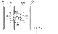
電磁界センサ部10は、直交する3つの方向に組み合わされた電磁界センサ11、12および13によって構成されている。電磁界センサ11は、図1に示すように、導体ループ13aおよび導体ループ13bとを有している。導体ループ11aおよび導体ループ11bは、図1に示すx軸に直交する単一平面内において、z軸方向に並んで配置されている。これにより、電磁界センサ11は、x軸方向の磁界およびz軸方向の電界を検出する。同様に、電磁界センサ12は、図1に示すように、導体ループ12aおよび導体ループ12bとを有している。導体ループ12aおよび導体ループ12bは、図1に示すy軸に直交する単一平面内において、x軸方向に並んで配置されている。これにより、電磁界センサ12は、y軸方向の磁界およびx軸方向の電界を検出する。電磁界センサ13は、図1に示すように、導体ループ13aおよび導体ループ13bとを有している。導体ループ13aおよび導体ループ13bは、図1に示すz軸に直交する単一平面内において、y軸方向に並んで配置されている。これにより、電磁界センサ13は、z軸方向の磁界およびy軸方向の電界を検出する。
The electromagnetic
また、電磁界センサ11、12および13の交差する位置には、回路ボックス111が配置されている。回路ボックス111には、後述するように、電磁界センサ11、12および13の一部を構成する抵抗、配線、出力端子が設けられている。
Further, a
なお、電磁界センサ部10は、電磁界センサ11、12および13をそれぞれ単独で用いたものであってもよいし、2つまたは上述したように3つを組み合わせたものであってもよい。
The electromagnetic
信号処理部20は、電磁界センサ部10において検出された電界および磁界からポインティングベクトルを計算する。信号処理部20は、例えば、アナログ値の信号をデジタル値に変換するAD変換部(図示せず)と、演算部(図示せず)とを有している。演算部は、例えばMPU(Micro Processing Unit)である。なお、演算部は、MPUに限定されることなく、他の演算回路であってもよい。
The
信号処理部20は、AD変換部により電磁界センサ部10で計測された電界および磁界(アナログ値)をサンプリングしデジタル値に変換する。そして、デジタル値に変換された電界および磁界を用いて、演算部により後述するポインティングベクトルの計算を行う。なお、信号処理部20の構成は一般的なものであるため、詳細な説明は省略する。信号処理部20の構成は、上述した構成に限らず他の構成であってもよい。
The
配線30は、電磁界センサ部10における電磁界センサ11、12および13と信号処理部20とを接続する配線である。より詳細には、配線30は、電磁界センサ部10の回路ボックス111から信号処理部20へと配線されている。電磁界センサ11、12および13で検出された電界信号および磁界信号は、配線30を介して信号処理部20に出力される。なお、配線30は、電磁界センサ11、12および13それぞれに設けてもよいし、1つの配線30を電磁界センサ11、12および13のいずれにも接続されるように設けてもよい。また、配線30に代えて、無線により電磁界センサ部10で検出された電界および磁界を信号処理部20へ出力してもよい。
The
[電磁界センサの構成]
ここで、電磁界センサ11、12および13の構成の詳細について、図2を用いて説明する。図2は、本実施の形態にかかる電磁界センサ11、12および13の概略構成図である。なお、電磁界センサ11、12および13の構成は同一であるため、以下では電磁界センサ13を例として説明する。
[Electromagnetic field sensor configuration]
Here, the details of the configuration of the
上述したように、電磁界センサ13は、導体ループ13aと導体ループ13bとを有している。
As described above, the
図2に示すように、導体ループ13aは、導線130a、抵抗132aおよび抵抗133aを有している。抵抗132aおよび抵抗133aは、導線130aの両端を接続するように、導線130aの両端の間に直列に設けられている。
As shown in FIG. 2, the
具体的には、導線130aは、直径1mmの銅線により、図2に示すように、x軸方向に長尺な矩形状の略環状に形成されている。ここで、略環状とは、完全に綴じられた環ではなく、全体として環の形状をしているが一部が開放されている形状をいう。導線130aの長辺の長さは例えば105mm、短辺の長さは例えば50mmである。また、導線130aの両端は、2つの長辺のうちの一方の中央付近において対向している。導線130aの対向する両端の間隔は、例えば5mmである。そして、対向する両端の間に、抵抗132aおよび133aが直列に配置されている。
Specifically, the
同様に、導体ループ13bは、導線130b、抵抗132bおよび133bを有している。抵抗132bおよび抵抗133bは、導線130bの両端を接続するように、導線130bの両端の間に直列に設けられている。つまり、図2に示すように、導線130bは、x軸方向に長尺な矩形状の略環状に形成されており、2つの長辺のうちの一方の中央付近において両端が対向している。そして、対向する両端の間に、抵抗132bおよび抵抗133bが直列に配置されている。
Similarly, the
また、導体ループ13aと導体ループ13bとは、対称の構成をしている。つまり、導線130aと130bは、それぞれ同一の形状であり、例えば5mmの距離を設けて点対称および線対称に配置されている。抵抗132a、132b、133aおよび133bは、それぞれ同一の形状であり、点対称および線対称に配置されている。また、抵抗132a、132b、133aおよび133bの抵抗値は、同一であり、例えば500Ωである。
Further, the
なお、導線130aと130bは、同一の形状でなくてもよいし、点対称および線対称に配置されていなくてもよい。また、導線130aと130bは、点対称および線対称のいずれかに配置されていてもよい。抵抗132a、132b、133aおよび133bは、それぞれ同一の形状でなくてもよく、点対称および線対称に配置されていなくてもよい。また、抵抗132a、132b、133aおよび133bは、点対称および線対称のいずれかに配置されていてもよい。また、抵抗132a、132b、133aおよび133bの抵抗値は、同一でなくてもよい。
The
導体ループ13aの抵抗132aと133aとの間、および、導体ループ13bの抵抗132bと133bとの間には、抵抗135が接続されている。つまり、抵抗135により、導体ループ13aと導体ループ13bとが接続されている。抵抗135は、例えば1MΩである。抵抗132a、132b、133a、133bおよび135は、回路ボックス111の内部に配置されている。
A
なお、本実施の形態において、抵抗135は、第1の抵抗に相当する。抵抗132aと133aとの和、および、抵抗132bと133bとの和は、それぞれ第2の抵抗に相当する。抵抗132aおよび133aは、それぞれ第3の抵抗に相当する。抵抗132bおよび133bは、それぞれ第4の抵抗に相当する。
In the present embodiment, the
また、導線130aと抵抗132aとの間には端子A、導線130aと抵抗133aとの間には端子A’が設けられている。つまり、抵抗132aにおいて、抵抗135が接続された一端と反対側の他端側に端子Aが設けられている。また、抵抗133aにおいて、抵抗135が接続された一端と反対側の他端側に端子A’が設けられている。端子Aと端子A’との間の電圧を検出することにより、抵抗132aおよび133aにかかる電圧を検出することができる。これにより、導体ループ13aのループ面に垂直に通過する磁界、つまり、導体ループ13aを横切る磁界を計測する。なお、導体ループ13aのループ面とは、導体ループ13aにより形成される平面のことをいう。
Further, a terminal A is provided between the
同様に、導線130bと抵抗132bとの間には端子B、導線130bと抵抗133bとの間には端子B’が設けられている。つまり、抵抗132bにおいて、抵抗135が接続された一端と反対側の他端側に端子Bが設けられている。また、抵抗133bにおいて、抵抗135が接続された一端と反対側の他端側に端子B’が設けられている。端子Bと端子B’との間の電圧を検出することにより、抵抗132bおよび133bにかかる電圧を検出することができる。これにより、導体ループ13bのループ面に垂直に通過する磁界を計測する。
Similarly, a terminal B is provided between the
また、抵抗135の両端には、それぞれ端子Cおよび端子C’が設けられている。端子Cと端子C’との間の電圧を検出することにより、抵抗135にかかる電圧を検出することができる。これにより、導体ループ13aと13bとの間の電界を計測する。
Further, terminals C and terminals C'are provided at both ends of the
なお、本実施の形態において、端子Cと端子C’との間の電圧は、第1の電圧に相当する。また、端子Aと端子A’との間の電圧、および、端子Bと端子B’との間の電圧は、それぞれ第2の電圧に相当する。 In this embodiment, the voltage between the terminal C and the terminal C'corresponds to the first voltage. Further, the voltage between the terminal A and the terminal A'and the voltage between the terminal B and the terminal B'correspond to the second voltage, respectively.
電磁界センサ11および12は、電磁界センサ13と同様の構成であるため、詳細な説明は省略する。
Since the
このような構成により、電磁界センサ部10により、例えば150kHz〜30MHz程度の周波数の電磁界を計測することができる。なお、上述した導線130aおよび130bの大きさ、抵抗132a、132b、133a、133bおよび135の値を変更することにより、検出可能な電磁界の周波数帯域を変更してもよい。
With such a configuration, the electromagnetic
なお、電磁界センサ11、12および13は上述したように同一の構成としてもよいし、電磁界センサ11、12および13のうちの2つのみが同一の構成であってもよい。また、電磁界センサ11、12および13のすべてが異なる構成であってもよい。
The
[電磁界計測の原理]
次に、電磁界計測システム1による電磁界計測の原理について図3を用いて説明する。図3は、本実施の形態にかかる電磁界センサ11、12および13における電界および磁界の計測位置を示す図であり、(a)は電磁界センサ13における電界および磁界の計測位置を示す図、(b)は(a)に示した電磁界センサ13における座標軸と電磁界センサ13における電界および磁界の方向を示す図である。
[Principle of electromagnetic field measurement]
Next, the principle of electromagnetic field measurement by the electromagnetic
電界は2つの導体間の単位長さ当たりの電位差であるので、電磁界計測システム1では、電磁界センサ13における2つの導体である導体ループ13aと導体ループ13bとの電位差を計測する。
Since the electric field is the potential difference per unit length between the two conductors, the electromagnetic
具体的には、電磁界センサ13において、電界は、図3の(a)に示すように、電磁界センサ13の中心P、すなわち、導体ループ13aと導体ループ13bとの間に生じる電位差を検出することにより計測する。つまり、電磁界センサ13では、電界は、抵抗135にかかる電圧を検出し計算(校正)することにより得られる。より具体的には、電磁界センサ13において端子Cと端子C’との間の電圧を検出する。そして、検出された電圧を用いて、後述する校正を行う。これにより、電磁界センサ13は、図3の(b)に示すようにy軸方向の電界Eyを計測することができる。
Specifically, in the
なお、抵抗135は、導体ループ13aと導体ループ13bとの間の電圧を検出しやすくするために設けられたものであり、導体ループ13aと導体ループ13bとの間の電圧を検出することができるのであれば、抵抗135を設けない構成としてもよい。
The
また、電磁界センサ13と同様に、電磁界センサ11および12は、それぞれz軸方向の電界およびx軸方向の電界を計測する。電磁界センサ11、12および13を組み合わせることにより、x軸方向、y軸方向およびz軸方向のそれぞれの電界Ex、EyおよびEzを同時に計測することができる。また、電磁界センサ11、12および13の構成を同一の構成とし、それぞれの中心で交叉させて、導体ループ13aおよび13bが配置された平面が互いに直交するように組み合わせることにより、同一位置における電界Ex、EyおよびEzを同時に計測することができる。
Further, similarly to the
また、電磁界計測システム1では、電磁界センサ13における2つの導体である導体ループ13aおよび導体ループ13bのそれぞれのループ面に鎖交する磁界を、導体ループ13aおよび導体ループ13bそれぞれの電圧を計測することにより計測する。ここで、ループ面に鎖交する磁界とは、ループ面を垂直に横切る磁束、すなわち、導体ループ13aおよび導体ループ13bのループ面を垂直に横切る磁界をループ面積で積分(平均)したものをいう。ループ面に鎖交する磁界のことを、ループの中心の磁界ということもある。
Further, in the electromagnetic
具体的には、電磁界センサ13において、図3の(a)に示すように、導体ループ13aと導体ループ13bのそれぞれのループの端子間における電圧を検出し、導体ループ13aと導体ループ13bのそれぞれのループ面に鎖交する磁界を計算(校正)する。そして、導体ループ13aと導体ループ13bのそれぞれのループ面に鎖交する磁界を平均することにより、電磁界センサ13の中心の磁界を計測することができる。なお、電磁界センサ13では、導体ループ13aと導体ループ13bのそれぞれのループの端子間で検出された電圧の平均値から、電磁界センサ13における磁界を計算してもよい。
Specifically, as shown in FIG. 3A, the
電磁界センサ13において、導体ループ13aのループ面に鎖交する磁界は、抵抗132aおよび133aにかかる電圧を検出し計算することにより得られる。また、導体ループ13bのループ面に鎖交する磁界は、抵抗132bおよび133bにかかる電圧を検出し計算することにより得られる。より具体的には、導体ループ13aのループ面に鎖交する磁界は、端子Aと端子A’との間の電圧を検出して計算することにより得られる。導体ループ13bのループ面に鎖交する磁界は、端子Bと端子B’との間の電圧を検出して計算することにより得られる。そして、端子Aと端子A’との間の電圧と端子Bと端子B’との間の電圧との平均を計算する。すなわち、端子Aと端子A’との間の電圧と端子Bと端子B’との間の電圧とを用いて後述する校正を行うことにより、導体ループ13aと導体ループ13bとの間で導体ループ13aと導体ループ13bとから等しい距離にある点Pにおける磁界、つまり、電磁界センサ13における磁界が得られる。
In the
これにより、電磁界センサ13は、図3の(b)に示すようにz軸方向の磁界Hzを計測することができる。
Thus, the
なお、抵抗132aおよび133aは、導体ループ13aのループ面に鎖交する磁界を計測するための電圧を検出しやすくするために設けられた抵抗である。また、抵抗132bおよび133bは、導体ループ13bのループ面に鎖交する磁界を計測するための電圧を検出しやすくするために設けられた抵抗である。導体ループ13aおよび導体ループ13bのそれぞれのループ面に鎖交する磁界を計測するための電圧を検出することができるのであれば、抵抗132a、133a、132bおよび133bを設けない構成としてもよい。
The
また、電磁界センサ13と同様に、電磁界センサ11および12は、それぞれx軸方向の磁界およびy軸方向の磁界を計測する。電磁界センサ11、12および13を組み合わせることにより、x軸方向、y軸方向およびz軸方向のそれぞれの磁界Hx、HyおよびHzを同時に計測することができる。また、電磁界センサ11、12および13の構成を同一の構成とし、それぞれの中心位置において組み合わせることにより、同一位置における磁界Hx、HyおよびHzを同時に計測することができる。
Further, similarly to the
ここで、電磁界の校正の手順について説明する。 Here, the procedure for calibrating the electromagnetic field will be described.
まず、電磁界センサ11、12および13のそれぞれにおいてループの端子間に生じる電圧を検出するために、基準電界または基準磁界を電磁界センサ11、12および13のそれぞれに印加する。そして、電磁界センサ11、12および13のそれぞれにおいて、ループの端子間に生じる電圧を計測する。これにより、電磁界センサ11、12および13のそれぞれについて、電界または磁界と検出される電圧との関係、すなわち、アンテナ係数が得られる。
First, a reference electric field or a reference magnetic field is applied to the
そして、電磁界センサ11、12および13のそれぞれにおいて実際に検出された電圧にアンテナ係数を乗算し、電磁界センサ11、12および13で計測された電界または磁界を計算する。
Then, the voltage actually detected by the
なお、検出された電圧に、出力されるはずのない成分の電圧が含まれている場合には、電磁界センサ11、12および13の各成分の間でクロストークが生じていることになる。なお、成分とは、x軸方向、y軸方向およびz軸方向のそれぞれに対応する電界(Ex、Ey、Ez)および磁界(Hx、Hy、Hz)のことをいう。クロストークの有無、および、クロストークが発生している成分を検出することより、各電磁界センサの性能を評価することができる。
If the detected voltage includes a voltage of a component that should not be output, crosstalk occurs between the components of the
また、x軸方向、y軸方向およびz軸方向それぞれの電界(Ex、Ey、Ez)および磁界(Hx、Hy、Hz)を印加したときの、各軸方向の電界および磁界に対応する6成分の出力電圧は、6×6行列の形で表すことができる。この行列を用いることで、実際に計測された6成分の出力電圧から、電磁界センサ11、12および13で検出された電磁界6成分を精度よく求めることができる。
Further, when an electric field (Ex , E y , E z ) and a magnetic field (H x , Hy , H z ) in the x-axis direction, the y-axis direction, and the z-axis direction are applied, the electric field in each axial direction and The output voltage of the six components corresponding to the magnetic field can be expressed in the form of a 6 × 6 matrix. By using this matrix, the electromagnetic field 6 components detected by the
また、電磁界計測システム1は、上述したように、同一位置における電界および磁界を同時に計測することができるため、計測した電界および磁界を用いて信号処理部20においてポインティングベクトルを計算してもよい。ポインティングベクトルは、電磁界のエネルギー密度の流れを示す指標であり、ポインティングベクトルの方向は電磁界のエネルギーの移動方向を表す。
Further, since the electromagnetic
ポインティングベクトルは、電界ベクトルを
![]()
![]()
![]()
![]()
![]()
![]()
より詳細には、電界ベクトルおよび磁界ベクトルは時間により変化するものであり、ある瞬間(時刻t)におけるポインティングベクトル(瞬時ポインティングベクトル)は、以下の(式4)のように表される。 More specifically, the electric field vector and the magnetic field vector change with time, and the pointing vector (instantaneous pointing vector) at a certain moment (time t) is expressed as follows (Equation 4).
![]()
![]()
ここで、E(t)およびH(t)は、それぞれ時刻tにおける電界ベクトルおよび磁界ベクトルを示している。 Here, E (t) and H (t) indicate an electric field vector and a magnetic field vector at time t, respectively.
この瞬時ポインティングベクトルにより、ある時刻tにおける電磁界のエネルギーおよび電磁界のエネルギーの移動方向を検出することができる。 With this instantaneous pointing vector, the energy of the electromagnetic field and the moving direction of the energy of the electromagnetic field at a certain time t can be detected.
また、瞬時ポインティングベクトルを一定時間計測し、平均値を計算することにより、ポインティングベクトルの時間平均を計測することができる。ポインティングベクトルの時間平均は、電磁波源から放射されるエネルギーの伝搬方向を示す。したがって、ポインティングベクトルを計算することにより、電磁波源から放射されるエネルギーの伝搬方向を検出することができる。 Further, the time average of the pointing vector can be measured by measuring the instantaneous pointing vector for a certain period of time and calculating the average value. The time average of the pointing vector indicates the propagation direction of the energy radiated from the electromagnetic wave source. Therefore, by calculating the pointing vector, the propagation direction of the energy radiated from the electromagnetic wave source can be detected.
なお、ポインティングベクトルの計算は、上述したように時間軸において行ってもよいし、周波数軸において行ってもよい。 The calculation of the pointing vector may be performed on the time axis or the frequency axis as described above.
以上のポインティングベクトルの計算を信号処理部20において行うことにより、電磁界計測システム1は、ある時刻tにおける電磁界センサ部10の位置での電界および磁界を計測することができる。さらに、信号処理部20により、電磁界センサ部10が配置された位置における電界および磁界の計測結果から、不要電磁波の伝搬経路および電磁波源を推定してもよい。例えば、直交偏波を持つ平面波に対しては、x軸方向の磁界Hx、y軸方向の磁界Hyおよびz軸方向の電界Ezからx−y平面の角度を検出することができる。同様に、y軸方向の磁界Hy、z軸方向の磁界Hzおよびx軸方向の電界Exからy−z平面の角度を検出することができる。z軸方向の磁界Hz、x軸方向の磁界Hxおよびy軸方向の電界Eyからz−x平面の角度を検出することができる。また、これらのx−y平面、y−z平面およびz−x平面の角度を組み合わせることにより電磁波源の位置を推定してもよい。
By performing the above calculation of the pointing vector in the
また、信号処理部20は、電磁界センサ部10において検出された電界および磁界の向きからポインティングベクトルを計算してもよい。例えば、上述した電界および磁界の校正を、電界の絶対値Ex、Ey、Ezおよび磁界の絶対値Hx、Hy、Hzではなく電界の相対値aEx、aEy、aEz(aは係数)および磁界の相対値bHx、bHy、bHz(bは係数)を用いて計算してもよい。これにより、少なくとも電磁波源の位置に関する角度情報を検出することができるので、電磁波源の方向を推定することができる。
Further, the
このように、電磁界センサ部10および信号処理部20は、電磁波の到来方向を推定する電磁波の到来方向推定システムとして用いてもよい。
As described above, the electromagnetic
なお、電磁界の変化により導体ループ13aおよび13bを流れる電流は微小であるため、電磁界センサ部10において検出される電界計測のための電圧および磁界計測のための電圧は微小である。したがって、電磁界センサ11、12および13により検出したこれらの電圧をアンプにより増幅して信号処理部20に出力してもよい。
Since the current flowing through the
[効果等]
以上、本実施の形態にかかる電磁界センサおよび電磁界計測システムによると、同一の位置での電界および磁界を検出することができるので、ポインティングベクトルを計測することができる。したがって、電磁界センサが配置された位置における電界および磁界を計測することができる。さらに、信号処理部20により、電磁界センサが配置された位置における電界および磁界を計測した結果から、不要電磁波の伝搬経路および電磁波源を推定してもよい。
[Effects, etc.]
As described above, according to the electromagnetic field sensor and the electromagnetic field measurement system according to the present embodiment, the electric field and the magnetic field at the same position can be detected, so that the pointing vector can be measured. Therefore, it is possible to measure the electric field and the magnetic field at the position where the electromagnetic field sensor is arranged. Further, the
(実施の形態2)
次に、実施の形態2にかかる電磁界計測システム2について、図4〜図6を用いて説明する。図4は、本実施の形態にかかる電磁界計測システム2の概略構成図である。図5は、本実施の形態にかかる電磁界計測システム2における第1のアンプ31の概略構成図である。図6は、本実施の形態にかかる電磁界計測システム2における第2のアンプ32の概略構成図である。
(Embodiment 2)
Next, the electromagnetic
本実施の形態にかかる電磁界計測システム2が実施の形態1に示した電磁界計測システム1と異なる点は、電磁界センサ部10と信号処理部20との間に第1のアンプ31と第2のアンプ32とを備える点である。
The difference between the electromagnetic
図4に示すように、電磁界計測システム2は、実施の形態1に示した電磁界計測システム1と同様、電磁界センサ部10と、信号処理部20と、配線30とを備えている。また、配線30には第1のアンプ31と第2のアンプ32が設けられている。なお、電磁界センサ部10および信号処理部20の基本的な構成については実施の形態1に示した電磁界計測システム1における電磁界センサ部10および信号処理部20と同様であるため、詳細な説明を省略する。
As shown in FIG. 4, the electromagnetic
第1のアンプ31は、電磁界センサ部10から、電界を計測するための電圧を増幅して出力するための電界プリアンプである。つまり、第1のアンプ31は、端子CおよびC’に接続される。図5に示すように、第1のアンプ31は、端子Cが接続された増幅器34aと、端子C’が接続された増幅器34bと、端子Cと増幅器34aとの間においてグランドに接続された抵抗35aと、端子C’と増幅器34bとの間においてグランドに接続された抵抗35bと、増幅器34および34bから出力された電圧が入力される増幅器36とを有している。
The
増幅器36は、端子Cにおける電圧VCを増幅器34aで増幅した電圧と、端子C’における電圧VC’を増幅器34bで増幅した電圧との差を増幅して出力する。したがって、第1のアンプ31からは、端子Cと端子C’の電位差VC−VC’に比例する電圧が出力される。第1のアンプ31から出力される電圧を用いて、導体ループ13aと13bとの間における電界を計算することができる。これにより、端子Cにおける電圧VCおよび端子C’における電圧VC’の値が微小である場合であっても、電磁界センサ部10により電界を精度よく計測することができる。
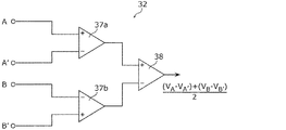
第2のアンプ32は、電磁界センサ部10から、磁界を計測するための電圧を増幅して出力するための磁界プリアンプである。第2のアンプ32は、端子AおよびA’と、端子BおよびB’に接続される。図6に示すように、第2のアンプ32は、端子AおよびA’が接続された増幅器37aと、端子BおよびB’が接続された増幅器37bと、増幅器37aおよび37bから出力された電圧が入力される増幅器38とを有している。
The
増幅器37aは、端子Aにおける電圧VAと端子A’における電圧VA’との差VA−VA’を増幅して出力する。増幅器37bは、端子Bにおける電圧VBと端子B’における電圧VB’との差VB−VB’を増幅して出力する。増幅器38は、増幅器37aにおいて電位差VA−VA’が増幅された電圧と、増幅器37bにおいて電位差VB−VB’が増幅された電圧とを加算して出力する。第2のアンプ32からは、端子Aと端子A’の電位差VA−VA’と端子Bと端子B’の電位差VB−VB’とに比例する電圧の平均値が出力される。
第2のアンプ32から出力された電圧を用いて計算することにより、導体ループ13aにおいて検出される磁界と導体ループ13bにおいて検出される磁界との平均、すなわち、導体ループ13aと13bとの間における磁界を計算することができる。これにより、端子Aにおける電圧VA、端子A’における電圧VA’、端子Bにおける電圧VBおよび端子B’における電圧VB’の値が微小である場合であっても、電磁界センサ部10により磁界を精度よく計測することができる。
By calculating using the voltage output from the
なお、第1のアンプ31および第2のアンプ32は、電磁界センサ11、12および13それぞれの中心に位置するように設けられていてもよい。第1のアンプおよび第2のアンプが電磁界センサ11、12および13の中心に位置していない場合、電磁界センサ11、12および13からアンプまでの配線30の長さおよび引き回し位置が非対称となり、電磁界センサ11、12および13の各ループにおける電磁界を乱す可能性があるためである。第1のアンプおよび第2のアンプが電磁界センサ11、12および13の中心に位置するように設けられることにより、各電磁波センサにおいて2つのループの電界および磁界の対称性を保つことができるので、電磁界の計測精度を向上することができる。例えば、第1のアンプ31および第2のアンプ32は、電磁界センサ部10の回路ボックス111の内部に設けられていてもよい。
The
(その他の実施の形態)
以上、本発明にかかる電磁界センサおよび電磁界計測システムについて、実施の形態に基づいて説明したが、本発明は実施の形態に限定されるものではない。実施の形態に対して当業者が思いつく変形を施して得られる形態、および、複数の実施の形態における構成要素を任意に組み合わせて実現される別の形態も本発明に含まれる。
(Other embodiments)
Although the electromagnetic field sensor and the electromagnetic field measurement system according to the present invention have been described above based on the embodiments, the present invention is not limited to the embodiments. The present invention also includes a form obtained by subjecting an embodiment to a modification that a person skilled in the art can think of, and another form realized by arbitrarily combining components in a plurality of embodiments.
例えば、上述した実施の形態では、電磁界センサ部は、3つの電磁界センサを、各電磁界センサが配置された単一平面が互いに直交するように組み合わせた構成としたが、電磁界センサ部は1つの電磁界センサで構成されてもよいし、2つの電磁界センサで構成されてもよい。 For example, in the above-described embodiment, the electromagnetic field sensor unit has a configuration in which three electromagnetic field sensors are combined so that the single planes on which the electromagnetic field sensors are arranged are orthogonal to each other. May be composed of one electromagnetic field sensor or may be composed of two electromagnetic field sensors.
また、上述した実施の形態では、電磁界センサを構成する導体ループは、矩形状としたが、矩形状に限らず、例えば円形状など他の形状であってもよい。また、電磁界センサを構成する一対の導体ループの形状は、同一の形状であってもよいし異なる形状であってもよい。また、一対の導体ループの配置は、点対称および線対称、または、点対称および線対称のいずれかに配置されてもよいし、他の配置であってもよい。 Further, in the above-described embodiment, the conductor loop constituting the electromagnetic field sensor has a rectangular shape, but the conductor loop is not limited to a rectangular shape, and may have another shape such as a circular shape. Further, the shape of the pair of conductor loops constituting the electromagnetic field sensor may be the same shape or different shapes. Further, the arrangement of the pair of conductor loops may be either point-symmetrical and line-symmetrical, or point-symmetrical and line-symmetrical, or may be another arrangement.
また、一対の導体ループの一部を構成する複数の抵抗は、同一の抵抗値であってもよいし異なる抵抗値であってもよい。また、一対の導体ループを接続する抵抗は、導体ループの一部を構成する抵抗と同一の抵抗値であってもよいし、異なる抵抗値であってもよい。 Further, the plurality of resistors forming a part of the pair of conductor loops may have the same resistance value or different resistance values. Further, the resistance connecting the pair of conductor loops may have the same resistance value as the resistance forming a part of the conductor loop, or may have a different resistance value.
さらに、電磁界計測システムは、電界を計測するために検出する一対の導体ループ間の電圧を増幅するための第1のアンプを備えてもよいし、備えなくてもよい。また、電磁界計測システムは、磁界を計測するために検出する電圧を増幅するための第2のアンプを備えてもよいし、備えなくてもよい。また、第1のアンプおよび第2のアンプは、電磁界センサ部の中心に設けられてもよいし、他の位置に設けられてもよい。 Further, the electromagnetic field measurement system may or may not include a first amplifier for amplifying the voltage between the pair of conductor loops detected to measure the electric field. Further, the electromagnetic field measurement system may or may not include a second amplifier for amplifying the voltage to be detected in order to measure the magnetic field. Further, the first amplifier and the second amplifier may be provided at the center of the electromagnetic field sensor unit, or may be provided at other positions.
また、上述した実施の形態では、電磁界センサから信号処理部まで配線を設け、電磁界センサ部で検出された電界および磁界を、配線を通じて信号処理部へ出力する構成としたが、配線に代えて無線により電磁界センサで検出された電界および磁界を信号処理部へ出力してもよい。 Further, in the above-described embodiment, wiring is provided from the electromagnetic field sensor to the signal processing unit, and the electric field and the magnetic field detected by the electromagnetic field sensor unit are output to the signal processing unit through the wiring. The electric field and the magnetic field detected by the electromagnetic field sensor wirelessly may be output to the signal processing unit.
また、電磁界計測システムにおいて、信号処理部は、上述したようにAD変換部および演算部を備える構成であってもよいし、他の構成であってもよい。また、信号処理部は、計測した電界および磁界、計算したポインティングベクトルを記憶する記憶部をさらに備えてもよい。 Further, in the electromagnetic field measurement system, the signal processing unit may have an AD conversion unit and a calculation unit as described above, or may have another configuration. Further, the signal processing unit may further include a storage unit that stores the measured electric field and magnetic field and the calculated pointing vector.
本発明にかかる電磁界センサおよび電磁界計測システムは、広帯域の周波数の電磁波を検出することが必要な鉄道、車などに用いられる電磁界センサおよび電磁界計測システムとして有用である。 The electromagnetic field sensor and electromagnetic field measurement system according to the present invention are useful as electromagnetic field sensors and electromagnetic field measurement systems used in railways, vehicles, etc., which need to detect electromagnetic waves having a wide band frequency.
1、2 電磁界計測システム
10 電磁界センサ部
11、12、13 電磁界センサ
11a、11b、12a、12b、13a、13b 導体ループ
20 信号処理部
30 配線
31 第1のアンプ
32 第2のアンプ
34a、34b、36、37a、37b、38 増幅器
35a、35b 抵抗
111 回路ボックス
130a、130b 導線
132a、132b 抵抗(第2の抵抗、第3の抵抗)
133a、133b 抵抗(第2の抵抗、第4の抵抗)
135 抵抗(第1の抵抗)
1, 2 Electromagnetic
133a, 133b resistance (second resistance, fourth resistance)
135 resistance (first resistance)
Claims (9)
前記一対の導体ループは、互いに第1の抵抗により接続されており、
前記第1の抵抗の両端の電圧である第1の電圧を検出することにより電界を計測する
電磁界センサ。 With a pair of conductor loops arranged in a single plane
The pair of conductor loops are connected to each other by a first resistor.
An electromagnetic field sensor that measures an electric field by detecting a first voltage, which is a voltage across the first resistor.
請求項1に記載の電磁界センサ。 The electromagnetic field sensor according to claim 1, wherein each conductor loop of the pair of conductor loops has the same shape and is arranged symmetrically.
前記一対の導体ループの各導体ループは、当該導体ループの一部として第2の抵抗を有し、
前記第2の抵抗の両端の電圧である第2の電圧を検出することにより磁界を計測し、
前記一対の導体ループの各導体ループは、第1の抵抗により接続されており、
前記第2の抵抗は、抵抗値が等しく直列に接続された第3の抵抗および第4の抵抗とで構成され、
前記第3の抵抗と第4の抵抗との間に、前記第1の抵抗が接続されており、
前記第1の抵抗の両端の電圧である第1の電圧を検出することにより電界を計測し、
前記第1の抵抗が接続された前記第3の抵抗の一端と反対側の前記第3の抵抗の他端と、前記第1の抵抗が接続された前記第4の抵抗の一端と反対側の前記第4の抵抗の他端との間の電圧である前記第2の電圧を検出することにより磁界を計測する
電磁界センサ。 With a pair of conductor loops arranged in a single plane
Each conductor loop of the pair of conductor loops has a second resistor as part of the conductor loop.
The magnetic field is measured by detecting the second voltage, which is the voltage across the second resistor.
Each conductor loop of the pair of conductor loops is connected by a first resistor.
The second resistor is composed of a third resistor and a fourth resistor having equal resistance values and connected in series.
The first resistor is connected between the third resistor and the fourth resistor.
The electric field is measured by detecting the first voltage, which is the voltage across the first resistor.
The other end of the third resistor opposite to one end of the third resistor to which the first resistor is connected, and the other end of the fourth resistor to which the first resistor is connected are opposite to each other. The magnetic field is measured by detecting the second voltage, which is the voltage between the fourth resistor and the other end.
Magnetic field sensor power.
請求項1または3に記載の電磁界センサ。 The electromagnetic field sensor according to claim 1 or 3 , further comprising a first amplifier that amplifies and outputs the first voltage.
請求項3に記載の電磁界センサ。 The third aspect of claim 3, further comprising a second amplifier that amplifies the second voltage detected in each conductor loop of the pair of conductor loops and outputs the average value of the amplified second voltage. Electromagnetic field sensor.
前記3組の電磁界センサがそれぞれ配置された前記単一平面は互いに直交し、かつ、前記3組の電磁界センサは、前記3組の電磁界センサそれぞれの中心で交叉している
請求項1〜5のいずれか1項に記載の電磁界センサ。 It has three sets of the electromagnetic field sensors.
The single plane on which the three sets of electromagnetic field sensors are arranged is orthogonal to each other, and the three sets of electromagnetic field sensors intersect at the center of each of the three sets of electromagnetic field sensors. The electromagnetic field sensor according to any one of 5 to 5.
前記電磁界センサにおいて検出された前記電界および前記磁界からポインティングベクトルを計算する信号処理部とを備える
電磁界計測システム。 The electromagnetic field sensor according to claim 3 and
An electromagnetic field measurement system including the electric field detected by the electromagnetic field sensor and a signal processing unit that calculates a pointing vector from the magnetic field.
前記電磁界センサにおいて検出された前記電界および前記磁界の少なくとも一部からポインティングベクトルを計算する信号処理部とを備え、
前記信号処理部は、計算した前記ポインティングベクトルから電磁波の到来方向を推定する
電磁波の到来方向推定システム。 The electromagnetic field sensor according to claim 3 and
It includes a signal processing unit that calculates a pointing vector from the electric field detected by the electromagnetic field sensor and at least a part of the magnetic field.
The signal processing unit is an electromagnetic wave arrival direction estimation system that estimates the electromagnetic wave arrival direction from the calculated pointing vector.
前記電磁界センサにおいて検出された前記電界の向きおよび前記磁界の向きからポインティングベクトルを計算する信号処理部とを備え、
前記信号処理部は、計算した前記ポインティングベクトルから電磁波の到来方向を推定する
電磁波の到来方向推定システム。 The electromagnetic field sensor according to claim 3 and
It is provided with a signal processing unit that calculates a pointing vector from the direction of the electric field and the direction of the magnetic field detected by the electromagnetic field sensor.
The signal processing unit is an electromagnetic wave arrival direction estimation system that estimates the electromagnetic wave arrival direction from the calculated pointing vector.
Priority Applications (1)
| Application Number | Priority Date | Filing Date | Title |
|---|---|---|---|
| JP2016247023A JP6944672B2 (en) | 2016-12-20 | 2016-12-20 | Electromagnetic field sensor, electromagnetic field measurement system and electromagnetic wave arrival direction estimation system |
Applications Claiming Priority (1)
| Application Number | Priority Date | Filing Date | Title |
|---|---|---|---|
| JP2016247023A JP6944672B2 (en) | 2016-12-20 | 2016-12-20 | Electromagnetic field sensor, electromagnetic field measurement system and electromagnetic wave arrival direction estimation system |
Publications (2)
| Publication Number | Publication Date |
|---|---|
| JP2018100904A JP2018100904A (en) | 2018-06-28 |
| JP6944672B2 true JP6944672B2 (en) | 2021-10-06 |
Family
ID=62715259
Family Applications (1)
| Application Number | Title | Priority Date | Filing Date |
|---|---|---|---|
| JP2016247023A Active JP6944672B2 (en) | 2016-12-20 | 2016-12-20 | Electromagnetic field sensor, electromagnetic field measurement system and electromagnetic wave arrival direction estimation system |
Country Status (1)
| Country | Link |
|---|---|
| JP (1) | JP6944672B2 (en) |
Families Citing this family (3)
| Publication number | Priority date | Publication date | Assignee | Title |
|---|---|---|---|---|
| JP7410561B2 (en) | 2020-02-28 | 2024-01-10 | 国立大学法人金沢大学 | Radio wave sensor and electric field component detection device |
| JPWO2022196573A1 (en) * | 2021-03-15 | 2022-09-22 | ||
| WO2023166228A1 (en) * | 2022-03-04 | 2023-09-07 | eV-Technologies | Device and method for simultaneous detection of incident electric and magnetic fields, as well as energy crossing a given surface |
Family Cites Families (9)
| Publication number | Priority date | Publication date | Assignee | Title |
|---|---|---|---|---|
| DE59203328D1 (en) * | 1991-02-25 | 1995-09-28 | Asea Brown Boveri | Field strength meter. |
| JPH09166653A (en) * | 1995-12-18 | 1997-06-24 | Ricoh Co Ltd | Coil for magnetic-flux detection and magnetic-flux detection probe |
| JP4925232B2 (en) * | 2001-02-02 | 2012-04-25 | 株式会社バッファロー | Electric field probe |
| JP5151032B2 (en) * | 2006-01-13 | 2013-02-27 | 株式会社日立製作所 | Magnetic field probe device and magnetic field probe element |
| JP2008128847A (en) * | 2006-11-21 | 2008-06-05 | Murata Mfg Co Ltd | Measuring device |
| KR20100034449A (en) * | 2008-09-24 | 2010-04-01 | 삼성전자주식회사 | Probe of electrical measuring instrument |
| CA2777814C (en) * | 2009-10-16 | 2018-03-27 | David Jackson | Electromagnetic field detection systems and methods |
| JP6042693B2 (en) * | 2012-10-22 | 2016-12-14 | 株式会社日本自動車部品総合研究所 | Pointing vector measuring device |
| WO2016189999A1 (en) * | 2015-05-22 | 2016-12-01 | 三菱電機株式会社 | Electromagnetic field probe |
-
2016
- 2016-12-20 JP JP2016247023A patent/JP6944672B2/en active Active
Also Published As
| Publication number | Publication date |
|---|---|
| JP2018100904A (en) | 2018-06-28 |
Similar Documents
| Publication | Publication Date | Title |
|---|---|---|
| JP5616431B2 (en) | Method for estimating the amount of current by detecting the magnetic field generated from the current | |
| US8378675B2 (en) | Current sensor, current measuring module and method for measuring current | |
| JP4626728B2 (en) | Magnetic detector | |
| EP3508863B1 (en) | Offset current sensor structure | |
| US8018221B2 (en) | Apparatus for measuring an electric current flowing through an electrical conductor | |
| JP6944672B2 (en) | Electromagnetic field sensor, electromagnetic field measurement system and electromagnetic wave arrival direction estimation system | |
| US20140097826A1 (en) | Current sensor | |
| JP4635544B2 (en) | Electric field distribution measuring method and electric field distribution measuring apparatus | |
| US20150204916A1 (en) | Electric current sensor | |
| KR20150009455A (en) | Current sensor | |
| US10274521B2 (en) | Multiple sensor based Rogowski coil | |
| US20170059623A1 (en) | Non-contact sensor based rogowski coil | |
| US20180292469A1 (en) | Method and arrangement for determining the transverse sensitivity of magnetic field sensors | |
| WO2013145928A1 (en) | Current detection apparatus and current detection method | |
| JP6671985B2 (en) | Current sensor | |
| CN111033277A (en) | Hall effect current sensor | |
| US10082527B2 (en) | Removal of higher order magnetic interference in magnetic field based current sensors | |
| JPWO2018199067A1 (en) | Magnetic sensor | |
| Schneider et al. | Integrating giant magneto-resistive (GMR) field detectors for high bandwidth current sensing in power electronic modules | |
| JP2013053914A (en) | Current measuring device | |
| KR101180221B1 (en) | Current Probe Using Magneto Resistance Sensor | |
| JP6671986B2 (en) | Current sensor and method of manufacturing the same | |
| JP2021001832A (en) | Current sensor | |
| JP6881937B2 (en) | Current sensor | |
| US20140132255A1 (en) | Surface current probe |
Legal Events
| Date | Code | Title | Description |
|---|---|---|---|
| A621 | Written request for application examination |
Free format text: JAPANESE INTERMEDIATE CODE: A621 Effective date: 20191115 |
|
| A977 | Report on retrieval |
Free format text: JAPANESE INTERMEDIATE CODE: A971007 Effective date: 20200914 |
|
| A131 | Notification of reasons for refusal |
Free format text: JAPANESE INTERMEDIATE CODE: A131 Effective date: 20201006 |
|
| A521 | Written amendment |
Free format text: JAPANESE INTERMEDIATE CODE: A523 Effective date: 20201109 |
|
| A131 | Notification of reasons for refusal |
Free format text: JAPANESE INTERMEDIATE CODE: A131 Effective date: 20210316 |
|
| A521 | Written amendment |
Free format text: JAPANESE INTERMEDIATE CODE: A523 Effective date: 20210413 |
|
| TRDD | Decision of grant or rejection written | ||
| A01 | Written decision to grant a patent or to grant a registration (utility model) |
Free format text: JAPANESE INTERMEDIATE CODE: A01 Effective date: 20210817 |
|
| A61 | First payment of annual fees (during grant procedure) |
Free format text: JAPANESE INTERMEDIATE CODE: A61 Effective date: 20210902 |
|
| R150 | Certificate of patent or registration of utility model |
Ref document number: 6944672 Country of ref document: JP Free format text: JAPANESE INTERMEDIATE CODE: R150 |