JP6926018B2 - Transfer substrate, mounting method using it, and manufacturing method of image display device - Google Patents
Transfer substrate, mounting method using it, and manufacturing method of image display device Download PDFInfo
- Publication number
- JP6926018B2 JP6926018B2 JP2018061743A JP2018061743A JP6926018B2 JP 6926018 B2 JP6926018 B2 JP 6926018B2 JP 2018061743 A JP2018061743 A JP 2018061743A JP 2018061743 A JP2018061743 A JP 2018061743A JP 6926018 B2 JP6926018 B2 JP 6926018B2
- Authority
- JP
- Japan
- Prior art keywords
- transfer
- chip component
- substrate
- board
- chip
- Prior art date
- Legal status (The legal status is an assumption and is not a legal conclusion. Google has not performed a legal analysis and makes no representation as to the accuracy of the status listed.)
- Active
Links
Images


Classifications
-
- H—ELECTRICITY
- H01—ELECTRIC ELEMENTS
- H01L—SEMICONDUCTOR DEVICES NOT COVERED BY CLASS H10
- H01L33/00—Semiconductor devices with at least one potential-jump barrier or surface barrier specially adapted for light emission; Processes or apparatus specially adapted for the manufacture or treatment thereof or of parts thereof; Details thereof
- H01L33/48—Semiconductor devices with at least one potential-jump barrier or surface barrier specially adapted for light emission; Processes or apparatus specially adapted for the manufacture or treatment thereof or of parts thereof; Details thereof characterised by the semiconductor body packages
- H01L33/62—Arrangements for conducting electric current to or from the semiconductor body, e.g. lead-frames, wire-bonds or solder balls
-
- H—ELECTRICITY
- H01—ELECTRIC ELEMENTS
- H01L—SEMICONDUCTOR DEVICES NOT COVERED BY CLASS H10
- H01L2224/00—Indexing scheme for arrangements for connecting or disconnecting semiconductor or solid-state bodies and methods related thereto as covered by H01L24/00
- H01L2224/01—Means for bonding being attached to, or being formed on, the surface to be connected, e.g. chip-to-package, die-attach, "first-level" interconnects; Manufacturing methods related thereto
- H01L2224/10—Bump connectors; Manufacturing methods related thereto
- H01L2224/15—Structure, shape, material or disposition of the bump connectors after the connecting process
- H01L2224/16—Structure, shape, material or disposition of the bump connectors after the connecting process of an individual bump connector
- H01L2224/161—Disposition
- H01L2224/16151—Disposition the bump connector connecting between a semiconductor or solid-state body and an item not being a semiconductor or solid-state body, e.g. chip-to-substrate, chip-to-passive
- H01L2224/16221—Disposition the bump connector connecting between a semiconductor or solid-state body and an item not being a semiconductor or solid-state body, e.g. chip-to-substrate, chip-to-passive the body and the item being stacked
- H01L2224/16225—Disposition the bump connector connecting between a semiconductor or solid-state body and an item not being a semiconductor or solid-state body, e.g. chip-to-substrate, chip-to-passive the body and the item being stacked the item being non-metallic, e.g. insulating substrate with or without metallisation
Landscapes
- Engineering & Computer Science (AREA)
- Microelectronics & Electronic Packaging (AREA)
- Manufacturing & Machinery (AREA)
- Computer Hardware Design (AREA)
- Power Engineering (AREA)
- Wire Bonding (AREA)
- Led Device Packages (AREA)
- Electric Connection Of Electric Components To Printed Circuits (AREA)
Description
本発明は、チップ部品を転写するための転写基板、ならびにこの転写基板を用いてチップ部品を配線基板に実装する実装方法に関する。 The present invention relates to a transfer substrate for transferring a chip component, and a mounting method for mounting the chip component on a wiring board using the transfer substrate.
微細加工技術の進歩による半導体チップの微小化や、LEDの発光効率向上によるLEDチップの小型化が進んでいる。このため、半導体チップやLEDチップ等のチップ部品を、1枚のウェハ基板に、密に多数形成できるようになってきている。 Semiconductor chips are becoming smaller due to advances in microfabrication technology, and LED chips are becoming smaller due to improved luminous efficiency of LEDs. Therefore, a large number of chip components such as semiconductor chips and LED chips can be densely formed on one wafer substrate.
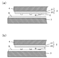
近年、図8(a)にようにウェハ基盤Wに密に形成されダイシングされたチップ部品Cを、所定の間隔を開けて配線基板Sに再配列し、高速高精度に実装する(図8(c))用途がある。例えば、画像表示装置として注目されているマイクロLEDディスプレイ製造においては、数百万個のLEDチップを、間隔を開けTFT基板の所定位置に実装する必要がある。 In recent years, the chip component C densely formed and diced on the wafer substrate W as shown in FIG. 8A is rearranged on the wiring board S at a predetermined interval and mounted at high speed and with high accuracy (FIG. 8A). c)) There are uses. For example, in the manufacture of micro LED displays, which are attracting attention as image display devices, it is necessary to mount millions of LED chips at predetermined positions on a TFT substrate at intervals.
なお、ウェハ基板Wの断面を示す図8(b)および配線基板Sの断面を示す図8(d)の拡大図を図9(a)および図9(b)に示すが、チップ部品Cのバンプ電極Bを配線基板Sの電極(図示せず)が確実に接合するために、誤差数μm程度の精度が必要となる。 Although the enlarged views of FIG. 8B showing the cross section of the wafer substrate W and FIG. 8D showing the cross section of the wiring board S are shown in FIGS. 9A and 9B, the chip component C is shown. In order to reliably join the bump electrode B to the electrode (not shown) of the wiring board S, an accuracy of about several μm is required.
そこで、図8(a)のようにウェハ基板W上に密に形成されたチップ部品Cを、図8(c)のように配線基板Sに所定の間隔を空け(図8(c))、高精度に実装するプロセスが種々検討されている。 Therefore, the chip components C densely formed on the wafer substrate W as shown in FIG. 8 (a) are spaced apart from the wiring board S as shown in FIG. 8 (c) at predetermined intervals (FIG. 8 (c)). Various processes for mounting with high accuracy are being studied.
なかでも、レーザーリフトオフ法(以後LLO法と記す)については多くの検討がなされている(例えば特許文献1)。 In particular, the laser lift-off method (hereinafter referred to as the LLO method) has been studied a lot (for example, Patent Document 1).
図10ではLLO法によりウェハ基板Wから配線基板Sにチップ部品Cを転写配置する例を示している。図10(a)は左端のチップ部品Cにレーザー光Lを照射して、配線基板Sに転写する状態を示している。ここで、左端のチップ部品Cは配線基板Sの所定位置上部に位置合わせされている。また、図10(a)におけるレーザー光Lの波長はチップ部品CをウェハWから剥離するのに適した範囲から選ばれる。例えば、チップ部品Cの素材に吸収される波長を用いれば、温度上昇に伴い素材が分解して生じたガスによりウェハ基板Wからチップ部品Cは剥離される。 FIG. 10 shows an example in which the chip component C is transferred and arranged from the wafer substrate W to the wiring substrate S by the LLO method. FIG. 10A shows a state in which the leftmost chip component C is irradiated with the laser beam L and transferred to the wiring board S. Here, the leftmost chip component C is aligned with the upper portion of the wiring board S at a predetermined position. Further, the wavelength of the laser beam L in FIG. 10A is selected from a range suitable for peeling the chip component C from the wafer W. For example, if a wavelength absorbed by the material of the chip component C is used, the chip component C is peeled from the wafer substrate W by the gas generated by the decomposition of the material as the temperature rises.
図10(b)は、レーザー光Lの照射によりウェハ基板Wから剥離した左端のチップ部品Cが配線基板Sに転写された状態を示している。ここで、左端のチップ部品Cは直下に転写されるため、配線基板Sの所定位置に配置される。なお、転写に伴うチップ部品の直下への移動距離dを、チップ部品CとバンプBの高さの合計より大きくしておけば、配線基板Sにチップ部品Cが転写されていてもウェハ基板Wを水平方向に移動させることは可能である。 FIG. 10B shows a state in which the leftmost chip component C peeled off from the wafer substrate W by irradiation with the laser beam L is transferred to the wiring substrate S. Here, since the leftmost chip component C is transferred directly below, it is arranged at a predetermined position on the wiring board S. If the moving distance d directly below the chip component due to transfer is made larger than the total height of the chip component C and the bump B, the wafer substrate W is transferred even if the chip component C is transferred to the wiring board S. Is possible to move horizontally.
図10(c)は、レーザー光Lの直下に、次に転写すべきチップ部品Cと配線基板Sの所定位置を配置してから、レーザー光Lを照射している状態を示している。このレーザー照射により、先に転写配置したチップ部品Cと間隔を空けて、次のチップ部品Cが配線基板Sの所定位置に転写配置される。 FIG. 10C shows a state in which the laser beam L is irradiated after the predetermined positions of the chip component C to be transferred next and the wiring board S are arranged directly under the laser beam L. By this laser irradiation, the next chip component C is transferred and arranged at a predetermined position on the wiring board S at a distance from the chip component C previously transferred and arranged.
以降も、レーザー光Lの直下に転写すべきチップ部品Cと配線基板Sの所定位置(チップ部品Cを実装すべき位置)を随時配置して、チップ部品Cを転写することにより、図8(c)に示したような配線基板Sへのチップ部品Cの転写配置を行なうことが出来る。 After that, by arranging the chip component C to be transferred and the predetermined position of the wiring board S (the position where the chip component C should be mounted) at any time directly under the laser beam L and transferring the chip component C, FIG. The chip component C can be transferred and arranged on the wiring board S as shown in c).
ところが、図10(a)から図10(b)に示したように、チップ部品Cをウェハ基板Wから剥離するためには、チップ部品Cにはレーザー光Lによる大きなエネルギーが加わる。このため、図10(b)に示した移動距離dの間にもチップ部品Cは加速された状態で配線基板Sに達する。一方、配線基板Sの電極部分は金属であり、加速されたチップ部品Cのバンプ電極Bが金属電極に接する際の衝撃により、図11のようにチップ部品Cが破損することもある。このような衝撃を緩和するために、(封止に用いる未硬化の)熱硬化性接着剤をチップ部品Cのバンプあるいは配線基板Cの電極に被覆しておくことも考えられるが、被覆厚みは5μm以下であり衝撃を緩和するには不充分である。 However, as shown in FIGS. 10A to 10B, in order to separate the chip component C from the wafer substrate W, a large amount of energy due to the laser beam L is applied to the chip component C. Therefore, the chip component C reaches the wiring board S in an accelerated state even during the moving distance d shown in FIG. 10B. On the other hand, the electrode portion of the wiring board S is made of metal, and the chip component C may be damaged as shown in FIG. 11 due to the impact when the bump electrode B of the accelerated chip component C comes into contact with the metal electrode. In order to alleviate such an impact, it is conceivable to coat the bump of the chip component C or the electrode of the wiring board C with a thermosetting adhesive (uncured used for sealing), but the coating thickness is high. It is 5 μm or less, which is insufficient to alleviate the impact.
以上のように、ウェハ基板Wから配線基板Sへの直接転写ではチップ部品Cに加わる衝撃が大きいことから、別に転写基板を用いる転写方式が一般化している。 As described above, since the impact applied to the chip component C is large in the direct transfer from the wafer substrate W to the wiring substrate S, a transfer method using a transfer substrate is generally used.
転写基板を用いる転写方式では、まず、図12(a)に示すように、ウェハ基板Wのチップ部品Cに第1転写基板1を密着させて、レーザー光等によりチップ部品Cを剥離して第1転写基板1に転写する。なお、第1転写基板1はチップ部品Cを保持する側に接着性を有している。ここで、チップ部品Cは第1転写基板と密着した状態で転写するため、加速されることなく、第1転写基板1に転写される。
In the transfer method using a transfer substrate, first, as shown in FIG. 12A, the
ところで、図12(b)に示すように、第1転写基板1ではチップ部品CのバンプBが密着しているため、この状態から配線基板Sにチップ部品Cを転写しても、バンプBを配線基板Sの電極と接触させることはできない。そこで、図12(c)のように、第1転写基板1のチップ部品Cを第2転写基板2に再度転写している。なお、第2転写基板2はチップ部品Cを保持する側に接着性を有している。
By the way, as shown in FIG. 12B, since the bump B of the chip component C is in close contact with the
以上の工程を経て、図12(d)のように、第2転写基板2がチップ部品CのバンプBと反対側を保持することになる。ここで、第2転写基板2とチップ部品Cの接着性を調整することで、図12(d)のようにチップ部品Cを保持した転写基板2を図10のウェハ基板Wの代わりとすることで、転写時のチップ部品Cの衝撃が緩和できる。
Through the above steps, as shown in FIG. 12D, the
しかし、全てのチップ部品Cと第2転写基板2の接着力を一定に管理することは困難であり、一方で、全てのチップ部品を確実に第2転写基板2から剥離するようにレーザー光Lの強度を設定する必要がある。このため、全てのチップ部品Cを破損することなく第2転写基板2から配線基板Sに転写することは極めて困難である。仮に、レーザー光Lが低強度でも剥離可能な接着力にしようとした場合においては、第2転写基板2からチップ部品Cが自然剥離することや、転写時に位置ズレを生じる懸念がある。
However, it is difficult to control the adhesive strength between all the chip parts C and the
本発明は、上記問題を鑑みてなされたものであり、密な状態に配置されたチップ部品を、所定の間隔を空けて配線基板上に実装するのに際して、チップ部品が破損することなく所定の位置に確実に実装するために用いる転写基板ならびに転写基板ならびにこれを用いた実装方法および画像表示装置の製造方法を提供するものである。 The present invention has been made in view of the above problems, and when the chip components arranged in a dense state are mounted on the wiring board at a predetermined interval, the chip components are not damaged and are predetermined. It provides a transfer substrate and a transfer substrate used for reliably mounting at a position, a mounting method using the transfer substrate, and a method for manufacturing an image display device.
上記の課題を解決するために、請求項1に記載の発明は、バンプ電極を有する複数のチップ部品を、前記バンプ電極が形成された面の反対側から保持して、前記バンプ電極と接続する電極を有する配線基板に転写して実装するのに用いる転写基板であって、ベース基板と、ベース基板上に形成され前記チップ部品を保持する接着層とを備え、前記ベース基板に用いる材料は、ヤング率1GPa以上、軟化温度200℃以上、熱伝導率1W/m・K以上の条件を満たし、前記接着層は融点が200℃以上で、反発式硬度計によって測定したリーブ硬さがベース基板のリーブ硬さの50%以上90%以下である転写基板である。
In order to solve the above problems, the invention according to
請求項2に記載の発明は、請求項1に記載の転写基板であって、前記接着層としてシリコーン樹脂またはアクリル樹脂を用いる転写基板である。
The invention according to
請求項3に記載の発明は、ダイシングされたバンプ電極を有するチップ部品を、前記バンプ電極側を保持する第1転写基板に転写し、前記バンプ電極の反対側を保持する第2転写基板に転写してから、前記バンプ電極と接続する電極を有する配線基板に転写して実装する実装方法であって、前記第2転写基板として請求項1または請求項2に記載の転写基板を用い、前記チップ部品を前記第1転写基板から前記第2転写基板に転写する段階で、前記チップ部品の間隔を、前記配線基板への実装間隔に変更し、前記第2転写基板の前記チップ部品を保持した面と反対側から加圧しながら加熱してから、前記転写基板を前記チップ部品から剥離する実装方法である。
The invention according to claim 3 transfers a chip component having a die-dipped bump electrode to a first transfer board holding the bump electrode side, and transfers the chip component to a second transfer board holding the opposite side of the bump electrode. Then, it is a mounting method of transferring and mounting on a wiring board having an electrode to be connected to the bump electrode, wherein the transfer substrate according to
請求項4に記載の発明は、前記チップ部品としてLEDチップを、前記配線基板としてTFT基板を用いて、請求項3に記載の実装方法を用いて画像表示装置を製造する、画像表示装置の製造方法である。
The invention according to
本発明の転写基板を用いた実装を行なうことにより、密な状態に配置されたチップ部品を、所定の間隔を空けて配線基板上に確実に実装することが出来、この転写基板ならびに実装方法でLEDチップをTFT基板に実装することにより高品質な画像表示装置が得られる。 By mounting using the transfer board of the present invention, chip components arranged in a dense state can be reliably mounted on a wiring board at predetermined intervals, and this transfer board and mounting method can be used. By mounting the LED chip on the TFT substrate, a high-quality image display device can be obtained.
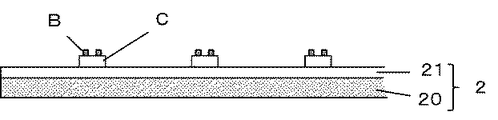
本発明の実施形態について図面を用いて説明する。図1は本発明の実施形態に係る転写基板である第2転写基板2であり、チップ部品Cを保持した状態を示している。
An embodiment of the present invention will be described with reference to the drawings. FIG. 1 is a
図1に示すように第2転写基板2はベース基板20に接着層21が積層され、接着層21がチップ部品CのバンプBとは反対の面を保持する構成となっている。
As shown in FIG. 1, the
ベース基板20は第2転写基板2の機械的、熱的な特性を支配するものであり、寸法安定性に優れ、耐熱性を有しつつ熱伝導率の高いものが望ましい。具体的には、軟化温度が200℃以上で、ヤング率が1GPa以上かつ熱伝導率1W/m・K以上の条件を満たすものが望ましい。この条件を満たすものであれば、ガラス、金属、セラミック、あるいは樹脂であってもよく、透光性は必要としない。
The
接着層21はチップ部品Cを保持するものであるが、第1転写基板1からチップ部品Cを転写される工程(詳しくは後述)の衝撃を緩和するためにベース基板20より柔軟な材質を用いる。柔軟性の指標としては、反発式硬度計によって求めたリーブ硬さが、ベース基板20の50%以上90%以下であることが好ましい。また、融点が200℃以上であることが望ましい。具体的な主成分としては、シリコーン樹脂やアクリル樹脂から選ぶことが出来る。
The
以下、ウェハ基板W上のチップ部品を、配線基板Sに所定の間隔を空けて実装するまでの工程に、図1に示す構成の第2転写基板2を用いた実施形態を図2から図5を用いて説明する。
Hereinafter, embodiments in which the
図2(a)および図2(b)は、ウェハ基板W上のチップ部品Cを第1転写基板1に転写する工程を説明するものであるが、図12(a)および図12(b)に示した従来技術と変わらない。ここで、チップ部品Cは、1辺1mm以下の大きさにダイシングされたものである。本実施形態の説明においては、GaN系のLEDチップを想定しているがSi等の材質からなる半導体集積回路チップ(ICチップ)であってもよい。
2 (a) and 2 (b) explain the process of transferring the chip component C on the wafer substrate W to the
GaN系のLEDにおいては、サファイヤ基板上に積層されたGaN層にLEDチップが形成されている。このため、ウェハ基板Wのチップ部品Cが形成されていない側からレーザーで光エネルギーを照射することにより、光を吸収して過熱したGaN層が分解して窒素ガスを発生して、サファイヤ基板との界面でGaN層が剥離する。この際、第1転写基板1とチップ部品Cは密着しているため、第1転写基板1を固定しておけばチップ部品Cに衝撃力が加わることはない。
In a GaN-based LED, an LED chip is formed on a GaN layer laminated on a sapphire substrate. Therefore, by irradiating light energy with a laser from the side of the wafer substrate W where the chip component C is not formed, the GaN layer that has absorbed the light and overheated is decomposed to generate nitrogen gas, and the sapphire substrate and the sapphire substrate are formed. The GaN layer is peeled off at the interface of. At this time, since the
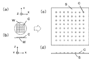
なお、ウェハ基板Wから第1転写基板1へのチップ部品Cする際の上面図を図7(a)に示すが、チップ部品Cの間隔は変わらずに密な状態を維持している。
A top view of the chip component C from the wafer substrate W to the
この後、第1転写基板1から第2転写基板2にチップ部品Cを転写する工程を、図3を用いて説明する。ところで、図12(c)に示した例と異なり、本発明の特徴は、第1転写基板1から第2転写基板2へ転写する段階で、チップ部品Cの間隔を広げ、配線基板Sに実装するときと同じにすることである。この、第1転写基板1と第2転写基板へのチップ部品Cの配置の違いを上面図で示すと図7(b)のようになる。ここで、第2転写基板2へのチップ部品Cの間隔は配線基板Sと同じであり、第2転写基板2のチップ部品Cを配線基板Sの電極側と対向させると全てのチップ部品を同時に配線基板Sの所定位置に位置合わせすることが出来る。
After that, the step of transferring the chip component C from the
図3(a)は、第1転写基板1のチップ部品Cが配置された面と、第2転写基板2の接着層21を、間隔を空けて対向させた状態から、左端のチップ部品Cにレーザー光を照射して、第2転写基板2に転写する状態を示している。ここで、第1転写基板1上のチップ部品C(の非バンプ面)と接着層21の間隔は、バンプBを含むチップ部品Cの高さより大きくしておく必要がある。これは、第1転写基板1と第2転写基板2でチップ部品Cの間隔を変更するため、第1転写基板1と第2転写基板2を対向配置した状態で、面方向に相対位置を変更する必要があるためである。
FIG. 3A shows a state in which the surface on which the chip component C of the
図3(a)において、レーザー光Lは、チップ部品Cのバンプ面側を加熱して第2転写基板2から放出させるものであり、チップ部品Cを構成するGaNに吸収される波長が好ましい。ただし、第1転写基板1のチップ部品Cとの接着層として、光を吸収してガスを放出する材質が使用できるのであれば、レーザー光の波長を接着層の素材に応じて選んでもよい。
In FIG. 3A, the laser beam L heats the bump surface side of the chip component C and emits it from the
図3(b)は、レーザー光Lを照射されたチップ部品Cが、第1転写基板1から放出され第2転写基板2に保持された状態を示している。ここで、チップ部品Cは、僅かな間隔ではあるが、第1転写基板1と第2転写基板2の空間を加速されて、第2転写基板2に到着するこのため、第2転写基板2の接着層21はチップ部品Cが到着した際の衝撃を緩和する必要がある。そこで、チップ部品Cが第2転写基板2に到着した際に破損しない条件を探索した結果、前述のとおり、反発式硬度計によって求めたリーブ硬さが、ベース基板20の50%以上90%以下であるという条件を見出した。この値が90%を超える場合は、チップ部品が破損することがある。一方、50%未満についてはチップ部品が破損することはないが、後工程で加熱する際に粘性等により不都合を生じることがある。
FIG. 3B shows a state in which the chip component C irradiated with the laser beam L is emitted from the
図3(c)は、レーザー光の直下に次に転写すべきチップ部品Cと第2転写基板2の所定位置(先に転写したチップ部品Cと所定間隔)を配置するよう、第1転写基板1と第2転写基板2の相対位置を調整してから、レーザー光Lを照射している状態を示している。このレーザー照射により、先に転写配置したチップ部品Cと所定間隔を空けて、次のチップ部品Cが第2転写基板2に転写配置される(図3(d))。
In FIG. 3C, the first transfer substrate is arranged so that the chip component C to be transferred next and the predetermined position of the second transfer substrate 2 (predetermined distance from the chip component C transferred earlier) are arranged directly under the laser beam. It shows a state in which the laser beam L is irradiated after adjusting the relative positions of the first and the
以降も、レーザー光Lの直下に転写すべきチップ部品Cと第2転写基板2の所定位置(を随時配置して、チップ部品Cを転写することにより、図1に示したような、チップ部品Cを転写配置した第2転写基板2にチップ部品Cを得ることが出来る。
After that, the chip component C to be transferred directly under the laser beam L and the predetermined position of the second transfer substrate 2 (by arranging them at any time to transfer the chip component C, as shown in FIG. 1) The chip component C can be obtained on the
この第2転写基板2を用いて、配線基板Sにチップ部品Cを実装する様子を図4および図5を用いて説明する。
A state in which the chip component C is mounted on the wiring board S using the
図4(a)はステージ3上に配置した配線基板S上のチップ実装位置と、チップ部品Cを位置合わせした状態で第2転写基板2を配置した状態を示している。ここで、第2転写基板2でのチップ部品配置と配線基板Sのチップ部品実装位置は、図7(c)に上面図を示すとおりであり、第2転写基板2に配置された全てのチップ部品を同時に、配線基板Sの実装位置と位置合わせすることができる。
FIG. 4A shows a state in which the
この状態から、第2転写基板2のベース基板20側から熱圧着ヘッド4を接近させ、図4(b)のように加熱圧着することにより、チップ部品Cを配線基板Sの電極と電気的にも機械的にも接合して実装することができる。また、チップ部品Cと配線基板Sの間に予め熱硬化性接着剤を配置しておけば、チップ部品Cの樹脂封止も同時に行なうことができる。
From this state, the
なお、加熱圧着はステージ3と熱圧着ヘッド4の間に挟みこんで行なうため、ステージ3が加熱機能を有していてもよい。
Since the thermocompression bonding is performed by sandwiching it between the
また、加熱圧着において、第2転写基板2が熱変形するとチップ部品Cの実装精度を低下させる。このため、第2転写基板2を構成するベース基板20には、軟化温度が200℃以上で、ヤング率が1GPa以上かつ熱伝導率1W/m・K以上という条件が求められている。また、接着層21については、加熱圧着時に融着することは避けなければならないため、融点200℃以上という条件が求められている。
Further, in the heat crimping, when the
図5(c)は、図4(b)の加熱圧着が完了した後の状態であり、熱圧着ヘッド4を上昇させたものであり、この後、チップ部品Cから第2転写基板を剥離した状態を示したのが図5(d)である。
FIG. 5C shows a state after the heat crimping of FIG. 4B is completed, in which the
図4および図5においては、配線基板S上に第2転写基板2を配置してから、熱圧着ヘッド4を降下させて加熱圧着する例について説明したが、本実施形態の変形例として、熱圧着ヘッド4が第2転写基板2を吸着保持する例を示したのが図6である。図6(a)は熱圧着ヘッド4が第2転写基板2を吸着保持した状態で、配線基板Sとの位置合わせを行っている状態を示しており、図6(b)では熱圧着完了後に熱圧着ヘッド4を上昇することで、チップ部品Cから第2転写基板2の剥離も同時に行なえることを示している。
In FIGS. 4 and 5, an example in which the
以上のように、本発明においては、第2転写基板2から配線基板Sへのチップ部品Cの転写をLLO法で行なうのではなく、加熱圧着により転写と実装を同時に行なうものである。このため、第2転写基板2からチップ部品Cを配線基板Sに写すのに際して、チップ部品Cに衝撃を与えることがない、このため配線基板Sの素材や電極が硬いものであってもチップ部品Cが破損することが防げる。また、第1転写基板1から第2転写基板2へのチップ部品Cの転写にはLLO法を用いているが、第2転写基板2を構成する接着層を適切に選定することにより、第2転写基板2への転写時の衝撃を緩和してチップ部品Cの破損を防ぐことができる。
As described above, in the present invention, the transfer of the chip component C from the
このため、多数のチップ部品を、間隔を空けて実装するような用途において、工程内のチップ破損率を極めて低く抑えることができ、リペアに要するコストも大幅に低減することができる。したがって、配線基板としてTFT基板を用い、チップ部品としてLEDチップを用いるような画像表示装置の製造方法として本発明は好適であり、数百万個のLEDを用いる高品質の画像表示装置の製造方法として極めて適したものである。 Therefore, in an application in which a large number of chip parts are mounted at intervals, the chip breakage rate in the process can be suppressed to an extremely low level, and the cost required for repair can be significantly reduced. Therefore, the present invention is suitable as a method for manufacturing an image display device in which a TFT substrate is used as a wiring board and an LED chip is used as a chip component, and a method for manufacturing a high-quality image display device using millions of LEDs. It is extremely suitable as.
1 第1転写基板
2 第2転写基板
3 ステージ
4 熱圧着ヘッド
20 ベース基板
21 接着層
B バンプ
C チップ部品
L レーザー光
S 配線基板
W ウェハ基板
1
Claims (4)
ベース基板と、ベース基板上に形成され前記チップ部品を保持する接着層とを備え、
前記ベース基板に用いる材料は、ヤング率1GPa以上、軟化温度200℃以上、熱伝導率1W/m・K以上の条件を満たし、
前記接着層は融点が200℃以上で、反発式硬度計によって測定したリーブ硬さがベース基板のリーブ硬さの50%以上90%以下である転写基板。 A transfer substrate used for holding a plurality of chip components having bump electrodes from the opposite side of the surface on which the bump electrodes are formed and transferring them to a wiring board having electrodes connected to the bump electrodes. hand,
A base substrate and an adhesive layer formed on the base substrate to hold the chip components are provided.
The material used for the base substrate satisfies the conditions of Young's modulus of 1 GPa or more, softening temperature of 200 ° C. or more, and thermal conductivity of 1 W / m · K or more.
The adhesive layer is a transfer substrate having a melting point of 200 ° C. or higher and a leave hardness measured by a repulsive hardness tester of 50% or more and 90% or less of the leave hardness of the base substrate.
前記接着層としてシリコーン樹脂またはアクリル樹脂を用いる転写基板。 The transfer substrate according to claim 1.
A transfer substrate using a silicone resin or an acrylic resin as the adhesive layer.
前記第2転写基板として請求項1または請求項2に記載の転写基板を用い、
前記チップ部品を前記第1転写基板から前記第2転写基板に転写する段階で、前記チップ部品の間隔を、前記配線基板への実装間隔に変更し、
前記第2転写基板の前記チップ部品を保持した面と反対側から加圧しながら加熱してから、前記転写基板を前記チップ部品から剥離する実装方法。 A chip component having a diced bump electrode is transferred to a first transfer board holding the bump electrode side, transferred to a second transfer board holding the opposite side of the bump electrode, and then connected to the bump electrode. It is a mounting method that transfers and mounts on a wiring board that has electrodes to be used.
The transfer substrate according to claim 1 or 2 is used as the second transfer substrate.
At the stage of transferring the chip component from the first transfer board to the second transfer board, the interval of the chip component is changed to the mounting interval on the wiring board.
A mounting method in which the transfer substrate is peeled off from the chip component after heating while pressurizing from the side opposite to the surface holding the chip component of the second transfer substrate.
請求項3に記載の実装方法を用いて画像表示装置を製造する、画像表示装置の製造方法 Using an LED chip as the chip component and a TFT substrate as the wiring board,
A method for manufacturing an image display device, which manufactures an image display device using the mounting method according to claim 3.
Priority Applications (3)
| Application Number | Priority Date | Filing Date | Title |
|---|---|---|---|
| JP2018061743A JP6926018B2 (en) | 2018-03-28 | 2018-03-28 | Transfer substrate, mounting method using it, and manufacturing method of image display device |
| PCT/JP2019/009222 WO2019188105A1 (en) | 2018-03-28 | 2019-03-08 | Transfer substrate, mounting method using same, and method for manufacturing image display device |
| TW108110276A TWI758594B (en) | 2018-03-28 | 2019-03-25 | Transfer substrate, mounting method using the same, and manufacturing method of image display device |
Applications Claiming Priority (1)
| Application Number | Priority Date | Filing Date | Title |
|---|---|---|---|
| JP2018061743A JP6926018B2 (en) | 2018-03-28 | 2018-03-28 | Transfer substrate, mounting method using it, and manufacturing method of image display device |
Publications (3)
| Publication Number | Publication Date |
|---|---|
| JP2019175978A JP2019175978A (en) | 2019-10-10 |
| JP2019175978A5 JP2019175978A5 (en) | 2021-02-04 |
| JP6926018B2 true JP6926018B2 (en) | 2021-08-25 |
Family
ID=68059895
Family Applications (1)
| Application Number | Title | Priority Date | Filing Date |
|---|---|---|---|
| JP2018061743A Active JP6926018B2 (en) | 2018-03-28 | 2018-03-28 | Transfer substrate, mounting method using it, and manufacturing method of image display device |
Country Status (3)
| Country | Link |
|---|---|
| JP (1) | JP6926018B2 (en) |
| TW (1) | TWI758594B (en) |
| WO (1) | WO2019188105A1 (en) |
Families Citing this family (3)
| Publication number | Priority date | Publication date | Assignee | Title |
|---|---|---|---|---|
| KR20220158219A (en) * | 2020-03-23 | 2022-11-30 | 토레 엔지니어링 가부시키가이샤 | Mounting method, mounting device, and transfer device |
| JP7463153B2 (en) * | 2020-03-23 | 2024-04-08 | 東レエンジニアリング株式会社 | Mounting method and mounting device |
| TWI744181B (en) * | 2021-01-28 | 2021-10-21 | 台灣愛司帝科技股份有限公司 | Chip-transferring module, and device and method for transferring and bonding chips |
Family Cites Families (10)
| Publication number | Priority date | Publication date | Assignee | Title |
|---|---|---|---|---|
| JP2008130861A (en) * | 2006-11-22 | 2008-06-05 | Sony Corp | Silicon rubber layer laminate and its manufacturing method, abutting device, mounting method of article onto mounting substrate as well as manufacturing method of light emitting diode display device |
| TWI590498B (en) * | 2013-06-03 | 2017-07-01 | 財團法人工業技術研究院 | Electronic device array and method of transfer-bonding electronic devices |
| JP6002334B2 (en) * | 2013-11-05 | 2016-10-05 | 千住金属工業株式会社 | Solder transfer sheet |
| JP2015130476A (en) * | 2013-12-04 | 2015-07-16 | 日東電工株式会社 | Epoxy resin composition for optical semiconductor device and lead frame for optical semiconductor device obtained by using the same, sealed optical semiconductor element and optical semiconductor device |
| JP6446951B2 (en) * | 2014-09-26 | 2019-01-09 | 日亜化学工業株式会社 | Device mounting method and light emitting device manufacturing method |
| WO2016088859A1 (en) * | 2014-12-05 | 2016-06-09 | 日立化成株式会社 | Semiconductor adhesive, and semiconductor device and method for manufacturing same |
| JP2016167544A (en) * | 2015-03-10 | 2016-09-15 | ソニー株式会社 | Electronic component, electronic component mounting board and mounting method of electronic component |
| KR102064584B1 (en) * | 2015-10-29 | 2020-01-10 | 히타치가세이가부시끼가이샤 | Adhesives for semiconductors, semiconductor devices and methods of manufacturing the same |
| US11186757B2 (en) * | 2016-02-08 | 2021-11-30 | Toray Industries, Inc. | Resin composition, resin layer, permanent adhesive, adhesive for temporary bonding, laminated film, processed wafer, and method for manufacturing electronic component or semiconductor device |
| WO2017195517A1 (en) * | 2016-05-09 | 2017-11-16 | 日立化成株式会社 | Method for manufacturing semiconductor device |
-
2018
- 2018-03-28 JP JP2018061743A patent/JP6926018B2/en active Active
-
2019
- 2019-03-08 WO PCT/JP2019/009222 patent/WO2019188105A1/en active Application Filing
- 2019-03-25 TW TW108110276A patent/TWI758594B/en active
Also Published As
| Publication number | Publication date |
|---|---|
| JP2019175978A (en) | 2019-10-10 |
| TWI758594B (en) | 2022-03-21 |
| TW202004933A (en) | 2020-01-16 |
| WO2019188105A1 (en) | 2019-10-03 |
Similar Documents
| Publication | Publication Date | Title |
|---|---|---|
| EP3823030B1 (en) | Method for manufacturing a micro-led display | |
| CN109103116B (en) | Apparatus and method for laser bonding of flip chips | |
| CN109103117B (en) | Apparatus for bonding semiconductor chips and method of bonding semiconductor chips | |
| US10319891B2 (en) | Light emitting module and light emitting module manufacturing method | |
| JP6926018B2 (en) | Transfer substrate, mounting method using it, and manufacturing method of image display device | |
| CN109935664B (en) | Photoelectric semiconductor stamp, method for manufacturing same, and photoelectric semiconductor device | |
| JP2019015899A (en) | Display device manufacturing method, chip component transferring method, and transferring member | |
| JP3959988B2 (en) | Element transfer method | |
| JP7252032B2 (en) | Transfer substrate, mounting method using same, and method for manufacturing image display device | |
| US11538785B2 (en) | Method of using optoelectronic semiconductor stamp to manufacture optoelectronic semiconductor device | |
| JP4745073B2 (en) | Manufacturing method of surface mounted light emitting device | |
| JP5532744B2 (en) | Multi-chip module and method for manufacturing multi-chip module | |
| US10290785B2 (en) | Laminating structure of electronic device using transferring element, transferring apparatus for fabricating the electronic device and method for fabricating the electronic device | |
| KR20160108196A (en) | Method for manufacturing semiconductor device | |
| JP7257187B2 (en) | Chip transfer plate, chip transfer method, image display device manufacturing method, and semiconductor device manufacturing method | |
| JP7335085B2 (en) | Transfer substrate, mounting method using same, and method for manufacturing image display device | |
| JP2012054270A (en) | Method of manufacturing light-emitting device | |
| KR102221588B1 (en) | Apparatus for Bonding Semiconductor Chip and Method for Bonding Semiconductor Chip | |
| US20150249191A1 (en) | Method of manufacturing light-emitting device and wiring substrate for light-emitting element | |
| JP2019523560A (en) | Light emitting device and manufacturing method thereof | |
| WO2019123901A1 (en) | Mounting method and mounting device | |
| KR102547027B1 (en) | Method of bonding a die on a base substrate | |
| US20230134799A1 (en) | Method for manufacturing light-emitting device | |
| KR102573092B1 (en) | Method of bonding a die | |
| KR20200137247A (en) | Micro led display and manufacturing method thereof |
Legal Events
| Date | Code | Title | Description |
|---|---|---|---|
| A621 | Written request for application examination |
Free format text: JAPANESE INTERMEDIATE CODE: A621 Effective date: 20201028 |
|
| A521 | Request for written amendment filed |
Free format text: JAPANESE INTERMEDIATE CODE: A523 Effective date: 20201221 |
|
| TRDD | Decision of grant or rejection written | ||
| A01 | Written decision to grant a patent or to grant a registration (utility model) |
Free format text: JAPANESE INTERMEDIATE CODE: A01 Effective date: 20210720 |
|
| A61 | First payment of annual fees (during grant procedure) |
Free format text: JAPANESE INTERMEDIATE CODE: A61 Effective date: 20210804 |
|
| R150 | Certificate of patent or registration of utility model |
Ref document number: 6926018 Country of ref document: JP Free format text: JAPANESE INTERMEDIATE CODE: R150 |