JP6916426B2 - Laminated structure and its manufacturing method, semiconductor device and crystal film - Google Patents
Laminated structure and its manufacturing method, semiconductor device and crystal film Download PDFInfo
- Publication number
- JP6916426B2 JP6916426B2 JP2016546608A JP2016546608A JP6916426B2 JP 6916426 B2 JP6916426 B2 JP 6916426B2 JP 2016546608 A JP2016546608 A JP 2016546608A JP 2016546608 A JP2016546608 A JP 2016546608A JP 6916426 B2 JP6916426 B2 JP 6916426B2
- Authority
- JP
- Japan
- Prior art keywords
- film
- crystal
- type semiconductor
- crystal film
- semiconductor layer
- Prior art date
- Legal status (The legal status is an assumption and is not a legal conclusion. Google has not performed a legal analysis and makes no representation as to the accuracy of the status listed.)
- Active
Links
- 239000013078 crystal Substances 0.000 title claims description 221
- 239000004065 semiconductor Substances 0.000 title claims description 210
- 238000004519 manufacturing process Methods 0.000 title description 12
- 229910052593 corundum Inorganic materials 0.000 claims description 27
- 239000010431 corundum Substances 0.000 claims description 27
- 239000002019 doping agent Substances 0.000 claims description 27
- 229910052751 metal Inorganic materials 0.000 claims description 23
- 239000002184 metal Substances 0.000 claims description 22
- GYHNNYVSQQEPJS-UHFFFAOYSA-N Gallium Chemical compound [Ga] GYHNNYVSQQEPJS-UHFFFAOYSA-N 0.000 claims description 21
- 229910052733 gallium Inorganic materials 0.000 claims description 21
- 239000010408 film Substances 0.000 description 224
- 239000010410 layer Substances 0.000 description 207
- 239000000758 substrate Substances 0.000 description 123
- 239000003595 mist Substances 0.000 description 41
- 239000002994 raw material Substances 0.000 description 36
- 239000012212 insulator Substances 0.000 description 31
- 238000000034 method Methods 0.000 description 30
- 229910052594 sapphire Inorganic materials 0.000 description 28
- 239000010980 sapphire Substances 0.000 description 28
- 239000000243 solution Substances 0.000 description 24
- 239000012159 carrier gas Substances 0.000 description 23
- 229910052738 indium Inorganic materials 0.000 description 21
- 230000015572 biosynthetic process Effects 0.000 description 20
- 239000010409 thin film Substances 0.000 description 19
- 229910052782 aluminium Inorganic materials 0.000 description 18
- XLOMVQKBTHCTTD-UHFFFAOYSA-N Zinc monoxide Chemical compound [Zn]=O XLOMVQKBTHCTTD-UHFFFAOYSA-N 0.000 description 16
- 150000002739 metals Chemical class 0.000 description 15
- 150000001875 compounds Chemical class 0.000 description 14
- 239000007772 electrode material Substances 0.000 description 14
- APFVFJFRJDLVQX-UHFFFAOYSA-N indium atom Chemical compound [In] APFVFJFRJDLVQX-UHFFFAOYSA-N 0.000 description 14
- 230000005355 Hall effect Effects 0.000 description 13
- 229910044991 metal oxide Inorganic materials 0.000 description 13
- 150000004706 metal oxides Chemical class 0.000 description 13
- 229910052718 tin Inorganic materials 0.000 description 13
- 239000011135 tin Substances 0.000 description 13
- 230000005669 field effect Effects 0.000 description 12
- AMGQUBHHOARCQH-UHFFFAOYSA-N indium;oxotin Chemical compound [In].[Sn]=O AMGQUBHHOARCQH-UHFFFAOYSA-N 0.000 description 12
- 239000000203 mixture Substances 0.000 description 12
- 239000010936 titanium Substances 0.000 description 12
- 230000004888 barrier function Effects 0.000 description 11
- 239000000463 material Substances 0.000 description 11
- 238000004544 sputter deposition Methods 0.000 description 11
- 229910052719 titanium Inorganic materials 0.000 description 11
- 230000002159 abnormal effect Effects 0.000 description 10
- XAGFODPZIPBFFR-UHFFFAOYSA-N aluminium Chemical compound [Al] XAGFODPZIPBFFR-UHFFFAOYSA-N 0.000 description 10
- 230000000052 comparative effect Effects 0.000 description 10
- XEEYBQQBJWHFJM-UHFFFAOYSA-N iron Substances [Fe] XEEYBQQBJWHFJM-UHFFFAOYSA-N 0.000 description 10
- 229910052758 niobium Inorganic materials 0.000 description 10
- 239000010955 niobium Substances 0.000 description 10
- 229910052720 vanadium Inorganic materials 0.000 description 10
- 229910052726 zirconium Inorganic materials 0.000 description 10
- 238000005229 chemical vapour deposition Methods 0.000 description 9
- 239000003112 inhibitor Substances 0.000 description 8
- 239000011787 zinc oxide Substances 0.000 description 8
- 229910052779 Neodymium Inorganic materials 0.000 description 7
- 229910045601 alloy Inorganic materials 0.000 description 7
- 239000000956 alloy Substances 0.000 description 7
- 229910052804 chromium Inorganic materials 0.000 description 7
- 239000011651 chromium Substances 0.000 description 7
- 229910052802 copper Inorganic materials 0.000 description 7
- 238000005530 etching Methods 0.000 description 7
- 229910052737 gold Inorganic materials 0.000 description 7
- 229910052735 hafnium Inorganic materials 0.000 description 7
- 229910003437 indium oxide Inorganic materials 0.000 description 7
- PJXISJQVUVHSOJ-UHFFFAOYSA-N indium(iii) oxide Chemical compound [O-2].[O-2].[O-2].[In+3].[In+3] PJXISJQVUVHSOJ-UHFFFAOYSA-N 0.000 description 7
- 229910052741 iridium Inorganic materials 0.000 description 7
- 229910052742 iron Inorganic materials 0.000 description 7
- 229910052748 manganese Inorganic materials 0.000 description 7
- 229910052750 molybdenum Inorganic materials 0.000 description 7
- 229910052759 nickel Inorganic materials 0.000 description 7
- 229910052763 palladium Inorganic materials 0.000 description 7
- 229910052697 platinum Inorganic materials 0.000 description 7
- 229920000767 polyaniline Polymers 0.000 description 7
- 229920000128 polypyrrole Polymers 0.000 description 7
- 229920000123 polythiophene Polymers 0.000 description 7
- 229910052709 silver Inorganic materials 0.000 description 7
- 229910052715 tantalum Inorganic materials 0.000 description 7
- XOLBLPGZBRYERU-UHFFFAOYSA-N tin dioxide Chemical compound O=[Sn]=O XOLBLPGZBRYERU-UHFFFAOYSA-N 0.000 description 7
- 229910001887 tin oxide Inorganic materials 0.000 description 7
- 229910052721 tungsten Inorganic materials 0.000 description 7
- 238000007740 vapor deposition Methods 0.000 description 7
- 229910052725 zinc Inorganic materials 0.000 description 7
- 239000011701 zinc Substances 0.000 description 7
- ATJFFYVFTNAWJD-UHFFFAOYSA-N Tin Chemical compound [Sn] ATJFFYVFTNAWJD-UHFFFAOYSA-N 0.000 description 6
- 238000006243 chemical reaction Methods 0.000 description 6
- OKTJSMMVPCPJKN-UHFFFAOYSA-N Carbon Chemical compound [C] OKTJSMMVPCPJKN-UHFFFAOYSA-N 0.000 description 5
- 238000000137 annealing Methods 0.000 description 5
- 229910052799 carbon Inorganic materials 0.000 description 5
- AJNVQOSZGJRYEI-UHFFFAOYSA-N digallium;oxygen(2-) Chemical compound [O-2].[O-2].[O-2].[Ga+3].[Ga+3] AJNVQOSZGJRYEI-UHFFFAOYSA-N 0.000 description 5
- 239000007789 gas Substances 0.000 description 5
- 229910052732 germanium Inorganic materials 0.000 description 5
- GNPVGFCGXDBREM-UHFFFAOYSA-N germanium atom Chemical compound [Ge] GNPVGFCGXDBREM-UHFFFAOYSA-N 0.000 description 5
- IJGRMHOSHXDMSA-UHFFFAOYSA-N Atomic nitrogen Chemical compound N#N IJGRMHOSHXDMSA-UHFFFAOYSA-N 0.000 description 4
- 229910005191 Ga 2 O 3 Inorganic materials 0.000 description 4
- XUIMIQQOPSSXEZ-UHFFFAOYSA-N Silicon Chemical compound [Si] XUIMIQQOPSSXEZ-UHFFFAOYSA-N 0.000 description 4
- RTAQQCXQSZGOHL-UHFFFAOYSA-N Titanium Chemical compound [Ti] RTAQQCXQSZGOHL-UHFFFAOYSA-N 0.000 description 4
- -1 aluminum compound Chemical class 0.000 description 4
- 238000000089 atomic force micrograph Methods 0.000 description 4
- 229910052792 caesium Inorganic materials 0.000 description 4
- TVFDJXOCXUVLDH-UHFFFAOYSA-N caesium atom Chemical compound [Cs] TVFDJXOCXUVLDH-UHFFFAOYSA-N 0.000 description 4
- 150000002259 gallium compounds Chemical class 0.000 description 4
- 229910001195 gallium oxide Inorganic materials 0.000 description 4
- 150000004820 halides Chemical class 0.000 description 4
- 230000001771 impaired effect Effects 0.000 description 4
- 238000009413 insulation Methods 0.000 description 4
- 239000011777 magnesium Substances 0.000 description 4
- 229910052710 silicon Inorganic materials 0.000 description 4
- 239000010703 silicon Substances 0.000 description 4
- XLYOFNOQVPJJNP-UHFFFAOYSA-N water Substances O XLYOFNOQVPJJNP-UHFFFAOYSA-N 0.000 description 4
- CPELXLSAUQHCOX-UHFFFAOYSA-M Bromide Chemical compound [Br-] CPELXLSAUQHCOX-UHFFFAOYSA-M 0.000 description 3
- KJTLSVCANCCWHF-UHFFFAOYSA-N Ruthenium Chemical compound [Ru] KJTLSVCANCCWHF-UHFFFAOYSA-N 0.000 description 3
- QCWXUUIWCKQGHC-UHFFFAOYSA-N Zirconium Chemical compound [Zr] QCWXUUIWCKQGHC-UHFFFAOYSA-N 0.000 description 3
- 230000001133 acceleration Effects 0.000 description 3
- 239000004020 conductor Substances 0.000 description 3
- 238000000407 epitaxy Methods 0.000 description 3
- 239000010419 fine particle Substances 0.000 description 3
- YBMRDBCBODYGJE-UHFFFAOYSA-N germanium oxide Inorganic materials O=[Ge]=O YBMRDBCBODYGJE-UHFFFAOYSA-N 0.000 description 3
- XMBWDFGMSWQBCA-UHFFFAOYSA-N hydrogen iodide Chemical compound I XMBWDFGMSWQBCA-UHFFFAOYSA-N 0.000 description 3
- 239000012535 impurity Substances 0.000 description 3
- GUCVJGMIXFAOAE-UHFFFAOYSA-N niobium atom Chemical compound [Nb] GUCVJGMIXFAOAE-UHFFFAOYSA-N 0.000 description 3
- PVADDRMAFCOOPC-UHFFFAOYSA-N oxogermanium Chemical compound [Ge]=O PVADDRMAFCOOPC-UHFFFAOYSA-N 0.000 description 3
- 239000010453 quartz Substances 0.000 description 3
- 229910052707 ruthenium Inorganic materials 0.000 description 3
- VYPSYNLAJGMNEJ-UHFFFAOYSA-N silicon dioxide Inorganic materials O=[Si]=O VYPSYNLAJGMNEJ-UHFFFAOYSA-N 0.000 description 3
- 238000001771 vacuum deposition Methods 0.000 description 3
- GPPXJZIENCGNKB-UHFFFAOYSA-N vanadium Chemical compound [V]#[V] GPPXJZIENCGNKB-UHFFFAOYSA-N 0.000 description 3
- BMYNFMYTOJXKLE-UHFFFAOYSA-N 3-azaniumyl-2-hydroxypropanoate Chemical compound NCC(O)C(O)=O BMYNFMYTOJXKLE-UHFFFAOYSA-N 0.000 description 2
- XKRFYHLGVUSROY-UHFFFAOYSA-N Argon Chemical compound [Ar] XKRFYHLGVUSROY-UHFFFAOYSA-N 0.000 description 2
- VEXZGXHMUGYJMC-UHFFFAOYSA-M Chloride anion Chemical compound [Cl-] VEXZGXHMUGYJMC-UHFFFAOYSA-M 0.000 description 2
- MYMOFIZGZYHOMD-UHFFFAOYSA-N Dioxygen Chemical compound O=O MYMOFIZGZYHOMD-UHFFFAOYSA-N 0.000 description 2
- KRHYYFGTRYWZRS-UHFFFAOYSA-M Fluoride anion Chemical compound [F-] KRHYYFGTRYWZRS-UHFFFAOYSA-M 0.000 description 2
- VEXZGXHMUGYJMC-UHFFFAOYSA-N Hydrochloric acid Chemical compound Cl VEXZGXHMUGYJMC-UHFFFAOYSA-N 0.000 description 2
- FYYHWMGAXLPEAU-UHFFFAOYSA-N Magnesium Chemical compound [Mg] FYYHWMGAXLPEAU-UHFFFAOYSA-N 0.000 description 2
- CPLXHLVBOLITMK-UHFFFAOYSA-N Magnesium oxide Chemical compound [Mg]=O CPLXHLVBOLITMK-UHFFFAOYSA-N 0.000 description 2
- 229910052788 barium Inorganic materials 0.000 description 2
- DSAJWYNOEDNPEQ-UHFFFAOYSA-N barium atom Chemical compound [Ba] DSAJWYNOEDNPEQ-UHFFFAOYSA-N 0.000 description 2
- 229910052794 bromium Inorganic materials 0.000 description 2
- 230000006866 deterioration Effects 0.000 description 2
- 238000010586 diagram Methods 0.000 description 2
- 229910001873 dinitrogen Inorganic materials 0.000 description 2
- 229910001882 dioxygen Inorganic materials 0.000 description 2
- 238000007599 discharging Methods 0.000 description 2
- 238000011156 evaluation Methods 0.000 description 2
- SRVXDMYFQIODQI-UHFFFAOYSA-K gallium(iii) bromide Chemical compound Br[Ga](Br)Br SRVXDMYFQIODQI-UHFFFAOYSA-K 0.000 description 2
- 230000006698 induction Effects 0.000 description 2
- 229910052740 iodine Inorganic materials 0.000 description 2
- 229910052749 magnesium Inorganic materials 0.000 description 2
- 238000005259 measurement Methods 0.000 description 2
- 230000003287 optical effect Effects 0.000 description 2
- 230000003647 oxidation Effects 0.000 description 2
- 238000007254 oxidation reaction Methods 0.000 description 2
- 238000005498 polishing Methods 0.000 description 2
- 229910021420 polycrystalline silicon Inorganic materials 0.000 description 2
- 229920005591 polysilicon Polymers 0.000 description 2
- 238000002360 preparation method Methods 0.000 description 2
- 229910052712 strontium Inorganic materials 0.000 description 2
- CIOAGBVUUVVLOB-UHFFFAOYSA-N strontium atom Chemical compound [Sr] CIOAGBVUUVVLOB-UHFFFAOYSA-N 0.000 description 2
- 239000000126 substance Substances 0.000 description 2
- 230000003746 surface roughness Effects 0.000 description 2
- FWPIDFUJEMBDLS-UHFFFAOYSA-L tin(II) chloride dihydrate Chemical compound O.O.Cl[Sn]Cl FWPIDFUJEMBDLS-UHFFFAOYSA-L 0.000 description 2
- 238000011144 upstream manufacturing Methods 0.000 description 2
- YVTHLONGBIQYBO-UHFFFAOYSA-N zinc indium(3+) oxygen(2-) Chemical compound [O--].[Zn++].[In+3] YVTHLONGBIQYBO-UHFFFAOYSA-N 0.000 description 2
- ZVYYAYJIGYODSD-LNTINUHCSA-K (z)-4-bis[[(z)-4-oxopent-2-en-2-yl]oxy]gallanyloxypent-3-en-2-one Chemical compound [Ga+3].C\C([O-])=C\C(C)=O.C\C([O-])=C\C(C)=O.C\C([O-])=C\C(C)=O ZVYYAYJIGYODSD-LNTINUHCSA-K 0.000 description 1
- POILWHVDKZOXJZ-ARJAWSKDSA-M (z)-4-oxopent-2-en-2-olate Chemical compound C\C([O-])=C\C(C)=O POILWHVDKZOXJZ-ARJAWSKDSA-M 0.000 description 1
- 229910018072 Al 2 O 3 Inorganic materials 0.000 description 1
- 229910020203 CeO Inorganic materials 0.000 description 1
- UFHFLCQGNIYNRP-UHFFFAOYSA-N Hydrogen Chemical compound [H][H] UFHFLCQGNIYNRP-UHFFFAOYSA-N 0.000 description 1
- MHAJPDPJQMAIIY-UHFFFAOYSA-N Hydrogen peroxide Chemical compound OO MHAJPDPJQMAIIY-UHFFFAOYSA-N 0.000 description 1
- 229910004541 SiN Inorganic materials 0.000 description 1
- 229910004298 SiO 2 Inorganic materials 0.000 description 1
- 229910006404 SnO 2 Inorganic materials 0.000 description 1
- 229910010413 TiO 2 Inorganic materials 0.000 description 1
- 230000005856 abnormality Effects 0.000 description 1
- 238000010521 absorption reaction Methods 0.000 description 1
- 239000007864 aqueous solution Substances 0.000 description 1
- 229910052786 argon Inorganic materials 0.000 description 1
- QVGXLLKOCUKJST-UHFFFAOYSA-N atomic oxygen Chemical compound [O] QVGXLLKOCUKJST-UHFFFAOYSA-N 0.000 description 1
- 239000006227 byproduct Substances 0.000 description 1
- 229910052801 chlorine Inorganic materials 0.000 description 1
- 238000000576 coating method Methods 0.000 description 1
- 238000007796 conventional method Methods 0.000 description 1
- 150000004696 coordination complex Chemical class 0.000 description 1
- 238000005520 cutting process Methods 0.000 description 1
- 230000000694 effects Effects 0.000 description 1
- 229910052731 fluorine Inorganic materials 0.000 description 1
- 229910052736 halogen Inorganic materials 0.000 description 1
- 150000002367 halogens Chemical class 0.000 description 1
- 150000002472 indium compounds Chemical class 0.000 description 1
- 239000011261 inert gas Substances 0.000 description 1
- 238000007733 ion plating Methods 0.000 description 1
- 150000002500 ions Chemical class 0.000 description 1
- 238000010030 laminating Methods 0.000 description 1
- 229910052757 nitrogen Inorganic materials 0.000 description 1
- 239000003960 organic solvent Substances 0.000 description 1
- 239000001301 oxygen Substances 0.000 description 1
- 229910052760 oxygen Inorganic materials 0.000 description 1
- 239000002245 particle Substances 0.000 description 1
- 230000002093 peripheral effect Effects 0.000 description 1
- 238000000206 photolithography Methods 0.000 description 1
- 230000000704 physical effect Effects 0.000 description 1
- 238000000053 physical method Methods 0.000 description 1
- 238000005268 plasma chemical vapour deposition Methods 0.000 description 1
- 238000001020 plasma etching Methods 0.000 description 1
- 238000012545 processing Methods 0.000 description 1
- 230000000644 propagated effect Effects 0.000 description 1
- 239000011241 protective layer Substances 0.000 description 1
- 229910052814 silicon oxide Inorganic materials 0.000 description 1
- 239000002356 single layer Substances 0.000 description 1
- 239000007787 solid Substances 0.000 description 1
- 239000002904 solvent Substances 0.000 description 1
- 239000007921 spray Substances 0.000 description 1
- 239000007858 starting material Substances 0.000 description 1
- 230000003068 static effect Effects 0.000 description 1
Images


Classifications
-
- H—ELECTRICITY
- H01—ELECTRIC ELEMENTS
- H01L—SEMICONDUCTOR DEVICES NOT COVERED BY CLASS H10
- H01L21/00—Processes or apparatus adapted for the manufacture or treatment of semiconductor or solid state devices or of parts thereof
- H01L21/02—Manufacture or treatment of semiconductor devices or of parts thereof
- H01L21/02104—Forming layers
- H01L21/02365—Forming inorganic semiconducting materials on a substrate
- H01L21/02518—Deposited layers
- H01L21/02521—Materials
- H01L21/02565—Oxide semiconducting materials not being Group 12/16 materials, e.g. ternary compounds
-
- H—ELECTRICITY
- H01—ELECTRIC ELEMENTS
- H01L—SEMICONDUCTOR DEVICES NOT COVERED BY CLASS H10
- H01L21/00—Processes or apparatus adapted for the manufacture or treatment of semiconductor or solid state devices or of parts thereof
- H01L21/02—Manufacture or treatment of semiconductor devices or of parts thereof
- H01L21/02104—Forming layers
- H01L21/02365—Forming inorganic semiconducting materials on a substrate
- H01L21/02367—Substrates
- H01L21/0237—Materials
- H01L21/02414—Oxide semiconducting materials not being Group 12/16 materials, e.g. ternary compounds
-
- H—ELECTRICITY
- H01—ELECTRIC ELEMENTS
- H01L—SEMICONDUCTOR DEVICES NOT COVERED BY CLASS H10
- H01L21/00—Processes or apparatus adapted for the manufacture or treatment of semiconductor or solid state devices or of parts thereof
- H01L21/02—Manufacture or treatment of semiconductor devices or of parts thereof
- H01L21/02104—Forming layers
- H01L21/02365—Forming inorganic semiconducting materials on a substrate
- H01L21/02367—Substrates
- H01L21/02433—Crystal orientation
-
- H—ELECTRICITY
- H01—ELECTRIC ELEMENTS
- H01L—SEMICONDUCTOR DEVICES NOT COVERED BY CLASS H10
- H01L21/00—Processes or apparatus adapted for the manufacture or treatment of semiconductor or solid state devices or of parts thereof
- H01L21/02—Manufacture or treatment of semiconductor devices or of parts thereof
- H01L21/02104—Forming layers
- H01L21/02365—Forming inorganic semiconducting materials on a substrate
- H01L21/02518—Deposited layers
- H01L21/0257—Doping during depositing
- H01L21/02573—Conductivity type
- H01L21/02576—N-type
-
- H—ELECTRICITY
- H01—ELECTRIC ELEMENTS
- H01L—SEMICONDUCTOR DEVICES NOT COVERED BY CLASS H10
- H01L21/00—Processes or apparatus adapted for the manufacture or treatment of semiconductor or solid state devices or of parts thereof
- H01L21/02—Manufacture or treatment of semiconductor devices or of parts thereof
- H01L21/02104—Forming layers
- H01L21/02365—Forming inorganic semiconducting materials on a substrate
- H01L21/02518—Deposited layers
- H01L21/0257—Doping during depositing
- H01L21/02573—Conductivity type
- H01L21/02579—P-type
-
- H—ELECTRICITY
- H01—ELECTRIC ELEMENTS
- H01L—SEMICONDUCTOR DEVICES NOT COVERED BY CLASS H10
- H01L21/00—Processes or apparatus adapted for the manufacture or treatment of semiconductor or solid state devices or of parts thereof
- H01L21/02—Manufacture or treatment of semiconductor devices or of parts thereof
- H01L21/02104—Forming layers
- H01L21/02365—Forming inorganic semiconducting materials on a substrate
- H01L21/02518—Deposited layers
- H01L21/0257—Doping during depositing
- H01L21/02573—Conductivity type
- H01L21/02581—Transition metal or rare earth elements
-
- H—ELECTRICITY
- H01—ELECTRIC ELEMENTS
- H01L—SEMICONDUCTOR DEVICES NOT COVERED BY CLASS H10
- H01L21/00—Processes or apparatus adapted for the manufacture or treatment of semiconductor or solid state devices or of parts thereof
- H01L21/02—Manufacture or treatment of semiconductor devices or of parts thereof
- H01L21/02104—Forming layers
- H01L21/02365—Forming inorganic semiconducting materials on a substrate
- H01L21/02612—Formation types
- H01L21/02617—Deposition types
- H01L21/0262—Reduction or decomposition of gaseous compounds, e.g. CVD
-
- H—ELECTRICITY
- H01—ELECTRIC ELEMENTS
- H01L—SEMICONDUCTOR DEVICES NOT COVERED BY CLASS H10
- H01L21/00—Processes or apparatus adapted for the manufacture or treatment of semiconductor or solid state devices or of parts thereof
- H01L21/02—Manufacture or treatment of semiconductor devices or of parts thereof
- H01L21/02104—Forming layers
- H01L21/02365—Forming inorganic semiconducting materials on a substrate
- H01L21/02612—Formation types
- H01L21/02617—Deposition types
- H01L21/02623—Liquid deposition
- H01L21/02628—Liquid deposition using solutions
-
- H—ELECTRICITY
- H01—ELECTRIC ELEMENTS
- H01L—SEMICONDUCTOR DEVICES NOT COVERED BY CLASS H10
- H01L21/00—Processes or apparatus adapted for the manufacture or treatment of semiconductor or solid state devices or of parts thereof
- H01L21/02—Manufacture or treatment of semiconductor devices or of parts thereof
- H01L21/04—Manufacture or treatment of semiconductor devices or of parts thereof the devices having at least one potential-jump barrier or surface barrier, e.g. PN junction, depletion layer or carrier concentration layer
- H01L21/18—Manufacture or treatment of semiconductor devices or of parts thereof the devices having at least one potential-jump barrier or surface barrier, e.g. PN junction, depletion layer or carrier concentration layer the devices having semiconductor bodies comprising elements of Group IV of the Periodic System or AIIIBV compounds with or without impurities, e.g. doping materials
- H01L21/24—Alloying of impurity materials, e.g. doping materials, electrode materials, with a semiconductor body
- H01L21/242—Alloying of doping materials with AIIIBV compounds
-
- H—ELECTRICITY
- H01—ELECTRIC ELEMENTS
- H01L—SEMICONDUCTOR DEVICES NOT COVERED BY CLASS H10
- H01L29/00—Semiconductor devices adapted for rectifying, amplifying, oscillating or switching, or capacitors or resistors with at least one potential-jump barrier or surface barrier, e.g. PN junction depletion layer or carrier concentration layer; Details of semiconductor bodies or of electrodes thereof ; Multistep manufacturing processes therefor
- H01L29/02—Semiconductor bodies ; Multistep manufacturing processes therefor
- H01L29/04—Semiconductor bodies ; Multistep manufacturing processes therefor characterised by their crystalline structure, e.g. polycrystalline, cubic or particular orientation of crystalline planes
- H01L29/045—Semiconductor bodies ; Multistep manufacturing processes therefor characterised by their crystalline structure, e.g. polycrystalline, cubic or particular orientation of crystalline planes by their particular orientation of crystalline planes
-
- H—ELECTRICITY
- H01—ELECTRIC ELEMENTS
- H01L—SEMICONDUCTOR DEVICES NOT COVERED BY CLASS H10
- H01L29/00—Semiconductor devices adapted for rectifying, amplifying, oscillating or switching, or capacitors or resistors with at least one potential-jump barrier or surface barrier, e.g. PN junction depletion layer or carrier concentration layer; Details of semiconductor bodies or of electrodes thereof ; Multistep manufacturing processes therefor
- H01L29/02—Semiconductor bodies ; Multistep manufacturing processes therefor
- H01L29/12—Semiconductor bodies ; Multistep manufacturing processes therefor characterised by the materials of which they are formed
- H01L29/24—Semiconductor bodies ; Multistep manufacturing processes therefor characterised by the materials of which they are formed including, apart from doping materials or other impurities, only semiconductor materials not provided for in groups H01L29/16, H01L29/18, H01L29/20, H01L29/22
-
- H—ELECTRICITY
- H01—ELECTRIC ELEMENTS
- H01L—SEMICONDUCTOR DEVICES NOT COVERED BY CLASS H10
- H01L29/00—Semiconductor devices adapted for rectifying, amplifying, oscillating or switching, or capacitors or resistors with at least one potential-jump barrier or surface barrier, e.g. PN junction depletion layer or carrier concentration layer; Details of semiconductor bodies or of electrodes thereof ; Multistep manufacturing processes therefor
- H01L29/66—Types of semiconductor device ; Multistep manufacturing processes therefor
- H01L29/66007—Multistep manufacturing processes
- H01L29/66969—Multistep manufacturing processes of devices having semiconductor bodies not comprising group 14 or group 13/15 materials
-
- H—ELECTRICITY
- H01—ELECTRIC ELEMENTS
- H01L—SEMICONDUCTOR DEVICES NOT COVERED BY CLASS H10
- H01L29/00—Semiconductor devices adapted for rectifying, amplifying, oscillating or switching, or capacitors or resistors with at least one potential-jump barrier or surface barrier, e.g. PN junction depletion layer or carrier concentration layer; Details of semiconductor bodies or of electrodes thereof ; Multistep manufacturing processes therefor
- H01L29/66—Types of semiconductor device ; Multistep manufacturing processes therefor
- H01L29/68—Types of semiconductor device ; Multistep manufacturing processes therefor controllable by only the electric current supplied, or only the electric potential applied, to an electrode which does not carry the current to be rectified, amplified or switched
- H01L29/70—Bipolar devices
- H01L29/72—Transistor-type devices, i.e. able to continuously respond to applied control signals
- H01L29/739—Transistor-type devices, i.e. able to continuously respond to applied control signals controlled by field-effect, e.g. bipolar static induction transistors [BSIT]
- H01L29/7393—Insulated gate bipolar mode transistors, i.e. IGBT; IGT; COMFET
- H01L29/7395—Vertical transistors, e.g. vertical IGBT
-
- H—ELECTRICITY
- H01—ELECTRIC ELEMENTS
- H01L—SEMICONDUCTOR DEVICES NOT COVERED BY CLASS H10
- H01L29/00—Semiconductor devices adapted for rectifying, amplifying, oscillating or switching, or capacitors or resistors with at least one potential-jump barrier or surface barrier, e.g. PN junction depletion layer or carrier concentration layer; Details of semiconductor bodies or of electrodes thereof ; Multistep manufacturing processes therefor
- H01L29/66—Types of semiconductor device ; Multistep manufacturing processes therefor
- H01L29/68—Types of semiconductor device ; Multistep manufacturing processes therefor controllable by only the electric current supplied, or only the electric potential applied, to an electrode which does not carry the current to be rectified, amplified or switched
- H01L29/76—Unipolar devices, e.g. field effect transistors
- H01L29/772—Field effect transistors
- H01L29/778—Field effect transistors with two-dimensional charge carrier gas channel, e.g. HEMT ; with two-dimensional charge-carrier layer formed at a heterojunction interface
- H01L29/7786—Field effect transistors with two-dimensional charge carrier gas channel, e.g. HEMT ; with two-dimensional charge-carrier layer formed at a heterojunction interface with direct single heterostructure, i.e. with wide bandgap layer formed on top of active layer, e.g. direct single heterostructure MIS-like HEMT
-
- H—ELECTRICITY
- H01—ELECTRIC ELEMENTS
- H01L—SEMICONDUCTOR DEVICES NOT COVERED BY CLASS H10
- H01L29/00—Semiconductor devices adapted for rectifying, amplifying, oscillating or switching, or capacitors or resistors with at least one potential-jump barrier or surface barrier, e.g. PN junction depletion layer or carrier concentration layer; Details of semiconductor bodies or of electrodes thereof ; Multistep manufacturing processes therefor
- H01L29/66—Types of semiconductor device ; Multistep manufacturing processes therefor
- H01L29/68—Types of semiconductor device ; Multistep manufacturing processes therefor controllable by only the electric current supplied, or only the electric potential applied, to an electrode which does not carry the current to be rectified, amplified or switched
- H01L29/76—Unipolar devices, e.g. field effect transistors
- H01L29/772—Field effect transistors
- H01L29/78—Field effect transistors with field effect produced by an insulated gate
- H01L29/7801—DMOS transistors, i.e. MISFETs with a channel accommodating body or base region adjoining a drain drift region
- H01L29/7802—Vertical DMOS transistors, i.e. VDMOS transistors
- H01L29/7813—Vertical DMOS transistors, i.e. VDMOS transistors with trench gate electrode, e.g. UMOS transistors
-
- H—ELECTRICITY
- H01—ELECTRIC ELEMENTS
- H01L—SEMICONDUCTOR DEVICES NOT COVERED BY CLASS H10
- H01L29/00—Semiconductor devices adapted for rectifying, amplifying, oscillating or switching, or capacitors or resistors with at least one potential-jump barrier or surface barrier, e.g. PN junction depletion layer or carrier concentration layer; Details of semiconductor bodies or of electrodes thereof ; Multistep manufacturing processes therefor
- H01L29/66—Types of semiconductor device ; Multistep manufacturing processes therefor
- H01L29/68—Types of semiconductor device ; Multistep manufacturing processes therefor controllable by only the electric current supplied, or only the electric potential applied, to an electrode which does not carry the current to be rectified, amplified or switched
- H01L29/76—Unipolar devices, e.g. field effect transistors
- H01L29/772—Field effect transistors
- H01L29/78—Field effect transistors with field effect produced by an insulated gate
- H01L29/7827—Vertical transistors
- H01L29/7828—Vertical transistors without inversion channel, e.g. vertical ACCUFETs, normally-on vertical MISFETs
-
- H—ELECTRICITY
- H01—ELECTRIC ELEMENTS
- H01L—SEMICONDUCTOR DEVICES NOT COVERED BY CLASS H10
- H01L29/00—Semiconductor devices adapted for rectifying, amplifying, oscillating or switching, or capacitors or resistors with at least one potential-jump barrier or surface barrier, e.g. PN junction depletion layer or carrier concentration layer; Details of semiconductor bodies or of electrodes thereof ; Multistep manufacturing processes therefor
- H01L29/66—Types of semiconductor device ; Multistep manufacturing processes therefor
- H01L29/68—Types of semiconductor device ; Multistep manufacturing processes therefor controllable by only the electric current supplied, or only the electric potential applied, to an electrode which does not carry the current to be rectified, amplified or switched
- H01L29/76—Unipolar devices, e.g. field effect transistors
- H01L29/772—Field effect transistors
- H01L29/78—Field effect transistors with field effect produced by an insulated gate
- H01L29/7838—Field effect transistors with field effect produced by an insulated gate without inversion channel, e.g. buried channel lateral MISFETs, normally-on lateral MISFETs, depletion-mode lateral MISFETs
-
- H—ELECTRICITY
- H01—ELECTRIC ELEMENTS
- H01L—SEMICONDUCTOR DEVICES NOT COVERED BY CLASS H10
- H01L29/00—Semiconductor devices adapted for rectifying, amplifying, oscillating or switching, or capacitors or resistors with at least one potential-jump barrier or surface barrier, e.g. PN junction depletion layer or carrier concentration layer; Details of semiconductor bodies or of electrodes thereof ; Multistep manufacturing processes therefor
- H01L29/66—Types of semiconductor device ; Multistep manufacturing processes therefor
- H01L29/68—Types of semiconductor device ; Multistep manufacturing processes therefor controllable by only the electric current supplied, or only the electric potential applied, to an electrode which does not carry the current to be rectified, amplified or switched
- H01L29/76—Unipolar devices, e.g. field effect transistors
- H01L29/772—Field effect transistors
- H01L29/80—Field effect transistors with field effect produced by a PN or other rectifying junction gate, i.e. potential-jump barrier
- H01L29/808—Field effect transistors with field effect produced by a PN or other rectifying junction gate, i.e. potential-jump barrier with a PN junction gate, e.g. PN homojunction gate
- H01L29/8083—Vertical transistors
-
- H—ELECTRICITY
- H01—ELECTRIC ELEMENTS
- H01L—SEMICONDUCTOR DEVICES NOT COVERED BY CLASS H10
- H01L29/00—Semiconductor devices adapted for rectifying, amplifying, oscillating or switching, or capacitors or resistors with at least one potential-jump barrier or surface barrier, e.g. PN junction depletion layer or carrier concentration layer; Details of semiconductor bodies or of electrodes thereof ; Multistep manufacturing processes therefor
- H01L29/66—Types of semiconductor device ; Multistep manufacturing processes therefor
- H01L29/68—Types of semiconductor device ; Multistep manufacturing processes therefor controllable by only the electric current supplied, or only the electric potential applied, to an electrode which does not carry the current to be rectified, amplified or switched
- H01L29/76—Unipolar devices, e.g. field effect transistors
- H01L29/772—Field effect transistors
- H01L29/80—Field effect transistors with field effect produced by a PN or other rectifying junction gate, i.e. potential-jump barrier
- H01L29/812—Field effect transistors with field effect produced by a PN or other rectifying junction gate, i.e. potential-jump barrier with a Schottky gate
-
- H—ELECTRICITY
- H01—ELECTRIC ELEMENTS
- H01L—SEMICONDUCTOR DEVICES NOT COVERED BY CLASS H10
- H01L29/00—Semiconductor devices adapted for rectifying, amplifying, oscillating or switching, or capacitors or resistors with at least one potential-jump barrier or surface barrier, e.g. PN junction depletion layer or carrier concentration layer; Details of semiconductor bodies or of electrodes thereof ; Multistep manufacturing processes therefor
- H01L29/66—Types of semiconductor device ; Multistep manufacturing processes therefor
- H01L29/86—Types of semiconductor device ; Multistep manufacturing processes therefor controllable only by variation of the electric current supplied, or only the electric potential applied, to one or more of the electrodes carrying the current to be rectified, amplified, oscillated or switched
- H01L29/861—Diodes
- H01L29/872—Schottky diodes
- H01L29/8725—Schottky diodes of the trench MOS barrier type [TMBS]
-
- H—ELECTRICITY
- H01—ELECTRIC ELEMENTS
- H01L—SEMICONDUCTOR DEVICES NOT COVERED BY CLASS H10
- H01L29/00—Semiconductor devices adapted for rectifying, amplifying, oscillating or switching, or capacitors or resistors with at least one potential-jump barrier or surface barrier, e.g. PN junction depletion layer or carrier concentration layer; Details of semiconductor bodies or of electrodes thereof ; Multistep manufacturing processes therefor
- H01L29/02—Semiconductor bodies ; Multistep manufacturing processes therefor
- H01L29/06—Semiconductor bodies ; Multistep manufacturing processes therefor characterised by their shape; characterised by the shapes, relative sizes, or dispositions of the semiconductor regions ; characterised by the concentration or distribution of impurities within semiconductor regions
- H01L29/0603—Semiconductor bodies ; Multistep manufacturing processes therefor characterised by their shape; characterised by the shapes, relative sizes, or dispositions of the semiconductor regions ; characterised by the concentration or distribution of impurities within semiconductor regions characterised by particular constructional design considerations, e.g. for preventing surface leakage, for controlling electric field concentration or for internal isolations regions
- H01L29/0607—Semiconductor bodies ; Multistep manufacturing processes therefor characterised by their shape; characterised by the shapes, relative sizes, or dispositions of the semiconductor regions ; characterised by the concentration or distribution of impurities within semiconductor regions characterised by particular constructional design considerations, e.g. for preventing surface leakage, for controlling electric field concentration or for internal isolations regions for preventing surface leakage or controlling electric field concentration
- H01L29/0611—Semiconductor bodies ; Multistep manufacturing processes therefor characterised by their shape; characterised by the shapes, relative sizes, or dispositions of the semiconductor regions ; characterised by the concentration or distribution of impurities within semiconductor regions characterised by particular constructional design considerations, e.g. for preventing surface leakage, for controlling electric field concentration or for internal isolations regions for preventing surface leakage or controlling electric field concentration for increasing or controlling the breakdown voltage of reverse biased devices
- H01L29/0615—Semiconductor bodies ; Multistep manufacturing processes therefor characterised by their shape; characterised by the shapes, relative sizes, or dispositions of the semiconductor regions ; characterised by the concentration or distribution of impurities within semiconductor regions characterised by particular constructional design considerations, e.g. for preventing surface leakage, for controlling electric field concentration or for internal isolations regions for preventing surface leakage or controlling electric field concentration for increasing or controlling the breakdown voltage of reverse biased devices by the doping profile or the shape or the arrangement of the PN junction, or with supplementary regions, e.g. junction termination extension [JTE]
- H01L29/0619—Semiconductor bodies ; Multistep manufacturing processes therefor characterised by their shape; characterised by the shapes, relative sizes, or dispositions of the semiconductor regions ; characterised by the concentration or distribution of impurities within semiconductor regions characterised by particular constructional design considerations, e.g. for preventing surface leakage, for controlling electric field concentration or for internal isolations regions for preventing surface leakage or controlling electric field concentration for increasing or controlling the breakdown voltage of reverse biased devices by the doping profile or the shape or the arrangement of the PN junction, or with supplementary regions, e.g. junction termination extension [JTE] with a supplementary region doped oppositely to or in rectifying contact with the semiconductor containing or contacting region, e.g. guard rings with PN or Schottky junction
-
- H—ELECTRICITY
- H01—ELECTRIC ELEMENTS
- H01L—SEMICONDUCTOR DEVICES NOT COVERED BY CLASS H10
- H01L29/00—Semiconductor devices adapted for rectifying, amplifying, oscillating or switching, or capacitors or resistors with at least one potential-jump barrier or surface barrier, e.g. PN junction depletion layer or carrier concentration layer; Details of semiconductor bodies or of electrodes thereof ; Multistep manufacturing processes therefor
- H01L29/66—Types of semiconductor device ; Multistep manufacturing processes therefor
- H01L29/68—Types of semiconductor device ; Multistep manufacturing processes therefor controllable by only the electric current supplied, or only the electric potential applied, to an electrode which does not carry the current to be rectified, amplified or switched
- H01L29/76—Unipolar devices, e.g. field effect transistors
- H01L29/772—Field effect transistors
- H01L29/78—Field effect transistors with field effect produced by an insulated gate
-
- H—ELECTRICITY
- H01—ELECTRIC ELEMENTS
- H01L—SEMICONDUCTOR DEVICES NOT COVERED BY CLASS H10
- H01L33/00—Semiconductor devices with at least one potential-jump barrier or surface barrier specially adapted for light emission; Processes or apparatus specially adapted for the manufacture or treatment thereof or of parts thereof; Details thereof
- H01L33/36—Semiconductor devices with at least one potential-jump barrier or surface barrier specially adapted for light emission; Processes or apparatus specially adapted for the manufacture or treatment thereof or of parts thereof; Details thereof characterised by the electrodes
- H01L33/40—Materials therefor
- H01L33/42—Transparent materials
Description
本発明は、半導体装置に有用な積層構造体およびその製造方法、前記積層構造体からなる半導体装置ならびに結晶膜に関する。 The present invention relates to a laminated structure useful for a semiconductor device, a method for producing the same, a semiconductor device composed of the laminated structure, and a crystal film.
高耐圧、低損失および高耐熱を実現できる次世代のスイッチング素子として、バンドギャップの大きな酸化ガリウム(Ga2O3)を用いた半導体装置が注目されており、インバータなどの電力用半導体装置(パワーデバイス)への適用が期待されている。当該酸化ガリウムは、非特許文献1によれば、インジウムやアルミニウムをそれぞれ、あるいは組み合わせて混晶とすることにより、バンドギャップを制御することが可能であり、中でも、InX’AlY’GaZ’O3(0≦X’≦2、0≦Y’≦2、0≦Z’≦2、X’+Y’+Z’=1.5〜2.5)で表されるInAlGaO系半導体は、極めて魅力的な材料である。As a next-generation switching element capable of achieving high withstand voltage, low loss, and high heat resistance, semiconductor devices using gallium oxide (Ga 2 O 3 ) with a large bandgap are attracting attention, and semiconductor devices for power such as inverters (power). It is expected to be applied to devices). The gallium oxide, according to Non-Patent Document 1, by each of indium and aluminum, or in combination and mixed crystal, it is possible to control the band gap, among others, In X 'Al Y' Ga Z 'O 3 (0 ≦ X' ≦ 2,0 ≦ Y '≦ 2,0 ≦ Z' ≦ 2, X '+ Y' + Z '= 1.5~2.5) InAlGaO based semiconductor represented by the extremely It is an attractive material.
特許文献1には、ドーパント(4価の錫)を添加した結晶性の高い導電性α−Ga2O3薄膜が記載されている。しかしながら、特許文献1記載の薄膜では、十分な耐圧性を維持することができず、また、炭素不純物が多く含まれており、導電性も含め、半導体特性もまだまだ満足のいくものではなく、半導体装置に用いることがまだまだ困難であった。Patent Document 1 describes a highly crystalline conductive α-Ga 2 O 3 thin film to which a dopant (tetravalent tin) is added. However, the thin film described in Patent Document 1 cannot maintain sufficient pressure resistance, contains a large amount of carbon impurities, and the semiconductor characteristics including conductivity are still unsatisfactory. It was still difficult to use in the device.
また、非特許文献2には、α−Ga2O3薄膜がMBE法によってサファイア上に成膜できることが記載されている。しかしながら、450℃以下の温度で膜厚100nmまで結晶成長するが、膜厚がそれ以上になると結晶の品質が悪くなり、さらに、膜厚1μm以上の膜は得ることができない旨記載されている。
そのため、膜厚が1μm以上であり、結晶の品質も劣化していないα−Ga2O3薄膜が待ち望まれていた。Further, Non-Patent
Therefore, an α-Ga 2 O 3 thin film having a film thickness of 1 μm or more and no deterioration in crystal quality has been desired.
特許文献2には、ガリウム又はインジウムの臭化物又はヨウ化物を用いて、ミストCVD法により、酸化物結晶薄膜を製造する方法が記載されている。
特許文献3〜5には、コランダム型結晶構造を有する下地基板上に、コランダム型結晶構造を有する半導体層と、コランダム型結晶構造を有する絶縁膜とが積層された多層構造体が記載されている。
なお、特許文献2〜5はいずれも本出願人による特許または特許出願に関する公報である。
Patent Documents 3 to 5 describe a multilayer structure in which a semiconductor layer having a corundum-type crystal structure and an insulating film having a corundum-type crystal structure are laminated on a base substrate having a corundum-type crystal structure. ..
本発明は、結晶性に優れた積層構造体および移動度が良好な前記積層構造体の半導体装置ならびに結晶性に優れた結晶膜を提供することを目的とする。 An object of the present invention is to provide a laminated structure having excellent crystallinity, a semiconductor device of the laminated structure having good mobility, and a crystal film having excellent crystallinity.
本発明者らは、上記目的を達成すべく鋭意検討した結果、コランダム構造を有する結晶基板上に、直接または別の層を介して、コランダム構造を有する結晶性酸化物を主成分として含む結晶膜が積層されている積層構造体であって、前記結晶基板が0.2°〜12.0°のオフ角を有しており、前記結晶性酸化物が、インジウム、アルミニウムおよびガリウムから選ばれる1種または2種以上の金属を含む積層構造体が、半導体特性、特に、移動度が良好であることを見出した。
また、本発明者らは、上記した各種知見を得た後、さらに検討を重ねて、本発明を完成させるに至った。As a result of diligent studies to achieve the above object, the present inventors have made a crystal film containing a crystalline oxide having a corundum structure as a main component on a crystal substrate having a corundum structure, either directly or via another layer. The crystalline substrate has an off-angle of 0.2 ° to 12.0 °, and the crystalline oxide is selected from indium, aluminum, and gallium. It has been found that a laminated structure containing a seed or two or more kinds of metals has good semiconductor properties, particularly mobility.
In addition, the present inventors have obtained the above-mentioned various findings, and after further studies, have completed the present invention.
すなわち、本発明は、以下の発明に関する。
[1] コランダム構造を有する結晶基板上に、直接または別の層を介して、コランダム構造を有する結晶性酸化物を主成分として含む結晶膜が積層されている積層構造体であって、前記結晶基板が0.2°〜12.0°のオフ角を有しており、前記結晶性酸化物が、インジウム、アルミニウムおよびガリウムから選ばれる1種または2種以上の金属を含むことを特徴とする積層構造体。
[2] 前記結晶基板のオフ角が1°〜8°である前記[1]記載の積層構造体。
[3] 結晶基板がc面、m面、a面またはr面のサファイア基板である前記[1]または[2]に記載の積層構造体。
[4] 結晶膜の膜厚が1μm以上である前記[1]〜[3]のいずれかに記載の積層構造体。
[5] 原子間力顕微鏡を用いて測定される結晶膜の膜表面の中心線平均粗さ(Ra)が10nm以下であり、最大高低差(P−V値)が100nm以下である前記[1]〜[4]のいずれかに記載の積層構造体。
[6] 結晶性酸化物が半導体である前記[1]〜[5]のいずれかに記載の積層構造体。
[7] 結晶膜が、さらにドーパントを含んでいる前記[6]記載の積層構造体。
[8] 原料溶液を霧化してミストを発生させ、ついで、キャリアガスを前記ミストに供給して、前記キャリアガスによって前記ミストを基板へ供給し、前記ミストを熱反応させて、前記基板表面の一部または全部に、結晶性酸化物からなる結晶膜を積層する積層構造体の製造方法であって、前記基板がコランダム構造を有する結晶基板であり、前記結晶基板が、0.2°〜12.0°のオフ角を有しており、前記原料溶液が、インジウム、アルミニウムおよびガリウムから選ばれる1種または2種以上の金属を含んでいることを特徴とする製造方法。
[9] 熱反応を、400℃〜700℃の温度で行う前記[8]記載の製造方法。
[10] 前記結晶基板のオフ角が2°〜5°である前記[8]または[9]に記載の製造方法。
[11] 結晶基板がc面、m面、a面またはr面のサファイア基板である前記[8]〜[10]のいずれかに記載の製造方法。
[12] 前記[6]または[7]に記載の積層構造体と電極とを少なくとも備えている半導体装置。
[13] コランダム構造を有する結晶性酸化物を主成分として含む結晶膜であって、前記結晶膜が0.2°〜12.0°のオフ角を有しており、前記結晶性酸化物が、インジウム、アルミニウムおよびガリウムから選ばれる1種または2種以上の金属を含むことを特徴とする結晶膜。
[14] 前記結晶膜のオフ角が1°〜8°である前記[13]記載の結晶膜。
[15] 結晶膜がc面、m面、a面またはr面の結晶膜である前記[13]または[14]に記載の結晶膜。
[16] 結晶膜の膜厚が1μm以上である前記[13]〜[15]のいずれかに記載の結晶膜。
[17] 原子間力顕微鏡を用いて測定される結晶膜の膜表面の中心線平均粗さ(Ra)が10nm以下であり、最大高低差(P−V値)が100nm以下である前記[13]〜[16]のいずれかに記載の結晶膜。
[18] 結晶性酸化物が半導体である前記[13]〜[17]のいずれかに記載の結晶膜。
[19] 結晶膜が、さらにドーパントを含んでいる前記[18]記載の結晶膜。
[20] 前記[18]または[19]に記載の結晶膜と、電極とを少なくとも備えている半導体装置。That is, the present invention relates to the following invention.
[1] A laminated structure in which a crystal film containing a crystalline oxide having a corundum structure as a main component is laminated directly or via another layer on a crystal substrate having a corundum structure. The substrate has an off-angle of 0.2 ° to 12.0 ° and the crystalline oxide comprises one or more metals selected from indium, aluminum and gallium. Laminated structure.
[2] The laminated structure according to the above [1], wherein the off angle of the crystal substrate is 1 ° to 8 °.
[3] The laminated structure according to the above [1] or [2], wherein the crystal substrate is a c-plane, m-plane, a-plane or r-plane sapphire substrate.
[4] The laminated structure according to any one of [1] to [3] above, wherein the thickness of the crystal film is 1 μm or more.
[5] The center line average roughness (Ra) of the film surface of the crystal film measured using an atomic force microscope is 10 nm or less, and the maximum height difference (PV value) is 100 nm or less. ] To [4].
[6] The laminated structure according to any one of the above [1] to [5], wherein the crystalline oxide is a semiconductor.
[7] The laminated structure according to the above [6], wherein the crystal film further contains a dopant.
[8] The raw material solution is atomized to generate mist, then a carrier gas is supplied to the mist, the mist is supplied to the substrate by the carrier gas, and the mist is thermally reacted to cause a thermal reaction on the surface of the substrate. A method for producing a laminated structure in which a crystal film made of a crystalline oxide is laminated on a part or all of the crystal substrate, wherein the substrate is a crystal substrate having a corundum structure, and the crystal substrate is 0.2 ° to 12 ° C. A production method having a 0.0 ° off angle and characterized in that the raw material solution contains one or more metals selected from indium, aluminum and gallium.
[9] The production method according to the above [8], wherein the thermal reaction is carried out at a temperature of 400 ° C. to 700 ° C.
[10] The production method according to the above [8] or [9], wherein the off angle of the crystal substrate is 2 ° to 5 °.
[11] The production method according to any one of [8] to [10] above, wherein the crystal substrate is a c-plane, m-plane, a-plane or r-plane sapphire substrate.
[12] A semiconductor device including at least the laminated structure and electrodes according to the above [6] or [7].
[13] A crystal film containing a crystalline oxide having a corundum structure as a main component, wherein the crystal film has an off angle of 0.2 ° to 12.0 °, and the crystalline oxide is , A crystal film comprising one or more metals selected from indium, aluminum and gallium.
[14] The crystal film according to the above [13], wherein the off angle of the crystal film is 1 ° to 8 °.
[15] The crystal film according to the above [13] or [14], wherein the crystal film is a c-plane, m-plane, a-plane or r-plane crystal film.
[16] The crystal film according to any one of [13] to [15] above, wherein the thickness of the crystal film is 1 μm or more.
[17] The center line average roughness (Ra) of the film surface of the crystal film measured using an atomic force microscope is 10 nm or less, and the maximum height difference (PV value) is 100 nm or less. ] To [16].
[18] The crystal film according to any one of [13] to [17] above, wherein the crystalline oxide is a semiconductor.
[19] The crystal film according to the above [18], wherein the crystal film further contains a dopant.
[20] A semiconductor device including at least the crystal film according to the above [18] or [19] and an electrode.
本発明の積層構造体は結晶性に優れており、前記積層構造体の半導体装置は、移動度が良好であり、前記結晶膜は結晶性に優れている。 The laminated structure of the present invention is excellent in crystallinity, the semiconductor device of the laminated structure has good mobility, and the crystal film is excellent in crystallinity.
本発明の積層構造体は、コランダム構造を有する結晶基板上に、直接または別の層を介して、コランダム構造を有する結晶性酸化物を主成分として含む結晶膜が積層されている積層構造体であって、前記結晶基板が0.2°〜12.0°のオフ角を有しており、前記結晶性酸化物が、インジウム、アルミニウムおよびガリウムから選ばれる1種または2種以上の金属を含むことを特徴とする。 The laminated structure of the present invention is a laminated structure in which a crystal film containing a crystalline oxide having a corundum structure as a main component is laminated directly or via another layer on a crystal substrate having a corundum structure. The crystalline substrate has an off-angle of 0.2 ° to 12.0 °, and the crystalline oxide contains one or more metals selected from indium, aluminum and gallium. It is characterized by that.
前記結晶基板は、コランダム構造を有しており、さらに、0.2°〜12.0°のオフ角を有していれば特に限定されない。コランダム構造を有する結晶基板は、前記結晶膜を支持することができ、さらにコランダム構造を基板の全部または一部に有していれば特に限定されない。なお、コランダム構造の有無はX線回折装置により同定することができる。前記結晶基板としては、例えばコランダム構造を有する結晶物を主成分として含む基板などが挙げられる。コランダム構造を有する結晶物を主成分として含む基板は、基板中の組成比で、コランダム構造を有する結晶物を50%以上含むものであれば、特に限定されないが、本発明においては、70%以上含むものであるのが好ましく、90%以上であるのがより好ましい。コランダム構造を有する結晶物を主成分とする基板としては、例えば、サファイア基板(例:c面サファイア基板)や、α型酸化ガリウム基板などが挙げられる。前記結晶基板の厚さは、本発明においては特に限定されないが、好ましくは、50〜2000μmであり、より好ましくは200〜800μmである。 The crystal substrate has a corundum structure, and is not particularly limited as long as it has an off angle of 0.2 ° to 12.0 °. The crystal substrate having a corundum structure is not particularly limited as long as it can support the crystal film and further has a corundum structure in all or a part of the substrate. The presence or absence of the corundum structure can be identified by an X-ray diffractometer. Examples of the crystal substrate include a substrate containing a crystal having a corundum structure as a main component. The substrate containing a crystal having a corundum structure as a main component is not particularly limited as long as it contains 50% or more of a crystal having a corundum structure in terms of the composition ratio in the substrate, but in the present invention, it is 70% or more. It is preferably contained, and more preferably 90% or more. Examples of the substrate containing a crystal having a corundum structure as a main component include a sapphire substrate (eg, a c-plane sapphire substrate) and an α-type gallium oxide substrate. The thickness of the crystal substrate is not particularly limited in the present invention, but is preferably 50 to 2000 μm, and more preferably 200 to 800 μm.
本発明においては、前記結晶基板が、サファイア基板(例:c面サファイア基板、m面サファイア基板、a面サファイア基板、r面サファイア基板等)またはα型酸化ガリウム基板であるのが好ましい。このような好ましい下地基板を用いることで、前記結晶性半導体膜の不純物のカーボン含有率、キャリア濃度および半値幅が、他の基板を用いた場合に比べてさらに低減することができる。 In the present invention, the crystal substrate is preferably a sapphire substrate (eg, c-plane sapphire substrate, m-plane sapphire substrate, a-plane sapphire substrate, r-plane sapphire substrate, etc.) or an α-type gallium oxide substrate. By using such a preferable base substrate, the carbon content, carrier concentration and full width at half maximum of impurities of the crystalline semiconductor film can be further reduced as compared with the case where other substrates are used.
また、前記結晶基板は、約0.2°〜12.0°のオフ角を有しているが、本発明においては、前記オフ角が約1°〜8°であるのが好ましく、約2°〜5°であるのがより好ましい。好ましいオフ角を有することにより、結晶基板に積層される結晶膜の半導体特性、特に移動度がさらにより優れたものになる。なお、結晶基板における「オフ角」とは、基板表面と結晶成長面とのなす角度をいう。 Further, the crystal substrate has an off angle of about 0.2 ° to 12.0 °, but in the present invention, the off angle is preferably about 1 ° to 8 °, and is about 2 °. More preferably, it is ° to 5 °. By having a preferable off angle, the semiconductor characteristics, particularly the mobility, of the crystal film laminated on the crystal substrate are further improved. The "off angle" in the crystal substrate means the angle formed by the surface of the substrate and the crystal growth surface.
本発明においては、オフ角を有する結晶基板を常法に従い製造することができる。例えば、研磨などの公知の手段を用いて結晶基板にオフ角を付与することなどが挙げられる。また、本発明においては、オフ角を結晶基板に付与した後、更に、公知の処理を施してもよい。このような処理としては、例えば、研磨後に、微小孔または微小突起を配列して、ついで熱処理することにより、マルチステップ構造を設けることなどが挙げられる。 In the present invention, a crystal substrate having an off-angle can be produced according to a conventional method. For example, the off-angle is imparted to the crystal substrate by using a known means such as polishing. Further, in the present invention, after imparting an off angle to the crystal substrate, a known treatment may be further performed. Examples of such a treatment include providing a multi-step structure by arranging micropores or microprojections after polishing and then heat-treating.
本発明では、コランダム構造を有する結晶基板上に、直接または別の層を介して、コランダム構造を有する結晶性酸化物を主成分として含む結晶膜が積層されている。前記結晶膜は、コランダム構造を有する結晶性酸化物を主成分として含んでいれば特に限定されないが、エピタキシャル成長によって形成されたエピタキシャル膜であるのが好ましい。本発明では、前記結晶性酸化物は、インジウム、アルミニウムおよびガリウムから選ばれる1種または2種以上の金属を主成分として含むが、少なくともインジウムまたは/およびガリウムを主成分として含んでいるのがより好ましく、少なくともガリウムを主成分として含んでいるのが最も好ましい。なお、本発明において、「主成分」とは、前記のコランダム構造を有する結晶性酸化物が、原子比で、前記結晶膜の全成分に対し、好ましくは50%以上、より好ましくは70%以上、更に好ましくは90%以上含まれることを意味し、100%であってもよいことを意味する。また、前記結晶膜は、前記結晶基板上でエピタキシャル成長により形成されるため、約0.2°〜12.0°のオフ角を有しているが、本発明においては、前記オフ角が約1°〜8°であるのが好ましく、約2°〜5°であるのがより好ましい。好ましいオフ角を有することにより、結晶膜の半導体特性、特に移動度がさらにより優れたものになる。なお、結晶膜における「オフ角」とは、結晶膜表面と結晶成長面とのなす角度をいう。 In the present invention, a crystal film containing a crystalline oxide having a corundum structure as a main component is laminated on a crystal substrate having a corundum structure, either directly or via another layer. The crystal film is not particularly limited as long as it contains a crystalline oxide having a corundum structure as a main component, but is preferably an epitaxial film formed by epitaxial growth. In the present invention, the crystalline oxide contains one or more metals selected from indium, aluminum and gallium as main components, but more preferably contains at least indium and / and gallium as main components. It is preferable that at least gallium is contained as a main component. In the present invention, the "main component" means that the crystalline oxide having the corundum structure is preferably 50% or more, more preferably 70% or more, in terms of atomic ratio, with respect to all the components of the crystal film. , More preferably, it means that it is contained in an amount of 90% or more, and it means that it may be 100% or more. Further, since the crystal film is formed by epitaxial growth on the crystal substrate, it has an off angle of about 0.2 ° to 12.0 °, but in the present invention, the off angle is about 1. It is preferably ° to 8 °, more preferably about 2 ° to 5 °. By having a preferable off angle, the semiconductor characteristics of the crystal film, particularly the mobility, are further improved. The "off angle" in the crystal film means the angle formed by the crystal film surface and the crystal growth surface.
また、本発明においては、前記結晶性酸化物が半導体であるのが好ましく、前記結晶膜がさらにドーパントを含んでいるのも好ましい。前記結晶性酸化物が半導体である場合には、半導体特性、特に移動度が優れたものになる。なお、前記結晶性酸化物は半導体でなくてもよいが、本発明においては、前記結晶性酸化物が半導体でない場合でも、前記結晶膜がさらにドーパントを含んでいてもよく、ドーピングによって吸収波長を変えたり、光学結晶としたりすることができる。 Further, in the present invention, it is preferable that the crystalline oxide is a semiconductor, and it is also preferable that the crystal film further contains a dopant. When the crystalline oxide is a semiconductor, the semiconductor characteristics, particularly the mobility, are excellent. The crystalline oxide does not have to be a semiconductor, but in the present invention, even when the crystalline oxide is not a semiconductor, the crystal film may further contain a dopant, and the absorption wavelength is determined by doping. It can be changed or made into an optical crystal.
前記半導体としては、例えば、インジウム、アルミニウムおよびガリウムから選ばれる1種または2種以上の金属を主成分として含む結晶性酸化物半導体などが挙げられ、本発明においては、好ましくは少なくともインジウムまたは/およびガリウムを主成分として含んでいるコランダム構造を有する結晶性酸化物半導体であり、より好ましくは少なくともガリウムを主成分として含んでいるコランダム構造を有する結晶性酸化物半導体である。なお、本発明においては、前記結晶膜に含まれる金属元素中のガリウム、インジウムおよびアルミニウムの合計の原子比が0.5以上であることが好ましく、0.8以上であることがより好ましい。また、前記結晶性酸化物半導体がガリウムを含む場合の好ましい組成は、前記結晶膜に含まれる金属元素中のガリウムの原子比が0.5以上であることが好ましく、0.8以上であるのがより好ましい。 Examples of the semiconductor include crystalline oxide semiconductors containing one or more metals selected from indium, aluminum and gallium as main components, and in the present invention, at least indium and / and are preferable. It is a crystalline oxide semiconductor having a corundum structure containing gallium as a main component, and more preferably a crystalline oxide semiconductor having a corundum structure containing at least gallium as a main component. In the present invention, the total atomic ratio of gallium, indium, and aluminum in the metal elements contained in the crystal film is preferably 0.5 or more, and more preferably 0.8 or more. When the crystalline oxide semiconductor contains gallium, the preferable composition is that the atomic ratio of gallium in the metal element contained in the crystal film is preferably 0.5 or more, and is preferably 0.8 or more. Is more preferable.
前記ドーパントとしては、例えば、スズ、ゲルマニウム、ケイ素、チタン、ジルコニウム、バナジウムまたはニオブ等のn型ドーパント、またはp型ドーパントなどが挙げられる。ドーパントの濃度は、通常、約1×1016/cm3〜1×1022/cm3であってもよいし、また、ドーパントの濃度を例えば約1×1017/cm3以下の低濃度にして、例えばn型ドーパントの場合には、n−型半導体等とすることができる。また、さらに、本発明によれば、ドーパントを約1×1020/cm3以上の高濃度で含有させて、例えばn型ドーパントの場合にはn+型半導体等とすることもできる。本発明においては、n型ドーパントが、スズ、ゲルマニウム、ケイ素、チタン、ジルコニウム、バナジウムまたはニオブであるのが好ましく、スズ、ゲルマニウムまたはケイ素であるのがより好ましい。n−型半導体層を形成する場合、前記結晶膜中のn型ドーパントの濃度を、約1×1013〜5×1017/cm3にすることが好ましく、約1×1015〜1×1017/cm3にすることがより好ましい。また、n+型半導体層を形成する場合には、前記結晶膜中のn型ドーパントの濃度を、約1×1017/cm3以上の濃度にすることが好ましく、約3×1017/cm3〜3×1019/cm3にすることがより好ましい。以上のようにして、前記結晶膜に、ドーパントを含ませることで、電気特性に優れた結晶膜とすることができる。Examples of the dopant include n-type dopants such as tin, germanium, silicon, titanium, zirconium, vanadium and niobium, and p-type dopants. The concentration of the dopant may usually be about 1 × 10 16 / cm 3 to 1 × 10 22 / cm 3 , and the concentration of the dopant should be as low as about 1 × 10 17 / cm 3 or less, for example. For example, in the case of an n-type dopant, it can be an n-type semiconductor or the like. Further, according to the present invention, the dopant can be contained in a high concentration of about 1 × 10 20 / cm 3 or more to obtain, for example, an n + type semiconductor in the case of an n-type dopant. In the present invention, the n-type dopant is preferably tin, germanium, silicon, titanium, zirconium, vanadium or niobium, and more preferably tin, germanium or silicon. When forming the n-type semiconductor layer, the concentration of the n-type dopant in the crystal film is preferably about 1 × 10 13 to 5 × 10 17 / cm 3 , and about 1 × 10 15 to 1 × 10. and more preferably to 17 / cm 3. When forming an n + type semiconductor layer, the concentration of the n-type dopant in the crystal film is preferably about 1 × 10 17 / cm 3 or more, preferably about 3 × 10 17 / cm 3. More preferably, it is ~ 3 × 10 19 / cm 3. By including the dopant in the crystal film as described above, a crystal film having excellent electrical characteristics can be obtained.
前記結晶膜は、結晶基板上に直接形成してもよく、別の層を介して形成してもよい。別の層としては、別の組成のコランダム構造結晶薄膜、コランダム構造以外の結晶薄膜、又はアモルファス薄膜などが挙げられる。構造としては、単層構造であってもよく、複数層構造であってもよい。また、同一の層内に2相以上の結晶相が混在していてもよい。複数層構造の場合、結晶膜は、例えば、絶縁性薄膜と導電性薄膜が積層されて構成されるが、本発明においては、これに限定されるものではない。なお、絶縁性薄膜と導電性薄膜とが積層されて複数層構造が構成される場合、絶縁性薄膜と導電性薄膜の組成は、同じであっても互いに異なっていてもよい。絶縁性薄膜と導電性薄膜の厚さの比は、特に限定されないが、例えば、(導電性薄膜の厚さ)/(絶縁性薄膜の厚さ)の比が0.001〜100であるのが好ましく、0.1〜5がさらに好ましい。このさらに好ましい比は、具体的には例えば、0.1、0.2、0.3、0.4、0.5、0.6、0.7、0.8、0.9、1、1.1、1.2、1.3、1.4、1.5、1.6、1.7、1.8、1.9、2、3、4、5であり、ここで例示した数値の何れか2つの間の範囲内であってもよい。 The crystal film may be formed directly on the crystal substrate or may be formed via another layer. Examples of the other layer include a corundum-structured crystal thin film having a different composition, a crystal thin film other than the corundum structure, an amorphous thin film, and the like. The structure may be a single-layer structure or a multi-layer structure. Further, two or more crystal phases may be mixed in the same layer. In the case of a multi-layer structure, the crystal film is composed of, for example, an insulating thin film and a conductive thin film laminated, but the present invention is not limited to this. When the insulating thin film and the conductive thin film are laminated to form a multi-layer structure, the compositions of the insulating thin film and the conductive thin film may be the same or different from each other. The ratio of the thickness of the insulating thin film to the conductive thin film is not particularly limited, but for example, the ratio of (thickness of the conductive thin film) / (thickness of the insulating thin film) is 0.001 to 100. It is preferable, 0.1 to 5 is more preferable. Specifically, the more preferable ratios are, for example, 0.1, 0.2, 0.3, 0.4, 0.5, 0.6, 0.7, 0.8, 0.9, 1, 1.1, 1.2, 1.3, 1.4, 1.5, 1.6, 1.7, 1.8, 1.9, 2, 3, 4, 5 and are exemplified here. It may be in the range between any two of the numerical values.
本発明においては、ミスト・エピタキシー法により、前記結晶基板上に、そのまま又は他の層を介して、前記結晶膜を積層することができる。 In the present invention, the crystal film can be laminated on the crystal substrate as it is or via another layer by the mist epitaxy method.
前記ミスト・エピタキシー法は、原料溶液を霧化してミストを発生させる工程(1)、ついで、キャリアガスを前記ミストに供給し、前記キャリアガスによって前記ミストを結晶基板へ搬送する工程(2)、前記ミストを熱反応させて、前記基板表面の一部または全部に、結晶性酸化物からなる結晶膜を積層する工程(3)を含む成膜方法であれば、特に限定されない。前記ミスト・エピタキシー法としては、より具体的には例えばミストCVD法などが挙げられる。 The mist epitaxy method comprises a step of atomizing a raw material solution to generate a mist (1), and then a step of supplying a carrier gas to the mist and transporting the mist to the crystal substrate by the carrier gas (2). The film forming method is not particularly limited as long as it is a film forming method including the step (3) of laminating a crystal film made of a crystalline oxide on a part or all of the surface of the substrate by thermally reacting the mist. More specifically, the mist epitaxy method includes, for example, a mist CVD method.
前記工程(1)では、原料溶液を霧化してミストを発生させる。工程(1)には、原料溶液を霧化してミストを発生させるミスト発生器を用いることができる。前記ミスト発生器は、原料溶液を霧化してミストを発生させることができれば特に限定されず、公知のものであってもよいが、本発明においては、超音波により、原料を霧化してミストを発生させるのが好ましい。なお、原料溶液については、後述する。 In the step (1), the raw material solution is atomized to generate mist. In step (1), a mist generator that atomizes the raw material solution to generate mist can be used. The mist generator is not particularly limited as long as it can atomize the raw material solution to generate mist, and may be a known one. However, in the present invention, the raw material is atomized by ultrasonic waves to generate mist. It is preferable to generate it. The raw material solution will be described later.
前記工程(2)は、キャリアガスを前記ミストに供給し、前記キャリアガスによって前記ミストを結晶基板へ搬送する。前記キャリアガスは、原料溶液を霧化して発生したミストを結晶基板上に搬送できるガス状のものであれば特に限定されない。前記キャリアガスとしては、特に限定されないが、例えば、酸素ガス、窒素ガスやアルゴンガス等の不活性ガス、フォーミングガスや水素ガス等の還元ガスなどが挙げられる。 In the step (2), the carrier gas is supplied to the mist, and the mist is conveyed to the crystal substrate by the carrier gas. The carrier gas is not particularly limited as long as it is in the form of a gas capable of transporting the mist generated by atomizing the raw material solution onto the crystal substrate. The carrier gas is not particularly limited, and examples thereof include an inert gas such as oxygen gas, nitrogen gas and argon gas, and a reducing gas such as forming gas and hydrogen gas.
前記工程(3)では、前記ミストを熱反応させて、前記基板表面の一部または全部に、結晶膜を積層する。工程(3)には、ミストをキャリアガスによって前記結晶基板へ搬送して、供給管内にて成膜できる管状炉を好適に用いることができる。反応温度は、前記原料溶液が熱反応する温度であれば特に限定されないが、本発明においては、熱反応を、400℃〜700℃の温度で行うのが好ましく、500℃〜700℃の温度で行うのがより好ましい。 In the step (3), the mist is thermally reacted to laminate a crystal film on a part or all of the surface of the substrate. In the step (3), a tubular furnace capable of transporting the mist to the crystal substrate by a carrier gas and forming a film in the supply pipe can be preferably used. The reaction temperature is not particularly limited as long as the raw material solution undergoes a thermal reaction, but in the present invention, the thermal reaction is preferably carried out at a temperature of 400 ° C. to 700 ° C., preferably at a temperature of 500 ° C. to 700 ° C. It is more preferable to do so.
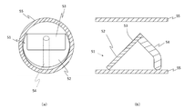
本発明においては、工程(3)において、供給管内で成膜する場合、前記サセプタとして、例えば図19や図20に示されるサセプタを用いるのが好ましい。 In the present invention, when the film is formed in the supply pipe in the step (3), it is preferable to use, for example, the susceptor shown in FIGS. 19 and 20 as the susceptor.
図19は、サセプタの一態様を示している。図19に示されるサセプタ51は、ミスト加速部52、基板保持部53および支持部54を備えている。支持部54は棒状であり、途中で角度を変えて、支持部54の供給管55との接触角を約90°にするように構成されている。このような構成とすることにより、サセプタ51の安定性が向上するが、本発明においては、支持部54の形状については、特に限定されず、適宜、種々の形状を用いることができる。
FIG. 19 shows one aspect of the susceptor. The
図19(a)は、ミストの上流から下流方向に向けて、結晶基板に至るまでの供給管内の断面を示しており、供給管の基板側表面の外周形状が、略半円状であり、前記供給管の内周に沿って略同一となるような形状であることが分かる。図19(b)は、ミストの上流を左に、下流を右にしたときの、供給管、結晶基板およびサセプタの断面を示している。ミストはその性質上、供給管では沈降しやすいが、サセプタ101では、ミスト加速部102が傾斜して設けられており、沈降したミストを加速上昇させて結晶基板103に搬送できるように構成されている。
FIG. 19A shows a cross section of the inside of the supply tube from the upstream to the downstream of the mist to the crystal substrate, and the outer peripheral shape of the substrate side surface of the supply tube is substantially semicircular. It can be seen that the shapes are substantially the same along the inner circumference of the supply pipe. FIG. 19B shows a cross section of the supply pipe, the crystal substrate and the susceptor when the upstream side of the mist is on the left and the downstream side is on the right. Due to its nature, the mist tends to settle in the supply pipe, but in the susceptor 101, the
図20は、供給管55内において、図19に示されるサセプタおよび結晶基板の領域を基板・サセプタ領域61として、未反応のミストを排出する領域を、排出領域62として示しており、サセプタと結晶基板との総面積と、排出領域の面積との関係が分かるようになっている。本発明では、図20に示されるように、前記サセプタが占めるサセプタ領域と、前記基板領域と、未反応のミストを排出する排出領域とに分けられる前記供給管内の断面において、前記サセプタ領域と前記結晶基板との総面積が、前記排出領域の面積よりも大きいことが好ましい。このような好ましいサセプタを用いることにより、結晶基板上でミストを加速させることができ、より均質でより厚い結晶膜を得ることができる。
FIG. 20 shows a region of the susceptor and the crystal substrate shown in FIG. 19 as a substrate /
なお、本発明では、前記結晶膜形成の際に、ドーパントを用いて、ドーピング処理を行うことができる。また、本発明においては、ドーピング処理を、前記原料溶液に異常粒抑制剤を含めて行うのが好ましい。前記原料溶液に異常粒抑制剤を含めてドーピング処理を行うことで、表面平滑性に優れた結晶膜を得ることができる。ドーピング量は、本発明の目的を阻害しない限り、特に限定されないが、原料中、モル比で、0.01〜10%であるのが好ましく、0.1〜5%であるのがより好ましい。 In the present invention, when the crystal film is formed, a doping treatment can be performed using a dopant. Further, in the present invention, it is preferable to carry out the doping treatment by including the abnormal grain inhibitor in the raw material solution. A crystal film having excellent surface smoothness can be obtained by performing a doping treatment in which the raw material solution contains an abnormal grain inhibitor. The doping amount is not particularly limited as long as the object of the present invention is not impaired, but the molar ratio in the raw material is preferably 0.01 to 10%, more preferably 0.1 to 5%.
前記異常粒抑制剤は、成膜過程で副生する粒子の発生を抑制する効果を有するものをいい、結晶膜の表面粗さ(Ra)を例えば0.1μm以下とすることができれば特に限定されないが、本発明においては、Br、I、FおよびClから選択される少なくとも1種からなる異常粒抑制剤であるのが好ましい。安定的に膜形成をするために異常粒抑制剤として、BrやIを膜中に導入すると異常粒成長による表面粗さの悪化を抑制することができる。異常粒抑制剤の添加量は、異常粒を抑制できれば特に限定されないが、原料溶液中、体積比で50%以下であることが好ましく、30%以下であることがより好ましく、1〜30%の範囲内であることが最も好ましい。このような好ましい範囲で異常粒抑制剤を使用することにより、異常粒抑制剤として機能させることができるので、結晶膜の異常粒の成長を抑制して表面を平滑にすることができる。 The abnormal grain inhibitor has an effect of suppressing the generation of particles produced as a by-product in the film forming process, and is not particularly limited as long as the surface roughness (Ra) of the crystal film can be set to, for example, 0.1 μm or less. However, in the present invention, it is preferable that the abnormality grain inhibitor is composed of at least one selected from Br, I, F and Cl. When Br or I is introduced into the film as an abnormal grain inhibitor for stable film formation, deterioration of surface roughness due to abnormal grain growth can be suppressed. The amount of the abnormal grain inhibitor added is not particularly limited as long as the abnormal grains can be suppressed, but it is preferably 50% or less, more preferably 30% or less, and 1 to 30% in volume ratio in the raw material solution. Most preferably within the range. By using the abnormal grain inhibitor in such a preferable range, it can function as an abnormal grain inhibitor, so that the growth of abnormal grains in the crystal film can be suppressed and the surface can be smoothed.
結晶膜の形成方法は、本発明の目的を阻害しない限り、特に限定されないが、例えば、ガリウム化合物及び所望によりインジウム化合物またはアルミニウム化合物等を結晶膜の組成に合わせて組み合わせた原料を反応させることによって形成可能である。つまり、前記原料溶液は、インジウム、アルミニウムおよびガリウムから選ばれる1種または2種以上の金属を含んでいる。これによって、結晶基板上に、基板側から結晶膜を結晶成長させることができる。ガリウム化合物としては、ガリウム金属を出発材料として成膜直前にガリウム化合物に変化させたものであってもよい。ガリウム化合物としては、例えば、ガリウムの有機金属錯体(例:アセチルアセトナート錯体等)やハロゲン化物(例:フッ化、塩化、臭化又はヨウ化物等)などが挙げられるが、本発明においては、ハロゲン化物(例:フッ化、塩化、臭化又はヨウ化物等)を用いることが好ましい。原料化合物にハロゲン化物を用いてミストCVDで成膜することで、前記結晶膜に炭素を実質的に含まないようにすることができる。 The method for forming the crystal film is not particularly limited as long as the object of the present invention is not impaired, but for example, by reacting a raw material in which a gallium compound and, if desired, an indium compound or an aluminum compound are combined according to the composition of the crystal film. It can be formed. That is, the raw material solution contains one or more metals selected from indium, aluminum and gallium. As a result, a crystal film can be crystal-grown on the crystal substrate from the substrate side. As the gallium compound, a gallium metal may be used as a starting material and changed to a gallium compound immediately before film formation. Examples of the gallium compound include an organic metal complex of gallium (eg, acetylacetonate complex, etc.) and a halide (eg, fluoride, chloride, bromide, iodide, etc.). It is preferable to use a halide (eg, fluoride, chloride, bromide, iodide, etc.). By forming a film by mist CVD using a halide as a raw material compound, it is possible to substantially eliminate carbon in the crystal film.
より具体的には、結晶膜は、原料化合物が溶解した原料溶液から生成された原料微粒子を成膜室に供給して、前記サセプタを用いて、前記成膜室内で前記原料化合物を熱反応させることによって形成することができる。原料溶液の溶媒は、特に限定されないが、水、過酸化水素水または有機溶媒であることが好ましい。本発明においては、通常、ドーパント原料の存在下で、上記原料化合物を反応させる。なお、ドーパント原料は、好ましくは、原料溶液に含められて、原料化合物と共に又は別々に微粒子化される。前記結晶膜に含まれる炭素が、ドーパントよりも少なくなり、好ましくは、前記結晶膜に炭素を実質的に含まないようにことができる。なお、本発明の結晶膜が、ハロゲン(好ましくはBr)を含むのも良好な半導体特性を発揮するため好ましい。ドーパント原料としては、例えば、スズ、ゲルマニウム、ケイ素、チタン、ジルコニウム、バナジウムまたはニオブの金属単体又は化合物(例:ハロゲン化物、酸化物等)などが挙げられる。 More specifically, in the crystal film, raw material fine particles generated from a raw material solution in which a raw material compound is dissolved are supplied to a film forming chamber, and the raw material compound is thermally reacted in the film forming chamber using the susceptor. Can be formed by The solvent of the raw material solution is not particularly limited, but is preferably water, hydrogen peroxide solution, or an organic solvent. In the present invention, the raw material compound is usually reacted in the presence of a dopant raw material. The dopant raw material is preferably contained in the raw material solution and micronized together with or separately from the raw material compound. The amount of carbon contained in the crystal film is less than that of the dopant, and preferably, the crystal film can be substantially free of carbon. It is also preferable that the crystal film of the present invention contains a halogen (preferably Br) because it exhibits good semiconductor characteristics. Examples of the dopant raw material include simple substances or compounds of tin, germanium, silicon, titanium, zirconium, vanadium or niobium (eg, halides, oxides, etc.).
以上のようにして成膜することにより、工業的有利に、結晶性に優れた結晶膜を得ることができる。また、上記の好ましい方法で結晶基板上に結晶膜を成膜することにより、原子間力顕微鏡を用いて測定される結晶膜の膜表面の中心線平均粗さ(Ra)が10nm以下であり、最大高低差(P−V値)が100nm以下とすることができる。なお、本発明においては、成膜時間を適宜調整することにより、結晶性を損なわずに、膜厚を1μm以上とすることができ、好ましくは3μm以上とすることができる。 By forming the film as described above, it is possible to obtain a crystal film having excellent crystallinity, which is industrially advantageous. Further, by forming a crystal film on the crystal substrate by the above preferable method, the centerline average roughness (Ra) of the film surface of the crystal film measured by an atomic force microscope is 10 nm or less. The maximum height difference (PV value) can be 100 nm or less. In the present invention, the film thickness can be set to 1 μm or more, preferably 3 μm or more, without impairing the crystallinity by appropriately adjusting the film forming time.
本発明においては、成膜後、アニール処理を行ってもよい。アニール処理の温度は、特に限定されないが、700℃以下が好ましく、300℃〜700℃がより好ましく、300℃〜550℃が最も好ましい。このような好ましい温度でアニール処理を行うことにより、より好適に前記結晶膜のキャリア濃度を調節することができる。アニール処理の処理時間は、本発明の目的を阻害しない限り、特に限定されないが、10秒〜10時間であるのが好ましく、10秒〜1時間であるのがより好ましい。 In the present invention, annealing treatment may be performed after the film formation. The temperature of the annealing treatment is not particularly limited, but is preferably 700 ° C. or lower, more preferably 300 ° C. to 700 ° C., and most preferably 300 ° C. to 550 ° C. By performing the annealing treatment at such a preferable temperature, the carrier concentration of the crystal film can be adjusted more preferably. The treatment time of the annealing treatment is not particularly limited as long as the object of the present invention is not impaired, but is preferably 10 seconds to 10 hours, and more preferably 10 seconds to 1 hour.
前記積層構造体は、前記結晶性酸化物が半導体である場合には、前記積層構造体をそのままで又は所望により更に加工等の処理を施して、半導体装置に用いることができる。また、半導体装置に用いる場合には、そのまま半導体装置に用いてもよいし、さらに他の層(例えば絶縁体層、半絶縁体層、導体層、半導体層、緩衝層またはその他中間層等)などを形成してもよい。 When the crystalline oxide is a semiconductor, the laminated structure can be used in a semiconductor device as it is or by further processing the laminated structure as desired. When used in a semiconductor device, it may be used as it is in a semiconductor device, or another layer (for example, an insulator layer, a semi-insulator layer, a conductor layer, a semiconductor layer, a buffer layer, or another intermediate layer) or the like. May be formed.
本発明の積層構造体は、様々な半導体装置に有用であり、とりわけ、パワーデバイスに有用である。また、半導体装置は、電極が半導体層の片面側に形成された横型の素子(横型デバイス)と、半導体層の表裏両面側にそれぞれ電極を有する縦型の素子(縦型デバイス)に分類することができ、本発明においては、前記積層構造体を横型デバイスにも縦型デバイスにも好適に用いることができる。前記半導体装置としては、例えば、ショットキーバリアダイオード(SBD)、金属半導体電界効果トランジスタ(MESFET)、高電子移動度トランジスタ(HEMT)、金属酸化膜半導体電界効果トランジスタ(MOSFET)、静電誘導トランジスタ(SIT)、接合電界効果トランジスタ(JFET)、絶縁ゲート型バイポーラトランジスタ(IGBT)または発光ダイオードなどが挙げられる。本発明においては、前記半導体装置が、SBD、MOSFET、SIT、JFETまたはIGBTであるのが好ましく、SBD、MOSFETまたはSITであるのがより好ましい。また、本発明においては、前記半導体装置が、p型半導体層を含まないものであってもよい。 The laminated structure of the present invention is useful for various semiconductor devices, and is particularly useful for power devices. In addition, semiconductor devices are classified into horizontal elements (horizontal devices) in which electrodes are formed on one side of the semiconductor layer and vertical elements (vertical devices) in which electrodes are provided on both the front and back sides of the semiconductor layer. In the present invention, the laminated structure can be suitably used for both horizontal devices and vertical devices. Examples of the semiconductor device include a Schottky barrier diode (SBD), a metal semiconductor field effect transistor (MESFET), a high electron mobility transistor (HEMT), a metal oxide film semiconductor field effect transistor (MOSFET), and an electrostatic induction transistor (MSFET). SIT), junction field effect transistor (JFET), insulated gate bipolar transistor (IGBT), light emitting diode and the like. In the present invention, the semiconductor device is preferably an SBD, MOSFET, SIT, JFET or IGBT, and more preferably an SBD, MOSFET or SIT. Further, in the present invention, the semiconductor device may not include a p-type semiconductor layer.
以下、前記半導体構造の結晶性半導体膜をn型半導体層(n+型半導体やn−型半導体等)に適用した場合の好適な例を、図面を用いて説明するが、本発明は、これらの例に限定されるものではない。なお、以下に例示する半導体装置において、本発明の目的を阻害しない限り、さらに他の層(例えば絶縁体層、半絶縁体層、導体層、半導体層、緩衝層またはその他中間層等)などが含まれていてもよいし、また、緩衝層(バッファ層)なども適宜省いてもよい。 Hereinafter, suitable examples when the crystalline semiconductor film having the semiconductor structure is applied to an n-type semiconductor layer (n + type semiconductor, n-type semiconductor, etc.) will be described with reference to the drawings. It is not limited to the example. In the semiconductor device exemplified below, other layers (for example, an insulator layer, a semi-insulator layer, a conductor layer, a semiconductor layer, a buffer layer, another intermediate layer, etc.) may be used as long as the object of the present invention is not impaired. It may be contained, and the buffer layer (buffer layer) and the like may be omitted as appropriate.
(SBD)
図1は、本発明に係るショットキーバリアダイオード(SBD)の一例を示している。図1のSBDは、n−型半導体層101a、n+型半導体層101b、ショットキー電極105aおよびオーミック電極105bを備えている。(SBD)
FIG. 1 shows an example of a Schottky barrier diode (SBD) according to the present invention. The SBD of FIG. 1 includes an n-
ショットキー電極およびオーミック電極の材料は、公知の電極材料であってもよく、前記電極材料としては、例えば、Al、Mo、Co、Zr、Sn、Nb、Fe、Cr、Ta、Ti、Au、Pt、V、Mn、Ni、Cu、Hf、W、Ir、Zn、In、Pd、NdもしくはAg等の金属またはこれらの合金、酸化錫、酸化亜鉛、酸化インジウム、酸化インジウム錫(ITO)、酸化亜鉛インジウム(IZO)等の金属酸化物導電膜、ポリアニリン、ポリチオフェン又はポリピロ−ルなどの有機導電性化合物、またはこれらの混合物などが挙げられる。 The material of the Schottky electrode and the ohmic electrode may be a known electrode material, and the electrode material includes, for example, Al, Mo, Co, Zr, Sn, Nb, Fe, Cr, Ta, Ti, Au, etc. Metals such as Pt, V, Mn, Ni, Cu, Hf, W, Ir, Zn, In, Pd, Nd or Ag or alloys thereof, tin oxide, zinc oxide, indium oxide, indium tin oxide (ITO), oxidation Examples thereof include metal oxide conductive films such as indium tin oxide (IZO), organic conductive compounds such as polyaniline, polythiophene or polypyrrole, or mixtures thereof.
ショットキー電極およびオーミック電極の形成は、例えば、真空蒸着法またはスパッタリング法などの公知の手段により行うことができる。より具体的に例えば、ショットキー電極を形成する場合、Moからなる層とAlからなる層を積層させ、Moからなる層およびAlからなる層に対して、フォトリソグラフィの手法を利用したパターニングを施すことにより行うことができる。 The Schottky electrode and the ohmic electrode can be formed by a known means such as a vacuum vapor deposition method or a sputtering method. More specifically, for example, when forming a Schottky electrode, a layer made of Mo and a layer made of Al are laminated, and the layer made of Mo and the layer made of Al are patterned using a photolithography technique. It can be done by.
図1のSBDに逆バイアスが印加された場合には、空乏層(図示せず)がn−型半導体層101aの中に広がるため、高耐圧のSBDとなる。また、順バイアスが印加された場合には、オーミック電極105bからショットキー電極105aへ電子が流れる。このようにして前記半導体構造を用いたSBDは、高耐圧・大電流用に優れており、スイッチング速度も速く、耐圧性・信頼性にも優れている。
When a reverse bias is applied to the SBD of FIG. 1, the depletion layer (not shown) spreads in the n-
図2は、本発明に係るショットキーバリアダイオード(SBD)の一例を示している。図2のSBDは、図1のSBDの構成に加え、さらに絶縁体層104を備えている。より具体的には、n−型半導体層101a、n+型半導体層101b、ショットキー電極105a、オーミック電極105bおよび絶縁体層104を備えている。
FIG. 2 shows an example of a Schottky barrier diode (SBD) according to the present invention. The SBD of FIG. 2 further includes an
絶縁体層104の材料としては、例えば、GaO、AlGaO、InAlGaO、AlInZnGaO4、AlN、Hf2O3、SiN、SiON、Al2O3、MgO、GdO、SiO2またはSi3N4などが挙げられるが、本発明においては、コランダム構造を有するものであるのが好ましい。コランダム構造を有する絶縁体を絶縁体層に用いることで、界面における半導体特性の機能を良好に発現させることができる。絶縁体層104は、n−型半導体層101とショットキー電極105aとの間に設けられている。絶縁体層の形成は、例えば、スパッタリング法、真空蒸着法またはCVD法などの公知の手段により行うことができる。Examples of the material of the
ショットキー電極やオーミック電極の形成や材料等については、上記図1のSBDの場合と同様であり、例えばスパッタリング法、真空蒸着法、圧着法、CVD法等の公知の手段を用いて、例えば、Al、Mo、Co、Zr、Sn、Nb、Fe、Cr、Ta、Ti、Au、Pt、V、Mn、Ni、Cu、Hf、W、Ir、Zn、In、Pd、NdもしくはAg等の金属またはこれらの合金、酸化錫、酸化亜鉛、酸化インジウム、酸化インジウム錫(ITO)、酸化亜鉛インジウム(IZO)等の金属酸化物導電膜、ポリアニリン、ポリチオフェン又はポリピロ−ルなどの有機導電性化合物、またはこれらの混合物などからなる電極を形成することができる。 The formation of the Schottky electrode and the ohmic electrode, the material, and the like are the same as in the case of the SBD shown in FIG. Metals such as Al, Mo, Co, Zr, Sn, Nb, Fe, Cr, Ta, Ti, Au, Pt, V, Mn, Ni, Cu, Hf, W, Ir, Zn, In, Pd, Nd or Ag Or these alloys, metal oxide conductive films such as tin oxide, zinc oxide, indium oxide, indium tin oxide (ITO), indium zinc oxide (IZO), organic conductive compounds such as polyaniline, polythiophene or polypyrrole, or An electrode made of a mixture of these can be formed.
図2のSBDは、図1のSBDに比べ、さらに絶縁特性に優れており、より高い電流制御性を有する。 The SBD of FIG. 2 is further excellent in insulation characteristics and has higher current controllability than the SBD of FIG.
図3のSBDは、本発明に係るショットキーバリアダイオード(SBD)の一例を示している。図3のSBDは、図1や図2のSBDの構成とは、トレンチ構造を有しており、半絶縁体層103を備えている点で大きく異なっている。図3のSBDは、n−型半導体層101a、n+型半導体層101b、ショットキー電極105a、オーミック電極105bおよび半絶縁体層103を備えており、耐圧性を維持したまま、リーク電流を大幅に低減することができ、大幅な低オン抵抗化も可能となる。
The SBD in FIG. 3 shows an example of a Schottky barrier diode (SBD) according to the present invention. The SBD of FIG. 3 is significantly different from the SBD of FIGS. 1 and 2 in that it has a trench structure and includes a
半絶縁体層103は、半絶縁体で構成されていればそれでよく、前記半絶縁体としては、例えば、マグネシウム(Mg)、ルテニウム(Ru)、鉄(Fe)、ベリリウム(Be)、セシウム(Cs)、ストロンチウム、バリウム等の半絶縁体ドーパントを含むものやドーピング処理がなされていないもの等が挙げられる。
The
(MESFET)
図4は、本発明に係る金属半導体電界効果トランジスタ(MESFET)の一例を示している。図4のMESFETは、n−型半導体層111a、n+型半導体層111b、緩衝層(バッファ層)118、半絶縁体層114、ゲート電極115a、ソース電極115bおよびドレイン電極115cを備えている。(MESFET)
FIG. 4 shows an example of a metal semiconductor field effect transistor (MESFET) according to the present invention. The MESFET of FIG. 4 includes an n-
ゲート電極、ドレイン電極およびソース電極の材料は、公知の電極材料であってもよく、前記電極材料としては、例えば、Al、Mo、Co、Zr、Sn、Nb、Fe、Cr、Ta、Ti、Au、Pt、V、Mn、Ni、Cu、Hf、W、Ir、Zn、In、Pd、NdもしくはAg等の金属またはこれらの合金、酸化錫、酸化亜鉛、酸化インジウム、酸化インジウム錫(ITO)、酸化亜鉛インジウム(IZO)等の金属酸化物導電膜、ポリアニリン、ポリチオフェン又はポリピロ−ルなどの有機導電性化合物、またはこれらの混合物などが挙げられる。ゲート電極、ドレイン電極およびソース電極の形成は、例えば、真空蒸着法またはスパッタリング法などの公知の手段により行うことができる。 The material of the gate electrode, the drain electrode and the source electrode may be a known electrode material, and examples of the electrode material include Al, Mo, Co, Zr, Sn, Nb, Fe, Cr, Ta and Ti. Metals such as Au, Pt, V, Mn, Ni, Cu, Hf, W, Ir, Zn, In, Pd, Nd or Ag or alloys thereof, tin oxide, zinc oxide, indium oxide, indium tin oxide (ITO) , Metal oxide conductive film such as indium tin oxide (IZO), organic conductive compound such as polyaniline, polythiophene or polypyrrole, or a mixture thereof. The gate electrode, drain electrode and source electrode can be formed by a known means such as a vacuum vapor deposition method or a sputtering method.
半絶縁体層114は、半絶縁体で構成されていればそれでよく、前記半絶縁体としては、例えば、マグネシウム(Mg)、ルテニウム(Ru)、鉄(Fe)、ベリリウム(Be)、セシウム(Cs)、ストロンチウム、バリウム等の半絶縁体ドーパントを含むものやドーピング処理がなされていないもの等が挙げられる。
The
図4のMESFETでは、ゲート電極下に良好な空乏層が形成されるので、ドレイン電極からソース電極に流れる電流を効率よく制御することができる。 In the MESFET of FIG. 4, since a good depletion layer is formed under the gate electrode, the current flowing from the drain electrode to the source electrode can be efficiently controlled.
(HEMT)
図5は、本発明に係る光電子移動度トランジスタ(HEMT)の一例を示している。図5のHEMTは、バンドギャップの広いn型半導体層121a、バンドギャップの狭いn型半導体層121b、n+型半導体層121c、半絶縁体層124、緩衝層128、ゲート電極125a、ソース電極125bおよびドレイン電極125cを備えている。(HEMT)
FIG. 5 shows an example of a photoelectron mobility transistor (HEMT) according to the present invention. The HEMT of FIG. 5 includes an n-
ゲート電極、ドレイン電極およびソース電極の材料は、それぞれ公知の電極材料であってもよく、前記電極材料としては、例えば、Al、Mo、Co、Zr、Sn、Nb、Fe、Cr、Ta、Ti、Au、Pt、V、Mn、Ni、Cu、Hf、W、Ir、Zn、In、Pd、NdもしくはAg等の金属またはこれらの合金、酸化錫、酸化亜鉛、酸化インジウム、酸化インジウム錫(ITO)、酸化亜鉛インジウム(IZO)等の金属酸化物導電膜、ポリアニリン、ポリチオフェン又はポリピロ−ルなどの有機導電性化合物、またはこれらの混合物などが挙げられる。ゲート電極、ドレイン電極およびソース電極の形成は、例えば、真空蒸着法またはスパッタリング法などの公知の手段により行うことができる。 The material of the gate electrode, the drain electrode, and the source electrode may be known electrode materials, and the electrode materials include, for example, Al, Mo, Co, Zr, Sn, Nb, Fe, Cr, Ta, and Ti. , Au, Pt, V, Mn, Ni, Cu, Hf, W, Ir, Zn, In, Pd, Nd or Ag or other metals or alloys thereof, tin oxide, zinc oxide, indium oxide, indium tin oxide (ITO) ), Metal oxide conductive films such as indium tin oxide (IZO), organic conductive compounds such as polyaniline, polythiophene or polypyrrole, or mixtures thereof. The gate electrode, drain electrode and source electrode can be formed by a known means such as a vacuum vapor deposition method or a sputtering method.
なお、ゲート電極下のn型半導体層は、少なくともバンドギャップの広い層121aと狭い層121bとで構成されており、半絶縁体層124は、半絶縁体で構成されていればそれでよく、前記半絶縁体としては、例えばルテニウム(Ru)や鉄(Fe)等の半絶縁体ドーパントを含むものやドーピング処理がなされていないもの等が挙げられる。
図5のHEMTでは、ゲート電極下に良好な空乏層が形成されるので、ドレイン電極からソース電極に流れる電流を効率よく制御することができる。また、本発明においては、さらにリセス構造とすることで、ノーマリーオフを発現することができる。The n-type semiconductor layer under the gate electrode is composed of at least a
In the HEMT of FIG. 5, since a good depletion layer is formed under the gate electrode, the current flowing from the drain electrode to the source electrode can be efficiently controlled. Further, in the present invention, the normally off can be expressed by further adopting the recess structure.
(MOSFET)
本発明の半導体装置がMOSFETである場合の一例を図6に示す。図6のMOSFETは、トレンチ型のMOSFETであり、n−型半導体層131a、n+型半導体層131b及び131c、ゲート絶縁膜134、ゲート電極135a、ソース電極135bおよびドレイン電極135cを備えている。(MOSFET)
FIG. 6 shows an example of the case where the semiconductor device of the present invention is a MOSFET. The MOSFET of FIG. 6 is a trench-type MOSFET, and includes an n-
ドレイン電極135c上には、例えば厚さ100nm〜100μmのn+型半導体層131bが形成されており、前記n+型半導体層131b上には、例えば厚さ100nm〜100μmのn−型半導体層131aが形成されている。そして、さらに、前記n−型半導体層131a上には、n+型半導体層131cが形成されており、前記n+型半導体層131c上には、ソース電極135bが形成されている。
An n +
また、前記n−型半導体層131a及び前記n+型半導体層131c内には、前記n+半導体層131cを貫通し、前記n−型半導体層131aの途中まで達する深さの複数のトレンチ溝が形成されている。前記トレンチ溝内には、例えば、10nm〜1μmの厚みのゲート絶縁膜134を介してゲート電極135aが埋め込み形成されている。
Further, in the n−
図6のMOSFETのオン状態では、前記ソース電極135bと前記ドレイン電極135cとの間に電圧を印可し、前記ゲート電極135aに前記ソース電極135bに対して正の電圧を与えると、前記n−型半導体層131aの側面にチャネル層が形成され、電子が前記n−型半導体層131aに注入され、ターンオンする。オフ状態は、前記ゲート電極の電圧を0Vにすることにより、チャネル層ができなくなり、n−型半導体層131aが空乏層で満たされた状態になり、ターンオフとなる。
In the ON state of the MOSFET of FIG. 6, when a voltage is applied between the
図7は、図6のMOSFETの製造工程の一部を示している。例えば図7(a)に示すような半導体構造を用いて、n−型半導体層131aおよびn+型半導体層131cの所定領域にエッチングマスクを設け、前記エッチングマスクをマスクにして、さらに、反応性イオンエッチング法等により異方性エッチングを行って、図7(b)に示すように、前記n+型半導体層131c表面から前記n−型半導体層131aの途中にまで達する深さのトレンチ溝を形成する。次いで、図7(c)に示すように、熱酸化法、真空蒸着法、スパッタリング法、CVD法等の公知の手段を用いて、前記トレンチ溝の側面及び底面に、例えば50nm〜1μm厚のゲート絶縁膜134を形成した後、CVD法、真空蒸着法、スパッタリング法等を用いて、前記トレンチ溝に、例えばポリシリコン等のゲート電極材料をn−型半導体層131aの厚み以下に形成する。
FIG. 7 shows a part of the manufacturing process of the MOSFET of FIG. For example, using the semiconductor structure as shown in FIG. 7A, an etching mask is provided in a predetermined region of the n-
そして、真空蒸着法、スパッタリング法、CVD法等の公知の手段を用いて、n+型半導体層131c上にソース電極135bを、n+型半導体層131b上にドレイン電極135cを、それぞれ形成することで、パワーMOSFETを製造することができる。なお、ソース電極およびドレイン電極の電極材料は、それぞれ公知の電極材料であってもよく、前記電極材料としては、例えば、Al、Mo、Co、Zr、Sn、Nb、Fe、Cr、Ta、Ti、Au、Pt、V、Mn、Ni、Cu、Hf、W、Ir、Zn、In、Pd、NdもしくはAg等の金属またはこれらの合金、酸化錫、酸化亜鉛、酸化インジウム、酸化インジウム錫(ITO)、酸化亜鉛インジウム(IZO)等の金属酸化物導電膜、ポリアニリン、ポリチオフェン又はポリピロ−ルなどの有機導電性化合物、またはこれらの混合物などが挙げられる。
Then, the
このようにして得られたMOSFETは、従来のトレンチ型MOSFETに比べて、さらに耐圧性に優れたものとなる。なお、図6では、トレンチ型の縦型MOSFETの例を示したが、本発明においては、これに限定されず、種々のMOSFETの形態に適用可能である。例えば、図6のトレンチ溝の深さをn−型半導体層131aの底面まで達する深さまで掘り下げて、シリーズ抵抗を低減させるようにしてもよい。なお、横型のMOSFETの場合の一例を図8に示す。図8のMOSFETは、n−型半導体層131a、第1のn+型半導体層131b、第2のn+型半導体層131c、ゲート絶縁膜134、ゲート電極135a、ソース電極135b、ドレイン電極135c、緩衝層138および半絶縁体層139を備えている。図8に示すように、n+型半導体層をn−型半導体層に埋め込むことで、他の横型のMOSFETに比べ、より良好に電流を流すことができる。
The MOSFET obtained in this way has further excellent withstand voltage as compared with the conventional trench-type MOSFET. Although FIG. 6 shows an example of a trench-type vertical MOSFET, the present invention is not limited to this, and can be applied to various MOSFET forms. For example, the depth of the trench groove in FIG. 6 may be dug down to a depth reaching the bottom surface of the n-
(SIT)
図9は、本発明の半導体装置がSITである場合の一例を示す。図9のSITは、n−型半導体層141a、n+型半導体層141b及び141c、ゲート電極145a、ソース電極145bおよびドレイン電極145cを備えている。(SIT)
FIG. 9 shows an example of a case where the semiconductor device of the present invention is a SIT. The SIT of FIG. 9 includes an n-
ドレイン電極145c上には、例えば厚さ100nm〜100μmのn+型半導体層141bが形成されており、前記n+型半導体層141b上には、例えば厚さ100nm〜100μmのn−型半導体層141aが形成されている。そして、さらに、前記n−型半導体層141a上には、n+型半導体層141cが形成されており、前記n+型半導体層141c上には、ソース電極145bが形成されている。
For example, an n +
また、前記n−型半導体層141a内には、前記n+半導体層141cを貫通し、前記n−半導体層141aの途中の深さまで達する深さの複数のトレンチ溝が形成されている。前記トレンチ溝内のn−型半導体層上には、ゲート電極145aが形成されている。
図9のSITのオン状態では、前記ソース電極145bと前記ドレイン電極145cとの間に電圧を印可し、前記ゲート電極145aに前記ソース電極145bに対して正の電圧を与えると、前記n−型半導体層141a内にチャネル層が形成され、電子が前記n−型半導体層141aに注入され、ターンオンする。オフ状態は、前記ゲート電極の電圧を0Vにすることにより、チャネル層ができなくなり、n−型半導体層141aが空乏層で満たされた状態になり、ターンオフとなる。Further, in the n-
When the SIT in FIG. 9 is on, a voltage is applied between the
図9に示されるSITの製造には、公知の手段を用いることができる。例えば、図7(a)に示される半導体構造を用いて、上記の図7のMOSFETの製造工程と同様にして、n−型半導体層141aおよびn+型半導体層141cの所定領域にエッチングマスクを設け、前記エッチングマスクをマスクにして、例えば、反応性イオンエッチング法等により異方性エッチングを行って、前記n+型半導体層141c表面から前記n−型半導体層の途中まで達する深さのトレンチ溝を形成する。次いで、CVD法、真空蒸着法、スパッタリング法等で、前記トレンチ溝に、例えばポリシリコン等のゲート電極材料をn−型半導体層141aの厚み以下に形成する。そして、真空蒸着法、スパッタリング法、CVD法等の公知の手段を用いて、n+型半導体層141c上にソース電極145bを、n+型半導体層141b上にドレイン電極145cを、それぞれ形成することで、図9に示されるSITを製造することができる。
Known means can be used in the production of the SIT shown in FIG. For example, using the semiconductor structure shown in FIG. 7A, etching masks are provided in predetermined regions of the n-
なお、ソース電極およびドレイン電極の電極材料は、それぞれ公知の電極材料であってもよく、前記電極材料としては、例えば、Al、Mo、Co、Zr、Sn、Nb、Fe、Cr、Ta、Ti、Au、Pt、V、Mn、Ni、Cu、Hf、W、Ir、Zn、In、Pd、NdもしくはAg等の金属またはこれらの合金、酸化錫、酸化亜鉛、酸化インジウム、酸化インジウム錫(ITO)、酸化亜鉛インジウム(IZO)等の金属酸化物導電膜、ポリアニリン、ポリチオフェン又はポリピロ−ルなどの有機導電性化合物、またはこれらの混合物などが挙げられる。 The electrode materials of the source electrode and the drain electrode may be known electrode materials, respectively, and the electrode materials include, for example, Al, Mo, Co, Zr, Sn, Nb, Fe, Cr, Ta, and Ti. , Au, Pt, V, Mn, Ni, Cu, Hf, W, Ir, Zn, In, Pd, Nd or Ag or other metals or alloys thereof, tin oxide, zinc oxide, indium oxide, indium tin oxide (ITO) ), Metal oxide conductive films such as indium tin oxide (IZO), organic conductive compounds such as polyaniline, polythiophene or polypyrrole, or mixtures thereof.
上記例では、p型半導体を使用していない例を示したが、本発明においては、これに限定されず、p型半導体を用いてもよい。p型半導体を用いた例を図10〜16に示す。これらの半導体装置は、上記例と同様にして製造することができる。なお、p型半導体は、n型半導体と同じ材料であって、p型ドーパントを含むものであってもよいし、異なるp型半導体であってもよい。 In the above example, an example in which a p-type semiconductor is not used is shown, but the present invention is not limited to this, and a p-type semiconductor may be used. Examples of using a p-type semiconductor are shown in FIGS. 10 to 16. These semiconductor devices can be manufactured in the same manner as in the above example. The p-type semiconductor may be the same material as the n-type semiconductor and may contain a p-type dopant, or may be a different p-type semiconductor.
図10は、n−型半導体層101a、n+型半導体層101b、p型半導体層102、絶縁体層104、ショットキー電極105aおよびオーミック電極105bを備えているショットキーバリアダイオード(SBD)の好適な一例を示す。
FIG. 10 shows a suitable Schottky barrier diode (SBD) including an n-
図11は、n−型半導体層101a、n+型半導体層101b、p型半導体層102、ショットキー電極105aおよびオーミック電極105bを備えているトレンチ型のショットキーバリアダイオード(SBD)の好適な一例を示す。トレンチ型のSBDによれば、耐圧性を維持したまま、リーク電流を大幅に低減することができ、大幅な低オン抵抗化も可能となる。
FIG. 11 shows a preferred example of a trench-type Schottky barrier diode (SBD) including an n-
図12は、バンドギャップの広いn型半導体層121a、バンドギャップの狭いn型半導体層121b、n+型半導体層121c、p型半導体層123、ゲート電極125a、ソース電極125b、ドレイン電極125cおよび基板129を備えている高電子移動度トランジスタ(HEMT)の好適な一例を示す。
FIG. 12 shows an n-
図13は、n−型半導体層131a、第1のn+型半導体層131b、第2のn+型半導体層131c、p型半導体層132、p+型半導体層132a、ゲート絶縁膜134、ゲート電極135a、ソース電極135bおよびドレイン電極135cを備えている金属酸化膜半導体電界効果トランジスタ(MOSFET)の好適な一例を示す。なお、p+型半導体層132aは、p型半導体層であってもよく、p型半導体層132と同じであってもよい。
FIG. 13 shows an n-
図14は、n−型半導体層141a、第1のn+型半導体層141b、第2のn+型半導体層141c、p型半導体層142、ゲート電極145a、ソース電極145bおよびドレイン電極145cを備えている接合電界効果トランジスタ(JFET)の好適な一例を示す。
FIG. 14 includes an n-
図15は、n型半導体層151、n−型半導体層151a、n+型半導体層151b、p型半導体層152、ゲート絶縁膜154、ゲート電極155a、エミッタ電極155bおよびコレクタ電極155cを備えている絶縁ゲート型バイポーラトランジスタ(IGBT)の好適な一例を示す。
FIG. 15 shows an insulation provided with an n-
(LED)
本発明の半導体装置が発光ダイオード(LED)である場合の一例を図16に示す。図16の半導体発光素子は、第2の電極165b上にn型半導体層161を備えており、n型半導体層161上には、発光層163が積層されている。そして、発光層163上には、p型半導体層162が積層されている。p型半導体層162上には、発光層163が発生する光を透過する透光性電極167を備えており、透光性電極167上には、第1の電極165aが積層されている。なお、図16の半導体発光素子は、電極部分を除いて保護層で覆われていてもよい。(LED)
FIG. 16 shows an example of the case where the semiconductor device of the present invention is a light emitting diode (LED). The semiconductor light emitting device of FIG. 16 includes an n-
透光性電極の材料としては、インジウム(In)またはチタン(Ti)を含む酸化物の導電性材料などが挙げられる。より具体的には、例えば、In2O3、ZnO、SnO2、Ga2O3、TiO2、CeO2またはこれらの2以上の混晶またはこれらにドーピングされたものなどが挙げられる。これらの材料を、スパッタリング等の公知の手段で設けることによって、透光性電極を形成できる。また、透光性電極を形成した後に、透光性電極の透明化を目的とした熱アニールを施してもよい。Examples of the material of the translucent electrode include a conductive material of an oxide containing indium (In) or titanium (Ti). More specifically, for example, In 2 O 3 , ZnO, SnO 2 , Ga 2 O 3 , TiO 2 , CeO 2, or a mixed crystal of two or more of these, or those doped with these can be mentioned. A translucent electrode can be formed by providing these materials by a known means such as sputtering. Further, after forming the translucent electrode, thermal annealing may be performed for the purpose of making the translucent electrode transparent.
図16の半導体発光素子によれば、第1の電極165aを正極、第2の電極165bを負極とし、両者を介してp型半導体層162、発光層163およびn型半導体層161に電流を流すことで、発光層163が発光するようになっている。
According to the semiconductor light emitting device of FIG. 16, the
第1の電極165a及び第2の電極165bの材料としては、例えば、Al、Mo、Co、Zr、Sn、Nb、Fe、Cr、Ta、Ti、Au、Pt、V、Mn、Ni、Cu、Hf、W、Ir、Zn、In、Pd、NdもしくはAg等の金属またはこれらの合金、酸化錫、酸化亜鉛、酸化インジウム、酸化インジウム錫(ITO)、酸化亜鉛インジウム(IZO)等の金属酸化物導電膜、ポリアニリン、ポリチオフェン又はポリピロ−ルなどの有機導電性化合物、またはこれらの混合物などが挙げられる。電極の形成法は特に限定されることはなく、印刷方式、スプレー法、コ−ティング方式等の湿式方式、真空蒸着法、スパッタリング法、イオンプレ−ティング法等の物理的方式、CVD、プラズマCVD法等の化学的方式などの中から前記材料との適性を考慮して適宜選択した方法に従って前記基板上に形成することができる。
The materials of the
なお、発光素子の別の態様を図17に示す。図17の発光素子では、基板169上にn型半導体層161が積層されており、p型半導体層162、発光層163およびn型半導体層161の一部を切り欠くことによって露出したn型半導体層161の半導体層露出面上の一部に第2の電極165bが積層されている。
Another aspect of the light emitting element is shown in FIG. In the light emitting device of FIG. 17, an n-
以下、本発明の実施例を説明する。 Hereinafter, examples of the present invention will be described.
<実施例1>
1.成膜装置
図18を用いて、本実施例で用いたミストCVD装置19を説明する。ミストCVD装置19は、基板20を載置するサセプタ21と、キャリアガスを供給するキャリアガス供給手段22と、キャリアガス供給手段22から送り出されるキャリアガスの流量を調節するための流量調節弁23と、原料溶液24aが収容されるミスト発生源24と、水25aが入れられる容器25と、容器25の底面に取り付けられた超音波振動子26と、内径40mmの石英管からなる供給管27と、供給管27の周辺部に設置されたヒーター28を備えている。サセプタ21は、石英からなり、基板20を載置する面が水平面から傾斜している。供給管27とサセプタ21をどちらも石英で作製することにより、基板20上に形成される膜内に装置由来の不純物が混入することを抑制している。
なお、サセプタ21として、図19に示されるサセプタ51を用いた。なお、サセプタの傾斜角を45°とし、供給管内の基板・サセプタの総面積を、図19に示される通り、サセプタ領域を徐々に大きくなるようにし、排出領域を徐々に狭くなるようにし、図20に示される通り、サセプタ領域を排出領域よりも大きくなるように構成した。<Example 1>
1. 1. Film formation device The
As the
2.原料溶液と結晶基板の調整
臭化ガリウムと酸化ゲルマニウムをガリウムに対するゲルマニウムの原子比が1:0.05となるように水溶液を調整した。この際、48%臭化水素酸溶液を体積比で10%を含有させた。条件1では、酸化ゲルマニウムの濃度は、5.0×10⁻³mol/Lとした。この原料溶液24aをミスト発生源24内に収容した。また、結晶基板20として、0.2°のオフ角を有するc面サファイア基板(1辺が10mmの正方形で厚さ600μm)を用いた。2. Preparation of raw material solution and crystal substrate The aqueous solution of gallium bromide and germanium oxide was adjusted so that the atomic ratio of germanium to gallium was 1: 0.05. At this time, a 48% hydrobromic acid solution was contained at a volume ratio of 10%. Under condition 1, the concentration of germanium oxide was 5.0 × 10 -3 mol / L. This
3.成膜準備
結晶基板20をサセプタ21上に設置させ、ヒーター28を作動させて供給管27内の温度を500℃にまで昇温させた。次に、流量調節弁23を開いてキャリアガス源22からキャリアガスを供給管27内に供給し、供給管27の雰囲気をキャリアガスで十分に置換した後、キャリアガスの流量を5L/minに調節した。キャリアガスとしては、酸素ガスを用いた。3. 3. Preparation for film formation The
4.膜形成
次に、超音波振動子26を2.4MHzで振動させ、その振動を、水25aを通じて原料溶液24aに伝播させることによって、原料溶液24aを微粒子化させて、原料微粒子を生成した。
この原料微粒子が、キャリアガスによって供給管27内に導入され、供給管27内で反応して、結晶基板20の成膜面でのCVD反応によって結晶基板20上に膜を積層し、積層構造体を得た。4. Film formation Next, the
The raw material fine particles are introduced into the
5.評価
得られた結晶膜は、白濁もなく、きれいな結晶であった。また、得られた結晶膜の相の同定をした。同定は、XRD回折装置を用いて、15度から95度の角度で2θ/ωスキャンを行うことにより行った。測定は、CuKα線を用いて行った。その結果、得られた膜はα−Ga203であった。また、得られた結晶性半導体膜の膜厚は3.5μmであった。5. Evaluation The obtained crystal film was a clean crystal without cloudiness. In addition, the phase of the obtained crystal film was identified. Identification was performed by performing a 2θ / ω scan at an angle of 15 to 95 degrees using an XRD diffractometer. The measurement was performed using CuKα ray. As a result, the resulting film was α-Ga 2 0 3. The film thickness of the obtained crystalline semiconductor film was 3.5 μm.
得られた膜の電気特性の評価としてはvan der pauw法により、ホール効果測定を行った。測定環境としては、室温で印加磁場の周波数は50mHzとした。その結果、移動度は2(cm2/V・s)であった。As an evaluation of the electrical characteristics of the obtained film, the Hall effect was measured by the van der pauw method. As a measurement environment, the frequency of the applied magnetic field was 50 MHz at room temperature. As a result, the mobility was 2 (cm 2 / V · s).
<実施例2>
結晶基板として、0.6°のオフ角を有するc面サファイア基板を用いたこと以外は、実施例1と同様にして、積層構造体を得た。
得られた結晶膜は、白濁もなく、きれいな結晶であった。また、実施例1と同様にして、得られた結晶膜の相の同定を実施したところ、得られた膜はα−Ga203であった。また、実施例1と同様にして、ホール効果測定を行ったところ、移動度は2(cm2/V・s)であった。<Example 2>
A laminated structure was obtained in the same manner as in Example 1 except that a c-plane sapphire substrate having an off angle of 0.6 ° was used as the crystal substrate.
The obtained crystal film was a clean crystal without cloudiness. In the same manner as in Example 1, was subjected to a phase identification of the resulting crystal film, the resultant film had a film α-
<実施例3>
結晶基板として、1°のオフ角を有するc面サファイア基板を用いたこと、および成膜温度を600℃としたこと以外は、実施例1と同様にして、積層構造体を得た。
得られた結晶膜は、白濁もなく、きれいな結晶であった。また、実施例1と同様にして、得られた結晶膜の相の同定を実施したところ、得られた膜はα−Ga203であった。また、実施例1と同様にして、ホール効果測定を行ったところ、移動度は2(cm2/V・s)であった。<Example 3>
A laminated structure was obtained in the same manner as in Example 1 except that a c-plane sapphire substrate having an off angle of 1 ° was used as the crystal substrate and the film formation temperature was set to 600 ° C.
The obtained crystal film was a clean crystal without cloudiness. In the same manner as in Example 1, was subjected to a phase identification of the resulting crystal film, the resultant film had a film α-
<実施例4>
結晶基板として、2°のオフ角を有するc面サファイア基板を用いたこと、および成膜温度を600℃としたこと以外は、実施例1と同様にして、積層構造体を得た。
得られた結晶膜は、白濁もなく、きれいな結晶であった。また、実施例1と同様にして、得られた結晶膜の相の同定を実施したところ、得られた膜はα−Ga203であった。また、実施例1と同様にして、ホール効果測定を行ったところ、移動度は4(cm2/V・s)であった。<Example 4>
A laminated structure was obtained in the same manner as in Example 1 except that a c-plane sapphire substrate having an off angle of 2 ° was used as the crystal substrate and the film formation temperature was set to 600 ° C.
The obtained crystal film was a clean crystal without cloudiness. In the same manner as in Example 1, was subjected to a phase identification of the resulting crystal film, the resultant film had a film α-
<実施例5>
結晶基板として、4°のオフ角を有するc面サファイア基板を用いたこと、および成膜温度を600℃としたこと以外は、実施例1と同様にして、積層構造体を得た。
得られた結晶膜は、白濁もなく、きれいな結晶であった。また、実施例1と同様にして、得られた結晶膜の相の同定を実施したところ、得られた膜はα−Ga203であった。また、実施例1と同様にして、ホール効果測定を行ったところ、移動度は12(cm2/V・s)であった。<Example 5>
A laminated structure was obtained in the same manner as in Example 1 except that a c-plane sapphire substrate having an off angle of 4 ° was used as the crystal substrate and the film formation temperature was set to 600 ° C.
The obtained crystal film was a clean crystal without cloudiness. In the same manner as in Example 1, was subjected to a phase identification of the resulting crystal film, the resultant film had a film α-
<実施例6>
結晶基板として、5°のオフ角を有するc面サファイア基板を用いたこと、および成膜温度を600℃としたこと以外は、実施例1と同様にして、積層構造体を得た。
得られた結晶膜は、白濁もなく、きれいな結晶であった。また、実施例1と同様にして、得られた結晶膜の相の同定を実施したところ、得られた膜はα−Ga203であった。また、実施例1と同様にして、ホール効果測定を行ったところ、移動度は4(cm2/V・s)であった。<Example 6>
A laminated structure was obtained in the same manner as in Example 1 except that a c-plane sapphire substrate having an off angle of 5 ° was used as the crystal substrate and the film formation temperature was set to 600 ° C.
The obtained crystal film was a clean crystal without cloudiness. In the same manner as in Example 1, was subjected to a phase identification of the resulting crystal film, the resultant film had a film α-
<実施例7>
結晶基板として、6°のオフ角を有するc面サファイア基板を用いたこと以外は、実施例1と同様にして、積層構造体を得た。
得られた結晶膜は、白濁もなく、きれいな結晶であった。また、実施例1と同様にして、得られた結晶膜の相の同定を実施したところ、得られた膜はα−Ga203であった。また、実施例1と同様にして、ホール効果測定を行ったところ、移動度は4(cm2/V・s)であった。<Example 7>
A laminated structure was obtained in the same manner as in Example 1 except that a c-plane sapphire substrate having an off angle of 6 ° was used as the crystal substrate.
The obtained crystal film was a clean crystal without cloudiness. In the same manner as in Example 1, was subjected to a phase identification of the resulting crystal film, the resultant film had a film α-
<比較例1>
結晶基板として、オフ角を有さないc面サファイア基板を用いたこと、および成膜温度を600℃としたこと以外は、実施例1と同様にして、積層構造体を得た。
得られた結晶膜は、一部白濁が見られた。しかし、実施例1と同様にして、得られた結晶膜の相の同定を実施したところ、得られた膜はα−Ga203であった。また、実施例1と同様にして、ホール効果測定を行ったところ、移動度は測定不可であった。<Comparative example 1>
A laminated structure was obtained in the same manner as in Example 1 except that a c-plane sapphire substrate having no off-angle was used as the crystal substrate and the film formation temperature was set to 600 ° C.
The obtained crystal film was partially cloudy. However, in the same manner as in Example 1, was subjected to a phase identification of the resulting crystal film, the resultant film had a film α-
<比較例2>
結晶基板として、16°のオフ角を有するc面サファイア基板を用いたこと、および成膜温度を600℃としたこと以外は、実施例1と同様にして、積層構造体を得た。
得られた結晶膜は白濁していた。しかし、実施例1と同様にして、得られた結晶膜の相の同定を実施したところ、得られた膜はα−Ga203であった。また、実施例1と同様にして、ホール効果測定を行ったところ、移動度は測定不可であった。<Comparative example 2>
A laminated structure was obtained in the same manner as in Example 1 except that a c-plane sapphire substrate having an off angle of 16 ° was used as the crystal substrate and the film formation temperature was set to 600 ° C.
The obtained crystal film was cloudy. However, in the same manner as in Example 1, was subjected to a phase identification of the resulting crystal film, the resultant film had a film α-
<比較例3>
成膜温度を500℃としたこと以外は、比較例2と同様にして、積層構造体を得た。
得られた結晶膜は白濁していた。しかし、実施例1と同様にして、得られた結晶膜の相の同定を実施したところ、得られた膜はα−Ga203であった。また、実施例1と同様にして、ホール効果測定を行ったところ、移動度は測定不可であった。<Comparative example 3>
A laminated structure was obtained in the same manner as in Comparative Example 2 except that the film forming temperature was set to 500 ° C.
The obtained crystal film was cloudy. However, in the same manner as in Example 1, was subjected to a phase identification of the resulting crystal film, the resultant film had a film α-
<比較例4>
結晶基板として、20°のオフ角を有するc面サファイア基板を用いたこと、および成膜温度を600℃としたこと以外は、実施例1と同様にして、積層構造体を得た。
得られた結晶膜は白濁していた。しかし、実施例1と同様にして、得られた結晶膜の相の同定を実施したところ、得られた膜はα−Ga203であった。また、実施例1と同様にして、ホール効果測定を行ったところ、移動度は測定不可であった。<Comparative example 4>
A laminated structure was obtained in the same manner as in Example 1 except that a c-plane sapphire substrate having an off angle of 20 ° was used as the crystal substrate and the film formation temperature was set to 600 ° C.
The obtained crystal film was cloudy. However, in the same manner as in Example 1, was subjected to a phase identification of the resulting crystal film, the resultant film had a film α-
<比較例5>
成膜温度を500℃としたこと以外は、比較例4と同様にして、積層構造体を得た。
得られた結晶膜は白濁していた。しかし、実施例1と同様にして、得られた結晶膜の相の同定を実施したところ、得られた膜はα−Ga203であった。また、実施例1と同様にして、ホール効果測定を行ったところ、移動度は測定不可であった。<Comparative example 5>
A laminated structure was obtained in the same manner as in Comparative Example 4 except that the film forming temperature was set to 500 ° C.
The obtained crystal film was cloudy. However, in the same manner as in Example 1, was subjected to a phase identification of the resulting crystal film, the resultant film had a film α-
<実施例8>
実施例5と同様にして、積層構造体を得た。得られた結晶膜につき、AFMを用いて、その表面を観察した。観察結果をAFM像として図21に示す。なお、中心線平均粗さは1.125×10⁻¹nmであり、最大高低差(PV値)は8.118×10⁻¹nmであった。また、前記と同様にして、再度、積層構造体を製作し、AFMを用いて、結晶膜表面のRaとPV値を測定した。その結果、中心線平均粗さは1.042×10⁻¹nmであり、最大高低差(PV値)は1.050nmであった。これらの結果より、本発明の結晶膜は、表面平滑性に優れていることがわかる。<Example 8>
A laminated structure was obtained in the same manner as in Example 5. The surface of the obtained crystal film was observed using AFM. The observation result is shown in FIG. 21 as an AFM image. The average roughness of the center line was 1.125 × 10 -1 nm, and the maximum height difference (PV value) was 8.118 × 10 -1 nm. Further, in the same manner as described above, the laminated structure was produced again, and the Ra and PV values on the surface of the crystal film were measured using AFM. As a result, the average roughness of the center line was 1.042 × 10 -1 nm, and the maximum height difference (PV value) was 1.050 nm. From these results, it can be seen that the crystal film of the present invention is excellent in surface smoothness.
<実施例9>
臭化ガリウムに代えてガリウムアセチルアセトナート(0.05mol/L)を用いたこと、および酸化ゲルマニウムに代えて塩化第一スズ二水和物をガリウムに対するスズの原子比が1:0.001となるようにして用いたこと、48%臭化水素酸溶液に代えて36%塩酸を体積比で1.5%用いたこと、キャリアガスとしての酸素に代えて、第1のキャリアガスとしての窒素ガス(1.0L/分)を、第2のキャリアガスとしての窒素ガス(0.5L/分)を用いたこと、および成膜温度を500℃とし、さらに成膜時間を3時間としたこと以外は、実施例5と同様にして、積層構造体を得た。得られた結晶膜の相の同定を実施したところ、得られた膜はα−Ga203であった。また、実施例1と同様にして、ホール効果測定を行ったところ、移動度は24(cm2/V・s)であった。<Example 9>
Gallium acetylacetonate (0.05 mol / L) was used instead of gallium bromide, and stannous chloride dihydrate was used instead of germanium oxide with an atomic ratio of tin to gallium of 1: 0.001. As a result, 36% hydrochloric acid was used in place of the 48% hydrobromic acid solution in a volume ratio of 1.5%, and nitrogen as the first carrier gas was used instead of oxygen as the carrier gas. As the gas (1.0 L / min), nitrogen gas (0.5 L / min) was used as the second carrier gas, the film forming temperature was set to 500 ° C., and the film forming time was set to 3 hours. A laminated structure was obtained in the same manner as in Example 5 except for the above. When obtained was performed to identify the phases of the crystalline film, the resulting film was α-
<実施例10>
結晶基板として、0.4°のオフ角を有するm面サファイア基板を用いたこと以外は、実施例1と同様にして積層構造体を得た。得られた結晶膜は、白濁もなく、きれいな結晶であった。また、実施例1と同様にして、得られた結晶膜の相の同定を実施したところ、得られた膜はα−Ga203であった。<Example 10>
A laminated structure was obtained in the same manner as in Example 1 except that an m-plane sapphire substrate having an off angle of 0.4 ° was used as the crystal substrate. The obtained crystal film was a clean crystal without cloudiness. In the same manner as in Example 1, was subjected to a phase identification of the resulting crystal film, the resultant film had a film α-
<比較例6>
結晶基板として、オフ角を有さないm面サファイア基板を用いたこと以外は実施例10と同様にして積層構造体を得た。得られた結晶膜は白濁していた。しかし、実施例1と同様にして、得られた結晶膜の相の同定を実施したところ、得られた膜はα−Ga203であった。<Comparative Example 6>
A laminated structure was obtained in the same manner as in Example 10 except that an m-plane sapphire substrate having no off-angle was used as the crystal substrate. The obtained crystal film was cloudy. However, in the same manner as in Example 1, was subjected to a phase identification of the resulting crystal film, the resultant film had a film α-
<実施例11>
結晶基板として、0.4°のオフ角を有するa面サファイア基板を用いたこと以外は、実施例1と同様にして積層構造体を得た。得られた結晶膜は、白濁もなく、きれいな結晶であった。また、実施例1と同様にして、得られた結晶膜の相の同定を実施したところ、得られた膜はα−Ga203であった。<Example 11>
A laminated structure was obtained in the same manner as in Example 1 except that an a-side sapphire substrate having an off angle of 0.4 ° was used as the crystal substrate. The obtained crystal film was a clean crystal without cloudiness. In the same manner as in Example 1, was subjected to a phase identification of the resulting crystal film, the resultant film had a film α-
<比較例7>
結晶基板として、オフ角を有さないa面サファイア基板を用いたこと以外は実施例10と同様にして積層構造体を得た。得られた結晶膜は白濁していた。しかし、実施例1と同様にして、得られた結晶膜の相の同定を実施したところ、得られた膜はα−Ga203であった。<Comparative Example 7>
A laminated structure was obtained in the same manner as in Example 10 except that an a-side sapphire substrate having no off-angle was used as the crystal substrate. The obtained crystal film was cloudy. However, in the same manner as in Example 1, was subjected to a phase identification of the resulting crystal film, the resultant film had a film α-
<実施例12>
結晶基板として、0.4°のオフ角を有するr面サファイア基板を用いたこと以外は、実施例1と同様にして積層構造体を得た。得られた結晶膜は、白濁もなく、きれいな結晶であった。また、実施例1と同様にして、得られた結晶膜の相の同定を実施したところ、得られた膜はα−Ga203であった。<Example 12>
A laminated structure was obtained in the same manner as in Example 1 except that an r-plane sapphire substrate having an off angle of 0.4 ° was used as the crystal substrate. The obtained crystal film was a clean crystal without cloudiness. In the same manner as in Example 1, was subjected to a phase identification of the resulting crystal film, the resultant film had a film α-
<比較例8>
結晶基板として、オフ角を有さないr面サファイア基板を用いたこと以外は実施例10と同様にして積層構造体を得た。得られた結晶膜は白濁していた。しかし、実施例1と同様にして、得られた結晶膜の相の同定を実施したところ、得られた膜はα−Ga203であった。<Comparative Example 8>
A laminated structure was obtained in the same manner as in Example 10 except that an r-plane sapphire substrate having no off-angle was used as the crystal substrate. The obtained crystal film was cloudy. However, in the same manner as in Example 1, was subjected to a phase identification of the resulting crystal film, the resultant film had a film α-
<実施例13>
結晶基板として、8°のオフ角を有するc面サファイア基板を用いたこと、成膜温度を580℃とし、成膜時間を130分としたこと以外は、実施例1と同様にして、積層構造体を得た。
得られた結晶膜は、白濁もなく、きれいな結晶であった。また、実施例1と同様にして、得られた結晶膜の相の同定を実施したところ、得られた膜はα−Ga203であった。また、得られた結晶膜の表面をAFM測定した。結果を図22に示す。<Example 13>
The laminated structure was the same as in Example 1 except that a c-plane sapphire substrate having an off angle of 8 ° was used as the crystal substrate, the film formation temperature was 580 ° C., and the film formation time was 130 minutes. I got a body.
The obtained crystal film was a clean crystal without cloudiness. In the same manner as in Example 1, was subjected to a phase identification of the resulting crystal film, the resultant film had a film α-
<実施例14>
結晶基板として、12°のオフ角を有するc面サファイア基板を用いたこと、成膜温度を580℃とし、成膜時間を130分としたこと以外は、実施例1と同様にして、積層構造体を得た。
得られた結晶膜は、白濁もなく、きれいな結晶であった。また、実施例1と同様にして、得られた結晶膜の相の同定を実施したところ、得られた膜はα−Ga203であった。また、得られた結晶膜の表面をAFM測定した。結果を図23に示す。<Example 14>
The laminated structure was the same as in Example 1 except that a c-plane sapphire substrate having an off angle of 12 ° was used as the crystal substrate, the film formation temperature was 580 ° C., and the film formation time was 130 minutes. I got a body.
The obtained crystal film was a clean crystal without cloudiness. In the same manner as in Example 1, was subjected to a phase identification of the resulting crystal film, the resultant film had a film α-
本発明の積層構造体は、半導体(例えば化合物半導体電子デバイス等)、電子部品・電気機器部品、光学・電子写真関連装置、工業部材などあらゆる分野に用いることができるが、半導体特性に優れているため、特に、半導体装置に有用である。 The laminated structure of the present invention can be used in all fields such as semiconductors (for example, compound semiconductor electronic devices, etc.), electronic parts / electrical equipment parts, optical / electrophotographic related devices, industrial parts, etc., but is excellent in semiconductor characteristics. Therefore, it is particularly useful for semiconductor devices.
19 ミストCVD装置
20 結晶基板
21 サセプタ
22 キャリアガス供給手段
23 流量調節弁
24 ミスト発生源
24a 原料溶液
25 容器
25a 水
26 超音波振動子
27 成膜室
28 ヒーター
51 サセプタ
52 ミスト加速手段
53 基板保持部
54 支持部
55 供給管
61 基板・サセプタ領域
62 排出領域
101a n−型半導体層
101b n+型半導体層
102 p型半導体層
103 金属層
104 絶縁体層
105a ショットキー電極
105b オーミック電極
111a n−型半導体層
111b n+型半導体層
114 半絶縁体層
115a ゲート電極
115b ソース電極
115c ドレイン電極
118 緩衝層
121a バンドギャップの広いn型半導体層
121b バンドギャップの狭いn型半導体層
121c n+型半導体層
123 p型半導体層
124 半絶縁体層
125a ゲート電極
125b ソース電極
125c ドレイン電極
128 緩衝層
129 基板
131a n−型半導体層
131b 第1のn+型半導体層
131c 第2のn+型半導体層
132 p型半導体層
134 ゲート絶縁膜
135a ゲート電極
135b ソース電極
135c ドレイン電極
138 緩衝層
139 半絶縁体層
141a n−型半導体層
141b 第1のn+型半導体層
141c 第2のn+型半導体層
142 p型半導体層
145a ゲート電極
145b ソース電極
145c ドレイン電極
151 n型半導体層
151a n−型半導体層
151b n+型半導体層
152 p型半導体層
154 ゲート絶縁膜
155a ゲート電極
155b エミッタ電極
155c コレクタ電極
161 n型半導体層
162 p型半導体層
163 発光層
165a 第1の電極
165b 第2の電極
167 透光性電極
169 基板
19 Mist CVD equipment 20 Crystal substrate 21 Suceptor 22 Carrier gas supply means 23 Flow control valve 24 Mist source 24a Raw material solution 25 Container 25a Water 26 Ultrasonic transducer 27 Formation chamber 28 Heater 51 Suceptor 52 Mist acceleration means 53 Substrate holding part 54 Support 55 Supply pipe 61 Substrate / susceptor region 62 Discharge region 101a n-type semiconductor layer 101b n + type semiconductor layer 102 p-type semiconductor layer 103 Metal layer 104 Insulation layer 105a Shotkey electrode 105b Ohmic electrode 111a n-type semiconductor layer 111b n + type semiconductor layer 114 Semi-insulator layer 115a Gate electrode 115b Source electrode 115c Drain electrode 118 Buffer layer 121a n-type semiconductor layer with wide band gap 121b n-type semiconductor layer with narrow band gap 121c n + type semiconductor layer 123 p-type semiconductor layer 124 Semi-insulator layer 125a Gate electrode 125b Source electrode 125c Drain electrode 128 Buffer layer 129 Substrate 131a n-type semiconductor layer 131b First n + type semiconductor layer 131c Second n + type semiconductor layer 132 p-type semiconductor layer 134 Gate insulation film 135a Gate electrode 135b Source electrode 135c Drain electrode 138 Buffer layer 139 Semi-insulator layer 141a n-type semiconductor layer 141b First n + type semiconductor layer 141c Second n + type semiconductor layer 142 p-type semiconductor layer 145a Gate electrode 145b Source electrode 145c Drain electrode 151 n-type semiconductor layer 151a n-type semiconductor layer 151b n + type semiconductor layer 152 p-type semiconductor layer 154 Gate insulating film 155a Gate electrode 155b Emitter electrode 155c Collector electrode 161 n-type semiconductor layer 162 p-type semiconductor layer 163 Light emitting layer 165a First electrode 165b Second electrode 167 Translucent electrode 169 Substrate
Claims (7)
Applications Claiming Priority (3)
| Application Number | Priority Date | Filing Date | Title |
|---|---|---|---|
| JP2014178601 | 2014-09-02 | ||
| JP2014178601 | 2014-09-02 | ||
| PCT/JP2015/074380 WO2016035696A1 (en) | 2014-09-02 | 2015-08-28 | Laminated structure, method for manufacturing same, semiconductor device, and crystalline film |
Publications (2)
| Publication Number | Publication Date |
|---|---|
| JPWO2016035696A1 JPWO2016035696A1 (en) | 2017-10-19 |
| JP6916426B2 true JP6916426B2 (en) | 2021-08-11 |
Family
ID=55439759
Family Applications (1)
| Application Number | Title | Priority Date | Filing Date |
|---|---|---|---|
| JP2016546608A Active JP6916426B2 (en) | 2014-09-02 | 2015-08-28 | Laminated structure and its manufacturing method, semiconductor device and crystal film |
Country Status (5)
| Country | Link |
|---|---|
| US (1) | US10043664B2 (en) |
| EP (2) | EP3783662A1 (en) |
| JP (1) | JP6916426B2 (en) |
| CN (1) | CN106796891B (en) |
| WO (1) | WO2016035696A1 (en) |
Families Citing this family (28)
| Publication number | Priority date | Publication date | Assignee | Title |
|---|---|---|---|---|
| JP6945121B2 (en) * | 2015-09-30 | 2021-10-06 | 株式会社Flosfia | Crystalline semiconductor membranes and semiconductor devices |
| JP7433611B2 (en) * | 2016-04-28 | 2024-02-20 | 株式会社タムラ製作所 | Trench MOS type Schottky diode |
| JP6763703B2 (en) * | 2016-06-17 | 2020-09-30 | ラピスセミコンダクタ株式会社 | Semiconductor devices and methods for manufacturing semiconductor devices |
| JP6994181B2 (en) * | 2016-08-31 | 2022-02-04 | 株式会社Flosfia | Crystalline oxide semiconductor membranes and semiconductor devices |
| US10804362B2 (en) | 2016-08-31 | 2020-10-13 | Flosfia Inc. | Crystalline oxide semiconductor film, crystalline oxide semiconductor device, and crystalline oxide semiconductor system |
| US11152208B2 (en) | 2016-09-15 | 2021-10-19 | Flosfia Inc. | Semiconductor film, method of forming semiconductor film, complex compound for doping, and method of doping |
| KR20190074288A (en) | 2016-11-07 | 2019-06-27 | 가부시키가이샤 플로스피아 | The crystalline oxide semiconductor film and the semiconductor device |
| CN110809826B (en) * | 2017-06-29 | 2022-10-28 | 三菱电机株式会社 | Oxide semiconductor device and method for manufacturing oxide semiconductor device |
| JP7166522B2 (en) * | 2017-08-21 | 2022-11-08 | 株式会社Flosfia | Crystalline film manufacturing method |
| JP7065440B2 (en) * | 2017-09-04 | 2022-05-12 | 株式会社Flosfia | Manufacturing method of semiconductor device and semiconductor device |
| JP7023445B2 (en) * | 2017-10-07 | 2022-02-22 | 株式会社Flosfia | Film formation method |
| TW201934818A (en) * | 2017-11-15 | 2019-09-01 | 日商流慧股份有限公司 | P-type oxide semiconductor film formation method |
| US20200279955A1 (en) * | 2017-11-15 | 2020-09-03 | Flosfia Inc. | P-type oxide semiconductor film and method for forming same |
| TWI789456B (en) * | 2017-11-15 | 2023-01-11 | 日商Flosfia股份有限公司 | Semiconductor device |
| EP3712954A4 (en) * | 2017-11-15 | 2021-07-28 | Flosfia Inc. | Semiconductor device |
| JP2019142756A (en) * | 2018-02-22 | 2019-08-29 | トヨタ自動車株式会社 | Film deposition method |
| JP2019151922A (en) * | 2018-02-28 | 2019-09-12 | 株式会社Flosfia | Laminate and semiconductor device |
| JP2019169579A (en) * | 2018-03-23 | 2019-10-03 | 株式会社東芝 | Semiconductor device and method of manufacturing the same |
| CN109056066A (en) * | 2018-09-05 | 2018-12-21 | 南京大学 | A kind of system of ultrasonic wave added mist phase transport chemical vapor deposition growing gallium oxide |
| JP6839694B2 (en) | 2018-12-17 | 2021-03-10 | 株式会社デンソー | Film formation method for gallium oxide film |
| JP7315136B2 (en) * | 2018-12-26 | 2023-07-26 | 株式会社Flosfia | crystalline oxide semiconductor |
| JP6879516B2 (en) * | 2019-01-25 | 2021-06-02 | 株式会社デンソー | Film formation equipment and semiconductor device manufacturing method |
| JP7212890B2 (en) * | 2019-06-05 | 2023-01-26 | 株式会社デンソー | Oxide Film Forming Method, Semiconductor Device Manufacturing Method, and Oxide Film Forming Apparatus |
| JP7216371B2 (en) * | 2019-06-05 | 2023-02-01 | 株式会社デンソー | Oxide Film Forming Method, Semiconductor Device Manufacturing Method, and Oxide Film Forming Apparatus |
| CN114269972A (en) * | 2019-09-02 | 2022-04-01 | 日本碍子株式会社 | Semiconductor film |
| EP3823045A1 (en) * | 2019-11-14 | 2021-05-19 | Flosfia Inc. | Semiconductor device and system including semiconductor |
| TW202140867A (en) * | 2020-01-10 | 2021-11-01 | 日商Flosfia股份有限公司 | Semiconductor device |
| TW202133435A (en) * | 2020-01-10 | 2021-09-01 | 日商Flosfia股份有限公司 | Semiconductor device comprising at least a semiconductor layer with a corundum structure |
Family Cites Families (19)
| Publication number | Priority date | Publication date | Assignee | Title |
|---|---|---|---|---|
| JPS5343224B2 (en) | 1973-12-15 | 1978-11-17 | ||
| JPH0555631A (en) * | 1991-02-08 | 1993-03-05 | Asahi Chem Ind Co Ltd | Thin semiconductor laminate film and its manufacture |
| JP3015261B2 (en) | 1994-09-12 | 2000-03-06 | 科学技術振興事業団 | Heat treatment method of sapphire single crystal substrate to improve surface characteristics |
| TW525402B (en) * | 2001-01-18 | 2003-03-21 | Semiconductor Energy Lab | Process for producing a light emitting device |
| JP2006032911A (en) * | 2004-06-15 | 2006-02-02 | Ngk Insulators Ltd | Semiconductor laminated structure, semiconductor device, and hemt element |
| US7951617B2 (en) * | 2005-10-06 | 2011-05-31 | Showa Denko K.K. | Group III nitride semiconductor stacked structure and production method thereof |
| US7715156B2 (en) * | 2007-01-12 | 2010-05-11 | Tdk Corporation | Tunnel magnetoresistive effect element and thin-film magnetic head with tunnel magnetoresistive effect read head element |
| JP5392855B2 (en) * | 2008-08-25 | 2014-01-22 | 国立大学法人山口大学 | Semiconductor substrate and manufacturing method thereof |
| US8467232B2 (en) * | 2010-08-06 | 2013-06-18 | Semiconductor Energy Laboratory Co., Ltd. | Semiconductor device |
| US20120045661A1 (en) * | 2010-08-19 | 2012-02-23 | Raveen Kumaran | Rare-earth-doped aluminum-gallium-oxide films in the corundum-phase and related methods |
| JP5919703B2 (en) * | 2011-06-24 | 2016-05-18 | サンケン電気株式会社 | Semiconductor device |
| JP5793732B2 (en) | 2011-07-27 | 2015-10-14 | 高知県公立大学法人 | Highly crystalline conductive α-type gallium oxide thin film doped with dopant and method for producing the same |
| KR101859355B1 (en) * | 2011-08-09 | 2018-05-18 | 소코 가가쿠 가부시키가이샤 | Nitride semiconductor ultraviolet light emitting element |
| JP5343224B1 (en) * | 2012-09-28 | 2013-11-13 | Roca株式会社 | Semiconductor device and crystal |
| JP5397794B1 (en) | 2013-06-04 | 2014-01-22 | Roca株式会社 | Method for producing oxide crystal thin film |
| JP5397795B1 (en) | 2013-06-21 | 2014-01-22 | Roca株式会社 | Semiconductor device and manufacturing method thereof, crystal and manufacturing method thereof |
| JP5528612B1 (en) | 2013-07-09 | 2014-06-25 | Roca株式会社 | Semiconductor device |
| JP6067532B2 (en) | 2013-10-10 | 2017-01-25 | 株式会社Flosfia | Semiconductor device |
| EP2942803B1 (en) | 2014-05-08 | 2019-08-21 | Flosfia Inc. | Crystalline multilayer structure and semiconductor device |
-
2015
- 2015-08-28 CN CN201580047084.7A patent/CN106796891B/en active Active
- 2015-08-28 WO PCT/JP2015/074380 patent/WO2016035696A1/en active Application Filing
- 2015-08-28 EP EP20199704.6A patent/EP3783662A1/en active Pending
- 2015-08-28 US US15/508,465 patent/US10043664B2/en active Active
- 2015-08-28 EP EP15837484.3A patent/EP3190608B1/en active Active
- 2015-08-28 JP JP2016546608A patent/JP6916426B2/en active Active
Also Published As
| Publication number | Publication date |
|---|---|
| WO2016035696A1 (en) | 2016-03-10 |
| JPWO2016035696A1 (en) | 2017-10-19 |
| EP3783662A1 (en) | 2021-02-24 |
| EP3190608B1 (en) | 2020-11-25 |
| US10043664B2 (en) | 2018-08-07 |
| EP3190608A4 (en) | 2017-07-26 |
| CN106796891A (en) | 2017-05-31 |
| US20170278706A1 (en) | 2017-09-28 |
| CN106796891B (en) | 2020-07-17 |
| EP3190608A1 (en) | 2017-07-12 |
Similar Documents
| Publication | Publication Date | Title |
|---|---|---|
| JP6916426B2 (en) | Laminated structure and its manufacturing method, semiconductor device and crystal film | |
| JP6936982B2 (en) | Semiconductor device | |
| JP6557899B2 (en) | Crystalline laminated structure, semiconductor device | |
| JP6230196B2 (en) | Crystalline semiconductor film and semiconductor device | |
| JP6478425B2 (en) | Crystalline semiconductor film and semiconductor device |
Legal Events
| Date | Code | Title | Description |
|---|---|---|---|
| A521 | Written amendment |
Free format text: JAPANESE INTERMEDIATE CODE: A523 Effective date: 20180827 |
|
| A621 | Written request for application examination |
Free format text: JAPANESE INTERMEDIATE CODE: A621 Effective date: 20180827 |
|
| A131 | Notification of reasons for refusal |
Free format text: JAPANESE INTERMEDIATE CODE: A131 Effective date: 20191008 |
|
| A02 | Decision of refusal |
Free format text: JAPANESE INTERMEDIATE CODE: A02 Effective date: 20200107 |
|
| A521 | Written amendment |
Free format text: JAPANESE INTERMEDIATE CODE: A523 Effective date: 20200406 |
|
| C60 | Trial request (containing other claim documents, opposition documents) |
Free format text: JAPANESE INTERMEDIATE CODE: C60 Effective date: 20200406 |
|
| A911 | Transfer to examiner for re-examination before appeal (zenchi) |
Free format text: JAPANESE INTERMEDIATE CODE: A911 Effective date: 20200415 |
|
| C21 | Notice of transfer of a case for reconsideration by examiners before appeal proceedings |
Free format text: JAPANESE INTERMEDIATE CODE: C21 Effective date: 20200421 |
|
| A912 | Re-examination (zenchi) completed and case transferred to appeal board |
Free format text: JAPANESE INTERMEDIATE CODE: A912 Effective date: 20200529 |
|
| C211 | Notice of termination of reconsideration by examiners before appeal proceedings |
Free format text: JAPANESE INTERMEDIATE CODE: C211 Effective date: 20200602 |
|
| C22 | Notice of designation (change) of administrative judge |
Free format text: JAPANESE INTERMEDIATE CODE: C22 Effective date: 20200915 |
|
| C13 | Notice of reasons for refusal |
Free format text: JAPANESE INTERMEDIATE CODE: C13 Effective date: 20201104 |
|
| C28A | Non-patent document cited |
Free format text: JAPANESE INTERMEDIATE CODE: C2838 Effective date: 20201104 |
|
| A521 | Written amendment |
Free format text: JAPANESE INTERMEDIATE CODE: A523 Effective date: 20201218 |
|
| C13 | Notice of reasons for refusal |
Free format text: JAPANESE INTERMEDIATE CODE: C13 Effective date: 20210202 |
|
| A521 | Written amendment |
Free format text: JAPANESE INTERMEDIATE CODE: A523 Effective date: 20210318 |
|
| C23 | Notice of termination of proceedings |
Free format text: JAPANESE INTERMEDIATE CODE: C23 Effective date: 20210407 |
|
| C03 | Trial/appeal decision taken |
Free format text: JAPANESE INTERMEDIATE CODE: C03 Effective date: 20210512 |
|
| C30A | Notification sent |
Free format text: JAPANESE INTERMEDIATE CODE: C3012 Effective date: 20210512 |
|
| A61 | First payment of annual fees (during grant procedure) |
Free format text: JAPANESE INTERMEDIATE CODE: A61 Effective date: 20210611 |
|
| R150 | Certificate of patent or registration of utility model |
Ref document number: 6916426 Country of ref document: JP Free format text: JAPANESE INTERMEDIATE CODE: R150 |