JP6906339B2 - Semiconductor inspection equipment and semiconductor inspection method - Google Patents
Semiconductor inspection equipment and semiconductor inspection method Download PDFInfo
- Publication number
- JP6906339B2 JP6906339B2 JP2017062041A JP2017062041A JP6906339B2 JP 6906339 B2 JP6906339 B2 JP 6906339B2 JP 2017062041 A JP2017062041 A JP 2017062041A JP 2017062041 A JP2017062041 A JP 2017062041A JP 6906339 B2 JP6906339 B2 JP 6906339B2
- Authority
- JP
- Japan
- Prior art keywords
- semiconductor element
- wavelength
- region
- oxide film
- light
- Prior art date
- Legal status (The legal status is an assumption and is not a legal conclusion. Google has not performed a legal analysis and makes no representation as to the accuracy of the status listed.)
- Active
Links
Images


Landscapes
- Investigating Or Analysing Materials By Optical Means (AREA)
Description
本件発明は、通電後の半導体素子の良否を検査する半導体検査装置及び半導体検査方法に関するものである。 The present invention relates to a semiconductor inspection apparatus and a semiconductor inspection method for inspecting the quality of a semiconductor element after energization.
従来の変色検査方法では、白色光を対象物に照射し、撮像手段によって撮像して得られた画像データの特徴量を用いて対象物の変色度を判断し、対象物の良否を判定していた(例えば、特許文献1を参照)。 In the conventional discoloration inspection method, the object is irradiated with white light, and the degree of discoloration of the object is determined using the feature amount of the image data obtained by imaging by the imaging means to determine the quality of the object. (See, for example, Patent Document 1).
半導体素子の電気的特性を評価する通電試験では、局所的に電流密度が集中して過昇温となってしまうことや、冷却性が悪化して半導体素子の自己発熱を冷却しきれずに熱がこもることで、半導体素子に酸化膜による変色が発生する場合があった。また、半導体素子の製造工程において、半導体素子に凹みや窪みによる傷が発生する場合があった。半導体素子の良否を検査する工程では、アセンブリ時の接合性への影響を考慮し、傷を含む半導体素子は良品、酸化膜による変色を含む半導体素子は不良品として判定する必要があった。しかし、特許文献1に記載の変色検査方法では、撮像によって得られた画像データにおいて、酸化膜と傷の特徴量が類似していることから、酸化膜による変色を含む半導体素子と傷を含む半導体素子とを両方とも不良品として判定していた。そのため、酸化膜による変色を含む半導体素子のみを不良品として判定することができずに、半導体素子を検査する精度が下がるという問題があった。 In the energization test that evaluates the electrical characteristics of a semiconductor element, the current density is locally concentrated and the temperature rises excessively, and the cooling performance deteriorates and the self-heating of the semiconductor element cannot be completely cooled and heat is generated. As a result, the semiconductor element may be discolored by the oxide film. Further, in the manufacturing process of the semiconductor element, the semiconductor element may be dented or scratched due to the dent. In the process of inspecting the quality of a semiconductor element, it is necessary to determine that the semiconductor element containing scratches is a good product and the semiconductor element containing discoloration due to an oxide film is a defective product in consideration of the influence on the bondability at the time of assembly. However, in the discoloration inspection method described in Patent Document 1, since the feature amounts of the oxide film and the scratches are similar in the image data obtained by imaging, the semiconductor element including the discoloration due to the oxide film and the semiconductor containing the scratches. Both elements were judged to be defective. Therefore, there is a problem that only the semiconductor element including discoloration due to the oxide film cannot be determined as a defective product, and the accuracy of inspecting the semiconductor element is lowered.
本件発明は、上記の問題を解決するためになされたものであり、半導体素子の良否を検査する場合において、酸化膜による変色を含む半導体素子のみを不良品として判定することによって、半導体素子を検査する精度を上げることを目的とする。 The present invention has been made to solve the above problems, and when inspecting the quality of a semiconductor element, the semiconductor element is inspected by determining only the semiconductor element including discoloration due to an oxide film as a defective product. The purpose is to improve the accuracy of the device.
本件発明における半導体検査装置は、通電後の半導体素子の面に酸化膜による変色があるか否かを検査するものであって、面に対向する位置に設けられた撮像部と、面と撮像部との間に設けられ、第一の波長を含む光を面に照射する第一の照射部と、第一の波長を含む光とは異なる方向から、第一の波長とは異なる第二の波長を含む光を面に照射する第二の照射部と、第一の波長に基づく面からの反射光と、第二の波長に基づく面からの反射光と、を含む反射光による画像データを取得し、取得した画像データのコントラストの高さに基づいて、画像データのうちから酸化膜による変色を示す画像領域である酸化膜領域を識別する画像処理部とを備えるものである。 The semiconductor inspection apparatus in the present invention inspects whether or not the surface of a semiconductor element after energization is discolored by an oxide film, and is an imaging unit provided at a position facing the surface, and the surface and the imaging unit. A first irradiation unit that is provided between the two and irradiates the surface with light containing the first wavelength, and a second wavelength different from the first wavelength from a direction different from the light containing the first wavelength. Acquires image data by reflected light including a second irradiation unit that irradiates a surface with light containing the light, reflected light from a surface based on the first wavelength, and reflected light from a surface based on the second wavelength. and, based on the height of the contrast of the image data obtained is an oxide film region is an image region showing a color change due to oxidation film from among the image data that includes an image processing unit to identify.
本件発明における半導体検査装置は、半導体素子を検査する精度が上がる。 The semiconductor inspection apparatus according to the present invention improves the accuracy of inspecting semiconductor elements.
実施の形態1.
本件発明の実施の形態1における半導体検査装置について、図1〜図7を用いて説明する。図1は、本件実施の形態1における半導体検査装置の斜視図であり、図2は、半導体検査装置の通電部の断面図である。
Embodiment 1.
The semiconductor inspection apparatus according to the first embodiment of the present invention will be described with reference to FIGS. 1 to 7. FIG. 1 is a perspective view of the semiconductor inspection device according to the first embodiment, and FIG. 2 is a cross-sectional view of an energized portion of the semiconductor inspection device.
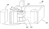
図1に示すように、半導体試験装置100は、土台1、Y方向の移送機構2、搬送台3、通電部4、冷却板5、プローブ6、加圧板7、サーボプレス8、支柱9、電源10、PLC11、画面12、プレスコントローラ13、電源コントローラ14、吸着パッド21、撮像部22、第一の照射部23、第二の照射部24、遮光壁25、検査部26、Z方向の移送機構27、及びX方向の移送機構28を備える。半導体試験装置100は、大電流を流す用途で用いられる半導体素子15の電気的特性を評価するために用いられる装置である。
As shown in FIG. 1, the
土台1には、半導体素子の通電試験を行うための搬送台3、プローブ6、加圧板7、サーボプレス8、及び支柱9が備えられている。搬送台3上に、通電加圧の対象となる通電部4が搭載されている。また、通電試験後の搬送台3を検査部26に移送するためのX方向の移送機構28、Y方向の移送機構2、及びZ方向の移送機構27が備えられている。さらに、半導体素子15を吸着して検査部26に移送するための吸着パッド21が備えられている。X方向の移送機構28、Y方向の移送機構2、及びZ方向の移送機構27は、レールとブロックにより構成され、半導体素子を載せたブロックがレール上をスライドする機構として、例えばアクチュエータを用いる。半導体素子15は、上述の移送機構により通電部4から検査部26に向かって移送される。さらに、土台1には、半導体素子の検査部26が備えられている。なお、本件実施の形態では、土台1、搬送台3、及び支柱9は、アルミニウム部品を含む材質による構成としたが、耐久性と耐摩耗性を有する材質であればよく、例えば、鉄、ステンレス(SUS)、及びプラスチック等が用いられる。
The base 1 is provided with a
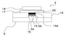
図2に示すように、通電部4は、半導体素子15の位置決めをするガイド19、ガイド19に設けられた穴19a、ガイド19の裏面に配置された冷却板5、冷却板5に設けられた凸部5a、半導体素子15と冷却板5との間に配置された第三の間材16、ガイド19に跨って半導体素子15を覆い配置された第二の間材17、及び第二の間材17の上に重ねて半導体素子15を覆い配置された第一の間材18を備える。
As shown in FIG. 2, the
半導体素子15は通電の対象物であり、少なくともその第一の主面である表面35と、表面35に対向する第二の主面である裏面36とに電極を有している。表面35には、微細な回路パターンが形成されている。半導体素子15として、例えば、炭化珪素を用いたショットキーバリアダイオードやMOSFET(Metal−Oxide−Semiconductor Field−Effect−Transistor)等が考えられる。
The
第一の間材18は、半導体素子15と同等以上の大きさであればよいが、耐久性の観点から厚みがある程好ましい。また第一の間材18は、プローブ6と接触する部分を有するため、プローブ6と半導体素子15との接触面積を増やすために、研磨されることにより面粗さを小さくすることが好ましい。さらに第一の間材18は、下降したプローブ6の底面と半導体素子15との平行度のずれを吸収し、両者間の平行度を良好にする役割を有している。特に、複数本から成るプローブ6を用いた場合には、プローブ6の長さにバラつきが生じるため、加圧力を均一にするためには第一の間材18に一定の厚みが必要となる。第一の間材18が薄いと塑性変形しやすいことから、加圧力の均一化に劣りが生じて、素子の破損や局所的な電流集中が起きやすくなり、半導体素子15に酸化膜による変色が発生しやすくなる。
The first
第二の間材17は、半導体素子15を覆うことのできる大きさであればよいが、厚さに関しては、半導体素子15の表面35に形成されている電極パターン等の数μmある段差を吸収する程度の厚みが必要である。第二の間材17の厚みが十分ではないと、通電試験中にアルミニウム製の間材又は冷却板が破断し、通電試験が失敗してしまう場合がある。また、第二の間材17の厚みが大きすぎる場合、通電加圧時の発熱により圧延方向に熱膨張が大きくなり、半導体素子15の熱膨張との差により半導体素子15に傷が発生しやすくなる。また、剛性が高くなることで加圧時に半導体素子15の面の形状にあわせた変形により空隙ができてしまい、放熱性が悪化することで半導体素子15の裏面36に酸化膜による変色が発生しやすくなる。
The second
第二の間材17は、第三の間材16と接続された極とは反対側の極に第一の間材18を介して接続されており、電源10から半導体素子15への通電のため、半導体素子15の表面35の電極に接触する。
The second
第三の間材16は、半導体素子15の裏面36の電極に接触しており、この半導体素子15の裏面36の電極と電源10とが接続されている。つまり、第三の間材16は、冷却板5を介して、電源10の正極または負極と接続されている。
The third
第一の間材18、第二の間材17、及び第三の間材16の材質としては、電気伝導度が高く、耐熱性を有し、耐摩耗性を有する物質であればよく、例えば、銅やアルミニウム等が用いられる。
The material of the first
冷却板5は、半導体素子15の裏面36側に設けられ、半導体試験装置100が通電試験を行なう際に発熱した半導体素子15を冷却させるための部材である。冷却板5は、矩形の平面形状を有する板状の部材であり、第三の間材16を介して半導体素子15を載置している。ガイド19により位置決めされた半導体素子15に生じる通電時の発熱は、第三の間材16を介して冷却板5の中央部に設けられた凸部5aを伝わって冷却される。冷却板5は、導電性と熱伝導性が高く、耐熱性と耐摩耗性を有する物質であればよく、例えば、銅、アルミニウム、及びカーボン等が用いられる。
The
プローブ6は、第一の間材18と接触することにより、半導体素子15に大電流を流し、半導体素子15からの応答信号を取得するために、第一の間材18の上に配置されている。プローブ6は、例えば、Z方向に沿って延びるように加圧板7に固定され、円筒形状を有している。プローブ6は、一般的にタングステン等の炭素工具鋼により形成されているが、プローブ6を構成する材質はこれに限られない。プローブ6は、導電性が高く、耐熱性と耐摩耗性を有し、且つ加圧するために一定の耐荷重を有する物質であればよく、例えば、ジェラコン、真鍮、ステンレス等を用いてもよい。プローブ6は、一本あたりの荷重と電流密度に耐えることができれば、一本で通電加圧してもよいし、又は複数本で通電加圧してもよい。
The
また、加圧板7を構成する材質についても同様で、炭素工具鋼により形成されていることが好ましいが、加圧板7を構成する材質はこれに限られない。加圧板7は、プローブ6への電気的な接続と、発熱したプローブ6を冷却するために、導電性が高く、耐熱性と耐摩耗性を有する物質であればよく、例えば、銅やアルミニウム等を用いてもよい。
The same applies to the material constituting the pressure plate 7, and it is preferable that the material is made of carbon tool steel, but the material constituting the pressure plate 7 is not limited to this. The pressure plate 7 may be a substance having high conductivity, heat resistance and abrasion resistance in order to electrically connect to the
ガイド19には、半導体素子15と第三の間材16の位置決めをするための穴19aが設けられている。ガイド19を構成する材質としては、半導体素子15への通電が分流しないようにするため、絶縁性、耐熱性、及び耐摩耗性を有する物質であればよく、例えば、銅やアルミニウム等が用いられる。なお、ガイド19は、セラミック系の高分子材料に限るわけではなく、金属材料を絶縁コーティングしたものを用いてもよい。例えば、金属材料に絶縁テープを巻いたものや、セラミックコーティング、及びガラスコーティング等をしたものが挙げられる。これにより、安価に、電流の分流等、通電試験のプロセスに悪影響を及ぼす原因を低減することができる。
The
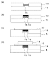
次に、このように構成された半導体検査装置における半導体素子の通電試験について、図1、図3、及び図4を用いて説明する。 Next, the energization test of the semiconductor element in the semiconductor inspection apparatus configured as described above will be described with reference to FIGS. 1, 3, and 4.
図3は、通電試験の動作を示す図である。まず図3(a)に示すように、冷却板5上において、第三の間材16がガイド19により位置決めをされて配置される。次に図3(b)に示すように、第三の間材16の上に半導体素子15が配置される。続いて図3(c)
に示すように、ガイド19に跨って半導体素子15を覆うように第二の間材17が配置される。さらに、図3(d)に示すように、第二の間材17の上に重ねて半導体素子15を覆うように第一の間材18が配置される。
FIG. 3 is a diagram showing the operation of the energization test. First, as shown in FIG. 3A, the third
As shown in the above, the second
図1に示すように、半導体試験装置100は、搬送台3上に通電部4を搭載した状態で、アクチュエータ等で構成されたY方向の移送機構2により、サーボプレス8の下、つまり加圧板7とプローブ6の下まで、搬送台3の移送を可能とする。搬送台3を移送させる場合は、操作をするための画面12として、例えばGOT(Graphic Operation Terminal)(登録商標)を用いる。画面12における搬送台3を移送させるための指示情報は、PLC(Programmable Logic Controller)11においてY方向の移送機構2の制御信号に変換され、Y方向の移送機構2により搬送台3が移送される。
As shown in FIG. 1, the
図4は、通電試験の動作を示す図である。図4(a)に示すように、最初、プローブ6は通電部4に配置された第一の間材18に接触していない。次に、図4(b)に示すように、PLC11からの制御情報により、プレスコントローラ13にて予め設定している条件を読み込むことで、支柱9に支えられたサーボプレス8が加圧板7を搬送台3上の通電部4に向けて下降し、プローブ6は通電部4に配置された第一の間材18と接触する。その後、PLC11からの指示により、プローブ6の加圧力を任意に設定した規定の荷重値(25kg〜100kg)まで上昇させた後、電源コントローラ14にて予め設定している条件を読み込むことで、電源10から任意に設定した電流(電流密度が120[A/cm2]以上400[A/cm2]未満)を通電部4に対して継続して流す。その際、半導体素子15の温度は、150℃以上230℃以下とする。
FIG. 4 is a diagram showing the operation of the energization test. As shown in FIG. 4A, initially the
半導体試験装置100は、PLC11により、通電加圧中の半導体素子15の温度を冷却板5の凸部5aに取り付けた熱電対を用いて常時監視を行い、規定の温度(150℃以上230℃以下)から外れた場合には、PLC11により、通電加圧を停止する信号を、プレスコントローラ13と電源コントローラ14へ送信し、通電加圧を停止させる機能を有する。
The
また、半導体試験装置100において、電流密度が120[A/cm2]以上400[A/cm2]未満の範囲外の場合には、電源コントローラ14で通電加圧中の半導体素子15を不良品として判定する。判定結果はPLC11に送信され、PLC11により通電加圧を停止する信号がプレスコントローラ13と電源コントローラ14へ送信され、通電加圧を停止させる機能を有する。通電加圧を異常発生時に停止させる機能により、周辺機構へのダメージを抑制することができる。
Further, in the
続いて、通電後の半導体素子15の裏面36において、酸化膜による変色を検出する方法について、図5と図6を用いて説明する。
Subsequently, a method of detecting discoloration due to the oxide film on the back surface 36 of the
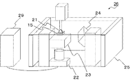
図5は、半導体検査装置の検査部の断面図である。図5に示すように、検査部26は、半導体素子15の表面35を吸着するための吸着パッド21、半導体素子15の裏面36に対向する撮像部22、第一の照射部23、第二の照射部24、遮光壁25、及び画像処理部29を備える。まず、吸着パッド21が半導体素子15を吸着する。吸着状態を維持したまま、持ち上げて中空で停止している半導体素子15の裏面36は、遮光壁25により外乱光の影響を遮蔽しておく。なお、遮光壁25は、暗幕等で代用することも可能である。
FIG. 5 is a cross-sectional view of an inspection unit of the semiconductor inspection apparatus. As shown in FIG. 5, the
次に、第一の波長の光を含む第一の照射部23と第二の波長の光を含む第二の照射部24とを、半導体素子15に向けて同時に照射する。第一の波長の光は、380nm未満の波長域の光を支配的に含む光であり、例えば紫外光(UV光)又は遠紫外光(DUV光)である。また、第二の波長の光は、380nm以上780nm未満の波長域の光を支配的に含む光であり、例えば可視光である。第一の照射部23は撮像部22と半導体素子15との間から半導体素子15を照射し、第二の照射部24は第一の波長を含む光とは異なる斜め方向から半導体素子15を照射する。第一の照射部23は、撮像部22と半導体素子15との間から半導体素子15を照射すればよく、例えば、撮像部22と半導体素子15との間にハーフミラーを設置し、このハーフミラーを介して光を照射する同軸照明装置を用いる。なお、ハーフミラーに替えて、ビームスプリッター等の光束を分岐できる分岐光学素子を用いてもよい。
Next, the
第一の照射部23と第二の照射部24としては、例えば、LED照明により所望の波長の光を照射する。ただし、第一の照射部23と第二の照射部24は、これに限定されるものではない。例えば、白色LED照明とカラーフィルタとの組み合わせによって構成してもよく、白色電球又は蛍光管とカラーフィルタとの組み合わせ、又はカラーランプ等を用いることもできる。また、第二の照射部24は、酸化膜領域31や傷領域32の特徴に応じて、適宜赤色、緑色、及び青色等の特定の波長の光を用いることもできる。特定の波長の光を用いることにより、酸化膜領域31や傷領域32からの反射光が強調されるため、上述の領域を検出する精度を高めることができる。
The
検査部26に配置されている撮像部22を用いて、半導体素子15の裏面36を撮像する。撮像部22の分光感度特性は、可視光波長域の感度が紫外光波長域の感度よりも高い。撮像部22は、第一の波長に基づく裏面36からの反射光と、第二の波長に基づく裏面36からの反射光とを含む裏面36からの反射光を撮像し、撮像により得られた画像データは、画像処理部29において取得される。第一の波長に基づく裏面36からの反射光は、正反射光を支配的に含む光である。また、第二の波長に基づく裏面36からの反射光は、拡散反射光を支配的に含む光である。なお、画像データとは、画像を構成する画素毎の明暗を示したデータのことをいう。
The back surface 36 of the
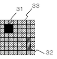
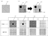
図6は、撮像により得られた画像データを示す図である。図6に示すように、画像データは、画像処理部29に備えられた判定部において、酸化膜領域31、傷領域32、及び正常領域33のうち、少なくともいずれかの領域に分割される。酸化膜領域31は、半導体素子15に発生した酸化膜による変色を示す領域である。傷領域32は、凹みや窪みを含む傷を示す領域である。正常領域33は、酸化膜領域31と傷領域32以外の領域を示し、半導体素子15において凹凸のない平坦な形状の領域である。
FIG. 6 is a diagram showing image data obtained by imaging. As shown in FIG. 6, the image data is divided into at least one of the
画像処理部29に備えられた判定部は、得られた画像データの特徴量に基づき、酸化膜領域31、傷領域32、及び正常領域33のうち、少なくとも酸化膜領域31を識別し、半導体素子15の良否を判定する。画像領域の識別は、例えば、画像データの各画素のデータ値が、酸化膜の閾値内であれば酸化膜領域31、傷の閾値内であれば傷領域32、いずれの閾値外であれば正常領域33と識別する。なお、これらの閾値は、撮像部22、第一の照射部23、及び第二の照射部24の特性によって変わるため、あらかじめ撮像部や照明の特性を考慮した上で決定することが望ましい。識別結果に基づき、画像データに酸化膜領域31が含まれない場合は、半導体素子15が良品であると判定し、画像データに酸化膜領域31が含まれる場合は、半導体素子15が不良品であると判定する。
The determination unit provided in the
このように、得られた画像データから、酸化膜領域31、傷領域32、及び正常領域33に分割されるのは、下記の理由によると解される。撮像部22の分光感度特性は、紫外光波長域の感度が可視光波長域の感度よりも低いため、第一の照射部23を撮像部22と半導体素子15との間から照射し、撮像部22で半導体素子15の裏面36を撮像すると、正常領域33から酸化膜領域31と傷領域32とを含む領域を区別可能なコントラストの低い画像データが得られる。しかし、画像データのコントラストが低いため、酸化膜領域31と傷領域32とを区別することが困難である。
It is understood that the reason why the obtained image data is divided into the
その理由としては、第一の照射部23を半導体素子15の裏面36に向けて照射した場合、得られた画像データにおいて、半導体素子15の裏面36にある傷領域32は、乱反射により撮像部22に戻る明るさの情報が区別できる程に含まれないためである。また、第一の照射部23を半導体素子15の裏面36に向けて照射した場合、得られた画像データにおいて、半導体素子15の裏面36にある酸化膜領域31は、紫外光波長域の光の吸収率が傷領域32における紫外光波長域の光の吸収率よりも高いことにより、酸化膜領域31の明るさの情報が区別できる程得られないためである。したがって、傷領域32と酸化膜領域31のいずれの領域においても、明るさの情報が区別できる程得られないため、両者のコントラストが低くなってしまう。
The reason is that when the
得られた画像データのコントラストを高めるため、第一の照射部23による照射と同時に、第一の波長を含む光とは異なる斜め方向から第二の照射部24を半導体素子15に照射する。これにより、凹凸のある傷領域32に明るさの情報が追加される。しかしながら、半導体素子15において酸化膜は凹凸のない平坦な形状であり、第一の波長を含む光とは異なる斜め方向からの光は全反射して半導体素子15の対角側へ反射するため、酸化膜領域31には傷領域32程の明るさの情報は追加されない。したがって、第一の照射部23と第二の照射部24とを、半導体素子15に向けて同時に照射することで、画像データにおいて、傷領域32と酸化膜領域31との間には、コントラストが生じる。また、正常領域33は、凹凸のない平坦な形状であることから、傷の領域と酸化膜の領域よりも明るさの情報を得るため、傷領域32と酸化膜領域31とに対し、コントラストが得られる。これにより、酸化膜領域31、傷領域32、及び正常領域33を検出することができる。
In order to increase the contrast of the obtained image data, at the same time as the irradiation by the
検出結果に基づき、画像データに酸化膜領域31が含まれない場合は、半導体素子15が良品であると判定し、画像データに酸化膜領域31が含まれる場合は、半導体素子15が不良品であると判定する。判定結果は、PLC11に接続された処理回路を通じて画像信号に変換され、画面12に文字や画像によって示される。
Based on the detection result, if the image data does not include the
以上により、本構成を用いることで、第一の波長の光を含む第一の照射部23と第二の波長の光を含む第二の照射部24とから、半導体素子15に向けて同時に照射し、撮像により得られた画像から、各領域間のコントラストの違いを利用して、半導体素子15の酸化膜領域31のみを検出することができる。また、酸化膜領域31、傷領域32、及び正常領域を、それぞれ区別して検出することもできる。
Based on the above, by using this configuration, the
次に、半導体素子の裏面36にグラデーションが生じた場合の検査アルゴリズムについて、図7を用いて説明する。 Next, an inspection algorithm when a gradation is generated on the back surface 36 of the semiconductor element will be described with reference to FIG. 7.
図7は、半導体素子の検査アルゴリズムを示す図である。図7(a)は、半導体素子15を示す画像データである。図7(a)に示すように、半導体素子15の裏面36は研磨されているため、半導体素子15の裏面36の正常領域33にグラデーション34が生じることがある。グラデーション34の発生により、正常領域33を検出できない場合は、動的二値化処理を行うことで、正常領域33を検出する。
FIG. 7 is a diagram showing an inspection algorithm for a semiconductor element. FIG. 7A is image data showing the
図7(b)は、動的二値化処理前と動的二値化処理後の画像データの例である。図7(b)において、動的二値化処理後の画像データの方が、動的二値化処理前の画像データよりもコントラストが高いことを示している。 FIG. 7B is an example of image data before and after the dynamic binarization process. FIG. 7B shows that the image data after the dynamic binarization process has a higher contrast than the image data before the dynamic binarization process.
動的二値化処理について、以下に説明をする。本実施の形態1では、動的二値化閾値を、中心画素の周辺のM×N画素の平均画素値のうち一定の割合の値であると定義する。本実施の形態1では、中心画素の周辺の5×5画素を対象の範囲と設定し、一定の割合を平均画素値のうち80%であると設定する。なお、M×N画素のサイズは、グラデーション34の特徴を考慮した上で設定することが望ましい。また、周辺の画素の形状は、十字形、×印形、又は長方形等、グラデーション34の特徴を考慮した上で設定することが望ましい。
The dynamic binarization process will be described below. In the first embodiment, the dynamic binarization threshold value is defined as a value of a certain ratio of the average pixel value of the M × N pixels around the central pixel. In the first embodiment, 5 × 5 pixels around the center pixel are set as the target range, and a certain ratio is set to be 80% of the average pixel value. It is desirable that the size of the M × N pixel is set in consideration of the characteristics of the
図7(c)は動的二値化処理の第一の例を示す図であり、図7(d)は動的二値化処理の第二の例を示す図である。 FIG. 7C is a diagram showing a first example of the dynamic binarization process, and FIG. 7D is a diagram showing a second example of the dynamic binarization process.
図7(c)の左側に示すように、中心画素は酸化膜領域31を示しており、その画素値は20である。中心画素の周辺の5×5画素の平均画素値は243であり、動的二値化閾値は194となる。したがって、図7(c)の右側に示すように、中心画素とその周辺画素において、画素値が動的二値化閾値内である画素の画素値は0に変換し、画素値が動的二値化閾値外である画素の画素値は255に変換する。
As shown on the left side of FIG. 7C, the central pixel shows the
また、図7(d)の左側に示すように、中心画素とその周辺の5×5画素は正常領域33を示しており、それらの画素値は127である。中心画素の周辺の5×5画素の平均画素値は127であり、動的二値化閾値は102となる。したがって、図7(d)の右側に示すように、中心画素とその周辺画素において、全画素の画素値が動的二値化閾値外であるため、これらの画素の画素値を255に変換する。
Further, as shown on the left side of FIG. 7D, the central pixel and the 5 × 5 pixels around it indicate the
上記の動的二値化処理を行うことで、半導体素子15の裏面36の正常領域33に発生するグラデーション34による影響を抑制し、酸化膜領域31を安定して検出することができる。
By performing the above dynamic binarization process, the influence of the
このように、半導体素子15において、第一の照射部23、第二の照射部24、及びこれらの照明によって照射された半導体素子15からの反射光を撮像する撮像部22を備えることにより、酸化膜による変色を含む半導体素子15のみを不良品として判定することが可能となり、半導体素子15を検査する精度が上がるという効果を奏する。
As described above, the
また、半導体素子15と半導体素子15の外との境界付近で動的二値化処理を実施した場合、半導体素子15の外の画素値が半導体素子15の画素値よりも低くなることによって、正常領域33を誤って酸化膜領域31と検出してしまうことがある。これに対し、予め半導体素子15の形状をエッジ検出手法やパターンマッチング手法等により検出し、検査範囲を限定しておくことによって、誤検出を抑制することができる。
Further, when the dynamic binarization process is performed near the boundary between the
なお、本件発明の実施の形態1では、判定結果を画面12に文字や画像によって示していたが、スピーカから音声によって示してもよい。この場合、半導体試験装置100と画面12との距離が離れている環境においては、音声による情報提示が行えるという効果を奏する。
In the first embodiment of the present invention, the determination result is shown on the
さらに、本件発明の実施の形態1では、判定部において半導体素子15の良否を判定していたが、判定部に替えて、画像処理部29を介して少なくとも酸化膜領域31が識別された画像データを画面12に表示させてもよい。この場合、人が画面12に表示された画像データの酸化膜領域31に基づき、半導体素子15の良否を判定することによって、判定部における判定の処理に係る実装コストを抑制することができる。
Further, in the first embodiment of the present invention, the determination unit determines the quality of the
半導体素子15の検査において、検査部26での通電時間に対して検査時間は短いため、検査終了後に半導体素子15の判定結果に基づき、Z方向の移送機構27とX方向の移送機構28を用いて、半導体素子15の良品と不良品をそれぞれ良品トレイと不良品トレイ等に載せて搬送してもよい。同様にして、Z方向の移送機構27とX方向の移送機構28を用いて、半導体素子15、第一の間材18、第二の間材17、及び第三の間材16をそれぞれ搬送台3に載せて搬送してもよい。これにより、半導体素子15の検査を人の手に依らずに行なうため、検査時間を短縮することができる。
In the inspection of the
また、土台1に撮像部22を搭載しておくことにより、半導体素子15の裏面36を検査する際に半導体素子15を反転するための機構を必要とすることなく、通電試験中に半導体素子15の検査を実施することができる。
Further, by mounting the
実施の形態2.
本件発明の実施の形態2における半導体検査装置について、図8を用いて説明する。なお、図8において、図5と同一符号は同一又は相当部分を示す。
The semiconductor inspection apparatus according to the second embodiment of the present invention will be described with reference to FIG. In FIG. 8, the same reference numerals as those in FIG. 5 indicate the same or corresponding portions.
本件実施の形態1において、第二の照射部24は、第一の波長を含む光とは異なる斜め方向から半導体素子15を照射する構成にしたが、例えば、半導体素子15の周囲の方向から照射する照射部により構成してもよい。図8は、本件実施の形態2における半導体検査装置の検査部の断面図である。第二の照射部24の代わりにリング照明30を用いることにより、第二の照射部24よりも広い範囲から半導体素子15を照射している。
In the first embodiment, the
この構成にすることによって、傷領域32からの反射光は、第二の照射部24からの照射光よりも明るくなる。一方で、酸化膜領域31は凹凸がなく平坦な形状のため、酸化膜領域31からの反射光は、第二の照射部24からの照射光よりも暗くなる。その結果、撮像によってコントラストの高い画像データが得られ、これらの領域の検出精度を高めることができる効果を奏する。なお、広い範囲から半導体素子15を照射するための照明としては、必要とされる照射範囲に応じて、リング照明30の代わりにドーム照明等、適宜最適なものを用いてもよいことは言うまでもない。
With this configuration, the reflected light from the scratched
なお、以上の実施形態は、本発明を具体化した一例であって、本発明の技術的範囲を限定するものではない。 The above embodiment is an example embodying the present invention, and does not limit the technical scope of the present invention.
1 土台、2 Y方向の移送機構、3 搬送台、4 通電部、5 冷却板、5a 凸部、6 プローブ、7 加圧板、8 サーボプレス、9 支柱、10 電源、11 PLC、12 画面、13 プレスコントローラ、14 電源コントローラ、15 半導体素子、16 第三の間材、17 第二の間材、18 第一の間材、19 ガイド、19a 穴、21 吸着パッド、22 撮像部、23 第一の照射部、24 第二の照射部、25 遮光壁、26 検査部、27 Z方向の移送機構、28 X方向の移送機構、29 画像処理部、30 リング照明、31 酸化膜領域、32傷領域 、33正常領域 、34 グラデーション、35 表面、36 裏面、100 半導体試験装置 1 base, 2 Y-direction transfer mechanism, 3 transport base, 4 current-carrying part, 5 cooling plate, 5a convex part, 6 probe, 7 pressure plate, 8 servo press, 9 columns, 10 power supply, 11 PLC, 12 screens, 13 Press controller, 14 power controller, 15 semiconductor element, 16 third interleaving material, 17 second interleaving material, 18 first interleaving material, 19 guide, 19a hole, 21 suction pad, 22 image pickup unit, 23 first Irradiation part, 24 second irradiation part, 25 shading wall, 26 inspection part, 27 Z direction transfer mechanism, 28 X direction transfer mechanism, 29 image processing part, 30 ring illumination, 31 oxide film area, 32 scratch area, 33 Normal region, 34 Gradation, 35 Front surface, 36 Back surface, 100 Semiconductor test equipment
Claims (6)
前記面に対向する位置に設けられた撮像部と、
前記面と前記撮像部との間に設けられ、第一の波長を含む光を前記面に照射する第一の照射部と、
前記第一の波長を含む光とは異なる方向から、前記第一の波長とは異なる第二の波長を含む光を前記面に照射する第二の照射部と、
前記第一の波長に基づく前記面からの反射光と、前記第二の波長に基づく前記面からの反射光と、を含む反射光による画像データを取得し、取得した前記画像データのコントラストの高さに基づいて、前記画像データのうちから前記酸化膜による変色を示す画像領域である酸化膜領域を識別する画像処理部と
を備える半導体検査装置。 In a semiconductor inspection device that inspects whether or not there is discoloration due to an oxide film on the surface of a semiconductor element after energization.
An imaging unit provided at a position facing the surface and
A first irradiation unit provided between the surface and the imaging unit and irradiating the surface with light containing a first wavelength,
A second irradiation unit that irradiates the surface with light containing a second wavelength different from the first wavelength from a direction different from the light containing the first wavelength.
Image data by reflected light including the reflected light from the surface based on the first wavelength and the reflected light from the surface based on the second wavelength is acquired, and the contrast of the acquired image data is high. based at the semiconductor inspection device and an image processing unit to identify the oxide region is an image region that shows a color change due to the oxide film from among the image data.
請求項1に記載の半導体検査装置。 The semiconductor inspection apparatus according to claim 1, wherein the first wavelength is less than 380 nm.
請求項1に記載の半導体検査装置。 The semiconductor inspection apparatus according to claim 1, wherein the second wavelength is 380 nm or more and less than 780 nm.
請求項1から請求項3のいずれか1項に記載の半導体検査装置。 The semiconductor inspection apparatus according to any one of claims 1 to 3, wherein the spectral sensitivity characteristic of the imaging unit is such that the sensitivity of the second wavelength is higher than the sensitivity of the first wavelength.
請求項1から請求項4のいずれか1項に記載の半導体検査装置。 The semiconductor inspection apparatus according to any one of claims 1 to 4, wherein the image data is divided into at least two or more image regions including the oxide film region based on the height of contrast.
前記面と撮像部との間から、第一の波長を含む光を前記面に照射する工程と、
前記第一の波長を含む光とは異なる方向から、前記第一の波長とは異なる第二の波長を含む光を前記面に照射する工程と、
前記第一の波長に基づく前記面からの反射光と、前記第二の波長に基づく前記面からの反射光と、を含む反射光による画像データを取得し、取得した前記画像データのコントラストの高さに基づいて、前記画像データのうちから前記酸化膜による変色を示す画像領域である酸化膜領域を識別する工程と
を含む半導体検査方法。 It is a semiconductor inspection method that inspects whether or not the surface of a semiconductor element after energization is discolored by an oxide film.
From between the surface and the imaging unit, and a step of irradiating light including a first wavelength to said surface,
A step of irradiating the surface with light containing a second wavelength different from the first wavelength from a direction different from the light containing the first wavelength.
Image data by reflected light including the reflected light from the surface based on the first wavelength and the reflected light from the surface based on the second wavelength is acquired, and the contrast of the acquired image data is high. based at the semiconductor inspection method comprising a step of identifying the oxide region is an image region that shows a color change due to the oxide film from among the image data.
Priority Applications (1)
| Application Number | Priority Date | Filing Date | Title |
|---|---|---|---|
| JP2017062041A JP6906339B2 (en) | 2017-03-28 | 2017-03-28 | Semiconductor inspection equipment and semiconductor inspection method |
Applications Claiming Priority (1)
| Application Number | Priority Date | Filing Date | Title |
|---|---|---|---|
| JP2017062041A JP6906339B2 (en) | 2017-03-28 | 2017-03-28 | Semiconductor inspection equipment and semiconductor inspection method |
Publications (2)
| Publication Number | Publication Date |
|---|---|
| JP2018165616A JP2018165616A (en) | 2018-10-25 |
| JP6906339B2 true JP6906339B2 (en) | 2021-07-21 |
Family
ID=63922789
Family Applications (1)
| Application Number | Title | Priority Date | Filing Date |
|---|---|---|---|
| JP2017062041A Active JP6906339B2 (en) | 2017-03-28 | 2017-03-28 | Semiconductor inspection equipment and semiconductor inspection method |
Country Status (1)
| Country | Link |
|---|---|
| JP (1) | JP6906339B2 (en) |
Family Cites Families (5)
| Publication number | Priority date | Publication date | Assignee | Title |
|---|---|---|---|---|
| JPS6238348A (en) * | 1985-08-14 | 1987-02-19 | Mitsubishi Metal Corp | Optical inspecting method for surface defect |
| JP4121735B2 (en) * | 2001-01-22 | 2008-07-23 | ソニー株式会社 | Polysilicon film evaluation system |
| US7206442B1 (en) * | 2001-11-16 | 2007-04-17 | Rudolph Technologies, Inc. | Optical inspection method utilizing ultraviolet light |
| JP6004033B1 (en) * | 2015-04-14 | 2016-10-05 | 株式会社Sumco | Epitaxial wafer evaluation method and evaluation apparatus |
| JP6394514B2 (en) * | 2015-06-25 | 2018-09-26 | Jfeスチール株式会社 | Surface defect detection method, surface defect detection apparatus, and steel material manufacturing method |
-
2017
- 2017-03-28 JP JP2017062041A patent/JP6906339B2/en active Active
Also Published As
| Publication number | Publication date |
|---|---|
| JP2018165616A (en) | 2018-10-25 |
Similar Documents
| Publication | Publication Date | Title |
|---|---|---|
| JP6042402B2 (en) | Illumination module and visual inspection system using the same | |
| JP5078583B2 (en) | Macro inspection device and macro inspection method | |
| US7027640B2 (en) | Method and apparatus for inspecting defects on polishing pads to be used with chemical mechanical polishing apparatus | |
| JP5854531B2 (en) | Printed circuit board inspection equipment | |
| JP5077872B2 (en) | Defect inspection apparatus and method by photoluminescence of solar cell | |
| US7852982B2 (en) | Test method | |
| US8330948B2 (en) | Semiconductor test instrument and the method to test semiconductor | |
| US8467062B2 (en) | Inspection device and producing method of wired circuit board | |
| JP2006112845A (en) | Pattern inspection device | |
| JP5830229B2 (en) | Wafer defect inspection system | |
| JP6483022B2 (en) | Thin section sample evaluation apparatus, thin section sample preparation apparatus including the thin section sample evaluation apparatus, and thin section sample evaluation method | |
| JP6908123B2 (en) | Visual inspection equipment and visual inspection method | |
| JP6906339B2 (en) | Semiconductor inspection equipment and semiconductor inspection method | |
| JP2009109243A (en) | Resin sealing material inspection equipment | |
| KR20130130567A (en) | Apparatus for inspecting of led and led inspection method using the same | |
| JP5787668B2 (en) | Defect detection device | |
| TW200538716A (en) | Method for inspecting insulating film for film carrier tape for mounting electronic components thereon, inspection apparatus for inspecting the insulating film, punching apparatus for punching the insulating film, and method for controlling the punching | |
| JP2011106912A (en) | Imaging illumination means and pattern inspection device | |
| JP2006292412A (en) | Surface inspection system, surface inspection method and substrate manufacturing method | |
| JP5100371B2 (en) | Foreign matter inspection method and foreign matter inspection apparatus for wafer peripheral edge | |
| JP7271329B2 (en) | Lighting device and visual inspection device equipped with the same | |
| TW202412132A (en) | Inspection equipment and inspection methods | |
| CN100504363C (en) | Inspection apparatus, inspection method, inspection apparatus, inspection method of wiring pattern | |
| JP2005077272A (en) | Method for inspecting defect | |
| KR200336984Y1 (en) | A device for inspecting surface and shape of an object of examination |
Legal Events
| Date | Code | Title | Description |
|---|---|---|---|
| A621 | Written request for application examination |
Free format text: JAPANESE INTERMEDIATE CODE: A621 Effective date: 20190909 |
|
| A977 | Report on retrieval |
Free format text: JAPANESE INTERMEDIATE CODE: A971007 Effective date: 20200630 |
|
| A131 | Notification of reasons for refusal |
Free format text: JAPANESE INTERMEDIATE CODE: A131 Effective date: 20201027 |
|
| RD01 | Notification of change of attorney |
Free format text: JAPANESE INTERMEDIATE CODE: A7421 Effective date: 20201106 |
|
| A521 | Request for written amendment filed |
Free format text: JAPANESE INTERMEDIATE CODE: A523 Effective date: 20201218 |
|
| TRDD | Decision of grant or rejection written | ||
| A01 | Written decision to grant a patent or to grant a registration (utility model) |
Free format text: JAPANESE INTERMEDIATE CODE: A01 Effective date: 20210601 |
|
| A61 | First payment of annual fees (during grant procedure) |
Free format text: JAPANESE INTERMEDIATE CODE: A61 Effective date: 20210629 |
|
| R150 | Certificate of patent or registration of utility model |
Ref document number: 6906339 Country of ref document: JP Free format text: JAPANESE INTERMEDIATE CODE: R150 |
|
| R250 | Receipt of annual fees |
Free format text: JAPANESE INTERMEDIATE CODE: R250 |
|
| R250 | Receipt of annual fees |
Free format text: JAPANESE INTERMEDIATE CODE: R250 |