JP2011106912A - Imaging illumination means and pattern inspection device - Google Patents
Imaging illumination means and pattern inspection device Download PDFInfo
- Publication number
- JP2011106912A JP2011106912A JP2009260885A JP2009260885A JP2011106912A JP 2011106912 A JP2011106912 A JP 2011106912A JP 2009260885 A JP2009260885 A JP 2009260885A JP 2009260885 A JP2009260885 A JP 2009260885A JP 2011106912 A JP2011106912 A JP 2011106912A
- Authority
- JP
- Japan
- Prior art keywords
- light
- illumination
- imaging
- half mirror
- pattern
- Prior art date
- Legal status (The legal status is an assumption and is not a legal conclusion. Google has not performed a legal analysis and makes no representation as to the accuracy of the status listed.)
- Pending
Links
Images
Landscapes
- Investigating Materials By The Use Of Optical Means Adapted For Particular Applications (AREA)
Abstract
【課題】同軸照明を使った撮像照明手段において、明るい画像が撮像素子に取り込まれるようにするとともに、線幅の細くなっている部分を明瞭に撮像できるようにすること。
【解決手段】光源100から出射した照明光は拡散板101を介してハーフミラー(ペリクル)110に入射し一部の光が反射されて基板W(被照明物)を照明する。基板Wで反射した光の一部はハーフミラー110を通過して撮像手段120の撮像素子121に入射し、基板Wに形成されたパターン像が撮像される。ハーフミラー110の、撮像対象(撮像領域)の像が通過する部分の外側であって照明光が入射する側に、被照明物に向かって照明光を全反射する反射部材(ミラー)130が取り付けられている。光源100からの照明光は、上記ハーフミラー110で反射するとともに、この反射部材130で反射して基板Wに照射される。このため、基板W(被照明物)を明るく照明することができる。
【選択図】 図1In an imaging illumination unit using coaxial illumination, a bright image is captured by an imaging element, and a portion with a narrow line width can be clearly imaged.
Illumination light emitted from a light source 100 enters a half mirror (pellicle) 110 via a diffuser plate 101, and a part of the light is reflected to illuminate a substrate W (object to be illuminated). Part of the light reflected by the substrate W passes through the half mirror 110 and enters the image sensor 121 of the imaging unit 120, and a pattern image formed on the substrate W is captured. A reflection member (mirror) 130 that totally reflects the illumination light toward the object to be illuminated is attached to the outside of the portion of the half mirror 110 where the image of the imaging target (imaging region) passes and is incident on the illumination light. It has been. The illumination light from the light source 100 is reflected by the half mirror 110 and is reflected by the reflecting member 130 and applied to the substrate W. For this reason, the substrate W (object to be illuminated) can be illuminated brightly.
[Selection] Figure 1
Description
本発明は、被照明物(対象物)を同軸照明により照明し撮像する撮像照明手段およびこの撮像照明手段を用いたパターン検査装置に関し、特に、プリント配線基板等の基板に形成された配線等のパターンの線幅や形状の検査に用いられる撮像照明手段およびパターン検査装置に関するものである。 The present invention relates to an imaging illuminating means for illuminating an object to be illuminated (object) with coaxial illumination, and a pattern inspection apparatus using the imaging illuminating means, and more particularly to a wiring formed on a substrate such as a printed wiring board. The present invention relates to an imaging illumination unit and a pattern inspection apparatus used for inspection of a line width and shape of a pattern.
プリント配線基板等の基板に形成された配線等のパターンの線幅を検査するパターン検査装置においては、パターンが形成された基板に対して照明光を照射し、照明されたパターン像を撮像素子により撮像し、撮像した画像を、例えば良品のサンプル画像と比較して、形成したパターンの良否を判定することが行われる。
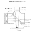
この、基板を照明して撮像する手段の一つに同軸照明と呼ばれる方法がある。同軸照明は、照明光が照射されている方向と同じ方向から撮像する方法である。図7に、同軸照明を使った従来の撮像照明手段の構成例を示す。
図7(a)は、同軸照明の撮像照明手段の断面図である。
撮像照明手段は、大まかには、照明光を出射する光源100と、光源100からの照明光を被照明物に向かつて反射するハーフミラー110と、ハーフミラー110に対して被照明物とは反対側に配置された撮像手段120とを備える。
100は照明光を出射する光源であり、同図においては、平面状に複数配置されたLEDである。光源100の光出射側には拡散板101が配置され、光源の光強度のムラを少なくする。拡散板101により拡散された光は、斜めに配置されたハーフミラー110に入射する。
In a pattern inspection apparatus that inspects the line width of a pattern such as a wiring formed on a substrate such as a printed wiring board, illumination light is irradiated to the substrate on which the pattern is formed, and the illuminated pattern image is captured by an image sensor. An image is picked up, and the picked-up image is compared with, for example, a good sample image to determine whether the formed pattern is good or bad.
One of the means for illuminating the substrate to take an image is a method called coaxial illumination. Coaxial illumination is a method of imaging from the same direction as the direction in which illumination light is irradiated. FIG. 7 shows a configuration example of conventional imaging illumination means using coaxial illumination.
FIG. 7A is a cross-sectional view of the imaging illumination means for coaxial illumination.
The imaging illuminating means roughly includes a light source 100 that emits illumination light, a half mirror 110 that reflects the illumination light from the light source 100 toward the object to be illuminated, and the half mirror 110 opposite to the object to be illuminated. And imaging means 120 disposed on the side.
Reference numeral 100 denotes a light source that emits illumination light. In the figure, a plurality of LEDs are arranged in a planar shape. A diffusion plate 101 is disposed on the light emitting side of the light source 100 to reduce unevenness in the light intensity of the light source. The light diffused by the diffusing plate 101 enters the half mirror 110 disposed obliquely.
本例においては、ハーフミラー110としてペリクルと呼ばれる半透過性の薄膜を使用している。ハーフミラー(ペリクル)110は、透過光と反射光の比率を任意に設定できるが、ここでは、例えば入射する光のうち50%の光が反射し50%の光が透過するものとする。したがって、入射した光のうち50%が反射され、ハーフミラー110の下方に置かれた、パターンを形成した基板(撮像対象)Wの表面を照明する。
上記したように、光源100からの光は拡散板101により拡散されており、ハーフミラー(ペリクル)110には、様々な入射角度の光が入射する。したがって、ハーフミラー(ペリクル)110による反射光も様々な角度であり、基板Wは様々な入射角度の光により照明される。同図において、光源から出射した照明光を、点線の矢印で示している。
基板Wの表面に照射された照明光は、形成されているパターンや基板表面で反射され、再びハーフミラー110に入射する。ハーフミラー110に入射した光は、50%は光源100の方向に反射されるが、50%は撮像手段120に入射する。これにより照明光により照明されたパターン像が撮像される。撮像手段120は内部にCCDセンサなどの撮像素子121を備える。Sは、撮像素子121が撮像する領域(撮像領域)である。
このような撮像照明手段を用いて、例えば、樹脂製のプリント基板上に形成された金属の配線パターンを観察すると、金属の配線パターンと樹脂製の基板とでは照明光の反射率が異なるので、撮像素子121には配線パターンがくっきりと映し出され、パターンの線幅の測定を容易に行うことができる。
In this example, a semi-transmissive thin film called a pellicle is used as the half mirror 110. The half mirror (pellicle) 110 can arbitrarily set the ratio of transmitted light and reflected light, but here, for example, 50% of incident light is reflected and 50% of light is transmitted. Therefore, 50% of the incident light is reflected and illuminates the surface of the substrate (imaging target) W on which the pattern is placed, which is placed below the half mirror 110.
As described above, the light from the light source 100 is diffused by the diffusion plate 101, and light having various incident angles enters the half mirror (pellicle) 110. Therefore, the reflected light from the half mirror (pellicle) 110 also has various angles, and the substrate W is illuminated with light having various incident angles. In the figure, illumination light emitted from the light source is indicated by a dotted arrow.
The illumination light applied to the surface of the substrate W is reflected by the formed pattern and the substrate surface, and is incident on the half mirror 110 again. 50% of the light incident on the half mirror 110 is reflected in the direction of the light source 100, but 50% is incident on the imaging unit 120. Thereby, the pattern image illuminated with illumination light is imaged. The imaging unit 120 includes an imaging element 121 such as a CCD sensor. S is an area (imaging area) where the image sensor 121 captures an image.
Using such an imaging illumination means, for example, when observing a metal wiring pattern formed on a resin printed board, the reflectance of illumination light differs between the metal wiring pattern and the resin board. A wiring pattern is clearly displayed on the image sensor 121, and the line width of the pattern can be easily measured.
図7(b)は、ハーフミラーであるペリクル110とその保持手段(フレーム)111を、照明光が入射する側から見た図である。ペリクル110は、半透過性の薄膜であり市販されている。露光装置のフォトマスクの保護膜として使用されることが多いが、透過する光の量と反射する光量の比を設定できることもあり、ハーフミラーとしても使用される。ペリクル110は、周辺部をフレームによってたわまないように挟まれて支持され、フレーム111はとめねじ112等で固定される。
このような同軸照明を使った撮像照明手段は、例えば特許文献1に記載されたパターン検査装置の、反射照明手段31として使用されている。
FIG. 7B is a view of the pellicle 110 that is a half mirror and its holding means (frame) 111 as viewed from the side on which the illumination light is incident. The pellicle 110 is a semi-permeable thin film and is commercially available. Although it is often used as a protective film for a photomask of an exposure apparatus, the ratio between the amount of transmitted light and the amount of reflected light can be set, and it is also used as a half mirror. The pellicle 110 is supported by being sandwiched so that the peripheral portion is not bent by the frame, and the frame 111 is fixed by a female screw 112 or the like.
Such imaging illumination means using coaxial illumination is used as the reflection illumination means 31 of the pattern inspection apparatus described in Patent Document 1, for example.
同軸照明を使った撮像照明手段においては、上記したように、撮像対象を照明する照明光は、ハーフミラー(ペリクル)110に反射した光である。そのため、ハーフミラー(ペリクル)110の透過率と反射率が50:50であれば、撮像対象を照明する明るさは、光源100から出射する光の明るさに比べると半分になる。また、照明された撮像対象の画像も、ハーフミラー(ペリクル)110を介して撮像素子121に取り込まれる。そのため、画像の明るさはさらに半分になる。
したがって、撮像素子121に入射する光の明るさは、光源100から出射する照明光の明るさから比べると1/4からそれ以下となり、撮像素子121が取り込む画像は暗くなりがちである。そのため、撮像対象(基板W)に形成されているパターンの反射率が低い場合、基板とパターンのコントラストが悪くなり、パターンを検出することが難しくなる。
In the imaging illumination means using coaxial illumination, as described above, the illumination light that illuminates the imaging target is light reflected by the half mirror (pellicle) 110. Therefore, if the transmittance and reflectance of the half mirror (pellicle) 110 are 50:50, the brightness for illuminating the imaging target is half that of the light emitted from the light source 100. The illuminated image to be captured is also captured by the image sensor 121 via the half mirror (pellicle) 110. Therefore, the brightness of the image is further halved.
Therefore, the brightness of the light incident on the image sensor 121 is ¼ to less than the brightness of the illumination light emitted from the light source 100, and the image captured by the image sensor 121 tends to be dark. Therefore, when the reflectance of the pattern formed on the imaging target (substrate W) is low, the contrast between the substrate and the pattern is deteriorated, and it is difficult to detect the pattern.
この問題を解決するために、例えば、反射率の大きいハーフミラー(ペリクル)110を使用することも考えられる。そのようにすると、ハーフミラー(ペリクル)110により反射される照明光の量が多くなるので、撮像対象の照度は明るくなる。しかし、ハーフミラー(ペリクル)110は、反射率を高くした分透過率が低くなる(反射率を80%にすると透過率は20%になる)ので、撮像領域の画像がハーフミラー(ペリクル)110を通過しにくくなり、やはり撮像素子に取り込まれる画像は暗くなる。
また、照明光源100であるLEDのパワーを大きくすれば照度は明るくなる。しかし、LEDのパワーが大きくなると、その分LEDの発熱量も大きくなり、冷却手段が必要となると共に、LEDの寿命も短くなる。そのため、LEDのパワーを上げることなく効率よく照明を行い、画像を明るくすることが望まれている。
In order to solve this problem, for example, it is conceivable to use a half mirror (pellicle) 110 having a high reflectance. By doing so, since the amount of illumination light reflected by the half mirror (pellicle) 110 increases, the illuminance of the imaging target becomes brighter. However, the transmittance of the half mirror (pellicle) 110 decreases as the reflectivity is increased (the reflectivity is 20% when the reflectivity is set to 80%). The image captured by the image sensor becomes dark.
Further, if the power of the LED which is the illumination light source 100 is increased, the illuminance becomes brighter. However, when the power of the LED increases, the amount of heat generated by the LED increases accordingly, and a cooling means is required, and the life of the LED is shortened. Therefore, it is desired to perform illumination efficiently without increasing the power of the LED and to brighten the image.
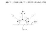
一方、エッチングにより基板上に形成される配線パターンの断面形状は、図8に示すように、上部よりも下部の幅が広い台形状になる。
このような断面形状の配線パターンに、図7に示すように拡散板101を介して照明光を照射すると、図8に示すように上方向からの光と斜め方向からの光が配線パターンに入射し、配線パターンの上面で反射した照明光が撮像素子121に入射するとともに、配線パターンの側面で反射した照明光の一部が撮像素子121に入射する。そのため、撮像手段120では、配線パターンの上面が明るく、配線パターンの側面がやや暗く撮像される。
ここで、撮像対象を照明する照明光が暗く、撮像素子121に入射する光の明るさが暗くなると、撮像素子121が取り込む画像は暗くなり、配線パターンの画像のコントラストが悪くなる。このため、配線パターンの上面と側面の区別がしにくくなる。
On the other hand, as shown in FIG. 8, the cross-sectional shape of the wiring pattern formed on the substrate by etching is a trapezoid with a lower width wider than the upper portion.
When the wiring pattern having such a cross-sectional shape is irradiated with illumination light through the diffusion plate 101 as shown in FIG. 7, light from the upper direction and light from the oblique direction enter the wiring pattern as shown in FIG. The illumination light reflected from the upper surface of the wiring pattern enters the image sensor 121 and a part of the illumination light reflected from the side surface of the wiring pattern enters the image sensor 121. Therefore, the imaging unit 120 captures an image with the upper surface of the wiring pattern being bright and the side surface of the wiring pattern being slightly dark.
Here, when the illumination light that illuminates the imaging target is dark and the brightness of the light incident on the image sensor 121 becomes dark, the image captured by the image sensor 121 becomes dark and the contrast of the image of the wiring pattern deteriorates. For this reason, it becomes difficult to distinguish the upper surface and the side surface of the wiring pattern.
また、配線パターンによっては、図8の点線に示すように、配線上部のエッジ部分が欠けて、線幅が狭くなっているものもある。このような配線パターンの「欠け」を配線パターンの欠陥として検出できるようにすることが望ましいが、撮像された配線パターンの画像のコントラストが悪く、配線パターンの上面と側面の区別がしにくくなると、配線パターン上面の形状が不明確になり、上記「欠け」を明瞭に撮像することができなくなる。
同軸照明により照明し撮像する撮像照明手段において、上記のような配線パターンの上部と側面部分とのコントラストを向上させ、上記エッジ部分の「欠け」を明瞭に撮像できるようにするためには、撮像対象を照明する照明光を明るくすることが必要であるが、それに加えて、上方向からの照明光の成分と斜め方向からの照射光の成分のバランスを適切にすることが望ましいと考えられる。
図7に示した撮像照明手段では、上方向からの光の成分の方に対して斜め方向からの光の成分が弱く、上記「欠け」を明瞭に撮像するのが難しかった。
すなわち、配線パターンの上面の形状、側面の形状をコントラスよく撮像するためには、撮像対象を照明する照明光を明るくするとともに、上方向からの光の成分に対して、斜め方向からの光の成分を増加させることが望ましい。
本発明は、上記問題点を解決するためになされたものであって、同軸照明を使った撮像照明手段において、ハーフミラー(ペリクル)の透過率を変えることなく、撮像対象の照度を明るくして、従来よりも明るい画像が撮像素子に取り込まれるようにするとともに、配線パターンのエッジ部分の欠け等により線幅の細くなっている部分をコントラストよく撮像することができるようにすることを目的とする。
Further, depending on the wiring pattern, as shown by the dotted line in FIG. 8, the edge portion at the upper part of the wiring is cut and the line width is narrowed. It is desirable to be able to detect such “chips” of the wiring pattern as defects in the wiring pattern, but when the contrast of the image of the captured wiring pattern is poor and it becomes difficult to distinguish the upper surface and the side surface of the wiring pattern, The shape of the upper surface of the wiring pattern becomes unclear, and it becomes impossible to clearly image the “chip”.
In the imaging illumination means for illuminating and imaging with coaxial illumination, in order to improve the contrast between the upper part and the side part of the wiring pattern as described above and to be able to clearly capture the “chip” of the edge part, imaging is performed. Although it is necessary to brighten the illumination light that illuminates the object, in addition to this, it is considered desirable to appropriately balance the illumination light component from the upper direction and the irradiation light component from the oblique direction.
In the imaging illumination unit shown in FIG. 7, the light component from the oblique direction is weaker than the light component from the upper direction, and it is difficult to clearly capture the “chip”.
That is, in order to image the shape of the upper surface and the side surface of the wiring pattern with a good contrast, the illumination light that illuminates the object to be imaged is brightened, and the light component from the oblique direction is compared with the light component from the upward direction. It is desirable to increase the ingredients.
The present invention has been made to solve the above-described problems, and in an imaging illumination unit using coaxial illumination, the illuminance of an imaging target is increased without changing the transmittance of a half mirror (pellicle). An object of the present invention is to allow a brighter image than the conventional one to be captured by an image sensor and to capture a portion with a narrow line width due to a lack of an edge portion of a wiring pattern with good contrast. .
本発明においては、以下のようにして前記課題を解決する。
(1)光源から出射した照明光がハーフミラーにより反射されて被照明物を照明し、該被照明物から反射する照明光が上記ハーフミラーを通過して撮像素子に入射し被照明物を撮像する撮像照明手段において、上記ハーフミラーの、撮像対象(撮像領域)の像が通過する部分を除いて、光源からの照明光が入射する側に、被照明物に向かって照明光を全反射する反射部材(ミラー)を取り付ける。
(2)上記ハーフミラーとしてペリクルを用いる。
(3)上記(1)(2)において、光源の光出射側に、光源の周辺部から出射した光を内側に屈折させる光学素子(例えばレンズ)を配置する。または、ハーフミラー(ペリクル)の周辺に設けた反射部材(ミラー)を、反射光が内側(被照射物側)に向かうように傾ける。
(4)上記(1)(2)において、光源を複数のLEDを平面状に並べたもので構成し、周辺部に並べたLEDを、出射する光の主光線が内側に向かうように傾けて配置する。
(5)基板上に形成されたパターンに照明光を照射して該パターンの画像を撮像する手段を備え、該撮像された画像に基づきパターンの良否を判定するパターン検査装置において、上記パターンに照明光を照射して撮像する手段として、上記(1)〜(4)の撮像照明手段を用いる。
In the present invention, the above-described problem is solved as follows.
(1) The illumination light emitted from the light source is reflected by the half mirror to illuminate the object to be illuminated, and the illumination light reflected from the object to be illuminated passes through the half mirror and enters the image sensor to capture the object to be illuminated. In the imaging illumination means, the illumination light is totally reflected toward the object to be illuminated on the side where the illumination light from the light source is incident, except for the portion of the half mirror through which the image of the imaging target (imaging area) passes. A reflection member (mirror) is attached.
(2) A pellicle is used as the half mirror.
(3) In the above (1) and (2), an optical element (for example, a lens) that refracts light emitted from the periphery of the light source inward is disposed on the light emission side of the light source. Alternatively, the reflecting member (mirror) provided around the half mirror (pellicle) is tilted so that the reflected light is directed inward (on the irradiated object side).
(4) In the above (1) and (2), the light source is composed of a plurality of LEDs arranged in a plane, and the LEDs arranged in the periphery are inclined so that the chief ray of the emitted light is directed inward. Deploy.
(5) In a pattern inspection apparatus that includes means for irradiating illumination light onto a pattern formed on a substrate to capture an image of the pattern, and determining the quality of the pattern based on the captured image, the pattern is illuminated The imaging illumination means of (1) to (4) above is used as means for imaging by irradiating light.
本発明においては、以下の効果を得ることができる。
(1)ハーフミラー(ペリクル)の周辺部に反射部材(ミラー)を設けたので、ハーフミラー(ペリクル)を通過していた光の一部が、撮像対象に向かって全反射され、撮像対象の照度を明るくすることができる。
(2)光源の周辺部から出射した光を内側に屈折させる光学素子(レンズ)を設けるか、または反射部材(ミラー)を反射光が内側に向かうように傾けて配置することにより、撮像領域に向かう照明光を増やすことができ、撮像領域をより明るく照明することができる。また、光源が複数のLEDである場合は、周辺部に並べたLEDを、出射する光の主光線が内側に向かうように傾けて配置することにより、撮像領域に向かう照明光を増やすことができ、撮像領域をより明るく照明することができる。
(3)撮像領域の照度を従来に比べて明るくすることができるので、撮像対象(基板)に形成されているパターンの反射率が低い場合であっても、基板とパターンのコントラストが低下するのを防ぐことができ、パターンを検出することができる。
また、撮像対象が配線パターンの場合、配線パターンに対して斜め方向から入射する光の成分を増加させることができるので、配線パターンの上面、側面の形状をコントラスよく撮像することができ、前記配線パターンの「欠け」ている部分等を明瞭に撮像することが可能となる。
したがって、上記構成の撮像照明手段を配線パターン検査装置に適用することにより、配線パターンが細くなっている部分等の欠陥を確実に検出することが可能となる。
In the present invention, the following effects can be obtained.
(1) Since the reflecting member (mirror) is provided in the periphery of the half mirror (pellicle), a part of the light that has passed through the half mirror (pellicle) is totally reflected toward the imaging target, Illuminance can be increased.
(2) An optical element (lens) that refracts the light emitted from the periphery of the light source to the inside is provided, or the reflection member (mirror) is disposed so that the reflected light is directed inward, so that the imaging region is The illuminating light to be directed can be increased, and the imaging region can be illuminated more brightly. In addition, when the light source is a plurality of LEDs, it is possible to increase the illumination light directed toward the imaging region by arranging the LEDs arranged in the periphery so that the chief rays of the emitted light are directed inward. The imaging area can be illuminated more brightly.
(3) Since the illuminance of the imaging region can be made brighter than before, even if the reflectance of the pattern formed on the imaging target (substrate) is low, the contrast between the substrate and the pattern is reduced. Can be prevented, and the pattern can be detected.
In addition, when the object to be imaged is a wiring pattern, it is possible to increase the component of light incident on the wiring pattern from an oblique direction, so that the shape of the upper and side surfaces of the wiring pattern can be imaged with good contrast. It is possible to clearly image a “missing” portion of the pattern.
Therefore, by applying the imaging illumination unit having the above configuration to the wiring pattern inspection apparatus, it is possible to reliably detect defects such as a portion where the wiring pattern is thin.
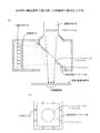
図1に、本発明の撮像照明手段の、第1の実施例の構成を示す。
図1(a)は、同軸照明の撮像照明手段の断面図であり、図1(b)は図1(a)において、ハーフミラー(ペリクル)を、照明光が入射する側から見た図である。
同図において、図7と同じ構成のものには同じ符号をつけており、前記背景技術として説明した部分と同じものについては詳細な説明は省略する。
図1において、撮像照明手段は、前記したように照明光を出射する光源100と、光源100からの照明光を被照明物に向かつて反射するハーフミラー110と、ハーフミラー110に対して被照明物とは反対側に配置された撮像手段120とを備える。撮像手段120は前記したように内部にCCDセンサなどの撮像素子121を備える。Sは、撮像素子121が撮像する領域(撮像領域)である。
照明光を出射する光源100は、前記したように平面状に複数配置されたLEDであり、光源100の光出射側には拡散板101が配置され、拡散板101により拡散された光は、斜めに配置されたハーフミラー(ペリクル)110に入射する。
FIG. 1 shows the configuration of the first embodiment of the imaging illumination means of the present invention.
FIG. 1A is a cross-sectional view of the imaging illumination means of coaxial illumination, and FIG. 1B is a view of the half mirror (pellicle) in FIG. 1A as viewed from the side on which the illumination light is incident. is there.
In this figure, the same components as those in FIG. 7 are denoted by the same reference numerals, and detailed description of the same components as those described as the background art will be omitted.
In FIG. 1, the imaging illuminating means includes the light source 100 that emits illumination light as described above, the half mirror 110 that reflects the illumination light from the light source 100 toward the object to be illuminated, and the half mirror 110 to be illuminated. And imaging means 120 disposed on the opposite side of the object. As described above, the imaging unit 120 includes the imaging element 121 such as a CCD sensor. S is an area (imaging area) where the image sensor 121 captures an image.
The light source 100 that emits the illumination light is a plurality of LEDs arranged in a plane as described above, and the diffusion plate 101 is disposed on the light emission side of the light source 100, and the light diffused by the diffusion plate 101 is oblique. Is incident on a half mirror (pellicle) 110 arranged on the surface.
本実施例において、図7と構成が異なる部分は、ハーフミラー(ペリクル)110の、撮像素子121の視野に当たる部分(撮像対象の撮像領域Sの像が通過する部分)以外であって、光源100からの照明光が入射する側に、照明光を撮像対象(基板)Wに向かって全反射する反射部材(ミラー)130を設けている点である。反射部材(ミラー)130は例えばアルミ板である。
従来、ハーフミラー(ペリクル)110に入射する照明光は、ハーフミラーの透過率と反射率が50:50であれば、半分しか反射されない。しかし、本実施例においては、反射部材(ミラー)130に入射する照明光は全反射され、基板Wを照明する。反射部材(ミラー)130に入射する光は散乱光であるので、反射した光の一部は撮像領域Sを照明する。
したがって、従来よりも撮像領域Sの照度を上げる(すなわち明るくする)ことができる。また、ハーフミラー(ペリクル)110の撮像対象の撮像領域Sの像が通過する部分の周囲に、反射部材130を設けているので、パターンに対して斜め方向から入射する光の成分を増加させることができる。このため、配線パターンの上面、側面をコントラスよく撮像することができ、「欠け」等の欠陥を明瞭に撮像することが可能となる。
In the present embodiment, a portion having a configuration different from that in FIG. 7 is a portion other than a portion of the half mirror (pellicle) 110 that corresponds to the field of view of the imaging element 121 (a portion through which an image of the imaging region S to be imaged passes). The reflection member (mirror) 130 that totally reflects the illumination light toward the imaging target (substrate) W is provided on the side on which the illumination light from the side is incident. The reflecting member (mirror) 130 is, for example, an aluminum plate.
Conventionally, illumination light incident on the half mirror (pellicle) 110 is only half reflected if the transmittance and reflectance of the half mirror are 50:50. However, in this embodiment, the illumination light incident on the reflecting member (mirror) 130 is totally reflected and illuminates the substrate W. Since the light incident on the reflecting member (mirror) 130 is scattered light, a part of the reflected light illuminates the imaging region S.
Therefore, the illuminance of the imaging region S can be increased (that is, brightened) compared to the conventional art. Further, since the reflecting member 130 is provided around the portion of the half mirror (pellicle) 110 through which the image of the imaging region S to be imaged passes, the light component incident from an oblique direction with respect to the pattern is increased. Can do. For this reason, the upper surface and the side surface of the wiring pattern can be imaged with high contrast, and defects such as “chips” can be clearly imaged.
また、ハーフミラー(ペリクル)110の、撮像素子の視野に当たる部分(撮像対象の撮像領域の像が通過する部分)には、反射部材(ミラー)130を設けないので、撮像素子121は、従来と同様にハーフミラー(ペリクル)110を介して、撮像領域Sの画像を受像することができる。
図1(b)は、反射部材(ミラー)130を設けたハーフミラー(ペリクル)110を、照明光が入射する側から見た図である。
従来と同様に、ハーフミラーであるペリクル110は、周辺部をフレーム111によって挟まれて支持されるが、その撮像素子121の視野に当たる部分(撮像対象の撮像領域Sの像が通過する部分、同図においては中央の円形の部分)を除く部分であって、光源からの照明光が入射する側に、反射部材(ミラー)130であるアルミ板を取り付けている。
In addition, since the reflecting member (mirror) 130 is not provided in the portion of the half mirror (pellicle) 110 that corresponds to the field of view of the imaging device (the portion through which the image of the imaging region to be imaged passes), the imaging device 121 is different from the conventional one. Similarly, the image of the imaging region S can be received via the half mirror (pellicle) 110.
FIG. 1B is a view of a half mirror (pellicle) 110 provided with a reflecting member (mirror) 130 as viewed from the side on which illumination light is incident.
As in the prior art, the pellicle 110, which is a half mirror, is supported with its peripheral part sandwiched between frames 111, but the part that corresponds to the field of view of the image sensor 121 (the part through which the image of the imaging region S to be imaged passes, In the figure, an aluminum plate which is a reflecting member (mirror) 130 is attached to a portion excluding the central circular portion) on the side where the illumination light from the light source is incident.
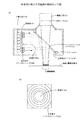
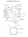
図2は、上記第1の実施例の変形例である。
上記実施例においては、ペリクル110を支持するフレーム111とは別に反射部材(ミラー)130を設けた。しかし、図2においては、ペリクル110の大きさを、撮像素子の視野に当たる大きさ(撮像対象の撮像領域の像が通過する大きさ)にまで小さくし、その分フレーム131を大きくしている。また、フレーム131の、光源からの照明光が入射する面を反射面に加工している。
このように、ペリクル110を支持するフレーム111に反射面加工を施し、ペリクル110の支持と照明光の反射を兼用するようにしても良い。
FIG. 2 is a modification of the first embodiment.
In the above embodiment, the reflecting member (mirror) 130 is provided separately from the frame 111 that supports the pellicle 110. However, in FIG. 2, the size of the pellicle 110 is reduced to a size corresponding to the field of view of the imaging element (a size through which an image of the imaging region to be imaged passes), and the frame 131 is increased accordingly. Further, the surface of the frame 131 on which the illumination light from the light source is incident is processed into a reflective surface.
In this way, the frame 111 that supports the pellicle 110 may be processed to have a reflecting surface so that both the support of the pellicle 110 and the reflection of illumination light are combined.
次に、図3、図4、図5を用いて、第2、第3、第4の実施例を説明する。いずれの実施例も、第1の実施例において、斜め方向からの照明光を増加させて、撮像領域の照度をさらに上げる(明るくする)工夫である。即ち、光源100から出射する照明光は、拡散板101を介するとはいえ、直進する成分が大きい。そのため、光源100の周辺部から直進する光の成分を、内側即ち基板Wの撮像領域の方向に曲げるように構成する。
図3(a)は、第2の実施例の構成を示す図である。
本実施例においては、光源100とハーフミラー(ペリクル)110の間(同図においては拡散板101の光出射側)に、光源の周辺部から出射した光を内側に屈折させる光学素子102を設けている。同図においては、この光学素子102としてフレネルレンズを用いたが通常の凸レンズでも良い。
図3(b)は、本実施例の光学素子(フレネルレンズ)102を光出射側から見た図である。フレネルレンズは、凸レンズを同心円状の領域に分割し厚みを減らしたレンズであり、のこぎり状の断面を持つ。
Next, the second, third, and fourth embodiments will be described with reference to FIGS. 3, 4, and 5. FIG. In any of the embodiments, the illumination light from the oblique direction is increased in the first embodiment to further increase (brighten) the illuminance of the imaging region. That is, the illumination light emitted from the light source 100 has a large component that travels straight though the diffusion plate 101. Therefore, the light component traveling straight from the periphery of the light source 100 is configured to bend inward, that is, toward the imaging region of the substrate W.
FIG. 3A is a diagram showing the configuration of the second embodiment.
In this embodiment, an optical element 102 is provided between the light source 100 and the half mirror (pellicle) 110 (in the figure, the light exit side of the diffuser plate 101) to refract the light emitted from the periphery of the light source inward. ing. In this figure, a Fresnel lens is used as the optical element 102, but a normal convex lens may be used.
FIG. 3B is a view of the optical element (Fresnel lens) 102 of this embodiment as viewed from the light emission side. A Fresnel lens is a lens in which a convex lens is divided into concentric circular regions to reduce the thickness, and has a saw-like cross section.
このフレネルレンズ102により、光源100の周辺部から出射する光のうち直進する成分の光を、内側に曲げる(屈折させる)ことができる。内側に屈折した光は、ハーフミラー(ペリクル)110の周辺部に設けた反射部材(ミラー)130により、撮像対象の撮像領域Sの方向に反射する。
これにより、光源100から直進する明るい成分の光を、撮像領域Sに照射することができ、撮像領域Sの照度を上げる(明るくする)ことができる。また、パターンに対して斜め方向から入射する光の成分を増加させることができる。
なお、光源の中央部の光は内側に曲げなくても、撮像領域Sを照射するので、フレネルレンズ102の中央部はレンズがなく貫通孔102aになっている。
The Fresnel lens 102 can bend (refracted) inwardly the light component that travels straight out of the light emitted from the periphery of the light source 100. The light refracted inward is reflected in the direction of the imaging region S to be imaged by a reflecting member (mirror) 130 provided in the periphery of the half mirror (pellicle) 110.
Thereby, the light component 100 that travels straight from the light source 100 can be irradiated onto the imaging region S, and the illuminance of the imaging region S can be increased (brightened). Further, it is possible to increase the component of light incident from the oblique direction with respect to the pattern.
Since the light at the center of the light source irradiates the imaging region S without being bent inward, the center of the Fresnel lens 102 has no lens and is a through hole 102a.
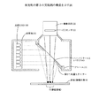
図4は、第3の実施例の構成を示す図である。
本実施例においては、ハーフミラー(ペリクル)110の周辺部に設けた反射部材(ミラー)130を、光源100からの照明光が内側に向かって反射するように傾けて配置している。
これにより、光源100から直進する明るい成分の光を、撮像領域Sに照射することができ、撮像領域Sの照度を上げる(明るくする)ことができる。また、パターンに対して斜め方向から入射する光の成分を増加させることができる。
FIG. 4 is a diagram showing the configuration of the third embodiment.
In this embodiment, the reflecting member (mirror) 130 provided in the peripheral part of the half mirror (pellicle) 110 is disposed so as to be inclined so that the illumination light from the light source 100 is reflected inward.
Thereby, the light component 100 that travels straight from the light source 100 can be irradiated onto the imaging region S, and the illuminance of the imaging region S can be increased (brightened). Further, it is possible to increase the component of light incident from the oblique direction with respect to the pattern.
図5は、第4の実施例の構成を示す図である。
光源100が、複数のLEDを平面状に並べたものである場合は、周辺部に配置したLEDを、出射する光の主光線が内側に向くように傾けて配置する。
これにより、各LEDから直進して出射する明るい成分の光を、撮像領域Sに照射することができ、撮像領域Sの照度を上げる(明るくする)ことができる。また、パターンに対して斜め方向から入射する光の成分を増加させることができる。
なお、第2の実施例において示したフレネルレンズの使用、第3の実施例において示した反射部材(ミラー)を傾けて配置すること、第4の実施例において示したLEDを傾斜して配置させることは、それぞれを互いに組み合わせて用いてもよい。これらを組み合わせることにより、照明の効率を上げることができる。
FIG. 5 is a diagram showing the configuration of the fourth embodiment.
When the light source 100 has a plurality of LEDs arranged in a plane, the LEDs arranged in the peripheral portion are arranged so as to be inclined so that the chief ray of the emitted light faces inward.
Thereby, the light of the bright component which goes straight out from each LED can be irradiated to the imaging region S, and the illuminance of the imaging region S can be increased (brightened). Further, it is possible to increase the component of light incident from the oblique direction with respect to the pattern.
It should be noted that the Fresnel lens shown in the second embodiment is used, the reflecting member (mirror) shown in the third embodiment is inclined, and the LEDs shown in the fourth embodiment are inclined. It may be used in combination with each other. By combining these, the illumination efficiency can be increased.
なお、以上の説明では、ハーフミラー(ペリクル)110の透過率が50%(反射率も50%)の場合について説明したが、ハーフミラーの透過率を50%以上とすることで、撮像素子121に入射する画像をより明るくすることができる。
すなわち、ハーフミラー(ペリクル)110の透過率を50%以上とすると、光源100からハーフミラー(ペリクル)110に入射して撮像対象側に反射する光の量は減少するものの、反射部材130で反射して撮像対象側に入射する光の量は変わらないので、撮像素子に入射する照明光は、それほど減少しない。
一方、ハーフミラーの透過率を大きくすることで、撮像対象で反射してハーフミラー(ペリクル)110を介して撮像素子121に入射する光の量は多くなるので、結果として撮像素子121に入射する光の量は多くなり、撮像される画像をより明るくすることができる。
In the above description, the case where the transmittance of the half mirror (pellicle) 110 is 50% (the reflectance is also 50%) has been described, but the imaging element 121 can be obtained by setting the transmittance of the half mirror to 50% or more. It is possible to make the image incident on the screen brighter.
That is, when the transmittance of the half mirror (pellicle) 110 is 50% or more, the amount of light that enters the half mirror (pellicle) 110 from the light source 100 and reflects to the imaging target side decreases, but is reflected by the reflecting member 130. Since the amount of light incident on the imaging target side does not change, the illumination light incident on the imaging element does not decrease so much.
On the other hand, by increasing the transmittance of the half mirror, the amount of light that is reflected by the imaging target and is incident on the imaging element 121 via the half mirror (pellicle) 110 increases. As a result, the incident light is incident on the imaging element 121. The amount of light increases and the captured image can be brighter.
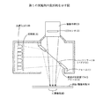
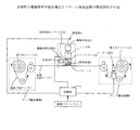
図6は、本発明の撮像照明手段を備えたパターン検査装置の構成例を示す図である。
同図において、1はポリイミド(樹脂)等からなるTABテープ等の光透過性の基板、2は基板1上に形成され銅等の金属からなる配線パターン等のパターン、3は検査部であり、上記で説明した本発明の撮像照明手段が使用されている。
4は制御部、5はテープ搬送機構、51は送り出しリール、52は巻き取りリール、53はマーカー部、6は検査領域である。ここで、検査領域6とは照明光が照射され、撮像手段120により撮像される撮像領域である。
基板(TABテープ)1は、送り出しリール51から送りだされて検査領域6でパターン2の良否が判定され、マーカー部53を経て、巻き取りリール52に巻き取られる。
マーカー部53では、不良と判定されたパターン2に対しその部分が不良品であることを目視ですぐ確認できるようにパンチでの穿孔や、色塗り等のマークを施す。
制御部4は、予めパターン検査の基準となる基準パターンが入力されており、撮像したパターン2と基準パターンとを比較し製品の良否を判定する。また、制御部4は、検査部3、マーカー部53、及びテープ搬送機構5の動作を制御する。
検査部1においては、撮像照明手段31により基板(TABテープ)1に対して同軸照明が行われ撮像される。
FIG. 6 is a diagram illustrating a configuration example of a pattern inspection apparatus including the imaging illumination unit of the present invention.
In the figure, 1 is a light-transmitting substrate such as a TAB tape made of polyimide (resin) or the like, 2 is a pattern such as a wiring pattern formed on the substrate 1 and made of metal such as copper, 3 is an inspection portion, The imaging illumination means of the present invention described above is used.
4 is a control unit, 5 is a tape transport mechanism, 51 is a delivery reel, 52 is a take-up reel, 53 is a marker unit, and 6 is an inspection area. Here, the inspection area 6 is an imaging area that is irradiated with illumination light and imaged by the imaging means 120.
The substrate (TAB tape) 1 is sent out from the delivery reel 51, and the quality of the pattern 2 is judged in the inspection area 6, and taken up on the take-up reel 52 through the marker portion 53.
In the marker portion 53, a mark such as punching or coloring is applied to the pattern 2 determined to be defective so that the portion can be immediately confirmed visually as a defective product.
The
In the inspection unit 1, coaxial illumination is performed on the substrate (TAB tape) 1 by the imaging illumination unit 31 and an image is captured.
撮像照明手段31において、照明光は、平面状に並べられた複数個のLEDからなる光源100から出射し、反射部材(ミラー)130とハーフミラー(ペリクル)110により反射され、基板1上の検査領域6に対して直交またはほぼ直交するように照射される。 そして、パターン2により反射された光はハーフミラー(ペリクル)110を通過して撮像手段120に入射する。
撮像手段120は、照明光の波長に受光感度を有する、例えば、CCDラインセンサまたはエリアセンサが用いられる。また、本実施例においては、撮像手段120の光入射側には、TABテープからなる基板1のパターン2の検査を行う領域を拡大して投影するレンズ32が設けられており、レンズ32は複数のレンズが組み合わされて鏡筒に収納されている。
In the imaging illumination unit 31, the illumination light is emitted from the light source 100 composed of a plurality of LEDs arranged in a plane, reflected by the reflecting member (mirror) 130 and the half mirror (pellicle) 110, and inspected on the substrate 1. Irradiation is performed so as to be orthogonal or substantially orthogonal to the region 6. Then, the light reflected by the pattern 2 passes through the half mirror (pellicle) 110 and enters the imaging unit 120.
As the imaging unit 120, for example, a CCD line sensor or an area sensor having light receiving sensitivity at the wavelength of illumination light is used. In the present embodiment, a lens 32 for projecting an enlarged region to be inspected for the pattern 2 of the substrate 1 made of TAB tape is provided on the light incident side of the image pickup unit 120. These lenses are combined and stored in a lens barrel.
照明光が基板1に対して直交またはほぼ直交するように照射されると、基板1に形成されているパターン2の表面がほぼ平らな状態であれば、パターンは銅等の金属であるので照明光は反射され、撮像手段120に入射する。パターン2以外の部分に照射された照明光は、基板1は樹脂であるので、基板1を透過または基板1に吸収され、撮像手段120に入射しない。
これにより、撮像手段120により撮像された画像は、基板1のパターンがある部分とない部分及びパターンの上面と側面とでコントラストに差ができ、制御部4にて画像処理を行うことにより、パターンのエッジを検出してパターンの幅を求めることができる。
制御部4は、このようにして求めたパターンの幅を、あらかじめ記憶しておいた基準パターンの幅と比較し製品の良否を判定する。
When the illumination light is irradiated so as to be orthogonal or almost orthogonal to the substrate 1, if the surface of the pattern 2 formed on the substrate 1 is in a substantially flat state, the pattern is a metal such as copper. The light is reflected and enters the imaging means 120. Illumination light irradiated to portions other than the pattern 2 is transmitted through the substrate 1 or absorbed by the substrate 1 and does not enter the imaging means 120 because the substrate 1 is made of resin.
As a result, the image captured by the image capturing means 120 can have a difference in contrast between the portion with and without the pattern of the substrate 1 and the upper and side surfaces of the pattern. The width of the pattern can be obtained by detecting the edge.
The
本実施例のパターン検査装置においては、上記実施例に示した撮像照明手段を使用しているので、撮像領域の照度を従来に比べて明るくすることができる。したがって、撮像対象(基板)に形成されているパターンの反射率が低い場合であっても、基板とパターンのコントラストが低下するのを防ぐことができ、パターンを検出することができる。
また、配線パターンに対して上方向からの光の成分と斜め方向からの光の成分をバランスよく照射できるので、パターンの上面の形状、側面の形状をコントラスよく撮像することができ、パターンの欠陥を確実に検出することができる。
In the pattern inspection apparatus of the present embodiment, since the imaging illumination unit shown in the above embodiment is used, the illuminance of the imaging area can be made brighter than before. Therefore, even when the reflectance of the pattern formed on the imaging target (substrate) is low, it is possible to prevent the contrast between the substrate and the pattern from being lowered and to detect the pattern.
In addition, since the light component from above and the light component from oblique direction can be irradiated with good balance to the wiring pattern, the shape of the upper surface and side surface of the pattern can be imaged with good contrast, and the pattern defect Can be reliably detected.
1 基板(TABテープ)
2 パターン
3 検査部
31 撮像照明手段
32 レンズ
4 制御部
5 テープ搬送機構
51 送り出しリール
52 巻き取りリール
53 マーカー部
6 検査領域
100 光源
101 拡散板
102 フレネルレンズ
110 ハーフミラー
111 フレーム
120 撮像手段
121 撮像素子
130 反射部材
131 表面が反射面であるフレーム
W 基板
S 撮像領域
1 Substrate (TAB tape)
2 pattern 3 inspection unit 31 imaging illumination unit 32
Claims (6)
上記ハーフミラーの、被照明物から反射して撮像素子に入射する照明光が通過する部分の外側であって、光源からの照明光が入射する側に、
該照明光を被照明物に向かって反射する反射部材を設ける
ことを特徴とする撮像照明手段。 Imaging illumination in which illumination light emitted from a light source is reflected by a half mirror to illuminate an object to be illuminated, and illumination light reflected from the illumination object passes through the half mirror and enters the imaging device to image the illumination object In the means
On the outer side of the portion of the half mirror where the illumination light reflected from the object to be illuminated and incident on the image sensor passes, on the side where the illumination light from the light source is incident,
An imaging illumination means, comprising: a reflection member that reflects the illumination light toward an object to be illuminated.
ことを特徴とする請求項1に記載の撮像照明手段。 2. The imaging illumination means according to claim 1, wherein the half mirror is a pellicle.
ことを特徴とする請求項1または請求項2に記載の撮像照明手段。 The imaging illumination unit according to claim 1 or 2, wherein an optical element that refracts light emitted from a peripheral portion of the light source inward is disposed between the light source and the half mirror.
ことを特徴とする請求項1または請求項2に記載の撮像照明手段。 The imaging illumination unit according to claim 1 or 2, wherein the reflection member is arranged so as to be inclined so that the illumination light is reflected inward.
ことを特徴とする請求項1または請求項2に記載の撮像照明手段。 The light source includes a plurality of LEDs arranged in a plane, and the peripheral LEDs of the plurality of LEDs are arranged so as to be inclined so that the principal ray of the emitted light is directed inward. The imaging illumination means according to claim 1 or 2.
上記パターンに照明光を照射して撮像する手段は、請求項1,2,3,4または請求項5に記載の撮像照明手段である
ことを特徴とするパターン検査装置。 In a pattern inspection apparatus comprising a means for irradiating illumination light to a pattern formed on a substrate and capturing an image of the pattern, and determining whether the pattern is good or not based on the captured image,
The pattern inspection apparatus according to claim 1, wherein the means for irradiating the pattern with illumination light to pick up an image is the image pickup illumination means according to claim 1.
Priority Applications (1)
| Application Number | Priority Date | Filing Date | Title |
|---|---|---|---|
| JP2009260885A JP2011106912A (en) | 2009-11-16 | 2009-11-16 | Imaging illumination means and pattern inspection device |
Applications Claiming Priority (1)
| Application Number | Priority Date | Filing Date | Title |
|---|---|---|---|
| JP2009260885A JP2011106912A (en) | 2009-11-16 | 2009-11-16 | Imaging illumination means and pattern inspection device |
Publications (1)
| Publication Number | Publication Date |
|---|---|
| JP2011106912A true JP2011106912A (en) | 2011-06-02 |
Family
ID=44230562
Family Applications (1)
| Application Number | Title | Priority Date | Filing Date |
|---|---|---|---|
| JP2009260885A Pending JP2011106912A (en) | 2009-11-16 | 2009-11-16 | Imaging illumination means and pattern inspection device |
Country Status (1)
| Country | Link |
|---|---|
| JP (1) | JP2011106912A (en) |
Cited By (5)
| Publication number | Priority date | Publication date | Assignee | Title |
|---|---|---|---|---|
| JP5027946B1 (en) * | 2011-12-28 | 2012-09-19 | 新明和工業株式会社 | Inspection system |
| KR101728599B1 (en) | 2015-03-16 | 2017-04-20 | 유광룡 | Lighting device and testing device including the same |
| US10379057B2 (en) | 2014-10-31 | 2019-08-13 | Kla-Tencor Corporation | Illumination system, inspection tool with illumination system, and method of operating an illumination system |
| WO2022267863A1 (en) * | 2021-06-22 | 2022-12-29 | 威海华菱光电股份有限公司 | Contact-type image sensor |
| KR20230026826A (en) * | 2021-08-18 | 2023-02-27 | (주)다우시스템 | Illumination device for line scan inspection |
-
2009
- 2009-11-16 JP JP2009260885A patent/JP2011106912A/en active Pending
Cited By (6)
| Publication number | Priority date | Publication date | Assignee | Title |
|---|---|---|---|---|
| JP5027946B1 (en) * | 2011-12-28 | 2012-09-19 | 新明和工業株式会社 | Inspection system |
| US10379057B2 (en) | 2014-10-31 | 2019-08-13 | Kla-Tencor Corporation | Illumination system, inspection tool with illumination system, and method of operating an illumination system |
| KR101728599B1 (en) | 2015-03-16 | 2017-04-20 | 유광룡 | Lighting device and testing device including the same |
| WO2022267863A1 (en) * | 2021-06-22 | 2022-12-29 | 威海华菱光电股份有限公司 | Contact-type image sensor |
| KR20230026826A (en) * | 2021-08-18 | 2023-02-27 | (주)다우시스템 | Illumination device for line scan inspection |
| KR102748327B1 (en) | 2021-08-18 | 2024-12-31 | (주)다우시스템 | Illumination device for line scan inspection |
Similar Documents
| Publication | Publication Date | Title |
|---|---|---|
| TWI442016B (en) | A light source for illumination and a pattern inspection device using it | |
| JP6042402B2 (en) | Illumination module and visual inspection system using the same | |
| US7957636B2 (en) | Illumination apparatus and appearance inspection apparatus including the same | |
| US8363214B2 (en) | Surface inspection apparatus | |
| JP2010151479A (en) | Wiring pattern inspecting device | |
| KR101120226B1 (en) | Surface inspecting apparatus | |
| TW200842347A (en) | Pattern checking device and pattern checking mehtod | |
| CN104279456A (en) | Illumination system for optical detection, detection system using illumination system and detection method | |
| KR102540780B1 (en) | Die bonding apparatus and manufacturing method of semiconductor device | |
| US20050247895A1 (en) | Surface inspecting apparatus and surface inspecting method | |
| JP2011106912A (en) | Imaging illumination means and pattern inspection device | |
| JP2012002648A (en) | Wafer detect inspection device | |
| KR101208573B1 (en) | Optical condensing member and illumination unit, and optical inspection apparatus using the same | |
| JP2004347417A (en) | Pattern inspection equipment | |
| KR20050018822A (en) | Automated optical inspection machine | |
| JP2012042254A (en) | Lens defect inspection method | |
| JP6616040B1 (en) | Appearance inspection device | |
| JP2004212353A (en) | Optical inspection apparatus | |
| JP2015102364A (en) | Appearance inspection device | |
| JP2010190740A (en) | Substrate inspection device, method, and program | |
| JP7560149B2 (en) | Illumination device and imaging system | |
| JP6455029B2 (en) | Inspection method and inspection apparatus | |
| TW201520542A (en) | Illumination device for high-speed wide mirror wafer surface detection | |
| JP2010203892A (en) | Substrate inspecting method | |
| JP2008275410A (en) | Optical inspection device and method of printed circuit board |