JP6899314B2 - Adsorption method - Google Patents
Adsorption method Download PDFInfo
- Publication number
- JP6899314B2 JP6899314B2 JP2017221853A JP2017221853A JP6899314B2 JP 6899314 B2 JP6899314 B2 JP 6899314B2 JP 2017221853 A JP2017221853 A JP 2017221853A JP 2017221853 A JP2017221853 A JP 2017221853A JP 6899314 B2 JP6899314 B2 JP 6899314B2
- Authority
- JP
- Japan
- Prior art keywords
- contact
- adsorption
- fabry
- membrane structure
- collet
- Prior art date
- Legal status (The legal status is an assumption and is not a legal conclusion. Google has not performed a legal analysis and makes no representation as to the accuracy of the status listed.)
- Active
Links
Images


Classifications
-
- H—ELECTRICITY
- H01—ELECTRIC ELEMENTS
- H01L—SEMICONDUCTOR DEVICES NOT COVERED BY CLASS H10
- H01L21/00—Processes or apparatus adapted for the manufacture or treatment of semiconductor or solid state devices or of parts thereof
- H01L21/67—Apparatus specially adapted for handling semiconductor or electric solid state devices during manufacture or treatment thereof; Apparatus specially adapted for handling wafers during manufacture or treatment of semiconductor or electric solid state devices or components ; Apparatus not specifically provided for elsewhere
- H01L21/677—Apparatus specially adapted for handling semiconductor or electric solid state devices during manufacture or treatment thereof; Apparatus specially adapted for handling wafers during manufacture or treatment of semiconductor or electric solid state devices or components ; Apparatus not specifically provided for elsewhere for conveying, e.g. between different workstations
- H01L21/67703—Apparatus specially adapted for handling semiconductor or electric solid state devices during manufacture or treatment thereof; Apparatus specially adapted for handling wafers during manufacture or treatment of semiconductor or electric solid state devices or components ; Apparatus not specifically provided for elsewhere for conveying, e.g. between different workstations between different workstations
- H01L21/67721—Apparatus specially adapted for handling semiconductor or electric solid state devices during manufacture or treatment thereof; Apparatus specially adapted for handling wafers during manufacture or treatment of semiconductor or electric solid state devices or components ; Apparatus not specifically provided for elsewhere for conveying, e.g. between different workstations between different workstations the substrates to be conveyed not being semiconductor wafers or large planar substrates, e.g. chips, lead frames
-
- G—PHYSICS
- G02—OPTICS
- G02B—OPTICAL ELEMENTS, SYSTEMS OR APPARATUS
- G02B5/00—Optical elements other than lenses
- G02B5/20—Filters
- G02B5/28—Interference filters
- G02B5/284—Interference filters of etalon type comprising a resonant cavity other than a thin solid film, e.g. gas, air, solid plates
-
- B—PERFORMING OPERATIONS; TRANSPORTING
- B25—HAND TOOLS; PORTABLE POWER-DRIVEN TOOLS; MANIPULATORS
- B25J—MANIPULATORS; CHAMBERS PROVIDED WITH MANIPULATION DEVICES
- B25J15/00—Gripping heads and other end effectors
- B25J15/06—Gripping heads and other end effectors with vacuum or magnetic holding means
-
- H—ELECTRICITY
- H01—ELECTRIC ELEMENTS
- H01L—SEMICONDUCTOR DEVICES NOT COVERED BY CLASS H10
- H01L21/00—Processes or apparatus adapted for the manufacture or treatment of semiconductor or solid state devices or of parts thereof
- H01L21/67—Apparatus specially adapted for handling semiconductor or electric solid state devices during manufacture or treatment thereof; Apparatus specially adapted for handling wafers during manufacture or treatment of semiconductor or electric solid state devices or components ; Apparatus not specifically provided for elsewhere
- H01L21/68—Apparatus specially adapted for handling semiconductor or electric solid state devices during manufacture or treatment thereof; Apparatus specially adapted for handling wafers during manufacture or treatment of semiconductor or electric solid state devices or components ; Apparatus not specifically provided for elsewhere for positioning, orientation or alignment
-
- H—ELECTRICITY
- H01—ELECTRIC ELEMENTS
- H01L—SEMICONDUCTOR DEVICES NOT COVERED BY CLASS H10
- H01L21/00—Processes or apparatus adapted for the manufacture or treatment of semiconductor or solid state devices or of parts thereof
- H01L21/67—Apparatus specially adapted for handling semiconductor or electric solid state devices during manufacture or treatment thereof; Apparatus specially adapted for handling wafers during manufacture or treatment of semiconductor or electric solid state devices or components ; Apparatus not specifically provided for elsewhere
- H01L21/683—Apparatus specially adapted for handling semiconductor or electric solid state devices during manufacture or treatment thereof; Apparatus specially adapted for handling wafers during manufacture or treatment of semiconductor or electric solid state devices or components ; Apparatus not specifically provided for elsewhere for supporting or gripping
- H01L21/6838—Apparatus specially adapted for handling semiconductor or electric solid state devices during manufacture or treatment thereof; Apparatus specially adapted for handling wafers during manufacture or treatment of semiconductor or electric solid state devices or components ; Apparatus not specifically provided for elsewhere for supporting or gripping with gripping and holding devices using a vacuum; Bernoulli devices
Description
本発明は、吸着方法に関する。 The present invention relates to an adsorption method.
従来のファブリペロー干渉フィルタとして、基板と、基板上において空隙を介して互いに対向する固定ミラー及び可動ミラーと、空隙を画定する中間層と、を備えるものが知られている(例えば、特許文献1参照)。 As a conventional Fabry-Perot interference filter, a substrate, a fixed mirror and a movable mirror facing each other via a gap on the substrate, and an intermediate layer for defining the gap are known (for example, Patent Document 1). reference).
上述したようなファブリペロー干渉フィルタのチップを個別に搬送する際には、例えば吸着コレットを用いてチップを個別に吸着しながら移送することが考えられる。この場合には、吸着を解除したときに、ファブリペロー干渉フィルタの姿勢及び位置が変化することを抑制し、吸着コレットからファブリペロー干渉フィルタを安定して脱離させることが望ましい。 When the chips of the Fabry-Perot interference filter as described above are individually transported, it is conceivable to transfer the chips while individually adsorbing them using, for example, a suction collet. In this case, it is desirable to suppress the change in the posture and position of the Fabry-Perot interference filter when the adsorption is released, and to stably detach the Fabry-Perot interference filter from the adsorption collet.
本発明は、ファブリペロー干渉フィルタを安定して脱離させることが可能な吸着方法を提供することを目的とする。 An object of the present invention is to provide an adsorption method capable of stably desorbing a Fabry-Perot interference filter.
本発明に係る吸着コレットは、基板と、基板上に設けられ、基板と反対側に臨む主面を含む積層構造部と、を備えるファブリペロー干渉フィルタを吸着コレットを用いて吸着する吸着方法であって、主面に対向するように吸着コレットを配置する第1工程と、第1工程の後に、吸着コレットをファブリペロー干渉フィルタに接触させる第2工程と、第2工程の後に、吸着コレットによってファブリペロー干渉フィルタを吸着する第3工程と、を備え、吸着コレットは、表面を有する本体部と、表面から突出するように表面に設けられ、吸気のための開口が形成された一対の第1接触面を含む接触部と、を備え、積層構造部には、空隙を介して互いに対向し且つ互いの距離が可変とされた第1ミラー部及び第2ミラー部と主面の一部とを含むメンブレン構造部と、主面に交差する方向からみてメンブレン構造部を挟んで互いに対向するように配置された一対の第1電極端子と、が設けられており、第1工程においては、表面が主面に対向すると共に、第1接触面のそれぞれが第1電極端子のそれぞれに対向するように吸着コレットを配置し、第2工程においては、第1接触面のそれぞれを第1電極端子のそれぞれに接触させ、第3工程においては、第1接触面の開口を介した吸気により第1電極端子のそれぞれを第1接触面に吸着する。 The adsorption collet according to the present invention is an adsorption method for adsorbing a Fabric Perot interference filter including a substrate and a laminated structure portion provided on the substrate and including a main surface facing the opposite side of the substrate using the adsorption collet. The first step of arranging the suction collet so as to face the main surface, the second step of bringing the suction collet into contact with the fabric perot interference filter after the first step, and the second step of contacting the suction collet with the fabric perot interference filter, and after the second step, the suction collet is used for fabrication. A third step of adsorbing the Perot interference filter is provided, and the adsorption collet is provided on the main body having a surface and a pair of first contacts which are provided on the surface so as to protrude from the surface and have an opening for intake. A contact portion including a surface, and a laminated structure portion includes a first mirror portion and a second mirror portion and a part of the main surface which face each other through a gap and have a variable distance from each other. A membrane structure portion and a pair of first electrode terminals arranged so as to face each other across the membrane structure portion when viewed from the direction intersecting the main surface are provided, and in the first step, the surface is mainly provided. The adsorption collets are arranged so as to face the surfaces and each of the first contact surfaces faces each of the first electrode terminals. In the second step, each of the first contact surfaces is attached to each of the first electrode terminals. In the third step, each of the first electrode terminals is attracted to the first contact surface by the intake air through the opening of the first contact surface.
この吸着方法の吸着対象となるファブリペロー干渉フィルタは、基板と基板上に設けられた積層構造部とを備えている。積層構造部には、空隙を介して互いに対向し且つ互いの距離が可変とされた第1ミラー部及び第2ミラー部を有するメンブレン構造部と、メンブレン構造部を挟んで互いに対向するように配置された一対の第1電極端子と、が設けられている。これに対して、この吸着方法に用いる吸着コレットにおいては、本体部の表面に突設された接触部が、吸気のための開口が形成された第1接触面を含む。そして、第1工程においては、ファブリペロー干渉フィルタの主面に吸着コレットの表面が対向するように吸着コレットを配置する。このとき、第1接触面のそれぞれが第1電極端子のそれぞれに対向するようにする。続いて、第2工程においては、吸着コレットをファブリペロー干渉フィルタに接触させる。このとき、第1接触面のそれぞれを第1電極端子のそれぞれに接触させる。そして、第3工程においては、吸着コレットによってファブリペロー干渉フィルタを吸着する。このとき、第1接触面の開口を介した吸気により第1電極端子のそれぞれを第1接触面に吸着する。これにより、ファブリペロー干渉フィルタの吸着に際して、第1電極端子といった限定的な範囲を吸着することが可能となる。よって、適度な吸着が得られる結果、吸着を解除した際にファブリペロー干渉フィルタを安定して脱離させることが可能となる。 The Fabry-Perot interference filter to be adsorbed by this adsorption method includes a substrate and a laminated structure portion provided on the substrate. In the laminated structure portion, a membrane structure portion having a first mirror portion and a second mirror portion having a first mirror portion and a second mirror portion whose distances are variable from each other and facing each other through a gap is arranged so as to face each other with the membrane structure portion interposed therebetween. A pair of first electrode terminals and the like are provided. On the other hand, in the suction collet used in this suction method, the contact portion projecting from the surface of the main body portion includes the first contact surface having an opening for intake air. Then, in the first step, the adsorption collet is arranged so that the surface of the adsorption collet faces the main surface of the Fabry-Perot interference filter. At this time, each of the first contact surfaces is made to face each of the first electrode terminals. Subsequently, in the second step, the adsorption collet is brought into contact with the Fabry-Perot interference filter. At this time, each of the first contact surfaces is brought into contact with each of the first electrode terminals. Then, in the third step, the Fabry-Perot interference filter is adsorbed by the adsorption collet. At this time, each of the first electrode terminals is attracted to the first contact surface by the intake air through the opening of the first contact surface. This makes it possible to adsorb a limited range such as the first electrode terminal when adsorbing the Fabry-Perot interference filter. Therefore, as a result of obtaining an appropriate adsorption, the Fabry-Perot interference filter can be stably desorbed when the adsorption is released.
本発明に係る吸着方法においては、第1電極端子は、主面から突出した頂面を含み、前記第2工程においては、第1接触面を前記頂面に接触させてもよい。この場合、第2工程において、接触部の第1接触面を、メンブレン構造部よりも突出した第1電極端子に接触させることになる。したがって、吸着コレットがメンブレン構造部に接触しないか、接触したとしてもメンブレン構造部への負荷が低減される。よって、ファブリペロー干渉フィルタの吸着に際して、メンブレン構造部の破損が避けられ、ファブリペロー干渉フィルタの不良品の発生が抑制される。 In the adsorption method according to the present invention, the first electrode terminal includes a top surface protruding from the main surface, and in the second step, the first contact surface may be brought into contact with the top surface. In this case, in the second step, the first contact surface of the contact portion is brought into contact with the first electrode terminal protruding from the membrane structure portion. Therefore, the adsorption collet does not come into contact with the membrane structure, or even if it comes into contact, the load on the membrane structure is reduced. Therefore, when the Fabry-Perot interference filter is adsorbed, the membrane structure is prevented from being damaged, and the occurrence of defective Fabry-Perot interference filters is suppressed.
本発明に係る吸着方法においては、第1接触面が第1電極端子に接触した状態において第1接触面におけるメンブレン構造部側に位置するエッジは、メンブレン構造部の外縁に対応する形状に形成されており、第1工程においては、第1接触面が第1電極端子に接触した状態において、エッジがメンブレン構造部の外側に位置し、且つ、メンブレン構造部の外縁に沿うように、吸着コレットを配置してもよい。この場合、ファブリペロー干渉フィルタの吸着に際して、メンブレン構造部への接触を避けることができる。 In the adsorption method according to the present invention, when the first contact surface is in contact with the first electrode terminal, the edge located on the membrane structure side of the first contact surface is formed in a shape corresponding to the outer edge of the membrane structure. In the first step, the adsorption collet is placed so that the edge is located on the outside of the membrane structure and along the outer edge of the membrane structure when the first contact surface is in contact with the first electrode terminal. It may be arranged. In this case, it is possible to avoid contact with the membrane structure when adsorbing the Fabry-Perot interference filter.
本発明に係る吸着方法においては、主面に交差する方向からみて、メンブレン構造部は円形状を呈しており、エッジは、メンブレン構造部の外縁に倣うように円弧状に形成されていてもよい。この場合、ファブリペロー干渉フィルタの吸着に際して、メンブレン構造への接触を確実に避けることができる。 In the adsorption method according to the present invention, the membrane structure portion has a circular shape when viewed from the direction intersecting the main surface, and the edge may be formed in an arc shape so as to follow the outer edge of the membrane structure portion. .. In this case, contact with the membrane structure can be reliably avoided when the Fabry-Perot interference filter is adsorbed.
本発明に係る吸着方法においては、第1工程において、第1接触面が第1電極端子に接触した状態において、開口が第1電極端子と部分的にオフセットするように、吸着コレットを配置してもよい。この場合、吸着力が過度に大きくなることが避けられ、ファブリペロー干渉フィルタをより安定して脱離させることが可能となる。 In the suction method according to the present invention, in the first step, the suction collet is arranged so that the opening is partially offset from the first electrode terminal in a state where the first contact surface is in contact with the first electrode terminal. May be good. In this case, it is possible to prevent the adsorption force from becoming excessively large, and the Fabry-Perot interference filter can be more stably desorbed.
本発明に係る吸着方法においては、吸着コレットは、一方の第1接触面から他方の第1接触面に向かう方向に交差する軸線上において、表面から突出するように表面に設けられたガイド部を備え、第1電極端子は、それぞれ、主面に交差する方向からみて積層構造部の角部に設けられており、第1工程においては、第1接触面が第1電極端子に接触した状態において、積層構造部における第1電極端子が設けられた角部と別の角部の外側においてガイド部が別の角部に沿うように、吸着コレットを配置してもよい。この場合、ガイド部によってファブリペロー干渉フィルタの姿勢の変化が規制され、安定した保持及び脱離が可能となる。 In the suction method according to the present invention, the suction collet has a guide portion provided on the surface so as to project from the surface on an axis intersecting in a direction from one first contact surface to the other first contact surface. Each of the first electrode terminals is provided at a corner of the laminated structure portion when viewed from the direction intersecting the main surface, and in the first step, the first contact surface is in contact with the first electrode terminal. , The suction collet may be arranged so that the guide portion is along the other corner portion on the outside of the corner portion provided with the first electrode terminal in the laminated structure portion and the other corner portion. In this case, the guide portion regulates the change in the posture of the Fabry-Perot interference filter, and stable holding and detachment are possible.
本発明に係る吸着方法においては、ガイド部は、第1接触面が第1電極端子に接触した状態において、別の角部の外縁に沿うように屈曲して延在していてもよい。この場合、ガイド部によって、主面に沿った平面内におけるファブリペロー干渉フィルタの回転が規制され、より安定した保持及び脱離が可能となる。 In the suction method according to the present invention, the guide portion may be bent and extended along the outer edge of another corner portion in a state where the first contact surface is in contact with the first electrode terminal. In this case, the guide portion regulates the rotation of the Fabry-Perot interference filter in a plane along the main surface, enabling more stable holding and desorption.
本発明に係る吸着方法においては、ファブリペロー干渉フィルタは、主面に交差する方向からみてメンブレン構造部を挟んで互いに対向するように配置された一対の第2電極端子を備え、第2電極端子は、第1電極端子の対向する方向に交差する軸線上に配置され、接触部は、第2電極端子に対応するように配置されると共に吸気のための開口が形成された第2接触面を含み、第1工程においては、第2接触面のそれぞれが第2電極端子のそれぞれに対向するように吸着コレットを配置し、第2工程においては、第2接触面のそれぞれを第2電極端子のそれぞれに接触させ、第3工程においては、第2接触面の開口を介した吸気により第2電極端子のそれぞれを第2接触面に吸着してもよい。この場合、互いに位置の異なる少なくとも3点に配置された開口を介した吸着が可能となり、ファブリペロー干渉フィルタをより安定して吸着・保持することが可能となる。 In the adsorption method according to the present invention, the fabric perot interference filter includes a pair of second electrode terminals arranged so as to face each other across the membrane structure when viewed from the direction intersecting the main surface, and the second electrode terminals. Is arranged on the axis intersecting the opposite direction of the first electrode terminal, and the contact portion is arranged so as to correspond to the second electrode terminal and the second contact surface having an opening for intake is formed. Including, in the first step, the suction collets are arranged so that each of the second contact surfaces faces each of the second electrode terminals, and in the second step, each of the second contact surfaces is of the second electrode terminal. In the third step, each of the second electrode terminals may be attracted to the second contact surface by intake air through the opening of the second contact surface. In this case, adsorption is possible through openings arranged at at least three points at different positions, and the Fabry-Perot interference filter can be attracted and held more stably.
本発明によれば、ファブリペロー干渉フィルタを安定して脱離させることが可能な吸着方法を提供できる。 According to the present invention, it is possible to provide an adsorption method capable of stably desorbing a Fabry-Perot interference filter.
以下、本発明の一実施形態について、図面を参照して詳細に説明する。なお、各図において、同一の要素同士、或いは、相当する要素同士には、互いに同一の符号を付し、重複する説明を省略する場合がある。 Hereinafter, an embodiment of the present invention will be described in detail with reference to the drawings. In each figure, the same elements or the corresponding elements may be designated by the same reference numerals, and duplicate description may be omitted.
本実施形態に係る吸着方法は、吸着コレットを用いてファブリペロー干渉フィルタの吸着を行う。したがって、まず、吸着対象となるファブリペロー干渉フィルタの一実施形態について説明する。
[ファブリペロー干渉フィルタの構成]
In the adsorption method according to the present embodiment, the Fabry-Perot interference filter is adsorbed using an adsorption collet. Therefore, first, an embodiment of the Fabry-Perot interference filter to be adsorbed will be described.
[Fabry-Perot Interference Filter Configuration]
図1は、本実施形態に係るファブリペロー干渉フィルタの平面図である。図2は、図1に示されたファブリペロー干渉フィルタの底面図である。図3は、図1のIII−III線に沿ってのファブリペロー干渉フィルタの断面図である。 FIG. 1 is a plan view of the Fabry-Perot interference filter according to the present embodiment. FIG. 2 is a bottom view of the Fabry-Perot interference filter shown in FIG. FIG. 3 is a cross-sectional view of the Fabry-Perot interference filter along lines III-III of FIG.
図1〜3に示されるように、ファブリペロー干渉フィルタ1は、基板11を備えている。基板11は、第1表面11aと、第1表面11aと対向する第2表面11bと、を有している。第1表面11aには、反射防止層21、第1積層体22、中間層23及び第2積層体24が、この順序で積層されている。第1積層体22と第2積層体24との間には、枠状の中間層23によって空隙(エアギャップ)Sが画定されている。第1積層体22、中間層23、及び、第1表面11aに交差(直交)する方向からみて第1積層体22上に位置する第2積層体24の一部分は、積層構造部20を構成している。積層構造部20は、基板11の第1表面11a上に設けられ、基板11と反対側に臨む主面20sを含む。主面20sは、第2積層体24の表面24aの一部である。
As shown in FIGS. 1 to 3, the Fabry-
第1表面11aに垂直な方向から見た場合(平面視)における各部の形状及び位置関係は、次の通りである。基板11の外縁は、例えば矩形状である。基板11の外縁と第2積層体24の外縁とは、互いに一致している。反射防止層21の外縁と第1積層体22の外縁と中間層23の外縁とは、互いに一致している。したがって、積層構造部20も平面視(主面20sに交差(直交)する方向からみた場合)において矩形状である。基板11は、中間層23の外縁よりも空隙Sの中心に対して外側に位置する外縁部11cを有している。外縁部11cは、例えば、枠状であり、第1表面11aに垂直な方向から見た場合に中間層23を包囲している。
The shape and positional relationship of each part when viewed from a direction perpendicular to the
ファブリペロー干渉フィルタ1は、その中央部に画定された光透過領域1aにおいて、所定の波長を有する光を透過させる。光透過領域1aは、例えば円柱状の領域である。基板11は、例えば、シリコン、石英又はガラス等からなる。基板11がシリコンからなる場合には、反射防止層21及び中間層23は、例えば、酸化シリコンからなる。中間層23の厚さは、例えば、数十nm以上数十μm以下である。
The Fabry-
第1積層体22のうち光透過領域1aに対応する部分は、第1ミラー部31として機能する。第1ミラー部31は、反射防止層21を介して第1表面11aに配置されている。第1積層体22は、複数のポリシリコン層25と複数の窒化シリコン層26とが一層ずつ交互に積層されることで構成されている。本実施形態では、ポリシリコン層25a、窒化シリコン層26a、ポリシリコン層25b、窒化シリコン層26b及びポリシリコン層25cが、この順で反射防止層21上に積層されている。第1ミラー部31を構成するポリシリコン層25及び窒化シリコン層26のそれぞれの光学厚さは、中心透過波長の1/4の整数倍であることが好ましい。なお、第1ミラー部31は、反射防止層21を介することなく第1表面11a上に直接に配置されてもよい。
The portion of the first
第2積層体24のうち光透過領域1aに対応する部分は、第2ミラー部32として機能する。第2ミラー部32は、第1ミラー部31に対して基板11とは反対側において空隙Sを介して第1ミラー部31と対向している。第2積層体24は、反射防止層21、第1積層体22及び中間層23を介して第1表面11aに配置されている。第2積層体24は、複数のポリシリコン層27と複数の窒化シリコン層28とが一層ずつ交互に積層されることで構成されている。本実施形態では、ポリシリコン層27a、窒化シリコン層28a、ポリシリコン層27b、窒化シリコン層28b及びポリシリコン層27cが、この順で中間層23上に積層されている。第2ミラー部32を構成するポリシリコン層27及び窒化シリコン層28のそれぞれの光学厚さは、中心透過波長の1/4の整数倍であることが好ましい。
The portion of the second
なお、第1積層体22及び第2積層体24では、窒化シリコン層の代わりに酸化シリコン層が用いられてもよい。また、第1積層体22及び第2積層体24を構成する各層の材料としては、酸化チタン、酸化タンタル、酸化ジルコニウム、フッ化マグネシウム、酸化アルミニウム、フッ化カルシウム、シリコン、ゲルマニウム、硫化亜鉛等が用いられてもよい。また、ここでは、第1ミラー部31の空隙S側の表面(ポリシリコン層25cの表面)と、第2ミラー部32の空隙S側の表面(ポリシリコン層27aの表面)とは、空隙Sを介して直接的に対向している。ただし、第1ミラー部31の空隙S側の表面、及び、第2ミラー部32の空隙S側の表面に、(ミラーを構成しない)電極層や保護層が形成れていてもよい。この場合、第1ミラー部31と第2ミラー部32とは、それらの層を間に介在させた状態において、空隙Sを介して互いに対向することになる。換言すれば、このような場合であっても、第1ミラー部31と第2ミラー部32との空隙Sを介した対向は実現され得る。
In the first
第2積層体24において空隙Sに対応する部分には、第2積層体24の中間層23とは反対側の表面24a(積層構造部20の主面20s)から空隙Sに至る複数の貫通孔24bが形成されている。複数の貫通孔24bは、第2ミラー部32の機能に実質的に影響を与えない程度に形成されている。複数の貫通孔24bは、エッチングによって中間層23の一部を除去して空隙Sを形成するために用いられる。
In the portion of the second
第2積層体24は、第2ミラー部32に加えて、被覆部33と、周縁部34と、を更に有している。第2ミラー部32、被覆部33及び周縁部34は、互いに同じ積層構造の一部を有し且つ互いに連続するように、一体的に形成されている。被覆部33は、第1表面11aに垂直な方向から見た場合に第2ミラー部32を包囲している。被覆部33は、中間層23の基板11とは反対側の表面23a、並びに、中間層23の側面23b(外側の側面、つまり、空隙S側とは反対側の側面)、第1積層体22の側面22a及び反射防止層21の側面21aを被覆しており、第1表面11aに至っている。すなわち、被覆部33は、中間層23の外縁、第1積層体22の外縁及び反射防止層21の外縁を被覆している。
The second
周縁部34は、第1表面11aに垂直な方向から見た場合に被覆部33を包囲している。周縁部34は、外縁部11cにおける第1表面11a上に位置している。周縁部34の外縁は、第1表面11aに垂直な方向から見た場合に基板11の外縁と一致している。
The
周縁部34は、外縁部11cの外縁に沿って薄化されている。すなわち、周縁部34のうち外縁部11cの外縁に沿う部分は、周縁部34のうち外縁に沿う部分を除く他の部分と比べて薄くなっている。本実施形態では、周縁部34は、第2積層体24を構成するポリシリコン層27及び窒化シリコン層28の一部が除去されていることによって薄化されている。周縁部34は、被覆部33に連続する非薄化部34aと、非薄化部34aを包囲する薄化部34bと、を有している。薄化部34bにおいては、第1表面11a上に直接に設けられたポリシリコン層27a以外のポリシリコン層27及び窒化シリコン層28が除去されている。
The
このように、ファブリペロー干渉フィルタ1は、積層構造部20に加えて、主面20sに交差(直交)する方向からみて積層構造部20の外側に位置し、且つ、主面20sよりも基板11側に窪む薄化部34bをさらに備える。薄化部34bは、主面20sに交差(直交)する方向からみて、積層構造部20を囲うように環状(ここでは矩形環状)に形成されている。薄化部34bは、例えば、ファブリペロー干渉フィルタ1に対応する複数の領域が形成されたウェハを、それぞれのファブリペロー干渉フィルタ1ごとに切断する際に用いられる。薄化部34bは、例えば、第2積層体24のための積層構造のエッチングにより形成される。
As described above, the Fabry-
非薄化部34aの基板11とは反対側の表面34cの第1表面11aからの高さは、中間層23の表面23aの第1表面11aからの高さよりも低い。非薄化部34aの表面34cの第1表面11aからの高さは、例えば100nm〜5000nmである。中間層23の表面23aの第1表面11aからの高さは、例えば500nm〜20000nmの範囲において、非薄化部34aの表面34cの第1表面11aからの高さよりも大きな高さとなる。薄化部34bの幅(非薄化部34aの外縁と外縁部11cの外縁との間の距離)は、基板11の厚さの0.01倍以上である。薄化部34bの幅は、例えば5μm〜400μmである。基板11の厚さは、例えば500μm〜800μmである。
The height of the
第1ミラー部31には、光透過領域1aを囲むように第1電極12が形成されている。第1電極12は、ポリシリコン層25cに不純物をドープして低抵抗化することで形成されている。第1ミラー部31には、光透過領域1aを含むように第2電極13が形成されている。第2電極13は、ポリシリコン層25cに不純物をドープして低抵抗化することで形成されている。第2電極13の大きさは、光透過領域1aの全体を含む大きさであることが好ましいが、光透過領域1aの大きさと略同一であってもよい。
A
第2ミラー部32には、第3電極14が形成されている。第3電極14は、空隙Sを介して第1電極12及び第2電極13と対向している。第3電極14は、ポリシリコン層27aに不純物をドープして低抵抗化することで形成されている。
A
端子(第1電極端子)15は、光透過領域1aを挟んで対向するように一対設けられている。各端子15は、第2積層体24の表面24a(積層構造部20の主面20s)から第1積層体22に至る貫通孔内に配置されている。各端子15は、配線12aを介して第1電極12と電気的に接続されている。端子15は、例えば、アルミニウム又はその合金等の金属膜によって形成されている。
A pair of terminals (first electrode terminals) 15 are provided so as to face each other with the
端子(第2電極端子)16は、光透過領域1aを挟んで対向するように一対設けられている。各端子16は、第2積層体24の表面24a(積層構造部20の主面20s)から第1積層体22に至る貫通孔内に配置されている。各端子16は、配線13aを介して第2電極13と電気的に接続されていると共に、配線14aを介して第3電極14と電気的に接続されている。端子16は、例えば、アルミニウム又はその合金等の金属膜によって形成されている。一対の端子15が対向する方向と、一対の端子16が対向する方向とは、直交している(図1参照)。
A pair of terminals (second electrode terminals) 16 are provided so as to face each other with the
第1積層体22の表面22bには、トレンチ17,18が設けられている。トレンチ17は、配線13aにおける端子16との接続部分を囲むように環状に延在している。トレンチ17は、第1電極12と配線13aとを電気的に絶縁している。トレンチ18は、第1電極12の内縁に沿って環状に延在している。トレンチ18は、第1電極12と第1電極12の内側の領域(第2電極13)とを電気的に絶縁している。各トレンチ17,18内の領域は、絶縁材料であっても、空隙であってもよい。
第2積層体24の表面24a(積層構造部20の主面20s)には、トレンチ19が設けられている。トレンチ19は、端子15を囲むように環状に延在している。トレンチ19は、端子15と第3電極14とを電気的に絶縁している。トレンチ19内の領域は、絶縁材料であっても、空隙であってもよい。
A
基板11の第2表面11bには、反射防止層41、第3積層体42、中間層43及び第4積層体44が、この順序で積層されている。反射防止層41及び中間層43は、それぞれ、反射防止層21及び中間層23と同様の構成を有している。第3積層体42及び第4積層体44は、それぞれ、基板11を基準として第1積層体22及び第2積層体24と対称の積層構造を有している。反射防止層41、第3積層体42、中間層43及び第4積層体44は、基板11の反りを抑制する機能を有している。
The
第3積層体42、中間層43及び第4積層体44は、外縁部11cの外縁に沿って薄化されている。すなわち、第3積層体42、中間層43及び第4積層体44のうち外縁部11cの外縁に沿う部分は、第3積層体42、中間層43及び第4積層体44のうち外縁に沿う部分を除く他の部分と比べて薄くなっている。本実施形態では、第3積層体42、中間層43及び第4積層体44は、第1表面11aに垂直な方向から見た場合に薄化部34bと重なる部分において第3積層体42、中間層43及び第4積層体44の全部が除去されていることによって薄化されている。
The third
第3積層体42、中間層43及び第4積層体44には、光透過領域1aを含むように開口40aが設けられている。開口40aは、光透過領域1aの大きさと略同一の径を有している。開口40aは、光出射側に開口しており、開口40aの底面は、反射防止層41に至っている。
The third
第4積層体44の光出射側の表面には、遮光層45が形成されている。遮光層45は、例えばアルミニウム等からなる。遮光層45の表面及び開口40aの内面には、保護層46が形成されている。保護層46は、第3積層体42、中間層43、第4積層体44及び遮光層45の外縁を被覆すると共に、外縁部11c上の反射防止層41を被覆している。保護層46は、例えば酸化アルミニウムからなる。なお、保護層46の厚さを1〜100nm(好ましくは、30nm程度)にすることで、保護層46による光学的な影響を無視することができる。
A light-
以上のように構成されたファブリペロー干渉フィルタ1においては、端子15,16を介して第1電極12と第3電極14との間に電圧が印加されると、当該電圧に応じた静電気力が第1電極12と第3電極14との間に発生する。当該静電気力によって、第2ミラー部32が、基板11に固定された第1ミラー部31側に引き付けられ、第1ミラー部31と第2ミラー部32との距離が調整される。このように、ファブリペロー干渉フィルタ1では、第1ミラー部31と第2ミラー部32との距離が可変とされている。
In the Fabry-
ファブリペロー干渉フィルタ1を透過する光の波長は、光透過領域1aにおける第1ミラー部31と第2ミラー部32との距離に依存する。したがって、第1電極12と第3電極14との間に印加する電圧を調整することで、透過する光の波長を適宜選択することができる。このとき、第2電極13は、第3電極14と同電位である。したがって、第2電極13は、光透過領域1aにおいて第1ミラー部31及び第2ミラー部32を平坦に保つための補償電極として機能する。
The wavelength of light transmitted through the Fabry-
ファブリペロー干渉フィルタ1では、例えば、ファブリペロー干渉フィルタ1に印加する電圧を変化させながら(すなわち、ファブリペロー干渉フィルタ1において第1ミラー部31と第2ミラー部32との距離を変化させながら)、ファブリペロー干渉フィルタ1の光透過領域1aを透過した光を光検出器によって検出することで、分光スペクトルを得ることができる。
In the Fabry-
このように、積層構造部20には、空隙Sを介して互いに対向し、且つ、互いの距離が可変とされた第1ミラー部31及び第2ミラー部32と、主面20sの一部(ここでは中心側の円形状のエリア)と、を有するメンブレン構造部Mが設けられている。メンブレン構造部Mは、主面20sに交差(直交)する方向からみて、積層構造部20における中間層23と重複しない部分である。すなわち、主面20sに交差(直交)する方向からみたときのメンブレン構造部Mの外形は、中間層23の内縁によって規定され、ここでは円形状である(図1参照)。
As described above, the
本実施形態においては、メンブレン構造部Mは、主面20sに交差(直交)する方向からみて、一対の端子15の間、一対の端子16の間、及び、端子15と端子16との間に介在するように設けられている。換言すれば、この例では、一対の端子15、一対の端子16、及び、端子15,16は、メンブレン構造部Mを挟んで対向するように配置されている。また、端子15,16は、主面20sに交差(直交)する方向からみてメンブレン構造部Mの外側に位置する。
In the present embodiment, the membrane structure portion M is viewed from the direction intersecting (orthogonal) with the
一例として、端子15は、主面20sに交差(直交)する方向からみて、矩形状の積層構造部20の4つの角部のうちの対角線上の一対の角部20cに設けられている。また、一例として、端子16は、主面20sに交差(直交)する方向からみて、矩形状の積層構造部20の4つの角部のうちの別の対角線上の一対の別の角部20dに設けられている。換言すれば、端子16は、端子15の対向する方向に交差(直交)する軸線上に配置されている。端子15は、主面20sから突出した頂面15sを有している。端子16は、主面20sから突出した頂面16sを有している。ここでは、頂面15s,16sは、主面20sに略平行である。
[吸着コレットの構成]
As an example, the
[Structure of adsorption collet]
引き続いて、以上のファブリペロー干渉フィルタ1を吸着するための吸着コレットについて説明する。本実施形態に係る吸着コレットは、例えば、ウェハの切断により製造されたファブリペロー干渉フィルタ1のチップ群から1つのチップをピックアップして所定の位置に搬送する場合や、所定の位置に載置されたファブリペロー干渉フィルタ1をピックアップして実装箇所にさらに搬送する場合等に用いることができる。
Subsequently, the adsorption collet for adsorbing the above Fabry-
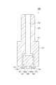
図4,5は、本実施形態に係る吸着コレットを示す図である。図4は、底面図であり、図5は、図4のV−V線に沿っての断面図である。図4,5に示されるように、吸着コレット100は、本体部110と、延在部120と、一対の接触部130と、を備えている。ここでは、本体部110、延在部120、及び接触部130は、互いに一体に形成されているが、互いに別体に構成されて接合されてもよい。
4 and 5 are diagrams showing the adsorption collet according to the present embodiment. FIG. 4 is a bottom view, and FIG. 5 is a cross-sectional view taken along the line VV of FIG. As shown in FIGS. 4 and 5, the
本体部110は、例えば直方体状を呈している。本体部110は、表面111と、表面111と反対側の表面112とを有している。延在部120は、表面111から突出するように表面111に設けられ、表面111に交差する方向に沿って延在している。延在部120は、例えば、表面111に交差する方向からみて、本体部110の一辺の長さよりも短い直径を有する円柱状であり、表面111の外縁よりも内側に配置されている。これにより、表面111は、外形が矩形状であり、且つ、内縁が円形状の環状を呈している。延在部120は、例えば、吸着コレット100を駆動するための装置(不図示)に吸着コレット100を接続する際に用いることができる。
The
表面112は、ファブリペロー干渉フィルタ1の外形に対応した形状であって、例えば矩形状(一例として正方形状)である。接触部130は、表面112から突出するように表面112に設けられている。接触部130は、ファブリペロー干渉フィルタ1を吸着する際にファブリペロー干渉フィルタ1に接触する部分である。本体部110、延在部120、及び、接触部130には、本体部110、延在部120、及び、接触部130の全長にわたって延在するように吸気孔140が設けられている。吸気孔140は、接触部130における表面112と反対側の表面(後述する接触面131)に開口すると共に、延在部120における本体部110と反対側の端部に開口している。吸気孔140は、延在部120側の開口を介して、ポンプ等の吸気装置(不図示)に接続され得る。なお、吸気孔140は、本体部110及び延在部120の全長にわたって延在するように設けられていなくてもよい。例えば、吸気孔140は、本体部110の外側面(表面112に交差する面)に至って開口を形成していてもよい。さらには、吸気孔140は、本体部110に至らず、接触部130の外側面(後述する接触面131に交差する面)に至って開口を形成していてもよい。この場合、吸気孔140は、本体部110や接触部130の外側面の開口を介して吸気装置に接続され得る。
The
接触部130は、互いに対向すると共に互いに離間して配置されている。表面112に交差(直交)する方向からみたときの接触部130の形状は、一例として、矩形の1つの角部を内側に凸となる円弧状とした形状を呈している。ここでは、接触部130は、互いの対向する側のエッジ130eが円弧状とされている。吸気孔140は、接触部130における開口(吸気のための開口)141のそれぞれから表面111に向かって延びると共に、本体部110内において1つに接続されて一体化され、延在部120に至っている。したがって、吸気孔140の延在部120側の開口は1つである。
The
ここで、吸着コレット100は、一対のガイド部150をさらに備えている。ガイド部150は、表面112から突出するように表面112に設けられている。ガイド部150は、互いに対向すると共に互いに離間して配置されている。より具体的には、ガイド部150は、接触部130の対向する方向に交差する軸線上に配置されている。表面112に交差(直交)する方向からみたときのガイド部150の形状は、一例として、L字状である。ガイド部150は、接触部130の対向する方向の軸線に対して対称となるように、互いに180°向きを変えて配置されている。ここでは、ガイド部150は、一対のガイド部150によって1つの矩形(正方形)が規定されるように配置されている。
Here, the
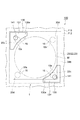
図6は、図4,5に示された吸着コレットがファブリペロー干渉フィルタを吸着した状態を示す模式図である。図6は、底面図(表面112側からみた図)であり、ファブリペロー干渉フィルタの一部を簡略化して破線で示している。図5,6に示されるように、接触部130の表面112と反対側の表面は、端子15に接触する接触面(第1接触面)131とされている。接触面131は、接触部130の配置に応じて、端子15に対応するように互いに離間して配置され、端子15のそれぞれに接触する。ここでは、接触面131は、端子15の頂面15sに接触する。ここでは、吸気孔140の開口141は、接触面131のそれぞれに1つずつ設けられている。
FIG. 6 is a schematic view showing a state in which the adsorption collet shown in FIGS. 4 and 5 adsorbs the Fabry-Perot interference filter. FIG. 6 is a bottom view (viewed from the
接触面131と端子15(頂面15s)とが接触した状態(以下、単に「接触状態」という場合がある)において、開口141は、端子15と部分的にオフセットする。より具体的には、ここでは、開口141は円形であって、その中心が、端子15の対向する方向の軸線上において端子15の外側(メンブレン構造部Mと反対側)にオフセットしている。これにより、開口141における接触部130が互いに対向する側の一部が端子15に重複しつつ、開口141の反対側の残部が端子15から逸れることになる。なお、接触状態においては、表面112と主面20sとは、互いに対向し、且つ、互いに略平行となる。なお、上記の例においては、開口141の中心が端子15の外側にオフセットした場合について例示した。しかしながら、開口141の中心が端子15の中心よりも外側であり、且つ、端子15から外れない程度にオフセットすることにより、開口141の一部が端子15に重複しつつ残部が端子15から逸れる場合もある。また、ここでのオフセットとは、ずれが生じている(ずれている)ことを意味する。
In a state where the
上述したように、接触部130のエッジ130eは、円弧状とされている。これにより、接触状態において、接触部130のメンブレン構造部M側に位置するエッジ130e、及び、接触面131のメンブレン構造部M側のエッジ131eは、メンブレン構造部Mの外側に位置し、且つ、メンブレン構造部Mの外形に沿うように形成されている。ここでは、エッジ130e,131eは、メンブレン構造部Mの外縁に倣うように円弧状に形成されている(すなわち、メンブレン構造部Mの外縁に対応する形状に形成されている)。
As described above, the
ガイド部150は、接触状態において、積層構造部20における端子15が設けられた角部20cと別の角部20dの外側において当該角部20dに沿うように設けられている。より具体的には、ガイド部150は、接触状態において、角部20dの外縁に沿うようにL字状に屈曲して延在している。ここでは、ガイド部150は、接触状態において、表面112及び主面20sに交差(直交)する方向からみて、被覆部33のさらに外側に位置し、薄化部34b内に配置される。
The
ここでは、ガイド部150の表面112からの高さは、接触部130の表面112からの高さ(表面112と接触面131との間の距離)と略同一である。したがって、接触状態においては、ガイド部150は、積層構造部20及びファブリペロー干渉フィルタ1に接触しない。ただし、ガイド部150の表面112からの高さは、接触状態において、ガイド部150の表面112と反対側の面が、薄化部34bの底面(表面)に接触しない範囲において、接触部130の表面112からの高さよりも高くてもよい。この場合、接触状態において、ガイド部150が、主面20sに沿って積層構造部20に重複するようにすることができる。
[吸着方法の実施形態]
Here, the height of the
[Embodiment of adsorption method]
引き続いて、以上の吸着コレット100を用いてファブリペロー干渉フィルタ1を吸着する吸着方法の一実施形態について説明する。図7は、本実施形態に係る吸着方法の工程を示す模式的な断面図である。図7においては、第1積層体22及び第2積層体24の層構造、及び電極等を省略している。この方法においては、まず、図7の(a)に示されるように、ファブリペロー干渉フィルタ1に対して吸着コレット100を配置する(第1工程)。この第1工程においては、積層構造部20(及びメンブレン構造部M)の主面20sに吸着コレット100の本体部110の表面112が対向するように、且つ、接触面131のそれぞれが端子15のそれぞれに対向するように、吸着コレット100を配置する。
Subsequently, an embodiment of an adsorption method for adsorbing the Fabry-
続いて、図7の(b)に示されるように、吸着コレット100をファブリペロー干渉フィルタ1に接触させる(第2工程)。この第2工程においては、接触面131のそれぞれを端子15のそれぞれに接触させる。特に、ここでは、接触面131を端子15の頂面15sに接触させる。これにより、表面112と主面20sとの間に空間Rが形成される。図6に示されるように、エッジ131eがメンブレン構造部Mの外側に位置し、且つ、メンブレン構造部Mの外縁に沿うようになる。また、図6,7に示されるように、開口141が端子15と部分的にオフセットする。さらに、積層構造部20における端子15が設けられた角部20cと別の角部20dの外側においてガイド部150が角部20dに沿うことになる。これらは、吸着コレット100の構造、及び、第1工程での相対的な配置によって実現される。
Subsequently, as shown in FIG. 7B, the
すなわち、第1工程においては、接触状態において、接触面131のエッジ131eがメンブレン構造部Mの外側に位置すると共に、メンブレン構造部Mの外縁に沿うように吸着コレット100を配置することになる。また、第1工程においては、接触状態において、開口141が端子15と部分的にオフセットするように、且つ、積層構造部20における端子15が設けられた角部20cと別の角部20dの外側においてガイド部150が角部20dに沿うように、吸着コレット100を配置することになる。
That is, in the first step, in the contact state, the
続く工程においては、接触面131の開口141を介した吸気により端子15のそれぞれを接触面131に吸着することにより、吸着コレット100によってファブリペロー干渉フィルタ1を吸着する。これにより、開口141を介した吸気を解除するまで、吸着コレット100によってファブリペロー干渉フィルタ1が吸着保持された状態が維持される。その後、必要に応じて、吸着コレット100ごと、ファブリペロー干渉フィルタ1を所定の位置まで搬送した後に、開口141を介した吸気を解除し、吸着コレット100からファブリペロー干渉フィルタ1を脱離させる。
In the subsequent step, the Fabry-
以上説明したように、本実施形態に係る吸着方法の吸着対象となるファブリペロー干渉フィルタ1は、基板11と基板11上に設けられた積層構造部20とを備えている。積層構造部20には、空隙Sを介して互いに対向し且つ互いの距離が可変とされた第1ミラー部31及び第2ミラー部32を有するメンブレン構造部Mと、主面20sに交差(直交)する方向からみてメンブレン構造部Mを挟んで互いに対向するように配置された一対の端子15と、が設けられている。これに対して、この吸着方法に用いる吸着コレット100においては、本体部110の表面112に突設された接触部130が、吸気のための開口141が形成された接触面131を含む。そして、第1工程においては、ファブリペロー干渉フィルタ1の主面20sに吸着コレット100の表面112が対向するように吸着コレット100を配置する。このとき、接触面131のそれぞれが端子15のそれぞれに対向するようにする。続いて、第2工程においては、吸着コレット100をファブリペロー干渉フィルタ1に接触させる。このとき、接触面131のそれぞれを端子15のそれぞれに接触させる。そして、第3工程においては、吸着コレット100によってファブリペロー干渉フィルタ1を吸着する。このとき、接触面131の開口141を介した吸気により端子15のそれぞれを接触面131に吸着する。これにより、ファブリペロー干渉フィルタの吸着に際して、端子15といった限定的な範囲を吸着することが可能となる。よって、適度な吸着が得られる結果、吸着を解除した際にファブリペロー干渉フィルタ1を安定して脱離させることが可能となる。
As described above, the Fabry-
また、吸着コレット100においては、端子15は、主面20sから突出した頂面15sを含む。そして、第2工程においては、接触面131を頂面15sに接触させる。このため、第2工程において、接触部130の接触面131を、メンブレン構造部Mよりも突出した端子15に接触させることになる。したがって、吸着の際に、吸着コレット100がメンブレン構造部Mに接触しないか、接触したとしてもメンブレン構造部Mへの負荷が低減される。よって、ファブリペロー干渉フィルタ1の吸着に際して、メンブレン構造部Mの破損が避けられ、ファブリペロー干渉フィルタ1の不良品の発生が抑制される。
Further, in the
また、吸着コレット100においては、接触面131が端子15に接触した状態において、接触部130及び接触面131におけるメンブレン構造部M側に位置するエッジ130e,131eは、メンブレン構造部Mの外縁に対応する形状に形成されている。そして、第1工程においては、接触面131が端子15に接触した状態において、エッジ130e,131eが、メンブレン構造部Mの外側に位置し、且つ、メンブレン構造部Mの外形に沿うように、吸着コレット100を配置する。このため、ファブリペロー干渉フィルタ1の吸着に際して、メンブレン構造部Mへの接触を避けることができる。
Further, in the
特に、吸着コレット100においては、主面20sに交差(直交)する方向からみて、メンブレン構造部Mは円形状を呈しており、エッジ130e,131eは、メンブレン構造部Mの外縁に倣うように円弧状に形成されている。このため、ファブリペロー干渉フィルタ1の吸着に際して、メンブレン構造部Mへの接触を確実に避けることができる。
In particular, in the
また、吸着方法においては、第1工程において、吸気孔140の接触面131における開口141が、接触面131が端子15に接触した状態において端子15と部分的にオフセットするように、吸着コレット100を配置する。このため、吸着力が過度に大きくなることが避けられ、ファブリペロー干渉フィルタ1をより安定して脱離させることが可能となる。
Further, in the suction method, in the first step, the
また、吸着コレット100は、一方の接触面131から他方の接触面131に向かう方向に交差する軸線上において、表面112から突出するように表面112に設けられたガイド部150を備えている。端子15は、それぞれ、主面20sに交差(直交)する方向からみて積層構造部20の角部20cに設けられている。そして、第1工程においては、ガイド部150が、接触状態において積層構造部20における端子15が設けられた角部20cと別の角部20dの外側において別の角部20dに沿うように、吸着コレット100を配置する。このため、ガイド部150によってファブリペロー干渉フィルタ1の姿勢の変化が規制され、安定した保持及び脱離が可能となる。
Further, the
さらに、吸着コレット100においては、ガイド部150は、接触面131が端子15に接触した状態において、角部20dの外縁に沿うように屈曲して延在している。このため、ガイド部150によって、主面20sに沿った平面内におけるファブリペロー干渉フィルタ1の回転が規制され、より安定した保持及び脱離が可能となる。
[変形例]
Further, in the
[Modification example]
以上の実施形態は、本発明に係る吸着方法の一実施形態を説明したものである。したがって、本発明に係る吸着方法は、上述した方法に限定されず、上述した吸着コレット100を任意に変形したものを用いた方法とすることができる。引き続いて、吸着コレットの変形例について説明する。
The above-described embodiment describes one embodiment of the adsorption method according to the present invention. Therefore, the adsorption method according to the present invention is not limited to the above-mentioned method, and a method using an arbitrarily modified
図8は、変形例に係る吸着コレットがファブリペロー干渉フィルタを吸着した状態を示す模式図である。図8は底面図(表面112側からみた図)であり、ファブリペロー干渉フィルタの一部を簡略化して破線で示している。図8に示されるように、この例では、吸着コレット100は、ガイド部150を備えていない。このように、吸着コレット100は、メンブレン構造部Mを挟んで互いに対向する一対の端子15を吸着するように構成すれば、ガイド部150を設けなくても安定した吸着・保持が可能である。なお、吸着コレット100においては、メンブレン構造部Mを挟んで互いに対向する一対の端子15,16を吸着するように構成してもよい。
FIG. 8 is a schematic view showing a state in which the adsorption collet according to the modified example adsorbs the Fabry-Perot interference filter. FIG. 8 is a bottom view (viewed from the
図9は、別の変形例に係る吸着コレットがファブリペロー干渉フィルタを吸着した状態を示す模式図である。図9は底面図(表面112側からみた図)であり、ファブリペロー干渉フィルタの一部を簡略化して破線で示している。図9に示されるように、この例では、吸着コレット100は、表面112から突出するように表面112に設けられた一対の接触部160をさらに備えている。接触部160は、一方の接触面131から他方の接触面131に向かう方向に交差する軸線上に配置されている。接触部160は、接触状態において、積層構造部20における角部20dに対応する位置に配置される。
FIG. 9 is a schematic view showing a state in which the adsorption collet according to another modification adsorbs the Fabry-Perot interference filter. FIG. 9 is a bottom view (viewed from the
接触部160は、それぞれ、端子16に対応するように配置され、端子16に接触する接触面(第2接触面)161を含む。接触面161は、互いに離間している。吸気孔140は、この接触面161にさらに開口している(吸気のための開口141が設けられている)。接触面161においても、開口141は、接触状態において、端子16と部分的にオフセットするように配置される。この吸着コレット100を用いる場合、吸着方法の第1工程においては、接触面161のそれぞれが端子16のそれぞれにさらに対向するように吸着コレット100を配置する。また、第2工程においては、接触面161のそれぞれを端子16のそれぞれにさらに接触させる。そして、第3工程においては、接触面161の開口141を介した吸気により端子16のそれぞれを接触面161にさらに吸着する。この変形例によれば、互いに位置の異なる少なくとも3点(ここでは4点)に配置された開口141を介した吸着が可能となり、ファブリペロー干渉フィルタ1をより安定して吸着・保持することが可能となる。
Each of the
なお、図9の例では、接触部130,160、及び、接触面131,161は、表面112に交差(直交)する方向からみて、矩形状に形成されている。つまり、ここでは、接触部130,160の互いに対向する側(接触状態におけるメンブレン構造部M側)のエッジ130e,160e、及び、接触面131,161の互いに対向する側(接触状態におけるメンブレン構造部M側)のエッジ131e,161eは、円弧状といったような、メンブレン構造部Mの外形に沿うような形状とされていない。このような場合であっても、接触面131,161が端子15,16の頂面15s,16sに接触するため、メンブレン構造部Mへの接触が避けられるか、接触したとしてもメンブレン構造部Mへの負荷が低減される。
In the example of FIG. 9, the
なお、図6や図8に示される例においても、図9のような形状の接触部130及び接触面131を採用してもよい。さらには、接触部130,160及び接触面131,161の形状を別の任意の形状としてもよい。
In the examples shown in FIGS. 6 and 8, the
以上の実施形態について、以下に付記する。 The above embodiments will be added below.
[付記1]
基板と、前記基板上に設けられ、前記基板と反対側に臨む主面を含む積層構造部と、を備えるファブリペロー干渉フィルタを吸着するための吸着コレットであって、
表面を有する本体部と、
前記表面から突出するように前記表面に設けられ、一対の第1接触面を含む接触部と、
を備え、
前記積層構造部には、空隙を介して互いに対向し且つ互いの距離が可変とされた第1ミラー部及び第2ミラー部と前記主面の一部とを含むメンブレン構造部と、前記主面に交差する方向からみて前記メンブレン構造部を挟んで互いに対向するように配置された一対の第1電極端子と、が設けられており、
前記本体部及び前記接触部には、前記本体部及び前記接触部にわたって延在する吸気孔が形成されており、
前記第1接触面は、前記第1電極端子のそれぞれに対応するように互いに離間して配置され、前記第1電極端子のそれぞれに接触し、
前記吸気孔は、前記第1接触面のそれぞれに開口している、
吸着コレット。
[付記2]
前記第1電極端子は、前記主面から突出した頂面を含み、
前記第1接触面は、前記頂面に接触する、
付記1に記載の吸着コレット。
[付記3]
前記第1接触面が前記第1電極端子に接触した状態において、前記接触部及び前記第1接触面における前記メンブレン構造部側に位置するエッジは、前記メンブレン構造部の外側に位置し、且つ、前記メンブレン構造部の外形に沿うように形成されている、
付記1又は2に記載の吸着コレット。
[付記4]
前記主面に交差する方向からみて、前記メンブレン構造部は円形状を呈しており、
前記エッジは、前記メンブレン構造部の外縁に倣うように円弧状に形成されている、
付記3に記載の吸着コレット。
[付記5]
前記吸気孔の前記第1接触面における開口は、前記第1接触面が前記第1電極端子に接触した状態において、前記第1電極端子と部分的にオフセットしている、
付記1〜4のいずれか一項に記載の吸着コレット。
[付記6]
一方の前記第1接触面から他方の前記第1接触面に向かう方向に交差する軸線上において、前記表面から突出するように前記表面に設けられたガイド部を備え、
前記第1電極端子は、それぞれ、前記主面に交差する方向からみて前記積層構造部の角部に設けられており、
前記ガイド部は、前記第1接触面が前記第1電極端子に接触した状態において、前記積層構造部における前記第1電極端子が設けられた角部と別の角部の外側において前記別の角部に沿うように設けられている、
付記1〜5のいずれか一項に記載の吸着コレット。
[付記7]
前記ガイド部は、前記第1接触面が前記第1電極端子に接触した状態において、前記別の角部の外縁に沿うように屈曲して延在している、
付記6に記載の吸着コレット。
[付記8]
前記ファブリペロー干渉フィルタは、前記主面に交差する方向からみて前記メンブレン構造部を挟んで互いに対向するように配置された一対の第2電極端子を備え、
前記第2電極端子は、前記第1電極端子の対向する方向に交差する軸線上に配置され、
前記接触部は、前記第2電極端子に対応するように配置され、前記第2電極端子に接触する第2接触面を含み、
前記吸気孔は、前記第2接触面にさらに開口している、
付記1〜7のいずれか一項に記載の吸着コレット。
[Appendix 1]
A suction collet for sucking a Fabry-Perot interference filter including a substrate and a laminated structure portion provided on the substrate and including a main surface facing the opposite side of the substrate.
The main body with a surface and
A contact portion provided on the surface so as to protrude from the surface and includes a pair of first contact surfaces.
With
The laminated structure portion includes a membrane structure portion including a first mirror portion and a second mirror portion and a part of the main surface facing each other through a gap and having a variable distance from each other, and the main surface. A pair of first electrode terminals arranged so as to face each other across the membrane structure portion when viewed from the direction of intersection with the above are provided.
An intake hole extending over the main body and the contact is formed in the main body and the contact.
The first contact surfaces are arranged apart from each other so as to correspond to each of the first electrode terminals, and come into contact with each of the first electrode terminals.
The intake holes are open to each of the first contact surfaces.
Adsorption collet.
[Appendix 2]
The first electrode terminal includes a top surface protruding from the main surface.
The first contact surface is in contact with the top surface.
The adsorption collet according to
[Appendix 3]
In a state where the first contact surface is in contact with the first electrode terminal, the contact portion and the edge of the first contact surface located on the membrane structure side are located outside the membrane structure and It is formed along the outer shape of the membrane structure.
The adsorption collet according to
[Appendix 4]
The membrane structure has a circular shape when viewed from the direction intersecting the main surface.
The edge is formed in an arc shape so as to imitate the outer edge of the membrane structure.
The adsorption collet according to Appendix 3.
[Appendix 5]
The opening of the intake hole at the first contact surface is partially offset from the first electrode terminal in a state where the first contact surface is in contact with the first electrode terminal.
The adsorption collet according to any one of
[Appendix 6]
A guide portion provided on the surface so as to project from the surface is provided on an axis intersecting in a direction from one of the first contact surfaces to the other of the first contact surfaces.
Each of the first electrode terminals is provided at a corner portion of the laminated structure portion when viewed from a direction intersecting the main surface.
In a state where the first contact surface is in contact with the first electrode terminal, the guide portion has the other corner outside the corner portion provided with the first electrode terminal in the laminated structure portion and another corner portion. It is provided along the part,
The adsorption collet according to any one of
[Appendix 7]
The guide portion is bent and extends along the outer edge of the other corner portion in a state where the first contact surface is in contact with the first electrode terminal.
The adsorption collet according to Appendix 6.
[Appendix 8]
The Fabry-Perot interference filter includes a pair of second electrode terminals arranged so as to face each other across the membrane structure when viewed from a direction intersecting the main surface.
The second electrode terminal is arranged on an axis intersecting the opposite directions of the first electrode terminal.
The contact portion is arranged so as to correspond to the second electrode terminal, and includes a second contact surface that contacts the second electrode terminal.
The intake hole is further open to the second contact surface.
The adsorption collet according to any one of
1…ファブリペロー干渉フィルタ、11…基板、15…端子(第1電極端子)、16…端子(第2電極端子)、20…積層構造部、20s…主面、20c…角部、20d…角部(別の角部)、31…第1ミラー部、32…第2ミラー部、100…吸着コレット、110…本体部、112…表面、130,160…接触部、131…接触面(第1接触面)、150…ガイド部、161…接触面(第2接触面)、140…吸気孔、141…開口、M…メンブレン構造部。 1 ... Fabry-Perot interference filter, 11 ... Substrate, 15 ... Terminal (first electrode terminal), 16 ... Terminal (second electrode terminal), 20 ... Laminated structure, 20s ... Main surface, 20c ... Square, 20d ... Square Part (another corner part), 31 ... 1st mirror part, 32 ... 2nd mirror part, 100 ... suction collet, 110 ... main body part, 112 ... surface, 130, 160 ... contact part, 131 ... contact surface (first Contact surface), 150 ... Guide portion, 161 ... Contact surface (second contact surface), 140 ... Intake hole, 141 ... Opening, M ... Membrane structure portion.
Claims (8)
前記主面に対向するように前記吸着コレットを配置する第1工程と、
前記第1工程の後に、前記吸着コレットを前記ファブリペロー干渉フィルタに接触させる第2工程と、
前記第2工程の後に、前記吸着コレットによって前記ファブリペロー干渉フィルタを吸着する第3工程と、
を備え、
前記吸着コレットは、表面を有する本体部と、前記表面から突出するように前記表面に設けられ、吸気のための開口が形成された一対の第1接触面を含む接触部と、を備え、
前記積層構造部には、空隙を介して互いに対向し且つ互いの距離が可変とされた第1ミラー部及び第2ミラー部と前記主面の一部とを含むメンブレン構造部と、前記主面に交差する方向からみて前記メンブレン構造部を挟んで互いに対向するように配置された一対の第1電極端子と、が設けられており、
前記第1工程においては、前記表面が前記主面に対向すると共に、前記第1接触面のそれぞれが前記第1電極端子のそれぞれに対向するように前記吸着コレットを配置し、
前記第2工程においては、前記第1接触面のそれぞれを前記第1電極端子のそれぞれに接触させ、
前記第3工程においては、前記第1接触面の前記開口を介した吸気により前記第1電極端子のそれぞれを前記第1接触面に吸着する、
吸着方法。 A adsorption method in which a Fabry-Perot interference filter including a substrate and a laminated structure portion provided on the substrate and including a main surface facing the opposite side of the substrate is adsorbed using an adsorption collet.
The first step of arranging the adsorption collet so as to face the main surface, and
After the first step, a second step of bringing the adsorption collet into contact with the Fabry-Perot interference filter, and
After the second step, the third step of adsorbing the Fabry-Perot interference filter by the adsorption collet and
With
The suction collet includes a main body portion having a surface and a contact portion including a pair of first contact surfaces provided on the surface so as to project from the surface and formed an opening for intake air.
The laminated structure portion includes a membrane structure portion including a first mirror portion and a second mirror portion and a part of the main surface facing each other through a gap and having a variable distance from each other, and the main surface. A pair of first electrode terminals arranged so as to face each other across the membrane structure portion when viewed from the direction of intersection with the above are provided.
In the first step, the adsorption collet is arranged so that the surface faces the main surface and each of the first contact surfaces faces each of the first electrode terminals.
In the second step, each of the first contact surfaces is brought into contact with each of the first electrode terminals.
In the third step, each of the first electrode terminals is adsorbed to the first contact surface by the intake air through the opening of the first contact surface.
Adsorption method.
前記第2工程においては、前記第1接触面を前記頂面に接触させる、
請求項1に記載の吸着方法。 The first electrode terminal includes a top surface protruding from the main surface.
In the second step, the first contact surface is brought into contact with the top surface.
The adsorption method according to claim 1.
前記第1工程においては、前記第1接触面が前記第1電極端子に接触した状態において、前記エッジが前記メンブレン構造部の外側に位置し、且つ、前記メンブレン構造部の外縁に沿うように、前記吸着コレットを配置する、
請求項1又は2に記載の吸着方法。 When the first contact surface is in contact with the first electrode terminal, the edge of the first contact surface located on the membrane structure side is formed in a shape corresponding to the outer edge of the membrane structure.
In the first step, in a state where the first contact surface is in contact with the first electrode terminal, the edge is located outside the membrane structure portion and is along the outer edge of the membrane structure portion. Place the adsorption collet,
The adsorption method according to claim 1 or 2.
前記エッジは、前記メンブレン構造部の外縁に倣うように円弧状に形成されている、
請求項3に記載の吸着方法。 The membrane structure has a circular shape when viewed from the direction intersecting the main surface.
The edge is formed in an arc shape so as to imitate the outer edge of the membrane structure.
The adsorption method according to claim 3.
請求項1〜4のいずれか一項に記載の吸着方法。 In the first step, the suction collet is arranged so that the opening is partially offset from the first electrode terminal in a state where the first contact surface is in contact with the first electrode terminal.
The adsorption method according to any one of claims 1 to 4.
前記第1電極端子は、それぞれ、前記主面に交差する方向からみて前記積層構造部の角部に設けられており、
前記第1工程においては、前記第1接触面が前記第1電極端子に接触した状態において、前記積層構造部における前記第1電極端子が設けられた角部と別の角部の外側において前記ガイド部が前記別の角部に沿うように、前記吸着コレットを配置する、
請求項1〜5のいずれか一項に記載の吸着方法。 The suction collet includes a guide portion provided on the surface so as to project from the surface on an axis intersecting in a direction from one of the first contact surfaces to the other of the first contact surfaces.
Each of the first electrode terminals is provided at a corner portion of the laminated structure portion when viewed from a direction intersecting the main surface.
In the first step, in a state where the first contact surface is in contact with the first electrode terminal, the guide is outside the corner portion provided with the first electrode terminal in the laminated structure portion and another corner portion. The suction collet is arranged so that the portion is along the other corner portion.
The adsorption method according to any one of claims 1 to 5.
請求項6に記載の吸着方法。 The guide portion is bent and extends along the outer edge of the other corner portion in a state where the first contact surface is in contact with the first electrode terminal.
The adsorption method according to claim 6.
前記第2電極端子は、前記第1電極端子の対向する方向に交差する軸線上に配置され、
前記接触部は、前記第2電極端子に対応するように配置されると共に吸気のための開口が形成された第2接触面を含み、
前記第1工程においては、前記第2接触面のそれぞれが前記第2電極端子のそれぞれに対向するように前記吸着コレットを配置し、
前記第2工程においては、前記第2接触面のそれぞれを前記第2電極端子のそれぞれに接触させ、
前記第3工程においては、前記第2接触面の前記開口を介した吸気により前記第2電極端子のそれぞれを前記第2接触面に吸着する、
請求項1〜7のいずれか一項に記載の吸着方法。 The Fabry-Perot interference filter includes a pair of second electrode terminals arranged so as to face each other across the membrane structure when viewed from a direction intersecting the main surface.
The second electrode terminal is arranged on an axis intersecting the opposite directions of the first electrode terminal.
The contact portion includes a second contact surface that is arranged so as to correspond to the second electrode terminal and has an opening for intake air.
In the first step, the adsorption collet is arranged so that each of the second contact surfaces faces each of the second electrode terminals.
In the second step, each of the second contact surfaces is brought into contact with each of the second electrode terminals.
In the third step, each of the second electrode terminals is adsorbed to the second contact surface by the intake air through the opening of the second contact surface.
The adsorption method according to any one of claims 1 to 7.
Priority Applications (8)
| Application Number | Priority Date | Filing Date | Title |
|---|---|---|---|
| JP2017221853A JP6899314B2 (en) | 2017-11-17 | 2017-11-17 | Adsorption method |
| CN201880073818.2A CN111357092B (en) | 2017-11-17 | 2018-11-09 | Adsorption method |
| PCT/JP2018/041726 WO2019098141A1 (en) | 2017-11-17 | 2018-11-09 | Suctioning method |
| FIEP18879718.7T FI3712930T3 (en) | 2017-11-17 | 2018-11-09 | Suctioning method |
| EP18879718.7A EP3712930B1 (en) | 2017-11-17 | 2018-11-09 | Suctioning method |
| KR1020207015943A KR102558845B1 (en) | 2017-11-17 | 2018-11-09 | adsorption method |
| US16/763,859 US11947140B2 (en) | 2017-11-17 | 2018-11-09 | Suctioning method |
| TW107140701A TWI774875B (en) | 2017-11-17 | 2018-11-16 | adsorption method |
Applications Claiming Priority (1)
| Application Number | Priority Date | Filing Date | Title |
|---|---|---|---|
| JP2017221853A JP6899314B2 (en) | 2017-11-17 | 2017-11-17 | Adsorption method |
Publications (2)
| Publication Number | Publication Date |
|---|---|
| JP2019096641A JP2019096641A (en) | 2019-06-20 |
| JP6899314B2 true JP6899314B2 (en) | 2021-07-07 |
Family
ID=66539757
Family Applications (1)
| Application Number | Title | Priority Date | Filing Date |
|---|---|---|---|
| JP2017221853A Active JP6899314B2 (en) | 2017-11-17 | 2017-11-17 | Adsorption method |
Country Status (8)
| Country | Link |
|---|---|
| US (1) | US11947140B2 (en) |
| EP (1) | EP3712930B1 (en) |
| JP (1) | JP6899314B2 (en) |
| KR (1) | KR102558845B1 (en) |
| CN (1) | CN111357092B (en) |
| FI (1) | FI3712930T3 (en) |
| TW (1) | TWI774875B (en) |
| WO (1) | WO2019098141A1 (en) |
Family Cites Families (24)
| Publication number | Priority date | Publication date | Assignee | Title |
|---|---|---|---|---|
| DE3463227D1 (en) * | 1984-08-03 | 1987-05-27 | Loh Kg Optikmaschf | Supporting device for vulnerable objects, in particular optical lenses and other optical elements |
| JPH0181633U (en) * | 1987-11-21 | 1989-05-31 | ||
| JP2514798Y2 (en) * | 1989-12-13 | 1996-10-23 | 松下電器産業株式会社 | Semiconductor chip suction device |
| JPH04188840A (en) * | 1990-11-22 | 1992-07-07 | Toshiba Corp | Die bonding method |
| FR2832512B1 (en) | 2001-11-16 | 2004-01-02 | Atmel Grenoble Sa | TUNABLE OPTICAL FILTER COMPONENT |
| JP2004157292A (en) * | 2002-11-06 | 2004-06-03 | Sharp Corp | Device for conveying liquid crystal array substrate and method for manufacturing liquid crystal display device using the same |
| TW200412616A (en) | 2003-01-08 | 2004-07-16 | Nikon Corp | Exposure device, exposure method, method of making devices, measuring method and measuring device |
| JP4270457B2 (en) | 2004-03-10 | 2009-06-03 | 大日本スクリーン製造株式会社 | Organic substance removing device and film thickness measuring device |
| JP4541807B2 (en) * | 2004-09-03 | 2010-09-08 | Okiセミコンダクタ株式会社 | Semiconductor element holding device and semiconductor element transport method |
| EP1975720A4 (en) | 2005-12-09 | 2010-05-05 | Nikon Corp | Laser light source device, exposure method, and device |
| JP2007294781A (en) | 2006-04-27 | 2007-11-08 | Shinkawa Ltd | Bonding apparatus, and method for sucking circuit board in the same |
| JP2008053306A (en) * | 2006-08-22 | 2008-03-06 | Ito Denshi Kogyo Kk | Manufacturing method of module and of camera module |
| JP2008159644A (en) | 2006-12-21 | 2008-07-10 | Shinkawa Ltd | Bonding apparatus, and method of suction for circuit board in bonding apparatus |
| FI20095976A0 (en) | 2009-09-24 | 2009-09-24 | Valtion Teknillinen | Micromechanically adjustable Fabry-Perot interferometer and method for its production |
| WO2013050243A1 (en) | 2011-10-06 | 2013-04-11 | Asml Netherlands B.V. | Chuck, lithography apparatus and method of using a chuck |
| KR101422350B1 (en) | 2012-10-31 | 2014-07-23 | 세메스 주식회사 | Method of mounting a collet to a pickup head |
| JP6260080B2 (en) * | 2013-01-07 | 2018-01-17 | セイコーエプソン株式会社 | Wavelength variable interference filter, method for manufacturing wavelength variable interference filter, optical module, and electronic device |
| JP6466851B2 (en) * | 2013-10-31 | 2019-02-06 | 浜松ホトニクス株式会社 | Photodetector |
| JP6290594B2 (en) | 2013-10-31 | 2018-03-07 | 浜松ホトニクス株式会社 | Photodetector |
| JP6356427B2 (en) | 2014-02-13 | 2018-07-11 | 浜松ホトニクス株式会社 | Fabry-Perot interference filter |
| JP6268483B2 (en) * | 2014-06-03 | 2018-01-31 | 旭硝子株式会社 | Laminate peeling apparatus, peeling method, and electronic device manufacturing method |
| JP7039160B2 (en) * | 2016-03-09 | 2022-03-22 | 浜松ホトニクス株式会社 | Photodetector |
| JP6341959B2 (en) * | 2016-05-27 | 2018-06-13 | 浜松ホトニクス株式会社 | Manufacturing method of Fabry-Perot interference filter |
| JP7348069B2 (en) * | 2017-11-17 | 2023-09-20 | 浜松ホトニクス株式会社 | Adsorption method |
-
2017
- 2017-11-17 JP JP2017221853A patent/JP6899314B2/en active Active
-
2018
- 2018-11-09 US US16/763,859 patent/US11947140B2/en active Active
- 2018-11-09 WO PCT/JP2018/041726 patent/WO2019098141A1/en unknown
- 2018-11-09 EP EP18879718.7A patent/EP3712930B1/en active Active
- 2018-11-09 CN CN201880073818.2A patent/CN111357092B/en active Active
- 2018-11-09 FI FIEP18879718.7T patent/FI3712930T3/en active
- 2018-11-09 KR KR1020207015943A patent/KR102558845B1/en active IP Right Grant
- 2018-11-16 TW TW107140701A patent/TWI774875B/en active
Also Published As
| Publication number | Publication date |
|---|---|
| EP3712930A1 (en) | 2020-09-23 |
| EP3712930B1 (en) | 2023-10-18 |
| KR20200085813A (en) | 2020-07-15 |
| CN111357092A (en) | 2020-06-30 |
| FI3712930T3 (en) | 2023-12-20 |
| TWI774875B (en) | 2022-08-21 |
| KR102558845B1 (en) | 2023-07-25 |
| CN111357092B (en) | 2023-07-07 |
| EP3712930A4 (en) | 2021-08-11 |
| US11947140B2 (en) | 2024-04-02 |
| TW201923960A (en) | 2019-06-16 |
| US20210364681A1 (en) | 2021-11-25 |
| WO2019098141A1 (en) | 2019-05-23 |
| JP2019096641A (en) | 2019-06-20 |
Similar Documents
| Publication | Publication Date | Title |
|---|---|---|
| JP2023115036A (en) | adsorption method | |
| US9611142B2 (en) | Method for manufacturing electronic component | |
| TWI738839B (en) | Fabry-Peru Interference Filter | |
| US20190186994A1 (en) | Fabry-perot interference filter | |
| JP6885338B2 (en) | Piezoelectric vibration device | |
| JP6899314B2 (en) | Adsorption method | |
| JP7470158B2 (en) | Transportation method | |
| KR102659311B1 (en) | Adsorption method | |
| JP4883077B2 (en) | Semiconductor device and manufacturing method thereof | |
| JP7154487B2 (en) | Package structure and manufacturing method thereof | |
| KR20240052898A (en) | Suction method | |
| JP4555068B2 (en) | Method for manufacturing crystal resonator package | |
| CN115021707A (en) | Vibration device | |
| JP2016072345A (en) | Mems device and mems device manufacturing method | |
| JP2016072336A (en) | Mems device and mems device manufacturing method | |
| JP2007294820A (en) | Semiconductor device and manufacturing method thereof | |
| JP2008185374A (en) | Manufacturing method of sensor device | |
| JP2007263761A (en) | Manufacturing method of sensor device |
Legal Events
| Date | Code | Title | Description |
|---|---|---|---|
| A621 | Written request for application examination |
Free format text: JAPANESE INTERMEDIATE CODE: A621 Effective date: 20201019 |
|
| TRDD | Decision of grant or rejection written | ||
| A01 | Written decision to grant a patent or to grant a registration (utility model) |
Free format text: JAPANESE INTERMEDIATE CODE: A01 Effective date: 20210608 |
|
| A61 | First payment of annual fees (during grant procedure) |
Free format text: JAPANESE INTERMEDIATE CODE: A61 Effective date: 20210614 |
|
| R150 | Certificate of patent or registration of utility model |
Ref document number: 6899314 Country of ref document: JP Free format text: JAPANESE INTERMEDIATE CODE: R150 |