JP6889849B2 - Conductive pattern sheet, intermediate member for conductive pattern sheet and its manufacturing method - Google Patents
Conductive pattern sheet, intermediate member for conductive pattern sheet and its manufacturing method Download PDFInfo
- Publication number
- JP6889849B2 JP6889849B2 JP2016133597A JP2016133597A JP6889849B2 JP 6889849 B2 JP6889849 B2 JP 6889849B2 JP 2016133597 A JP2016133597 A JP 2016133597A JP 2016133597 A JP2016133597 A JP 2016133597A JP 6889849 B2 JP6889849 B2 JP 6889849B2
- Authority
- JP
- Japan
- Prior art keywords
- conductor
- region
- product
- conductors
- unit
- Prior art date
- Legal status (The legal status is an assumption and is not a legal conclusion. Google has not performed a legal analysis and makes no representation as to the accuracy of the status listed.)
- Expired - Fee Related
Links
Images


Landscapes
- Laminated Bodies (AREA)
Description
本発明は、絶縁性基材上に導電体が配置された導電性パターンシートおよび導電性パターンシート用中間部材に関する。また本発明は、導電性パターンシート用中間部材の製造方法に関する。 The present invention relates to a conductive pattern sheet in which a conductor is arranged on an insulating base material and an intermediate member for the conductive pattern sheet. The present invention also relates to a method for manufacturing an intermediate member for a conductive pattern sheet.
今日、タッチパネル装置やフィルムアンテナ、デフロスター用フィルム電熱線、電気シェードなどの様々な分野において、絶縁性の基材上に電気回路などの導電体からなるパターンが配置された導電性パターンシートが広く用いられている。例えばタッチパネル装置に含まれるタッチパネルセンサは、基材と、基材のうち接触位置(接近位置)を検出し得るアクティブエリア内に形成された電極パターンと、誘電体のうちアクティブエリアの外側の非アクティブエリア(いわゆる額縁領域)に形成された額縁配線と、を有している。電極パターンは、導電性を有する材料、例えば金属酸化物から形成される。一方、額縁配線は、電極パターンからの信号をタッチパネルセンサの外部に設けられた制御回路に伝達するものであり、一般に、高い導電性を有する金属材料から形成される。 Today, in various fields such as touch panel devices, film antennas, film heating wires for defrosters, and electric shades, conductive pattern sheets in which patterns made of conductors such as electric circuits are arranged on an insulating base material are widely used. Has been done. For example, the touch panel sensor included in the touch panel device includes a base material, an electrode pattern formed in an active area capable of detecting a contact position (approaching position) of the base material, and an inactive outside the active area of the dielectric material. It has a frame wiring formed in an area (so-called frame area). The electrode pattern is formed from a conductive material, such as a metal oxide. On the other hand, the frame wiring transmits a signal from the electrode pattern to a control circuit provided outside the touch panel sensor, and is generally formed of a metal material having high conductivity.
このような導電性パターンシートを製造する方法として、はじめに、長尺状の絶縁性基材をその長手方向に搬送しながら、絶縁性基材上を長手方向に並ぶ複数の領域の各々に導電体からなるパターンを順次作製して導電性パターンシート用中間部材を製造し、その後、導電性パターンシート用中間部材を各領域毎に断裁することにより、複数の導電性パターンシートを効率的に得る、という方法が知られている。 As a method for producing such a conductive pattern sheet, first, while transporting a long insulating base material in the longitudinal direction, a conductor is formed in each of a plurality of regions arranged in the longitudinal direction on the insulating base material. A plurality of conductive pattern sheets can be efficiently obtained by sequentially producing a pattern made of the above and manufacturing an intermediate member for a conductive pattern sheet, and then cutting the intermediate member for a conductive pattern sheet for each region. The method is known.
ところで、このような導電性パターンシートの製造工程中、基材上に作製された導電体が帯電してしまうことが知られている。このような帯電は、基材搬送の際に基材と搬送用ローラとの間に摩擦が生じることや、ロール状に巻き取られた基材が巻き出される際に巻出部分がロール部分から剥離されることにより起こると考えられている。そして導電体の帯電量が大きくなると、例えば、上述の剥離の際などに放電が起こって導電体が破壊されてしまう、という不具合が生じることがある。 By the way, it is known that the conductor produced on the base material is charged during the manufacturing process of such a conductive pattern sheet. Such charging causes friction between the base material and the transport roller when the base material is conveyed, and when the base material wound in a roll shape is unwound, the unwound portion is released from the roll portion. It is believed to be caused by peeling. When the amount of charge of the conductor becomes large, for example, a problem may occur in which a discharge occurs at the time of the above-mentioned peeling and the conductor is destroyed.
このような課題を考慮し、非特許文献1には、帯電した導電体にイオン電荷を供給して導電体を電気的に中和し、除電することが提案されている。しかしながら、帯電量が大きい場合は十分に除電を行うことができず、導電体の破壊を防ぐことはできない。 In consideration of such a problem, Non-Patent Document 1 proposes to supply an ionic charge to a charged conductor to electrically neutralize the conductor and eliminate static electricity. However, when the amount of charge is large, it is not possible to sufficiently eliminate static electricity, and it is not possible to prevent the conductor from being destroyed.
本発明は、このような課題を効果的に解決し得る導電性パターンシート用中間部材およびその製造方法を提供することを目的とする。 An object of the present invention is to provide an intermediate member for a conductive pattern sheet and a method for manufacturing the same, which can effectively solve such a problem.
本発明は、長手方向に連続して複数の単位領域が設けられた絶縁性基材であって、各単位領域が製品領域と前記製品領域に隣接して設けられた非製品領域とを含み、隣り合う単位領域に設けられた非製品領域が互いに隣接している、絶縁性基材と、各単位領域内の前記製品領域に配置された第1導電体と、前記第1導電体から前記非製品領域に延びた取出導電体と、を備え、一つの単位領域の前記製品領域に配置された前記第1導電体に対応して設けられた取出導電体は、前記一つの単位領域と隣り合う他の単位領域の前記製品領域に配置された前記第1導電体に対応して設けられた取出導電体と、接続されている、導電性パターンシート用中間部材である。 The present invention is an insulating base material in which a plurality of unit regions are continuously provided in the longitudinal direction, and each unit region includes a product region and a non-product region provided adjacent to the product region. An insulating base material in which non-product regions provided in adjacent unit regions are adjacent to each other, a first conductor arranged in the product region in each unit region, and the non-product regions from the first conductor. A take-out conductor extending to the product area and provided corresponding to the first conductor arranged in the product area in one unit area is adjacent to the one unit area. It is an intermediate member for a conductive pattern sheet that is connected to a take-out conductor provided corresponding to the first conductor arranged in the product area of another unit area.
このような導電性パターンシート用中間部材によれば、他の単位領域に配置された第1導電体を互いに電気的に接続(導通)させ電位を揃えることができる。複数の第1導電体の除電を正確且つ効率的に実施することもできる。したがって、導電体の帯電に起因した導電体の破壊を効果的に回避することができる。 According to such an intermediate member for a conductive pattern sheet, the first conductors arranged in other unit regions can be electrically connected (conducted) to each other to make the potentials uniform. It is also possible to accurately and efficiently remove static electricity from a plurality of first conductors. Therefore, it is possible to effectively avoid the destruction of the conductor due to the charging of the conductor.
本発明による導電性パターンシート用中間部材において、前記第1導電体の周辺に、前記第1導電体から離間して第2導電体が配置されており、前記第2導電体は、前記取出導電体と接続されていてもよい。このような構成によれば、例えば最終製品領域外に何らかの理由で設けられた第2導電体も第1導電体に電気的に接続(導通)するので、導電体の帯電に起因した導電体の破壊をより効果的に回避することができる。 In the intermediate member for a conductive pattern sheet according to the present invention, a second conductor is arranged around the first conductor at a distance from the first conductor, and the second conductor is the take-out conductor. It may be connected to the body. According to such a configuration, for example, the second conductor provided outside the final product area for some reason is also electrically connected (conducted) to the first conductor, so that the conductor is charged due to the charging of the conductor. Destruction can be avoided more effectively.
この場合、前記一つの単位領域の前記製品領域に配置された前記第1導電体に対応して設けられた前記取出導電体は、前記一つの単位領域と隣り合う他の単位領域の前記製品領域に配置された前記第1導電体に対応して設けられた前記取出導電体と、前記第2導電体を介して、互いに接続されていてもよい。このような構成によれば、第2導電体および取出導電体の配置の自由度が向上するので、非製品領域の面積を低減することが可能となる。 In this case, the take-out conductor provided corresponding to the first conductor arranged in the product region of the one unit region is the product region of another unit region adjacent to the one unit region. The take-out conductor provided corresponding to the first conductor arranged in the above and the take-out conductor may be connected to each other via the second conductor. According to such a configuration, the degree of freedom in arranging the second conductor and the take-out conductor is improved, so that the area of the non-product region can be reduced.
本発明による導電性パターンシート用中間部材において、各単位領域内の前記製品領域に、複数の第1導電体が互いから離間して設けられ、前記複数の第1導電体の各々から前記非製品領域に、前記取出導電体が延び、各単位領域の前記製品領域に配置された前記複数の第1導電体に対応して設けられた複数の取出導電体は、前記非製品領域において互いに接続されていてもよい。このような構成によれば、一つの単位領域に配置された複数の第1導電体を互いに電気的に接続(導通)させ電位を揃えることができる。複数の第1導電体の除電を正確且つ効率的に実施することもできる。したがって、導電体の帯電に起因した導電体の破壊を効果的に回避することができる。 In the intermediate member for a conductive pattern sheet according to the present invention, a plurality of first conductors are provided in the product region within each unit region so as to be separated from each other, and the non-product is provided from each of the plurality of first conductors. The take-out conductor extends to the region, and a plurality of take-out conductors provided corresponding to the plurality of first conductors arranged in the product region of each unit region are connected to each other in the non-product region. You may be. According to such a configuration, a plurality of first conductors arranged in one unit region can be electrically connected (conducted) to each other to have the same potential. It is also possible to accurately and efficiently remove static electricity from a plurality of first conductors. Therefore, it is possible to effectively avoid the destruction of the conductor due to the charging of the conductor.
この場合、前記一つの単位領域の前記製品領域に配置された前記複数の第1導電体に対応して設けられた複数の取出導電体は、前記一つの単位領域内において互いから離間しており、前記他の単位領域まで延びて当該他の単位領域内において互いに接続されていてもよい。このような構成によれば、導電性パターンシート用中間部材を単位領域に分断することにより、一つの単位領域内に設けられた複数の第1導電体を互いから絶縁させることができる。 In this case, the plurality of take-out conductors provided corresponding to the plurality of first conductors arranged in the product area of the one unit region are separated from each other in the one unit region. , May extend to the other unit area and be connected to each other within the other unit area. According to such a configuration, by dividing the intermediate member for the conductive pattern sheet into unit regions, it is possible to insulate a plurality of first conductors provided in one unit region from each other.
あるいは、前記一つの単位領域の前記製品領域に配置された前記複数の第1導電体に対応して設けられた複数の取出導電体は、前記一つの単位領域内において互いから離間しており、当該複数の取出導電体の一部は、前記長手方向における一側から前記一つの単位領域に隣接する一側単位領域まで延びて前記一側単位領域内において互いに接続され、当該複数の取出導電体の残りは、前記長手方向における他側から前記一つの単位領域に隣接する他側単位領域まで延びて前記他側単位領域内において互いに接続されていてもよい。このような構成によれば、導電性パターンシート用中間部材を単位領域に分断することにより、一つの単位領域内に設けられた複数の第1導電体を互いから絶縁させることができる。また、取出導電体の配置の自由度が向上するので、非製品領域の面積を低減することも可能となる。 Alternatively, the plurality of take-out conductors provided corresponding to the plurality of first conductors arranged in the product area of the one unit region are separated from each other in the one unit region. A part of the plurality of extraction conductors extends from one side in the longitudinal direction to the one-side unit region adjacent to the one unit region and is connected to each other in the one-side unit region, and the plurality of extraction conductors are connected to each other. The rest of may extend from the other side in the longitudinal direction to the other side unit area adjacent to the one unit area and be connected to each other in the other side unit area. According to such a configuration, by dividing the intermediate member for the conductive pattern sheet into unit regions, it is possible to insulate a plurality of first conductors provided in one unit region from each other. Further, since the degree of freedom in arranging the take-out conductor is improved, it is possible to reduce the area of the non-product area.
また、本発明による導電性パターンシート用中間部材は、少なくとも前記製品領域を覆うように前記第1導電体上に積層された保護フィルムをさらに備えていてもよく、この場合、前記保護フィルムは、前記取出導電体の少なくとも一部分上には積層されていない。このような構成によれば、基材上に設けられた導電体の損傷を効果的に防止しながら、導電性パターンシート用中間部材を取り扱うこと、例えば当該導電体の電気的な検査を実施することが可能となる。 Further, the intermediate member for a conductive pattern sheet according to the present invention may further include a protective film laminated on the first conductor so as to cover at least the product area. In this case, the protective film may be provided. It is not laminated on at least a part of the take-out conductor. According to such a configuration, the intermediate member for the conductive pattern sheet is handled while effectively preventing damage to the conductor provided on the base material, for example, an electrical inspection of the conductor is carried out. It becomes possible.
本発明は、製品領域と前記製品領域に隣接して設けられた非製品領域とを含む絶縁性基材と、前記製品領域に互いから離間して配置された複数の第1導電体と、前記複数の第1導電体の各々から前記非製品領域に延びた複数の取出導電体と、を備え、前記複数の取出導電体は、前記非製品領域において互いに接続されている、導電性パターンシート用中間部材である。 The present invention comprises an insulating base material including a product region and a non-product region provided adjacent to the product region, a plurality of first conductors arranged apart from each other in the product region, and the above. For a conductive pattern sheet comprising a plurality of take-out conductors extending from each of the plurality of first conductors to the non-product region, and the plurality of take-out conductors are connected to each other in the non-product region. It is an intermediate member.
このような導電性パターンシート用中間部材によれば、一つの単位領域に配置された複数の第1導電体を互いに電気的に接続(導通)させ電位を揃えることができる。複数の第1導電体の除電を正確且つ効率的に実施することもできる。したがって、導電体の帯電に起因した導電体の破壊を効果的に回避することができる。 According to such an intermediate member for a conductive pattern sheet, a plurality of first conductors arranged in one unit region can be electrically connected (conducted) to each other to have the same potential. It is also possible to accurately and efficiently remove static electricity from a plurality of first conductors. Therefore, it is possible to effectively avoid the destruction of the conductor due to the charging of the conductor.
本発明は、長手方向に連続して複数の単位領域が設けられた絶縁性基材であって、各単位領域が製品領域と前記製品領域に隣接して設けられた非製品領域とを含み、隣り合う単位領域に設けられた非製品領域が互いに隣接している、絶縁性基材の前記製品領域に、第1導電体を作製する第1導電体作製工程と、前記第1導電体から前記非製品領域に延びる取出導電体を作製する取出導電体作製工程と、を備え、一つの単位領域の前記製品領域に配置された前記第1導電体に対応して設けられた取出導電体は、前記一つの単位領域と隣り合う他の単位領域の前記製品領域に配置された前記第1導電体に対応して設けられた取出導電体と、接続される、導電性パターンシート用中間部材の製造方法である。 The present invention is an insulating base material in which a plurality of unit regions are continuously provided in the longitudinal direction, and each unit region includes a product region and a non-product region provided adjacent to the product region. A first conductor manufacturing step of manufacturing a first conductor in the product region of an insulating base material in which non-product regions provided in adjacent unit regions are adjacent to each other, and the first conductor to the above. A take-out conductor manufacturing step of making a take-out conductor extending to a non-product region is provided, and the take-out conductor provided corresponding to the first conductor arranged in the product region in one unit region is provided. Manufacture of an intermediate member for a conductive pattern sheet, which is connected to a take-out conductor provided corresponding to the first conductor arranged in the product area of another unit area adjacent to the one unit area. The method.
このような導電性パターンシート用中間部材の製造方法によれば、他の単位領域に配置された複数の第1導電体を互いに電気的に接続(導通)させ電位を揃えることができる。複数の第1導電体の除電を正確且つ効率的に実施することもできる。したがって、導電体の帯電に起因した導電体の破壊を効果的に回避することができる。 According to such a method for manufacturing an intermediate member for a conductive pattern sheet, a plurality of first conductors arranged in other unit regions can be electrically connected (conducted) to each other to have the same potential. It is also possible to accurately and efficiently remove static electricity from a plurality of first conductors. Therefore, it is possible to effectively avoid the destruction of the conductor due to the charging of the conductor.
本発明による導電性パターンシート用中間部材の製造方法は、前記第1導電体の周辺に、前記第1導電体から離間して第2導電体を作製する第2導電体作製工程をさらに備え、前記第2導電体は、前記取出導電体と接続されてもよい。このような製造方法によれば、例えば最終製品領域外に何らかの理由で設けられた第2導電体も第1導電体に電気的に接続(導通)するので、導電体の帯電に起因した導電体の破壊をより効果的に回避することができる。 The method for manufacturing an intermediate member for a conductive pattern sheet according to the present invention further includes a second conductor manufacturing step for manufacturing a second conductor away from the first conductor around the first conductor. The second conductor may be connected to the take-out conductor. According to such a manufacturing method, for example, the second conductor provided outside the final product area for some reason is also electrically connected (conducted) to the first conductor, so that the conductor is caused by the charging of the conductor. Can be avoided more effectively.
この場合、前記一つの単位領域の前記製品領域に配置された前記第1導電体に対応して設けられた前記取出導電体は、前記一つの単位領域と隣り合う他の単位領域の前記製品領域に配置された前記第1導電体に対応して設けられた前記取出導電体と、前記第2導電体を介して、互いに接続されてもよい。このような製造方法によれば、第2導電体および取出導電体の配置の自由度が向上するので、非製品領域の面積を低減することが可能となる。 In this case, the take-out conductor provided corresponding to the first conductor arranged in the product region of the one unit region is the product region of another unit region adjacent to the one unit region. The take-out conductor provided corresponding to the first conductor arranged in the above and the take-out conductor may be connected to each other via the second conductor. According to such a manufacturing method, the degree of freedom in arranging the second conductor and the take-out conductor is improved, so that the area of the non-product region can be reduced.
本発明による導電性パターンシート用中間部材の製造方法において、前記第1導電体作製工程において、各単位領域内の前記製品領域に複数の第1導電体が互いから離間して作製され、前記取出導電体が前記複数の第1導電体の各々から前記非製品領域に延び、各単位領域の前記製品領域に配置された前記複数の第1導電体に対応して設けられた複数の取出導電体は、前記非製品領域において互いに接続されてもよい。このような製造方法によれば、一つの単位領域に配置された複数の第1導電体を互いに電気的に接続(導通)させ電位を揃えることができる。複数の第1導電体の除電を正確且つ効率的に実施することもできる。したがって、導電体の帯電に起因した導電体の破壊を効果的に回避することができる。 In the method for manufacturing an intermediate member for a conductive pattern sheet according to the present invention, in the first conductor manufacturing step, a plurality of first conductors are manufactured in the product region within each unit region so as to be separated from each other, and the first conductor is taken out. A plurality of take-out conductors in which a conductor extends from each of the plurality of first conductors to the non-product region and is provided corresponding to the plurality of first conductors arranged in the product region of each unit region. May be connected to each other in the non-product area. According to such a manufacturing method, a plurality of first conductors arranged in one unit region can be electrically connected (conducted) to each other to have the same potential. It is also possible to accurately and efficiently remove static electricity from a plurality of first conductors. Therefore, it is possible to effectively avoid the destruction of the conductor due to the charging of the conductor.
この場合、前記一つの単位領域の前記製品領域に配置された前記複数の第1導電体に対応して設けられた複数の取出導電体は、前記一つの単位領域内において互いから離間し、前記他の単位領域まで延びて当該他の単位領域内において互いに接続されてもよい。このような製造方法によれば、導電性パターンシート用中間部材を単位領域に分断することにより、一つの単位領域内に設けられた複数の第1導電体を互いから絶縁させることができる。 In this case, the plurality of take-out conductors provided corresponding to the plurality of first conductors arranged in the product area of the one unit region are separated from each other in the one unit region, and the said. They may extend to other unit areas and be connected to each other within the other unit areas. According to such a manufacturing method, by dividing the intermediate member for the conductive pattern sheet into unit regions, it is possible to insulate a plurality of first conductors provided in one unit region from each other.
あるいは、前記一つの単位領域の前記製品領域に配置された前記複数の第1導電体に対応して設けられた複数の取出導電体は、前記一つの単位領域内において互いから離間し、当該複数の取出導電体の一部は、前記長手方向における一側から前記一つの単位領域に隣接する一側単位領域まで延びて前記一側単位領域内において互いに接続され、当該複数の取出導電体の残りは、前記長手方向における他側から前記一つの単位領域に隣接する他側単位領域まで延びて前記他側単位領域内において互いに接続されてもよい。このような製造方法によれば、導電性パターンシート用中間部材を単位領域に分断することにより、一つの単位領域内に設けられた複数の第1導電体を互いから絶縁させることができる。また、取出導電体の配置の自由度が向上するので、非製品領域の面積を低減することも可能となる。 Alternatively, the plurality of take-out conductors provided corresponding to the plurality of first conductors arranged in the product area of the one unit region are separated from each other in the one unit region, and the plurality of conductors are separated from each other. A part of the extraction conductors of the above extends from one side in the longitudinal direction to the one-side unit region adjacent to the one unit region and is connected to each other in the one-side unit region, and the rest of the plurality of extraction conductors. May extend from the other side in the longitudinal direction to the other side unit area adjacent to the one unit area and be connected to each other within the other side unit area. According to such a manufacturing method, by dividing the intermediate member for the conductive pattern sheet into unit regions, it is possible to insulate a plurality of first conductors provided in one unit region from each other. Further, since the degree of freedom in arranging the take-out conductor is improved, it is possible to reduce the area of the non-product area.
本発明による導電性パターンシート用中間部材の製造方法は、少なくとも前記製品領域を覆うように前記第1導電体上に保護フィルムを積層する保護フィルム積層工程をさらに備えてもよく、この場合、前記保護フィルムは、前記取出導電体の少なくとも一部分上には積層されない。このような製造方法によれば、基材上に設けられた導電体の損傷を効果的に防止しながら、導電性パターンシート用中間部材を取り扱うこと、例えば当該導電体の電気的な検査を実施することが可能となる。 The method for manufacturing an intermediate member for a conductive pattern sheet according to the present invention may further include a protective film laminating step of laminating a protective film on the first conductor so as to cover at least the product area. In this case, the said The protective film is not laminated on at least a portion of the take-out conductor. According to such a manufacturing method, the intermediate member for the conductive pattern sheet is handled while effectively preventing damage to the conductor provided on the base material, for example, an electrical inspection of the conductor is carried out. It becomes possible to do.
本発明は、絶縁性基材と、前記絶縁性基材上に配置された第1導電体と、前記第1導電体から前記絶縁性基材の縁部まで延びた取出導電体と、を備えた導電性パターンシートである。 The present invention includes an insulating base material, a first conductor arranged on the insulating base material, and a take-out conductor extending from the first conductor to the edge of the insulating base material. It is a conductive pattern sheet.
このような導電性パターンシートは、上述の導電性パターンシート用中間部材の製造方法により製造された導電性パターンシート用中間部材から、所望の部分を切り出すことにより得られるものである。したがって、その製造工程中、第1導電体の除電が正確且つ効率的に実施され、導電体の帯電に起因した導電体の破壊が効果的に回避されている。したがって、このようにして得られた導電性パターンシートは、導電体の帯電に起因して導電体が破壊されている虞が少ない。 Such a conductive pattern sheet can be obtained by cutting out a desired portion from the conductive pattern sheet intermediate member manufactured by the above-mentioned method for manufacturing a conductive pattern sheet intermediate member. Therefore, during the manufacturing process, static elimination of the first conductor is performed accurately and efficiently, and destruction of the conductor due to charging of the conductor is effectively avoided. Therefore, in the conductive pattern sheet thus obtained, there is little possibility that the conductor is destroyed due to the charging of the conductor.
この場合、前記取出導電体は、前記第1導電体から前記絶縁性基材の縁部まで延び、前記取出導電体は、外部との接続に用いられる端子部を含み、前記端子部は、前記絶縁性基材の前記縁部から離間して配置されていてよい。このような導電性パターンシートでは、端支部が基材の縁部から離間しており、端部の損傷を効果的に防止することができる。 In this case, the take-out conductor extends from the first conductor to the edge of the insulating base material, the take-out conductor includes a terminal portion used for connection with the outside, and the terminal portion is the terminal portion. It may be arranged away from the edge of the insulating substrate. In such a conductive pattern sheet, the end support portion is separated from the edge portion of the base material, and damage to the end portion can be effectively prevented.
あるいは、前記絶縁性基材上に、複数の第1導電体が互いから離間して設けられ、前記複数の第1導電体の各々から前記絶縁性基材の縁部まで、前記取出導電体が互いから離間して延びていてもよい。このような導電性パターンシートは、その製造工程中、一つの単位領域に配置された複数の第1導電体を互いに電気的に接続(導通)させ電位を揃えることができる。複数の第1導電体の除電を正確且つ効率的に実施することもできる。したがって、このようにして得られた導電性パターンシートは、導電体の帯電に起因して導電体が破壊されている虞が少ない。 Alternatively, a plurality of first conductors are provided on the insulating base material at a distance from each other, and the take-out conductor is provided from each of the plurality of first conductors to the edge of the insulating base material. They may extend apart from each other. During the manufacturing process of such a conductive pattern sheet, a plurality of first conductors arranged in one unit region can be electrically connected (conducted) to each other to make the potentials uniform. It is also possible to accurately and efficiently remove static electricity from a plurality of first conductors. Therefore, in the conductive pattern sheet thus obtained, there is little possibility that the conductor is destroyed due to the charging of the conductor.
本発明によれば、導電体の帯電に起因した導電体の破壊を効果的に回避することができる。 According to the present invention, it is possible to effectively avoid the destruction of the conductor due to the charging of the conductor.
以下、図面を参照して本発明の第1の実施の形態について説明する。なお、以下では、導電性パターンシートとしてタッチパネルセンサシートを例に挙げて説明するが、本発明の導電性パターンシート用中間部材は、フィルムアンテナやデフロスター用フィルム電熱線、電気シェードなど、種々のものに適用可能である。 Hereinafter, the first embodiment of the present invention will be described with reference to the drawings. In the following, a touch panel sensor sheet will be described as an example of the conductive pattern sheet, but the intermediate member for the conductive pattern sheet of the present invention includes various materials such as a film antenna, a film heating wire for a defroster, and an electric shade. Applicable to.
また、本件明細書に添付する図面においては、図示と理解のしやすさの便宜上、適宜縮尺及び縦横の寸法比等を、実物のそれらから変更し誇張してある。 Further, in the drawings attached to the present specification, the scale, the aspect ratio, etc. are appropriately changed from those of the actual product and exaggerated for the convenience of illustration and comprehension.
本明細書において、「板」、「シート」、「フィルム」の用語は、呼称の違いのみに基づいて、互いから区別されるものではない。例えば、「シート」は板やフィルムと呼ばれ得るような部材をも含む概念であり、したがって、「導電性パターンシート」は、「導電性パターン板(基板)」や「導電性パターンフィルム」と呼ばれる部材と、呼称の違いのみにおいて区別され得ない。 In the present specification, the terms "board", "sheet", and "film" are not distinguished from each other based solely on the difference in designation. For example, a "sheet" is a concept that includes a member that can be called a plate or a film. Therefore, a "conductive pattern sheet" is referred to as a "conductive pattern plate (board)" or a "conductive pattern film". It cannot be distinguished only by the difference between the called member and the name.
タッチパネル装置およびタッチ位置検出機能付き表示装置
はじめに図1を参照して、第1の実施の形態によるタッチパネルセンサ30を備えたタッチ位置検出機能付き表示装置10について説明する。図1に示すように、タッチ位置検出機能付き表示装置10は、タッチパネルセンサ30と、液晶ディスプレイや有機ELディスプレイなどの表示装置15とを組み合わせることによって構成されている。図示された表示装置15は、フラットパネルディスプレイとして構成されている。表示装置15は、表示面16aを有した表示パネル16と、表示パネル16に接続された表示制御部(図示せず)と、を有している。表示パネル16は、映像を表示することができる表示エリアA1と、表示エリアA1を取り囲むようにして表示エリアA1の外側に配置された非表示エリア(額縁領域とも呼ばれる)A2と、を含んでいる。表示制御部は、表示されるべき映像に関する情報を処理し、映像情報に基づいて表示パネル16を駆動する。表示パネル16は、表示制御部の制御信号に基づいて、所定の映像を表示面16aに表示する。すなわち、表示装置15は、文字や図等の情報を映像として出力する出力装置としての役割を担っている。
Touch panel device and display device with touch position detection function First, with reference to FIG. 1, a
図1に示すように、タッチパネルセンサ30は、表示装置15の表示面16aに、例えば接着層(図示せず)を介して接着されている。
As shown in FIG. 1, the
タッチパネルセンサ
次に図2を参照して、タッチパネルセンサ30について説明する。図2は、観察者側から見た場合のタッチパネルセンサ30を示す平面図である。
Touch panel sensor Next, the
ここでは、タッチパネルセンサ30が、投影型の静電容量結合方式のタッチパネルセンサとして構成される例について説明する。なお、「容量結合」方式は、タッチパネルの技術分野において「静電容量」方式や「静電容量結合」方式等とも呼ばれており、本件では、これらの「静電容量」方式や「静電容量結合」方式等と同義の用語として取り扱う。典型的な静電容量結合方式のタッチパネルセンサは、透光性を有する導電性のパターンを有しており、外部の導体(典型的には人間の指)がタッチパネルセンサに接近することにより、外部の導体とタッチパネルセンサの導電性のパターンとの間でコンデンサ(静電容量)が形成される。そして、このコンデンサの形成に伴った電気的な状態の変化に基づき、タッチパネルセンサ上において外部導体が接近している位置の位置座標が特定される。
Here, an example in which the
図2に示すように、タッチパネルセンサ30は、観察者側を向く一側面32aおよび表示装置側を向く他側面32bを含む、透光性を有する絶縁性基材32を備えている。また、タッチパネルセンサ30は、導電性のパターンとして、絶縁性基材32の一側面32a上に設けられ、第1方向D1に延びる複数の一側第1導電体41と、絶縁性基材32の他側面32b上に設けられ、第1方向に直交する第2方向D2に延びる複数の他側第1導電体46と、を備えている。図2に示すように、一側第1導電体41および他側第1導電体46はそれぞれ帯状に延びている。また、複数の一側第1導電体41は一定の配列ピッチで第2方向D2に並べられており、複数の他側第1導電体46も一定の配列ピッチで第1方向D1に並べられている。通常は、第2方向D2における一側第1導電体41の配列ピッチと、第1方向D1における他側第1導電体46の配列ピッチとは同一になっている。一側第1導電体41および他側第1導電体46の配列ピッチは、タッチ位置の検出に関して求められる分解能に応じて定められるが、例えば数mmになっている。なお図2においては、絶縁性基材32の一側面32a側に設けられている構成要素が実線で表され、絶縁性基材32の他側面32b側に設けられている構成要素が点線で表されている。
As shown in FIG. 2, the
図1に示すように、タッチパネルセンサ30の絶縁性基材32は、タッチ位置を検出され得る領域に対応する矩形状のアクティブエリアAa1と、アクティブエリアAa1の周辺に位置する矩形枠状の非アクティブエリアAa2と、を含んでいる。図1に示された例では、アクティブエリアAa1および非アクティブエリアAa2はそれぞれ、表示パネル16の表示エリアA1および非表示エリアA2に対応して区画されている。
As shown in FIG. 1, the insulating
上述の一側第1導電体41および他側第1導電体46は、アクティブエリアAa1内に配置されている。また非アクティブエリアAa2のうち絶縁性基材32の一側面32a上には、各一側第1導電体41に電気的に接続された複数の一側取出配線43と、絶縁性基材32の外縁近傍に配置され、各一側取出配線43に電気的に接続された複数の一側端子部44と、が設けられている。さらに、非アクティブエリアAa2のうち絶縁性基材32の他側面32b上には、各他側第1導電体46に電気的に接続された複数の他側取出配線48と、絶縁性基材32の外縁近傍に配置され、各他側取出配線48に電気的に接続された複数の他側端子部49と、が設けられている。複数の取出配線46,48は、互いから離間して配置されている。複数の端子部44,49は、互いから離間して配置されている。
The one-side
一側第1導電体41に接続されている一側取出配線43および一側端子部44、並びに、他側第1導電体46に接続されている他側取出配線48および他側端子部49は一側第1導電体41並びに他側第1導電体46からの信号をタッチパネルセンサ30の外部に取り出すために設けられたものである。信号を適切に伝達することができる限りにおいて、一側取出配線43および一側端子部44並びに他側取出配線48および他側端子部49の具体的な構成が特に限られることはない。例えば取出配線43,48および端子部49は、第1導電体41,46を構成する導線と同一の層構成で当該導線と同時に形成されるものであってもよい。
The one-sided take-out
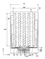
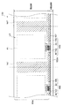
このようなタッチパネルセンサ30を作成する前段階として、図3に示すようなタッチパネルセンサシート用中間部材130が作製される。以下、図3を参照して、第1の実施の形態のタッチパネルセンサシート用中間部材130について説明する。
As a preliminary step for producing such a
(絶縁性基材)
本実施の形態のタッチパネルセンサシート用中間部材130は、長尺状の絶縁性基材132を備えている。絶縁性基材132は、タッチパネルセンサ30において誘電体として機能する絶縁性基材32の元材となるものである。絶縁性基材132を構成する材料としては、例えば、ポリエチレンテレフタレート(PET)、シクロオレフィンポリマー(COP)やガラスなど、十分な透光性を有する材料が用いられる。
( Insulating base material )
The
なお、絶縁性基材132は、上述の第1導電体41,46や取出配線43,48、端子部44,49を適切に保持することができる限りにおいて、その具体的な構成が特に限られることはない。例えば絶縁性基材132は、タッチパネルセンサ30における光の反射率や透過率を調整するためのインデックスマッチング層をさらに含んでいてもよい。他にも、PET層などの表面に設けられたハードコート層がさらに絶縁性基材132に含まれていてもよい。すなわち本実施の形態において、絶縁性基材132とは、何らかの具体的な構造や材料を意味するものではなく、タッチパネルセンサ30を構成する第1導電体41,46や端子部44,49などのパターンの下地となる絶縁性基材32の元材となるものを意味するに過ぎない。
The specific configuration of the insulating
絶縁性基材132には、絶縁性基材132の長手方向に連続して複数の単位領域U1,U2,U3が設けられている。各単位領域U1,U2,U3の長手方向に沿った長さ(幅)Wuは、製造されるタッチパネルセンサ30の幅Wに応じて規定される。
The insulating
単位領域U1,U2,U3は、各々、絶縁性基材132の長手方向に対して一方の側に、上述の第1導電体41,46や取出配線43,48、端子部44,49が配置される製品領域P1,P2,P3を含んでいる。隣り合う単位領域U1およびU2に設けられた製品領域P1およびP2は、互いに隣接しており、また、隣り合う単位領域U2およびU3に設けられた製品領域P2およびP3は、互いに隣接している。
In each of the unit regions U1, U2, and U3, the above-mentioned
各製品領域P1,P2,P3は、タッチパネルセンサ30のアクティブエリアAa1および非アクティブエリアAa2からなる領域に対応する最終製品領域F1,F2,F3を含んでいる。すなわち、最終製品領域F1,F2,F3は、一つのタッチパネルセンサを形成するようになる領域である。したがって、最終製品領域F1,F2,F3の縁部F1e,F2e,F3eは、タッチパネルセンサ30の絶縁性基材32の縁部32eに対応する。最終製品領域F1,F2,F3は、製品領域P1,P2,P3の一部分をなしている。隣り合う単位領域U1およびU2に設けられた最終製品領域F1およびF2は、互いから離間しており、また、隣り合う単位領域U2およびU3に設けられた最終製品領域F2およびF3は、互いから離間している。
Each product area P1, P2, P3 includes a final product area F1, F2, F3 corresponding to an area including an active area Aa1 and an inactive area Aa2 of the
さらに、単位領域U1,U2,U3は、各々、絶縁性基材132の長手方向に対して製品領域P1,P2,P3とは異なる側に、製品領域P1,P2,P3に隣接して設けられた非製品領域M1,M2,M3を含んでいる。絶縁性基材132は、製品領域P1,P2,P3と非製品領域M1,M2,M3とからなっており、言い換えると、製品領域P1,P2,P3と非製品領域M1,M2,M3に区分けされる。隣り合う単位領域U1およびU2に設けられた非製品領域M1およびM2は、互いに隣接しており、また隣り合う単位領域U2およびU3に設けられた非製品領域M2およびM3は、互いに隣接している。
Further, the unit regions U1, U2, and U3 are respectively provided on the side different from the product regions P1, P2, and P3 in the longitudinal direction of the insulating
(第1導電体)
絶縁性基材132の一側面132a上において、各単位領域U1,U2,U3の製品領域P1,P2,P3には、上述の一側第1導電体41が配置されている。より詳しくは、一側第1導電体41は、絶縁性基材132の一側面132a上において、製品領域P1,P2,P3の最終製品領域F1,F2,F3に配置されている。本実施の形態では、上述の複数の一側第1導電体41は、絶縁性基材132の幅方向に沿って延びており、絶縁性基材132の長手方向に互いから離間して並べられている。
( 1st conductor )
On one
図示を省略するが、絶縁性基材132の他側面132b上において、各単位領域U1,U2,U3の製品領域P1,P2,P3には、上述の他側第1導電体46が配置されている。より詳しくは、他側第1導電体46は、絶縁性基材132の他側面132b上において、製品領域P1,P2,P3の最終製品領域F1,F2,F3に、一側第1導電体41に対応して配置されている。本実施の形態では、上述の複数の他側第1導電体46は、絶縁性基材132の長手方向に沿って延びており、絶縁性基材132の幅方向に互いから離間して並べられている。
Although not shown, the above-mentioned other side
一側第1導電体41および他側第1導電体46は、例えば、遮光性および導電性を有する網目状に配置された導線から構成されている。導線の線幅は、表示装置15からの映像光が適切な透過率でタッチパネルセンサ30のアクティブエリアAa1を透過することができる限りにおいて自由に設定されるが、例えば1〜10μmの範囲内、より好ましくは2〜7μmの範囲内に設定されている。これによって、観察者が視認する映像に対して導線が及ぼす影響を、無視可能な程度まで低くすることができる。導線の厚みは、一側第1導電体41および他側第1導電体46に対して求められる電気抵抗値などに応じて適宜設定されるが、例えば0.1〜3.0μmの範囲内となっている。ただし、各第1導電体41,46が、網目状に配列された金属細線ではなく、酸化インジウム錫(ITO)等からなる透明な導電体の膜として形成されていてもよい。
The
(取出導電体)
絶縁性基材132の一側面132a上には、各単位領域U1,U2,U3に配置された一側第1導電体41から延びる一側取出導電体140が設けられている。
(Take- out conductor )
On one
本実施の形態では、一側取出導電体140は、各一側第1導電体41に接続された複数の一側取出配線43と、各一側取出配線43に接続された複数の一側端子部44とを含む導電体である。
In the present embodiment, the one-sided take-out
また、図示を省略するが、絶縁性基材132の他側面132b上には、各単位領域U1,U2,U3に配置された他側第1導電体46から延びる他側取出導電体が設けられている。
Further, although not shown, on the
本実施の形態では、他側取出導電体は、各他側第1導電体46に接続された複数の他側取出配線48と、各他側取出配線48に接続された複数の他側端子部49とを含む導電体である。
In the present embodiment, the other-side take-out conductor includes a plurality of other-side take-out
ところで、このようなタッチパネルセンサシート用中間部材130の製造は、長尺状の絶縁性基材132をその長手方向に搬送しながら、各単位領域U1,U2,U3に上述の導電体を順次作製することにより行われる。このような製造方法の場合、絶縁性基材132上に作製された導電体が帯電してしまうことが知られている。このような帯電は、絶縁性基材132の搬送の際に、絶縁性基材132と搬送用ローラとの間に摩擦が生じることや、ロール状に巻き取られた絶縁性基材132が巻き出される際に巻出部分がロール部分から剥離されることにより起こると考えられている。そして導電体の帯電量が大きくなると、例えば上述の剥離の際などに放電が起こって導電体が破壊されてしまう、という不具合が生じて、歩留まりを低下させてしまうことになる。
By the way, in the production of such an
導電体の帯電に起因する導電体の破壊を防止するために、帯電した導電体にイオン電荷を供給して導電体を電気的に中和し、除電することが提案されているが、帯電量が大きい場合は十分に除電を行うことができない。また、導電体をアースと接続することにより除電することも考えられるが、基材の搬送、巻出しおよび巻取りを伴うこのような導電性パターンシート用中間部材の製造工程においては、基材上に独立して作製された導電体の各々をアースと接続することは実質的に不可能である。 In order to prevent the conductor from being destroyed due to the charging of the conductor, it has been proposed to supply an ionic charge to the charged conductor to electrically neutralize the conductor and eliminate the charge. If is large, it is not possible to sufficiently eliminate static electricity. It is also conceivable to eliminate static electricity by connecting the conductor to the ground, but in the manufacturing process of such an intermediate member for a conductive pattern sheet, which involves transporting, unwinding, and winding the base material, the base material is used. It is virtually impossible to connect each of the independently produced conductors to ground.
このような課題を考慮して、本実施の形態では、上述の取出導電体は、絶縁性基材132の一側面132aおよび他側面132bの各々において、第1導電体から非製品領域に延びており、一つの単位領域の製品領域に配置された第1導電体に対応して設けられた取出導電体は、当該一つの単位領域と隣り合う他の単位領域の製品領域に配置された第1導電体に対応して設けられた取出導電体と、接続されている。また図示された例において、上述の取出導電体は、絶縁性基材132の一側面132aおよび他側面132bの各々において、第1導電体から最終製品領域外の領域に延び入っており、一つの単位領域の最終製品領域に配置された第1導電体に対応して設けられた取出導電体は、当該一つの単位領域と隣り合う他の単位領域の最終製品領域に配置された第1導電体に対応して設けられた取出導電体と、接続されている。
In consideration of such a problem, in the present embodiment, the above-mentioned take-out conductor extends from the first conductor to the non-product region on each of the one
具体的には、図4に示すように、本実施の形態の一側取出導電体140は、一側取出配線43および一側端子部44の他に、その一端が一側端子部44に接続された一側延長配線142aを含んでいる。一側延長配線142aは、一側面132a上を、最終製品領域F1,F2,F3内から非製品領域M1,M2,M3内に延び入っている。複数の一側延長配線142aは、互いから離間して配置されている。本実施の形態の一側取出導電体140は、また、一側面132a上において非製品領域M1,M2,M3に配置された一側接続部145を含んでいる。図示された例において、絶縁性基材132の長手方向に沿って複数の非製品領域M1,M2,M3に渡って延びている。一側接続部145には、一側延長配線142aの他端が接続されている。言い換えると、図示された一側接続部145は、互いから離間して設けられた複数の一側延長配線142aを電気的に接続している。これにより、一つの単位領域の製品領域(最終製品領域)に互いから離間して設けられた複数の第1導電体41は、共通の一側接続部145によって電気的に接続されている。また、図示された一側接続部145は、隣り合う単位領域の製品領域(最終製品領域)に対応して設けられた第1導電体41を電気的に接続している。
Specifically, as shown in FIG. 4, the one-sided take-out
図示を省略するが、本実施の形態の他側取出導電体も、他側取出配線48および他側端子部49の他に、その一端が他側端子部49に接続された他側延長配線142bを含んでおり、他側延長配線142bは、他側面132b上を非製品領域M1,M2,M3に延びている。本実施の形態の他側取出導電体は、また、他側面132b上において非製品領域M1,M2,M3に配置された他側接続部であって、絶縁性基材132の長手方向に沿って複数の非製品領域M1,M2,M3に渡って延びる他側接続部を含んでおり、他側接続部には、他側延長配線142bの他端が接続されている。
Although not shown, the other side take-out conductor of the present embodiment also has the other
これにより、複数の単位領域に独立して配置された第1導電体や取出導電体が、全体として電気的に接続(連続)した導電体のパターンを形成し、パターン内の電位を均一にすることが可能である。この結果、一部の導電体の耐電量が増大し、当該導電体が放電により破壊されてしまう、ということが効果的に回避され得る。また、複数の領域の導電体が連続したパターンを形成していることにより、複数の領域に形成された導電体をアースと接続して除電することが容易である。 As a result, the first conductors and the take-out conductors independently arranged in the plurality of unit regions form a pattern of electrically connected (continuous) conductors as a whole, and make the potential in the pattern uniform. It is possible. As a result, it can be effectively avoided that the electric charge resistance of some of the conductors increases and the conductors are destroyed by the electric discharge. Further, since the conductors in the plurality of regions form a continuous pattern, it is easy to connect the conductors formed in the plurality of regions to the ground to eliminate static electricity.
なお、一側延長配線142aや一側接続部145は、絶縁性基材132の一側面132a上の複数の単位領域に独立して配置された導電体を接続して、全体として電気的に接続(連続)した導電体のパターンとし、当該パターン内の電位を均一にするために設けられたものである。パターン内の電位の均一化が適切になされる限りにおいて、一側延長配線142aや一側接続部145の具体的な構成が特に限られることはない。例えば一側延長配線142aや一側接続部145は、一側取出配線43や一側端子部44を構成する導線と同一の層構成で当該導線と同時に形成されるものであってもよい。同様に、他側延長配線142bおよび一側接続部は、他側取出配線43や他側端子部49を構成する導線と同一の層構成で当該導線と同時に形成されるものであってもよい。
The one-
(第2導電体)
本実施の形態では、絶縁性基材132の一側面132a上において、一側第1導電体41の周辺に、一側第1導電体41から離間して一側第2導電体147が配置されている。一側第2導電体147は、位置検出以外の目的で配置される配線である。例えば、一側第2導電体147は、一側第1導電体41や一側取出配線43、一側検査電極44、一側延長配線142a、一側接続部145を作製するためのエッチング工程において、エッチングが絶縁性基材の面内において均一に行われるよう、エッチング液に溶け出した金属の濃度を面内で均一にするために配置される導電体(配線部)である。したがって、これらの導電体の作製が適切になされる限りにおいて、一側第2導電体147の具体的な構成が特に限られることはない。例えば一側第2導電体147は、一側第1導電体41を構成する導線と同一の層構成で当該導線と同時に形成されるものであってもよい。また、一側第2導電体147は、タッチパネルセンサに必要な構成要素ではないので、絶縁性基材132の最終製品領域F1,F2,F3外の領域に形成されるようにしてもよい。
( Second conductor )
In the present embodiment, the one-sided
本実施の形態では、一側第2導電体147は、図4に示すように、一側第1導電体41の一側接続部145と接続(接触)されている。これにより、一側第2導電体147は、一側第1導電体41および一側取出導電体140と共に全体として電気的に接続(連続)したパターンを形成する。この結果、一側第2導電体147の電位を、一側第1導電体41および一側取出導電体140の電位と等しくすることが可能である。
In the present embodiment, the one-sided
図示を省略するが、本実施の形態では、絶縁性基材132の他側面132bの他側第1導電体46の周辺にも、一側第2導電体147と同様の目的で、他側第1導電体46から離間して他側第2導電体が配置されており、他側第2導電体は、他側取出導電体に接続されている。
Although not shown, in the present embodiment, the other side
(保護フィルム)
本実施の形態では、第1導電体41上には、少なくとも最終製品領域F1,F2,F3の全域を覆うように一側保護フィルム80aが積層されている。好ましくは、一側保護フィルム80aは、製品領域P1,P2,P3を覆うように設けられる。一側保護フィルム80aは、絶縁性基材132の一側面32a上に形成された一側第1導電体41や一側取出配線43、一側端子部44に他の部材が接触してキズや断線を生じることを防止するとともに、一側第1導電体41や一側取出配線43、一側端子部44に塵埃等の異物が付着することを防止するために積層されるものである。したがって、一側面32a上に配置されたこれらの導電体の保護が適切になされる限りにおいて、一側保護フィルム80aの具体的な構成が特に限られることはない。例えば、一側保護フィルム80aは、ポリエチレンテレフタレート(PET)製またはポリプロピレン(PP)製のフィルムである。
( Protective film )
In the present embodiment, the one-side
上述のように、一側保護フィルム80aは、絶縁性基材132の一側面132a上において、少なくとも製品領域P1,P2,P3を覆うように第1導電体41上に配置されるが、一側取出導電体140の少なくとも一部分上、より詳細には一側接続部145上には積層されていない。これにより、後述する一側接続部145の断裁が容易になる。
As described above, the one-side
具体的には、本実施の形態においては、一側保護フィルム80aは、長尺状の形状を有しており、その長手方向軸が絶縁性基材132の長手方向軸と平行になるように、かつ、一側面132a上において少なくとも製品領域P1,P2,P3は覆われるが一側接続部145は露出されるように、一側第1導電体41上に積層されている。
Specifically, in the present embodiment, the one-side
図示を省略するが、本実施の形態では、絶縁性基材132の他側面132bの他側第1導電体46上にも、一側保護フィルム80aと同様の目的で、一側保護フィルム80aと同様の他側保護フィルム80bが積層されている。
Although not shown, in the present embodiment, the one-side
具体的には、本実施の形態においては、他側保護フィルム80bは、長尺状の形状を有しており、その長手方向軸が絶縁性基材132の長手方向軸と平行になるように、かつ、他側面132b上において少なくとも製品領域P1,P2,P3は覆われるが他側接続部は露出されるように、他側第1導電体46上に積層されている。
Specifically, in the present embodiment, the other side
中間部材製造装置
次に、図9を参照して、本実施の形態によるタッチパネルセンサシート用中間部材130を製造するための中間部材製造装置200の構成について説明する。図9に示すように、中間部材製造装置200は、基材搬送方向Tの最も上流側に、基材供給軸202を備えている。基材供給軸202は、長尺状の絶縁性基材132がロール状に巻き取られてなる基材ロール132rが設置されるものであり、基材供給軸202を回転させることにより、基材ロール132rから絶縁性基材132を供給することができるようになっている。
Intermediate member manufacturing apparatus Next, with reference to FIG. 9, the configuration of the intermediate
基材供給軸202に対して基材搬送方向Tの下流側の各箇所には、基材搬送路を構成する送りローラ204が配置されており、基材ロール132rから供給された絶縁性基材132を支持しながら搬送することができるようになっている。
基材供給軸202に対して基材搬送方向Tの下流側には、搬送されてきた絶縁性基材132の一側面132aおよび他側面132b上に、それぞれ第1導電体41,46を作製するための第1導電体作製装置206が備えられている。第1導電体41,46の作製は、絶縁性基材132の一側面132aおよび他側面132b上に金属層を形成し、当該金属層上にレジスト層を設け、このレジスト層を露光・現像してパターニングし、レジスト層をマスクとして金属層をエッチングしてレジスト層を除去することにより行われる。金属層を設ける方法としては、例えばスパッタリング法やめっき法が用いられ得る。なお、一側第1導電体41および他側第1導電体46の作成工程の少なくとも一部分が同時に行われてもよいし、一側第1導電体41および他側第1導電体46の作成工程が順に行われるようにしてもよい。
第1導電体作製装置206に対して基材搬送方向Tの下流側には、搬送されてきた絶縁性基材132の一側面132aおよび他側面132b上に、それぞれ第2導電体を作製するための第2導電体作製装置208が備えられている。第2導電体の作製は、上述の第1導電体41,46の作製と同様に行われる。なお、第1導電体41,46および第2導電体を同一材料から作製する場合等は、共通の導電体作製装置によって、第1導電体41,46および第2導電体を同時に作製するようにしてもよい。
In order to fabricate the second conductor on one
第2導電体作製装置208に対して基材搬送方向Tの下流側には、搬送されてきた絶縁性基材132の一側面132aおよび他側面132b上に、それぞれ取出導電体を作製するための取出導電体作製装置210が備えられている。取出導電体の作製は、上述の第1導電体41,46の作製と同様に行われる。なお、取出導電体と第1導電体41,46および第2導電体のいずれかとを同一材料から作製する場合などは、共通の導電体作製装置によって、取出導電体と他の導電体とを同時に作製するようにしてもよい。
On the downstream side of the base material transporting direction T with respect to the second
取出導電体作製装置210に対して基材搬送方向Tの下流側には、導電性の一側除電ローラ212aと他側除電ローラ212bとが配置されており、搬送されてきた絶縁性基材132の一側面132aが一側除電ローラ212aに、他側面132bが他側除電ローラ212bに、各々接するようになっている。一側除電ローラ212aと他側除電ローラ212bとは、アースに接続されている。これにより、一側除電ローラ212aおよび他側除電ローラ212bの電位は、基準電位に維持されている。
A conductive one-side
一側除電ローラ212aおよび他側除電ローラ212bに対して基材搬送方向Tの下流側であって、搬送される絶縁性基材132の一側面132aの側には、一側保護フィルム供給軸214aが配置されている。一側保護フィルム供給軸214aは、一側保護フィルム80aがロール状に巻き取られてなる一側保護フィルムロール80arが設置されるものであり、一側保護フィルム供給軸214aを回転させることにより、一側保護フィルムロール80arから一側保護フィルム80aを、搬送されてきた絶縁性基材132の一側面132aに向けて供給することができるようになっている。なお、一側除電ローラ212aおよび他側除電ローラ212bの設置位置は、図示された例に限られず、また、設置数も複数としてもよい。
One side protective
また、一側除電ローラ212aおよび他側除電ローラ212bに対して基材搬送方向Tの下流側であって、搬送される絶縁性基材132の他側面132bの側には、他側保護フィルム供給軸214bが配置されている。他側保護フィルム供給軸214bは、他側保護フィルム80bがロール状に巻き取られてなる他側保護フィルムロール80brが設置されるものであり、他側保護フィルム供給軸214bを回転させることにより、他側保護フィルムロール80brから他側保護フィルム80bを、搬送されてきた絶縁性基材132の他側面132bに向けて供給することができるようになっている。
Further, the other side protective film is supplied to the side of the
一側保護フィルム供給軸214aおよび他側保護フィルム供給軸214bに対して基材搬送方向Tの下流側には、一対のニップローラ216が設けられていて、一側保護フィルムロール80arから絶縁性基材132の一側面132aに向けて供給された一側保護フィルム80aを、当該一側面132a上に、また、他側保護フィルムロール80brから絶縁性基材132の他側面132bに向けて供給された他側保護フィルム80bを、当該他側面132b上に、それぞれ押圧して積層することができるようになっている。
A pair of nip
一対のニップローラ216に対して基材搬送方向Tの下流側には、中間部材巻取軸218が設けられており、中間部材巻取軸218が回転することにより、保護フィルム80a,80bが積層された絶縁性基材132を巻き取ることができるようになっている。
An intermediate member take-up
導電性パターンシート用中間部材の製造方法
次に、このような中間部材製造装置200を用いたタッチパネルセンサシート用中間部材の製造方法について説明する。
Method for Manufacturing Intermediate Member for Conductive Pattern Sheet Next, a method for manufacturing an intermediate member for a touch panel sensor sheet using such an intermediate
はじめに、長尺状の絶縁性基材132がロール状に巻き取られてなる基材ロール132rを準備し、基材供給軸202に設置する。次に基材供給軸202を回転させ、基材ロール132rから絶縁性基材132を基材搬送路に向けて給送する。給送された絶縁性基材132rは、送りローラ204に支持されながら、金属層作製装置206に向けて搬送される。
First, a
第1導電体作製装置206において、絶縁性基材132の一側面132a上および他側面132b上に、第1導電体41,46が作製される。具体的には、絶縁性基材132の長手方向に連続して設けられた各単位領域U1,U2,U3の製品領域P1,P2,P3において、一側面132a上には複数の一側第1導電体41が互いから離間して作製され、他側面132b上には複数の他側第1導電体46が互いから離間して作製される。第1導電体作製装置206を通過した絶縁性基材132は、送りローラ204に支持されながら、第2導電体作製装置208に向けて搬送される。
In the first
第2導電体作製装置208において、絶縁性基材132の一側面132a上および他側面132b上に、第2導電体が、第1導電体41,46の周囲に、第1導電体41,46から離間して作製される。第2導電体作製装置208を通過した絶縁性基材132は、送りローラ204に支持されながら、取出導電体作製装置210に向けて搬送される。
In the second
取出導電体作製装置210において、絶縁性基材132の一側面132a上および他側面132b上に、取出導電体が作製される。具体的には、取出導電体は、各単位領域U1,U2,U3の製品領域P1,P2,P3に作製された第1導電体41,46から非製品領域M1,M2,M3に延びるように、且つ、一つの単位領域の製品領域に配置された第1導電体41,46に対応して設けられた取出導電体が当該一つの単位領域と隣り合う他の単位領域の製品領域に配置された第1導電体41,46に対応して設けられた取出導電体と接続されるように、作製される。また、取出導電体は、第2導電体と接続されるように作製される。取出導電体作製装置210を通過した絶縁性基材132は、送りローラ204に支持されながら、一側除電ローラ212aおよび他側除電ローラ212bに向けて搬送される。
In the take-out
一側除電ローラ212aおよび他側除電ローラ212bに送られた絶縁性基材132は、その一側面132aが一側除電ローラ212aに当接され、また他側面132bが他側除電ローラ212bに当接される。これによって、絶縁性基材132上に作製された全体として連続した導電体のパターンの電位は、基準電位に維持される。
In the insulating
一側除電ローラ212aおよび他側除電ローラ212bを通過した絶縁性基材132は、さらに一対のニップローラ216へ送られ、当該ニップローラ216の間を通過する。このとき、一側保護フィルム供給軸214aに設置された一側保護フィルムロール80arから供給された一側保護フィルム80aが、絶縁性基材132の一側面132a上に、製品領域P1,P2,P3を覆うように配置された状態で、絶縁性基材132と共に一対のニップローラ216の間を通過する。また、他側保護フィルム供給軸214bに設置された他側保護フィルムロール80brから供給された他側保護フィルム80bが、絶縁性基材132の他側面132b上に、製品領域P1,P2,P3を覆うように配置された状態で、絶縁性基材132と共に一対のニップローラ216の間を通過する。ただし、保護フィルム80a,80bは、取出導電体140の少なくとも一部分を覆わずに露出させている。
The insulating
絶縁性基材132と共に一対のニップローラ216の間を通過した保護フィルム80a,80bは、ニップローラ216によって絶縁性基材216に対して押圧される。これによって、一側保護フィルム80aおよび他側保護フィルム80bが、それぞれ、絶縁性基材132の一側面132a上の一側第1導電体41および他側面132b上の他側第1導電体46上に積層される。
The
そして、保護フィルム80a,80bが積層された絶縁性基材132は、中間部材巻取軸218によって巻き取られる。
Then, the insulating
以上の工程により、図5に示すタッチパネルセンサシート用中間部材130を作製することができる。
Through the above steps, the
このようにして作成されたタッチパネルセンサシート用中間部材130の非製品領域M1,M2,M3を断裁することにより、絶縁性基材132上に本来独立して作製されるべき各導電体の接続を断絶することが可能である。これにより、各単位領域U1,U2,U3に作製された導電体のパターンの動作確認検査を行うことができる。具体的には、各第1導電体41が断線していないか、また、第1導電体41同士が電気的に絶縁されているか、を電気的な検査を行うことにより確認する。
By cutting the non-product areas M1, M2, and M3 of the
あるいは、タッチパネルセンサシート用中間部材130の非製品領域M1,M2,M3の全域を断裁することに代え、図6に示すように、非製品領域M1,M2,M3の一部分のみを除去して、検査を実施することもできる。図6に示された例では、タッチパネルセンサシート用中間部材130の非製品領域M1,M2,M3のうち、接続部と延長配線142a,142bとが接続する部分を切り欠くことで、絶縁性基材132上に本来電気的に独立(絶縁)して作製されるべき各導電体の接続を断絶することが可能である。
Alternatively, instead of cutting the entire non-product area M1, M2, M3 of the
また、本実施の形態のタッチパネルセンサシート用中間部材130を単位領域U1,U2,U3毎に断裁することにより、タッチパネルセンサ用中間部材としてのタッチパネルセンサシートを得ることができる。
Further, by cutting the
さらに、製品領域P1,P2,P3から最終製品領域F1,F2,F3のみを切り出すことにより、タッチパネルセンサ30を得ることができる。このようにして得られたタッチパネルセンサ30を、表示装置15と組み合わせることによって、入出力装置10を得ることができる。この場合、端子部44,49にその一端が接続された延長配線142a,142bの一部がタッチパネルセンサ30に残ることとなる。より詳しくは、タッチパネルセンサ(導電体パターンシート)30は、複数の第1導電体41,46と、各第1導電体41,46に電気的に接続した一側取出導電体と、を有し、各取出導電体は、その一端において各第1導電体41,46に接続した取出配線43,48と、取出配線43,48の他端に接続した端子部44,49と、端子部44,49と基材32の縁部32eとの間を延びる延長配線142a,142bと、を含んでいる。延長配線142a,142bは、端子部44,49よりも幅狭となっている。このようなタッチパネルセンサ(導電体パターンシート)30では、端子部44,49が基材32の縁部32eから離間しており、端子部44,49の損傷を効果的に防止することができる。
Further, the
なお、保護フィルム80a,80bは、タッチパネルセンサ30が表示装置15と組み合わされる前の任意の時点で除去される。
The
本実施の形態によれば、上述のように、一側取出導電体140は、絶縁性基材132の一側面132a上において、一側第1導電体41から非製品領域M1,M2,M3に延びており、一つの単位領域の製品領域、例えば単位領域U1の製品領域P1、に配置された一側第1導電体41に対応して設けられた一側取出導電体43は、一つの単位領域と隣り合う他の単位領域の製品領域、例えば単位領域U1と隣り合う単位領域U2の製品領域P2、に配置された一側第1導電体41に対応して設けられた一側取出導電体43と、接続されている。また、一側第2導電体147は、一側第1導電体41の一側接続部145と接続されている。すなわち、複数の単位領域に独立して配置された第1導電体、第2導電体および取出導電体が、全体として連続した導電体のパターンを形成している。これにより、当該パターン内の電位を均一にすることができ、一部の導電体の帯電量が増大して放電し、当該導電体が破壊されてしまう、ということが効果的に回避される。
According to the present embodiment, as described above, the one-sided take-out
また、タッチパネルセンサシート用中間部材の製造中、絶縁性基材132上に作製された導電体のパターンを、アースに接続された導電性の除電ローラ212a,212bに当接させることにより、パターン内の電位を基準電位に保つことができる。これにより、導電体の帯電に起因した導電体の破壊を、さらに効果的に回避することができる。
Further, during the production of the intermediate member for the touch panel sensor sheet, the pattern of the conductor produced on the insulating
次に、本発明による導電性パターンシート用中間部材の他の実施の形態について説明する。以下の説明および以下の説明で用いる図面では、上述した実施の形態と同様に構成され得る部分について、上述の実施の形態における対応する部分に対して用いた符号と同一の符号を用いることとし、重複する説明を省略する。 Next, another embodiment of the intermediate member for the conductive pattern sheet according to the present invention will be described. In the following description and the drawings used in the following description, the same codes as those used for the corresponding parts in the above-described embodiment will be used for the parts that can be configured in the same manner as in the above-described embodiment. Duplicate explanations will be omitted.
まず、図7を参照して、本発明による導電性パターンシート用中間部材の第2の実施の形態について説明する。図7は、第2の実施の形態における、タッチパネルセンサシート用中間部材230を示す図である。
First, with reference to FIG. 7, a second embodiment of the intermediate member for the conductive pattern sheet according to the present invention will be described. FIG. 7 is a diagram showing an
本実施の形態において、一つの単位領域の製品領域に配置された第1導電体に対応して設けられた取出導電体は、一つの単位領域と隣り合う他の単位領域の製品領域に配置された第1導電体に対応して設けられた取出導電体と、第2導電体を介して互いに接続されている。第2の実施の形態は、この点において上述した第1の実施の形態と異なり、その他の点において上述した第1の実施の形態と同一とすることができる。 In the present embodiment, the take-out conductor provided corresponding to the first conductor arranged in the product area of one unit area is arranged in the product area of another unit area adjacent to one unit area. The take-out conductor provided corresponding to the first conductor and the take-out conductor are connected to each other via the second conductor. The second embodiment is different from the first embodiment described above in this respect, and can be the same as the first embodiment described above in other respects.
具体的には、本実施の形態においては、一側接続部145’は、複数の単位領域U1,U2,U3に渡って連続的に設けられておらず、各単位領域U1,U2,U3の製品領域P1,P2,P3に配置された一側第1導電体41に対応して設けられた一側延長配線142aを、各単位領域毎に接続するのみである。一方、一側第2導電体147は、絶縁性基材132の一側面132a上において、隣り合う単位領域に配置された一側接続部145’を接続するように配置されている。
Specifically, in the present embodiment, the one-side connection portion 145'is not continuously provided over the plurality of unit areas U1, U2, U3, and is provided in each unit area U1, U2, U3. Only the one-
また、本実施の形態では、図7に示すように、一つの単位領域の製品領域に配置された複数の第1導電体に対応して設けられた複数の取出導電体は、一つの単位領域内において互いから離間しており、他の単位領域まで延びて当該他の単位領域内において接続されている。 Further, in the present embodiment, as shown in FIG. 7, the plurality of extraction conductors provided corresponding to the plurality of first conductors arranged in the product area of one unit area are one unit area. They are separated from each other within and extend to other unit areas and are connected within the other unit areas.
具体的には、本実施の形態においては、図7に示すように、絶縁性基材132の一側面132a上において、例えば、単位領域U1の製品領域P1に配置された複数の一側第1導電体41に対応して設けられた一側延長配線142aは、単位領域U1から単位領域U2へ互いから離間したまま延びており、単位領域U2に配置された接続部147に接続されている。取出導電体をこのように構成することにより、タッチパネルセンサシート用中間部材130を、単位領域毎に断裁すれば、同時に、絶縁性基材132上に本来独立して作製されるべき各導電体の接続を断絶することが可能である。
Specifically, in the present embodiment, as shown in FIG. 7, a plurality of first side firsts arranged on one
本実施のタッチパネルセンサシート用中間部材230によっても、複数の単位領域に独立して配置された第1導電体、第2導電体および取出導電体が、全体として連続した導電体のパターンを形成している。これにより、当該パターン内の電位を均一にすることができ、一部の導電体の帯電量が増大して放電し、当該導電体が破壊されてしまう、ということが効果的に回避される。
Also in the
また、タッチパネルセンサシート用中間部材の製造中、絶縁性基材132上に作製された導電体のパターンを、アースに接続された導電性の除電ローラ212a,212bに当接させることにより、パターン内の電位を基準電位に保つことができる。これにより、導電体の帯電に起因した導電体の破壊を、さらに効果的に回避することができる。
Further, during the production of the intermediate member for the touch panel sensor sheet, the pattern of the conductor produced on the insulating
さらに、タッチパネルセンサシート用中間部材130を単位領域毎に断裁するだけで、絶縁性基材132上に本来独立して作製されるべき各導電体の接続を断絶することが可能である。
Further, by simply cutting the
次に、図8を参照して、本発明による導電性パターンシート用中間部材の第3の実施の形態について説明する。図8は、第3の実施の形態における、タッチパネルセンサシート用中間部材330を示す図である。
Next, a third embodiment of the intermediate member for the conductive pattern sheet according to the present invention will be described with reference to FIG. FIG. 8 is a diagram showing an
本実施の形態においても、一つの単位領域の製品領域に配置された第1導電体に対応して設けられた取出導電体は、一つの単位領域と隣り合う他の単位領域の製品領域に配置された第1導電体に対応して設けられた取出導電体と、第2導電体を介して互いに接続されている。また、一つの単位領域の製品領域に配置された複数の第1導電体に対応して設けられた複数の取出導電体は、一つの単位領域内において互いから離間している。 Also in the present embodiment, the take-out conductors provided corresponding to the first conductors arranged in the product area of one unit area are arranged in the product area of another unit area adjacent to one unit area. The take-out conductor provided corresponding to the first conductor and the take-out conductor are connected to each other via the second conductor. Further, the plurality of take-out conductors provided corresponding to the plurality of first conductors arranged in the product area of one unit area are separated from each other in one unit area.
しかし、本実施の形態においては、複数の取出導電体の一部は、絶縁性基材の長手方向における一側から一つの単位領域に隣接する一側単位領域まで延びて一側単位領域内において互いに接続され、複数の取出導電体の残りは、絶縁性基材の長手方向における他側からの一つの単位領域に隣接する他側単位領域まで延びて他側単位領域内において互いに接続されている。 However, in the present embodiment, a part of the plurality of extraction conductors extends from one side in the longitudinal direction of the insulating base material to the one-side unit region adjacent to one unit region within the one-side unit region. Connected to each other, the rest of the ejected conductors extend from the other side in the longitudinal direction of the insulating substrate to the other side unit area adjacent to one unit area and are connected to each other within the other side unit area. ..
具体的には、本実施の形態においては、図8に示すように、絶縁性基材132の一側面132a上において、例えば、単位領域U2の製品領域P2に配置された複数の一側第1導電体41に対応して設けられた一側延長配線142aのうち、単位領域U3に近い側に配置された一部の一側延長配線142rは、単位領域U3まで延びて、単位領域U3内に設けられた接続部145rに接続されている。一方、他の一側延長配線142lは、単位領域U1まで延びて、単位領域U1内に設けられた接続部145lに接続されている。
Specifically, in the present embodiment, as shown in FIG. 8, a plurality of first side firsts arranged on one
本実施のタッチパネルセンサシート用中間部材330によっても、複数の単位領域に独立して配置された第1導電体、第2導電体および取出導電体が、全体として連続した導電体のパターンを形成している。これにより、当該パターン内の電位を均一にすることができ、一部の導電体の帯電量が増大して放電し、当該導電体が破壊されてしまう、ということが効果的に回避される。
Also in the
また、タッチパネルセンサシート用中間部材の製造中、絶縁性基材132上に作製された導電体のパターンを、アースに接続された導電性の除電ローラ212a,212bに当接させることにより、パターン内の電位を基準電位に保つことができる。これにより、導電体の帯電に起因した導電体の破壊を、さらに効果的に回避することができる。
Further, during the production of the intermediate member for the touch panel sensor sheet, the pattern of the conductor produced on the insulating
さらに、タッチパネルセンサシート用中間部材130を単位領域毎に断裁するだけで、絶縁性基材132上に本来独立して作製されるべき各導電体の接続を断絶することが可能である。
Further, by simply cutting the
30 タッチパネルセンサ
32 基材
41 一側第1導電体
43 一側取出配線
44 一側端支部
46 他側第1導電体
48 他側取出配線
49 他側端支部
132 絶縁性基材
140 一側取出導電体
142a 一側延長配線
145 一側接続部
147 一側第2導電体
A1 表示エリア
A2 非表示エリア
U1 単位領域
U2 単位領域
U3 単位領域
P1 製品領域
P2 製品領域
P3 製品領域
M1 非製品領域
M2 非製品領域
M3 非製品領域
30
Claims (21)
各単位領域内の前記製品領域に配置された第1導電体と、
前記第1導電体から前記非製品領域に延びた取出導電体と、
を備え、
前記取出導電体は、前記製品領域に配置されて外部との接続に用いられる端子部と、前記端子部に接続された延長配線と、を含み、
前記端子部は、前記製品領域の縁部から離間して配置されており、
前記延長配線は、前記非製品領域に延び入っており、
一つの単位領域の前記製品領域に配置された前記第1導電体に対応して設けられた取出導電体の延長配線は、前記一つの単位領域と隣り合う他の単位領域の前記製品領域に配置された前記第1導電体に対応して設けられた取出導電体の延長配線と、接続されている導電性パターンシート用中間部材。 An insulating base material in which a plurality of unit regions are continuously provided in the longitudinal direction, and each unit region includes a product region and a non-product region provided adjacent to the product region, and adjacent unit regions are provided. With an insulating substrate in which the non-product areas provided in the are adjacent to each other,
The first conductor arranged in the product area in each unit area and
A take-out conductor extending from the first conductor to the non-product region,
With
The take-out conductor includes a terminal portion arranged in the product area and used for connection with the outside, and an extension wiring connected to the terminal portion.
The terminal portion is arranged so as to be separated from the edge portion of the product area.
The extension wiring extends into the non-product area and extends into the non-product area.
The extension wiring of the take-out conductor provided corresponding to the first conductor arranged in the product area of one unit area is arranged in the product area of another unit area adjacent to the one unit area. An intermediate member for a conductive pattern sheet that is connected to an extension wiring of a take-out conductor provided corresponding to the first conductor.
前記第2導電体は、前記取出導電体の前記延長配線と接続されている
請求項1に記載の導電性パターンシート用中間部材。 A second conductor is arranged around the first conductor at a distance from the first conductor.
The intermediate member for a conductive pattern sheet according to claim 1, wherein the second conductor is connected to the extension wiring of the take-out conductor.
請求項2に記載の導電性パターンシート用中間部材。 The extension wiring of the take-out conductor provided corresponding to the first conductor arranged in the product region of the one unit region is the product of another unit region adjacent to the one unit region. The conductive pattern according to claim 2, wherein the extension wiring of the take-out conductor provided corresponding to the first conductor arranged in the region and the conductive pattern of the take-out conductor are connected to each other via the second conductor. Intermediate member for seat.
前記複数の第1導電体の各々から前記非製品領域に、前記取出導電体が延び、
各単位領域の前記製品領域に配置された前記複数の第1導電体に対応して設けられた複数の取出導電体の延長配線は、前記非製品領域において互いに接続されている
請求項1乃至3のいずれか一項に記載の導電性パターンシート用中間部材。 A plurality of first conductors are provided apart from each other in the product area within each unit area.
The take-out conductor extends from each of the plurality of first conductors to the non-product region.
Claims 1 to 3 in which the extension wirings of the plurality of take-out conductors provided corresponding to the plurality of first conductors arranged in the product region of each unit region are connected to each other in the non-product region. The intermediate member for a conductive pattern sheet according to any one of the above.
請求項4に記載の導電性パターンシート用中間部材。 The plurality of take-out conductors provided corresponding to the plurality of first conductors arranged in the product region of the one unit region are separated from each other in the one unit region, and the plurality of conductors are separated from each other. The intermediate member for a conductive pattern sheet according to claim 4, wherein the extension wiring of the take-out conductor is extended to the other unit region and connected to each other in the other unit region.
当該複数の取出導電体の一部の延長配線は、前記長手方向における一側から前記一つの単位領域に隣接する一側単位領域まで延びて前記一側単位領域内において互いに接続され、
当該複数の取出導電体の残りの延長配線は、前記長手方向における他側から前記一つの単位領域に隣接する他側単位領域まで延びて前記他側単位領域内において互いに接続されている
請求項4に記載の導電性パターンシート用中間部材。 The plurality of take-out conductors provided corresponding to the plurality of first conductors arranged in the product area of the one unit region are separated from each other in the one unit region.
Some extension wirings of the plurality of extraction conductors extend from one side in the longitudinal direction to the one-side unit region adjacent to the one unit region and are connected to each other in the one-side unit region.
4. The remaining extension wirings of the plurality of extraction conductors extend from the other side in the longitudinal direction to the other side unit region adjacent to the one unit region and are connected to each other in the other side unit region. An intermediate member for a conductive pattern sheet according to.
をさらに備え、
前記保護フィルムは、前記取出導電体の少なくとも一部分上には積層されていない
請求項1乃至6のいずれか一項に記載の導電性パターンシート用中間部材。 A protective film laminated on the first conductor so as to cover at least the product area is further provided.
The intermediate member for a conductive pattern sheet according to any one of claims 1 to 6, wherein the protective film is not laminated on at least a part of the take-out conductor.
前記製品領域に互いから離間して配置された複数の第1導電体と、
前記複数の第1導電体の各々から前記非製品領域に延びた複数の取出導電体と、
を備え、
各取出導電体は、前記製品領域に配置されて外部との接続に用いられる端子部と、前記端子部に接続された延長配線と、を含み、
前記端子部は、前記製品領域の縁部から離間して配置されており、
前記延長配線は、前記非製品領域に延び入っており、
前記複数の取出導電体の前記延長配線は、前記非製品領域において互いに接続されている
導電性パターンシート用中間部材。 An insulating base material containing a product area and a non-product area provided adjacent to the product area,
A plurality of first conductors arranged apart from each other in the product area,
A plurality of extraction conductors extending from each of the plurality of first conductors to the non-product region,
With
Each take-out conductor includes a terminal portion arranged in the product area and used for connection with the outside, and an extension wiring connected to the terminal portion.
The terminal portion is arranged so as to be separated from the edge portion of the product area.
The extension wiring extends into the non-product area and extends into the non-product area.
The extension wiring of the plurality of take-out conductors is an intermediate member for a conductive pattern sheet connected to each other in the non-product area.
各単位領域内の前記製品領域に配置された第1導電体と、
前記第1導電体から前記非製品領域に延びた取出導電体と、
を備えた導電性パターンシート用中間部材であって、
各単位領域内の前記製品領域に、複数の第1導電体が互いから離間して設けられ、 前記複数の第1導電体の各々から前記非製品領域に、前記取出導電体が延び、 前記一つの単位領域の前記製品領域に配置された前記複数の第1導電体に対応して設けられた複数の取出導電体は、前記一つの単位領域内において互いから離間しており、前記一つの単位領域と隣り合う他の単位領域の非製品領域まで延びて当該他の単位領域の非製品領域内において互いに接続されている
導電性パターンシート用中間部材。 An insulating base material in which a plurality of unit regions are continuously provided in the longitudinal direction, and each unit region includes a product region and a non-product region provided adjacent to the product region, and adjacent unit regions are provided. With an insulating substrate in which the non-product areas provided in the are adjacent to each other,
The first conductor arranged in the product area in each unit area and
A take-out conductor extending from the first conductor to the non-product region,
It is an intermediate member for a conductive pattern sheet equipped with
A plurality of first conductors are provided in the product region within each unit region so as to be separated from each other, and the take-out conductor extends from each of the plurality of first conductors to the non-product region, and the one is described. The plurality of take-out conductors provided corresponding to the plurality of first conductors arranged in the product area of one unit region are separated from each other in the one unit region, and the one unit. An intermediate member for a conductive pattern sheet that extends to a non-product area of another unit area adjacent to the area and is connected to each other in the non-product area of the other unit area.
各単位領域内の前記製品領域に配置された第1導電体と、
前記第1導電体から前記非製品領域に延びた取出導電体と、
を備えた導電性パターンシート用中間部材であって、
各単位領域内の前記製品領域に、複数の第1導電体が互いから離間して設けられ、
前記複数の第1導電体の各々から前記非製品領域に、前記取出導電体が延び、
前記一つの単位領域の前記製品領域に配置された前記複数の第1導電体に対応して設けられた複数の取出導電体は、前記一つの単位領域内において互いから離間しており、 当該複数の取出導電体の一部は、前記長手方向における一側から前記一つの単位領域に隣接する一側単位領域の非製品領域まで延びて前記一側単位領域の非製品領域内において互いに接続され、
当該複数の取出導電体の残りは、前記長手方向における他側から前記一つの単位領域に隣接する他側単位領域の非製品領域まで延びて前記他側単位領域の非製品領域内において互いに接続されている
導電性パターンシート用中間部材。 An insulating base material in which a plurality of unit regions are continuously provided in the longitudinal direction, and each unit region includes a product region and a non-product region provided adjacent to the product region, and adjacent unit regions are provided. With an insulating substrate in which the non-product areas provided in the are adjacent to each other,
The first conductor arranged in the product area in each unit area and
A take-out conductor extending from the first conductor to the non-product region,
It is an intermediate member for a conductive pattern sheet equipped with
A plurality of first conductors are provided apart from each other in the product area within each unit area.
The take-out conductor extends from each of the plurality of first conductors to the non-product region.
A plurality of take-out conductors provided corresponding to the plurality of first conductors arranged in the product area of the one unit region are separated from each other in the one unit region, and the plurality of conductors are separated from each other. Some of the take-out conductors extend from one side in the longitudinal direction to the non-product region of the one-side unit region adjacent to the one unit region and are connected to each other within the non-product region of the one-side unit region.
The rest of the plurality of extraction conductors extends from the other side in the longitudinal direction to the non-product region of the other side unit region adjacent to the one unit region and is connected to each other in the non-product region of the other side unit region. Intermediate member for conductive pattern sheet.
前記第1導電体から前記非製品領域に延びる取出導電体を作製する取出導電体作製工程と、
を備え、
前記取出導電体は、前記製品領域に配置されて外部との接続に用いられる端子部と、前記端子部に接続された延長配線と、を含み、
前記端子部は、前記製品領域の縁部から離間して配置され、
前記延長配線は、前記非製品領域に延び入り、
一つの単位領域の前記製品領域に配置された前記第1導電体に対応して設けられた取出導電体の延長配線は、前記一つの単位領域と隣り合う他の単位領域の前記製品領域に配置された前記第1導電体に対応して設けられた取出導電体の延長配線と、接続される導電性パターンシート用中間部材の製造方法。 An insulating base material in which a plurality of unit regions are continuously provided in the longitudinal direction, and each unit region includes a product region and a non-product region provided adjacent to the product region, and adjacent unit regions are provided. A first conductor manufacturing step of manufacturing a first conductor in the product region of an insulating base material in which non-product regions provided in the above are adjacent to each other.
A take-out conductor manufacturing step of manufacturing a take-out conductor extending from the first conductor to the non-product region, and
With
The take-out conductor includes a terminal portion arranged in the product area and used for connection with the outside, and an extension wiring connected to the terminal portion.
The terminal portion is arranged so as to be separated from the edge portion of the product area.
The extension wiring extends into the non-product area and
The extension wiring of the take-out conductor provided corresponding to the first conductor arranged in the product area of one unit area is arranged in the product area of another unit area adjacent to the one unit area. A method for manufacturing an intermediate member for a conductive pattern sheet to be connected to an extension wiring of a take-out conductor provided corresponding to the first conductor.
をさらに備え、
前記第2導電体は、前記取出導電体の前記延長配線と接続される
請求項11に記載の製造方法。 A second conductor manufacturing step of manufacturing the second conductor away from the first conductor is further provided around the first conductor.
The manufacturing method according to claim 11, wherein the second conductor is connected to the extension wiring of the take-out conductor.
請求項12に記載の製造方法。 The extension wiring of the take-out conductor provided corresponding to the first conductor arranged in the product region of the one unit region is the product of another unit region adjacent to the one unit region. The manufacturing method according to claim 12, wherein the extension wiring of the take-out conductor provided corresponding to the first conductor arranged in the region and the second conductor are connected to each other.
前記取出導電体が前記複数の第1導電体の各々から前記非製品領域に延び、
各単位領域の前記製品領域に配置された前記複数の第1導電体に対応して設けられた複数の取出導電体の延長配線は、前記非製品領域において互いに接続される
請求項11乃至13のいずれか一項に記載の製造方法。 In the first conductor manufacturing step, a plurality of first conductors are manufactured in the product region within each unit region so as to be separated from each other.
The take-out conductor extends from each of the plurality of first conductors to the non-product region.
The extension wirings of the plurality of take-out conductors provided corresponding to the plurality of first conductors arranged in the product region of each unit region are connected to each other in the non-product region according to claims 11 to 13. The manufacturing method according to any one of the above.
請求項14に記載の製造方法。 A plurality of extraction conductors provided corresponding to the plurality of first conductors arranged in the product area of the one unit region are separated from each other in the one unit region, and the plurality of extraction conductors are separated from each other. The manufacturing method according to claim 14, wherein the extension wiring of the conductor extends to the other unit region and is connected to each other in the other unit region.
当該複数の取出導電体の一部の延長配線は、前記長手方向における一側から前記一つの単位領域に隣接する一側単位領域まで延びて前記一側単位領域内において互いに接続され、
当該複数の取出導電体の残りの延長配線は、前記長手方向における他側から前記一つの単位領域に隣接する他側単位領域まで延びて前記他側単位領域内において互いに接続される
請求項14に記載の製造方法。 The plurality of take-out conductors provided corresponding to the plurality of first conductors arranged in the product region of the one unit region are separated from each other in the one unit region.
Some extension wirings of the plurality of extraction conductors extend from one side in the longitudinal direction to the one-side unit region adjacent to the one unit region and are connected to each other in the one-side unit region.
14. The remaining extension wiring of the plurality of extraction conductors extends from the other side in the longitudinal direction to the other side unit region adjacent to the one unit region and is connected to each other in the other side unit region. The manufacturing method described.
をさらに備え、
前記保護フィルムは、前記取出導電体の少なくとも一部分上には積層されない
請求項11乃至16のいずれか一項に記載の製造方法。 A protective film laminating step of laminating a protective film on the first conductor so as to cover at least the product area is further provided.
The production method according to any one of claims 11 to 16, wherein the protective film is not laminated on at least a part of the take-out conductor.
前記第1導電体から前記非製品領域に延びる取出導電体を作製する取出導電体作製工程と、
を備えた導電性パターンシート用中間部材の製造方法であって、
前記第1導電体作製工程において、各単位領域内の前記製品領域に複数の第1導電体が互いから離間して作製され、
前記取出導電体が前記複数の第1導電体の各々から前記非製品領域に延び、
前記一つの単位領域の前記製品領域に配置された前記複数の第1導電体に対応して設けられた複数の取出導電体は、前記一つの単位領域内において互いから離間し、前記一つの単位領域と隣り合う他の単位領域の非製品領域まで延びて当該他の単位領域の非製品領域内において互いに接続される
導電性パターンシート用中間部材の製造方法。 An insulating base material in which a plurality of unit regions are continuously provided in the longitudinal direction, and each unit region includes a product region and a non-product region provided adjacent to the product region, and adjacent unit regions are provided. A first conductor manufacturing step of manufacturing a first conductor in the product region of an insulating base material in which non-product regions provided in the above are adjacent to each other.
A take-out conductor manufacturing step of manufacturing a take-out conductor extending from the first conductor to the non-product region, and
This is a method for manufacturing an intermediate member for a conductive pattern sheet.
In the first conductor manufacturing step, a plurality of first conductors are manufactured in the product region within each unit region so as to be separated from each other.
The take-out conductor extends from each of the plurality of first conductors to the non-product region.
A plurality of extraction conductors provided corresponding to the plurality of first conductors arranged in the product region of the one unit region are separated from each other in the one unit region, and the one unit is separated from each other. A method for manufacturing an intermediate member for a conductive pattern sheet that extends to a non-product region of another unit region adjacent to a region and is connected to each other in the non-product region of the other unit region.
前記第1導電体から前記非製品領域に延びる取出導電体を作製する取出導電体作製工程と、
を備えた導電性パターンシート用中間部材の製造方法であって、
前記第1導電体作製工程において、各単位領域内の前記製品領域に複数の第1導電体が互いから離間して作製され、
前記取出導電体が前記複数の第1導電体の各々から前記非製品領域に延び、
前記一つの単位領域の前記製品領域に配置された前記複数の第1導電体に対応して設けられた複数の取出導電体は、前記一つの単位領域内において互いから離間し、
当該複数の取出導電体の一部は、前記長手方向における一側から前記一つの単位領域に隣接する一側単位領域の非製品領域まで延びて前記一側単位領域の非製品領域内において互いに接続され、
当該複数の取出導電体の残りは、前記長手方向における他側から前記一つの単位領域に隣接する他側単位領域の非製品領域まで延びて前記他側単位領域の非製品領域内において互いに接続される
導電性パターンシート用中間部材の製造方法。 An insulating base material in which a plurality of unit regions are continuously provided in the longitudinal direction, and each unit region includes a product region and a non-product region provided adjacent to the product region, and adjacent unit regions are provided. A first conductor manufacturing step of manufacturing a first conductor in the product region of an insulating base material in which non-product regions provided in the above are adjacent to each other.
A take-out conductor manufacturing step of manufacturing a take-out conductor extending from the first conductor to the non-product region, and
This is a method for manufacturing an intermediate member for a conductive pattern sheet.
In the first conductor manufacturing step, a plurality of first conductors are manufactured in the product region within each unit region so as to be separated from each other.
The take-out conductor extends from each of the plurality of first conductors to the non-product region.
The plurality of take-out conductors provided corresponding to the plurality of first conductors arranged in the product region of the one unit region are separated from each other in the one unit region.
A part of the plurality of extraction conductors extends from one side in the longitudinal direction to the non-product region of the one-side unit region adjacent to the one unit region and connects to each other in the non-product region of the one-side unit region. Being done
The rest of the plurality of extraction conductors extends from the other side in the longitudinal direction to the non-product region of the other side unit region adjacent to the one unit region and is connected to each other in the non-product region of the other side unit region. A method for manufacturing an intermediate member for a conductive pattern sheet.
前記絶縁性基材上に配置された第1導電体と、
前記第1導電体から前記絶縁性基材の縁部まで延びた取出導電体と、
を備え、
各取出導電体は、前記第1導電体に接続された単一の取出配線と、前記取出配線に接続されて外部との接続に用いられる単一の端子部と、前記端子部と前記絶縁性基板の前記縁部との間を延びる単一の延長配線と、を含み、
前記端子部は、前記絶縁性基材の前記縁部から離間して配置されている
導電性パターンシート。 Insulating base material and
The first conductor arranged on the insulating base material and
A take-out conductor extending from the first conductor to the edge of the insulating base material,
With
Each extraction conductor, said a single take-out wirings connected to the first conductor, and a single terminal unit used for connection with the outside is connected to the take-out wiring, the insulating and the terminal portion Includes a single extension wire extending between the edges of the substrate.
The terminal portion is a conductive pattern sheet arranged apart from the edge portion of the insulating base material.
前記複数の第1導電体の各々から前記絶縁性基材の縁部まで、前記取出導電体が互いから離間して延びている
請求項20に記載の導電性パターンシート。 A plurality of first conductors are provided on the insulating base material so as to be separated from each other.
The conductive pattern sheet according to claim 20, wherein the take-out conductors extend apart from each other from each of the plurality of first conductors to the edge of the insulating base material.
Priority Applications (1)
| Application Number | Priority Date | Filing Date | Title |
|---|---|---|---|
| JP2016133597A JP6889849B2 (en) | 2016-07-05 | 2016-07-05 | Conductive pattern sheet, intermediate member for conductive pattern sheet and its manufacturing method |
Applications Claiming Priority (1)
| Application Number | Priority Date | Filing Date | Title |
|---|---|---|---|
| JP2016133597A JP6889849B2 (en) | 2016-07-05 | 2016-07-05 | Conductive pattern sheet, intermediate member for conductive pattern sheet and its manufacturing method |
Publications (2)
| Publication Number | Publication Date |
|---|---|
| JP2018001654A JP2018001654A (en) | 2018-01-11 |
| JP6889849B2 true JP6889849B2 (en) | 2021-06-18 |
Family
ID=60947193
Family Applications (1)
| Application Number | Title | Priority Date | Filing Date |
|---|---|---|---|
| JP2016133597A Expired - Fee Related JP6889849B2 (en) | 2016-07-05 | 2016-07-05 | Conductive pattern sheet, intermediate member for conductive pattern sheet and its manufacturing method |
Country Status (1)
| Country | Link |
|---|---|
| JP (1) | JP6889849B2 (en) |
Families Citing this family (5)
| Publication number | Priority date | Publication date | Assignee | Title |
|---|---|---|---|---|
| JP7212854B2 (en) * | 2018-09-25 | 2023-01-26 | 大日本印刷株式会社 | Conductive pattern substrate and method for manufacturing conductive pattern substrate |
| JP7364373B2 (en) * | 2019-07-03 | 2023-10-18 | トライベイル テクノロジーズ, エルエルシー | touch panel |
| JP2021060891A (en) * | 2019-10-09 | 2021-04-15 | パナソニックIpマネジメント株式会社 | Touch sensor intermediate body and manufacturing method thereof, inspection method of touch sensor intermediate body |
| WO2021075421A1 (en) * | 2019-10-18 | 2021-04-22 | 富士フイルム株式会社 | Touch sensor member precursor, and method for manufacturing touch sensor member |
| JP2022182674A (en) * | 2021-05-28 | 2022-12-08 | パナソニックIpマネジメント株式会社 | Pattern film, roll film, and manufacturing method of pattern film |
Family Cites Families (10)
| Publication number | Priority date | Publication date | Assignee | Title |
|---|---|---|---|---|
| JP5444967B2 (en) * | 2009-09-04 | 2014-03-19 | 大日本印刷株式会社 | Display device substrate and method of manufacturing display device substrate |
| JP5782727B2 (en) * | 2011-02-04 | 2015-09-24 | 大日本印刷株式会社 | Touch panel sensor manufacturing method and etching method |
| JP5403434B2 (en) * | 2011-06-22 | 2014-01-29 | 大日本印刷株式会社 | Touch panel sensor |
| JP5698103B2 (en) * | 2011-10-27 | 2015-04-08 | 富士フイルム株式会社 | Conductive film and touch panel |
| JP2013222590A (en) * | 2012-04-16 | 2013-10-28 | Shin Etsu Polymer Co Ltd | Conductive pattern formation substrate and manufacturing method thereof |
| KR20140038822A (en) * | 2012-09-21 | 2014-03-31 | 삼성전기주식회사 | A raw glass plate for manufacturing a touch panel and method for manufacturing touch panel using the same |
| JP6115427B2 (en) * | 2013-09-25 | 2017-04-19 | 大日本印刷株式会社 | Touch panel sensor and manufacturing method thereof |
| JP2015106240A (en) * | 2013-11-29 | 2015-06-08 | 富士フイルム株式会社 | Conductive film and touch panel |
| JP6182120B2 (en) * | 2014-08-28 | 2017-08-16 | 富士フイルム株式会社 | Transparent conductive film, method for manufacturing transparent conductive film, and touch panel |
| JP6331897B2 (en) * | 2014-09-03 | 2018-05-30 | 凸版印刷株式会社 | Touch sensor substrate |
-
2016
- 2016-07-05 JP JP2016133597A patent/JP6889849B2/en not_active Expired - Fee Related
Also Published As
| Publication number | Publication date |
|---|---|
| JP2018001654A (en) | 2018-01-11 |
Similar Documents
| Publication | Publication Date | Title |
|---|---|---|
| JP6889849B2 (en) | Conductive pattern sheet, intermediate member for conductive pattern sheet and its manufacturing method | |
| KR101973321B1 (en) | Conductive sheet and capacitive touch panel | |
| US10551949B2 (en) | Display integrated antenna | |
| JP5565709B2 (en) | Touch panel sensor, laminate for manufacturing touch panel sensor, and method for manufacturing touch panel sensor | |
| JP5078534B2 (en) | Transparent sheet and transparent touch switch | |
| CN102693036B (en) | Manufacture the method for the transparent circuit substrate being used for touch-screen | |
| US20190012026A1 (en) | Touch panel and method for manufacturing the same, display apparatus | |
| US10365689B2 (en) | Transparent cover for electronic device | |
| CN105808012A (en) | Display module and display device | |
| JP6477164B2 (en) | Intermediate member for touch panel sensor, and electrical inspection method for intermediate member for touch panel sensor | |
| US10951211B2 (en) | FPC integrated capacitance switch and method of manufacturing the same | |
| CN107430462B (en) | Method and apparatus for manufacturing thin film touch sensor | |
| WO2017045367A1 (en) | Array substrate, display panel, and display device | |
| TWI683250B (en) | Transparent electrode member, method for manufacturing the same, and electrostatic capacitance sensor using the transparent electrode member | |
| US10598828B2 (en) | Optical film laminate used for continuous lamination to panel component | |
| KR20130072402A (en) | Fabrication method of electrode-pattern of touch panel | |
| US9842862B2 (en) | Flexible electronic device with anti-interference structures and manufacturing method thereof | |
| JP2015032214A (en) | Display device with touch panel sensor and touch position detection function | |
| KR102105607B1 (en) | Capacitive sensor | |
| US20150277485A1 (en) | Input device and display device | |
| WO2017006757A1 (en) | Antenna-equipped touchscreen | |
| JP7212854B2 (en) | Conductive pattern substrate and method for manufacturing conductive pattern substrate | |
| JP2022182674A (en) | Pattern film, roll film, and manufacturing method of pattern film | |
| JP6504445B2 (en) | Intermediate member for touch panel sensor, and method of manufacturing touch panel sensor | |
| JP6205995B2 (en) | Display device with touch panel sensor and touch position detection function |
Legal Events
| Date | Code | Title | Description |
|---|---|---|---|
| A621 | Written request for application examination |
Free format text: JAPANESE INTERMEDIATE CODE: A621 Effective date: 20190530 |
|
| A977 | Report on retrieval |
Free format text: JAPANESE INTERMEDIATE CODE: A971007 Effective date: 20200226 |
|
| A131 | Notification of reasons for refusal |
Free format text: JAPANESE INTERMEDIATE CODE: A131 Effective date: 20200303 |
|
| A521 | Request for written amendment filed |
Free format text: JAPANESE INTERMEDIATE CODE: A523 Effective date: 20200507 |
|
| A131 | Notification of reasons for refusal |
Free format text: JAPANESE INTERMEDIATE CODE: A131 Effective date: 20200918 |
|
| A521 | Request for written amendment filed |
Free format text: JAPANESE INTERMEDIATE CODE: A523 Effective date: 20201116 |
|
| TRDD | Decision of grant or rejection written | ||
| A01 | Written decision to grant a patent or to grant a registration (utility model) |
Free format text: JAPANESE INTERMEDIATE CODE: A01 Effective date: 20210423 |
|
| A61 | First payment of annual fees (during grant procedure) |
Free format text: JAPANESE INTERMEDIATE CODE: A61 Effective date: 20210506 |
|
| R150 | Certificate of patent or registration of utility model |
Ref document number: 6889849 Country of ref document: JP Free format text: JAPANESE INTERMEDIATE CODE: R150 |
|
| LAPS | Cancellation because of no payment of annual fees |