JP6888362B2 - Detection device, physical quantity measuring device, detection system, electronic device and mobile body - Google Patents
Detection device, physical quantity measuring device, detection system, electronic device and mobile body Download PDFInfo
- Publication number
- JP6888362B2 JP6888362B2 JP2017060780A JP2017060780A JP6888362B2 JP 6888362 B2 JP6888362 B2 JP 6888362B2 JP 2017060780 A JP2017060780 A JP 2017060780A JP 2017060780 A JP2017060780 A JP 2017060780A JP 6888362 B2 JP6888362 B2 JP 6888362B2
- Authority
- JP
- Japan
- Prior art keywords
- detection
- data
- detection device
- common
- timing
- Prior art date
- Legal status (The legal status is an assumption and is not a legal conclusion. Google has not performed a legal analysis and makes no representation as to the accuracy of the status listed.)
- Active
Links
- 238000001514 detection method Methods 0.000 title claims description 558
- 238000012545 processing Methods 0.000 claims description 100
- 230000005540 biological transmission Effects 0.000 claims description 65
- 230000001133 acceleration Effects 0.000 claims description 31
- 238000000034 method Methods 0.000 description 30
- 230000008569 process Effects 0.000 description 18
- 238000006243 chemical reaction Methods 0.000 description 16
- 238000004891 communication Methods 0.000 description 8
- 230000000052 comparative effect Effects 0.000 description 7
- 238000012986 modification Methods 0.000 description 7
- 230000004048 modification Effects 0.000 description 7
- 230000007274 generation of a signal involved in cell-cell signaling Effects 0.000 description 6
- 230000010355 oscillation Effects 0.000 description 5
- 239000004065 semiconductor Substances 0.000 description 5
- 238000012937 correction Methods 0.000 description 4
- 230000001360 synchronised effect Effects 0.000 description 4
- 238000010586 diagram Methods 0.000 description 3
- 230000010354 integration Effects 0.000 description 3
- 238000012935 Averaging Methods 0.000 description 2
- 230000003321 amplification Effects 0.000 description 2
- 239000000470 constituent Substances 0.000 description 2
- 238000007796 conventional method Methods 0.000 description 2
- 238000013481 data capture Methods 0.000 description 2
- 230000006870 function Effects 0.000 description 2
- 230000008676 import Effects 0.000 description 2
- 230000007246 mechanism Effects 0.000 description 2
- 238000003199 nucleic acid amplification method Methods 0.000 description 2
- 208000033748 Device issues Diseases 0.000 description 1
- XUIMIQQOPSSXEZ-UHFFFAOYSA-N Silicon Chemical compound [Si] XUIMIQQOPSSXEZ-UHFFFAOYSA-N 0.000 description 1
- 239000002131 composite material Substances 0.000 description 1
- 230000003111 delayed effect Effects 0.000 description 1
- 230000000694 effects Effects 0.000 description 1
- 230000005284 excitation Effects 0.000 description 1
- 238000001914 filtration Methods 0.000 description 1
- 238000007689 inspection Methods 0.000 description 1
- 239000004973 liquid crystal related substance Substances 0.000 description 1
- 230000002093 peripheral effect Effects 0.000 description 1
- 230000035945 sensitivity Effects 0.000 description 1
- 229910052710 silicon Inorganic materials 0.000 description 1
- 239000010703 silicon Substances 0.000 description 1
- 239000000758 substrate Substances 0.000 description 1
- 239000000725 suspension Substances 0.000 description 1
- 238000012546 transfer Methods 0.000 description 1
Images


Classifications
-
- H—ELECTRICITY
- H03—ELECTRONIC CIRCUITRY
- H03B—GENERATION OF OSCILLATIONS, DIRECTLY OR BY FREQUENCY-CHANGING, BY CIRCUITS EMPLOYING ACTIVE ELEMENTS WHICH OPERATE IN A NON-SWITCHING MANNER; GENERATION OF NOISE BY SUCH CIRCUITS
- H03B5/00—Generation of oscillations using amplifier with regenerative feedback from output to input
- H03B5/30—Generation of oscillations using amplifier with regenerative feedback from output to input with frequency-determining element being electromechanical resonator
- H03B5/32—Generation of oscillations using amplifier with regenerative feedback from output to input with frequency-determining element being electromechanical resonator being a piezoelectric resonator
-
- G—PHYSICS
- G01—MEASURING; TESTING
- G01C—MEASURING DISTANCES, LEVELS OR BEARINGS; SURVEYING; NAVIGATION; GYROSCOPIC INSTRUMENTS; PHOTOGRAMMETRY OR VIDEOGRAMMETRY
- G01C19/00—Gyroscopes; Turn-sensitive devices using vibrating masses; Turn-sensitive devices without moving masses; Measuring angular rate using gyroscopic effects
- G01C19/56—Turn-sensitive devices using vibrating masses, e.g. vibratory angular rate sensors based on Coriolis forces
- G01C19/5776—Signal processing not specific to any of the devices covered by groups G01C19/5607 - G01C19/5719
-
- B—PERFORMING OPERATIONS; TRANSPORTING
- B60—VEHICLES IN GENERAL
- B60W—CONJOINT CONTROL OF VEHICLE SUB-UNITS OF DIFFERENT TYPE OR DIFFERENT FUNCTION; CONTROL SYSTEMS SPECIALLY ADAPTED FOR HYBRID VEHICLES; ROAD VEHICLE DRIVE CONTROL SYSTEMS FOR PURPOSES NOT RELATED TO THE CONTROL OF A PARTICULAR SUB-UNIT
- B60W40/00—Estimation or calculation of non-directly measurable driving parameters for road vehicle drive control systems not related to the control of a particular sub unit, e.g. by using mathematical models
- B60W40/10—Estimation or calculation of non-directly measurable driving parameters for road vehicle drive control systems not related to the control of a particular sub unit, e.g. by using mathematical models related to vehicle motion
-
- G—PHYSICS
- G01—MEASURING; TESTING
- G01D—MEASURING NOT SPECIALLY ADAPTED FOR A SPECIFIC VARIABLE; ARRANGEMENTS FOR MEASURING TWO OR MORE VARIABLES NOT COVERED IN A SINGLE OTHER SUBCLASS; TARIFF METERING APPARATUS; MEASURING OR TESTING NOT OTHERWISE PROVIDED FOR
- G01D21/00—Measuring or testing not otherwise provided for
- G01D21/02—Measuring two or more variables by means not covered by a single other subclass
-
- G—PHYSICS
- G01—MEASURING; TESTING
- G01P—MEASURING LINEAR OR ANGULAR SPEED, ACCELERATION, DECELERATION, OR SHOCK; INDICATING PRESENCE, ABSENCE, OR DIRECTION, OF MOVEMENT
- G01P15/00—Measuring acceleration; Measuring deceleration; Measuring shock, i.e. sudden change of acceleration
- G01P15/02—Measuring acceleration; Measuring deceleration; Measuring shock, i.e. sudden change of acceleration by making use of inertia forces using solid seismic masses
- G01P15/08—Measuring acceleration; Measuring deceleration; Measuring shock, i.e. sudden change of acceleration by making use of inertia forces using solid seismic masses with conversion into electric or magnetic values
- G01P15/097—Measuring acceleration; Measuring deceleration; Measuring shock, i.e. sudden change of acceleration by making use of inertia forces using solid seismic masses with conversion into electric or magnetic values by vibratory elements
-
- G—PHYSICS
- G08—SIGNALLING
- G08C—TRANSMISSION SYSTEMS FOR MEASURED VALUES, CONTROL OR SIMILAR SIGNALS
- G08C15/00—Arrangements characterised by the use of multiplexing for the transmission of a plurality of signals over a common path
-
- H—ELECTRICITY
- H03—ELECTRONIC CIRCUITRY
- H03M—CODING; DECODING; CODE CONVERSION IN GENERAL
- H03M1/00—Analogue/digital conversion; Digital/analogue conversion
- H03M1/10—Calibration or testing
- H03M1/1009—Calibration
-
- H—ELECTRICITY
- H03—ELECTRONIC CIRCUITRY
- H03M—CODING; DECODING; CODE CONVERSION IN GENERAL
- H03M1/00—Analogue/digital conversion; Digital/analogue conversion
- H03M1/10—Calibration or testing
- H03M1/1071—Measuring or testing
-
- B—PERFORMING OPERATIONS; TRANSPORTING
- B60—VEHICLES IN GENERAL
- B60W—CONJOINT CONTROL OF VEHICLE SUB-UNITS OF DIFFERENT TYPE OR DIFFERENT FUNCTION; CONTROL SYSTEMS SPECIALLY ADAPTED FOR HYBRID VEHICLES; ROAD VEHICLE DRIVE CONTROL SYSTEMS FOR PURPOSES NOT RELATED TO THE CONTROL OF A PARTICULAR SUB-UNIT
- B60W2420/00—Indexing codes relating to the type of sensors based on the principle of their operation
- B60W2420/10—Transducer, e.g. piezoelectric elements
-
- G—PHYSICS
- G01—MEASURING; TESTING
- G01P—MEASURING LINEAR OR ANGULAR SPEED, ACCELERATION, DECELERATION, OR SHOCK; INDICATING PRESENCE, ABSENCE, OR DIRECTION, OF MOVEMENT
- G01P15/00—Measuring acceleration; Measuring deceleration; Measuring shock, i.e. sudden change of acceleration
Description
本発明は、検出装置、物理量測定装置、検出システム、電子機器及び移動体等に関する。 The present invention relates to a detection device, a physical quantity measuring device, a detection system, an electronic device, a mobile body, and the like.
複数のセンサーデバイス(物理量測定装置)との間で通信を行う技術として、例えば特許文献1に開示される従来技術がある。この従来技術では、デバイスID、接続センサーデバイス数、検出データの出力順番を検出装置の記憶部に記憶しておき、ホストデバイスと複数のセンサーデバイスとの間でシリアル通信を行う手法が提案されている。ホストデバイスが複数のセンサーデバイスに対し、共通アドレスを指定してリードコマンドを発行すると、各センサーデバイスの出力順番において検出データを送信するため、ホストデバイスとの接続の簡素化や端子数削減やコマンドの簡素化等を図れる。
As a technique for communicating with a plurality of sensor devices (physical quantity measuring devices), for example, there is a conventional technique disclosed in
しかしながら、この従来技術では、複数のセンサーデバイスで検出データが実際に更新されるタイミングについては考慮されておらず、どのタイミングでの検出データをホストデバイスに送信すべきかについては、提案されていない。例えば複数のセンサーデバイス(ジャイロセンサー、加速度センサー、地磁気センサー等)の検出データに基づき、検出対象物の姿勢情報、移動距離情報等の情報を求めるためには、各々の検出データの同期がとれているか、或いは検出データを取得した時間が明確になっている必要がある。 However, in this prior art, the timing at which the detection data is actually updated by the plurality of sensor devices is not considered, and the timing at which the detection data should be transmitted to the host device is not proposed. For example, in order to obtain information such as attitude information and movement distance information of a detection object based on detection data of a plurality of sensor devices (gyro sensor, acceleration sensor, geomagnetic sensor, etc.), each detection data can be synchronized. Or, the time when the detection data was acquired needs to be clear.
本発明は、上述の課題の少なくとも一部を解決するためになされたものであり、以下の形態または態様として実現することが可能である。 The present invention has been made to solve at least a part of the above-mentioned problems, and can be realized in the following forms or embodiments.
本発明の一態様は、物理量トランスデューサーからの信号に基づいて検出処理を行い、検出データを出力する検出回路と、外部デバイスと通信接続され、前記外部デバイスに対して前記検出データを出力するインターフェースと、処理回路と、を含み、前記処理回路は、少なくとも一つの他の検出装置と自身の検出装置とに共通の共通取り込みタイミングで取り込まれた前記検出回路からの前記検出データを、前記自身の検出装置のデータ送信順番において前記インターフェースに出力させる検出装置に関係する。 One aspect of the present invention is a detection circuit that performs detection processing based on a signal from a physical quantity transducer and outputs detection data, and an interface that is communicatively connected to an external device and outputs the detection data to the external device. The processing circuit includes the detection data from the detection circuit captured at a common capture timing common to at least one other detection device and its own detection device. It is related to the detection device to output to the interface in the data transmission order of the detection device.
本発明の一態様によれば、物理量トランスデューサーからの信号に基づく検出処理が検出回路により行われて、検出回路からの検出データが、インターフェースを介して外部デバイスに出力される。この際に本発明の一態様では、少なくとも一つの他の検出装置と自身の検出装置とに共通の共通取り込みタイミングで取り込まれた検出回路からの検出データが、自身の検出装置のデータ送信順番において出力される。従って、検出データがどのタイミングで更新されて取り込まれたデータなのかが明確になる。この結果、より適切なタイミングでの検出データを取り込んで外部デバイスに出力できる検出装置等の提供が可能になる。 According to one aspect of the present invention, the detection process based on the signal from the physical quantity transducer is performed by the detection circuit, and the detection data from the detection circuit is output to the external device via the interface. At this time, in one aspect of the present invention, the detection data from the detection circuit captured at the common capture timing common to at least one other detection device and the own detection device is in the data transmission order of the own detection device. It is output. Therefore, it becomes clear at what timing the detected data is updated and captured. As a result, it becomes possible to provide a detection device or the like that can capture detection data at a more appropriate timing and output it to an external device.
また本発明の一態様では、前記処理回路は、前記少なくとも一つの他の検出装置と前記自身の検出装置とを共通宛先とする共通宛先コマンドを前記外部デバイスから受信した際に、前記共通取り込みタイミングで取り込まれた前記検出データを、前記自身の検出装置の前記データ送信順番において前記インターフェースに出力させてもよい。 Further, in one aspect of the present invention, when the processing circuit receives a common destination command from the external device having the at least one other detection device and the own detection device as a common destination, the common capture timing. The detection data captured in the above may be output to the interface in the data transmission order of the own detection device.
このようにすれば、外部デバイスが、複数の検出装置を共通宛先とする共通宛先コマンドを発行することで、検出データの取り込みタイミングが特定されて、検出装置の検出データを確定することが可能になる。これにより、簡素な処理シーケンスでの検出データの取り込み処理が可能になる。 In this way, the external device can issue a common destination command with multiple detection devices as common destinations, so that the timing of capturing the detection data can be specified and the detection data of the detection devices can be determined. Become. This makes it possible to capture the detection data in a simple processing sequence.
また本発明の一態様では、前記共通取り込みタイミングは、前記共通宛先コマンドの受け付けタイミングの後のタイミングであって、前記少なくとも一つの他の検出装置及び前記自身の検出装置の前記検出データの出力期間の前のタイミングであってもよい。 Further, in one aspect of the present invention, the common capture timing is a timing after the reception timing of the common destination command, and the output period of the detection data of the at least one other detection device and the own detection device. It may be the timing before.
このようにすれば、検出データの出力のタイムラグを最適に小さくして、より最適なタイムラグで検出データを検出装置から出力できるようになる。 In this way, the time lag for outputting the detection data can be optimally reduced, and the detection data can be output from the detection device with a more optimal time lag.
また本発明の一態様では、前記処理回路は、コマンドデコーダーを含み、前記共通宛先コマンドの前記受け付けタイミングは、前記コマンドデコーダーが、前記共通宛先コマンドを受け付けたと判断したタイミングであってもよい。 Further, in one aspect of the present invention, the processing circuit includes a command decoder, and the reception timing of the common destination command may be a timing when the command decoder determines that the common destination command has been received.
このようにすれば、当該共通宛先コマンドを受け付けたとコマンドデコーダーが判断したタイミングを起点として、検出回路の検出データを取り込む処理を行うことが可能になる。 In this way, it is possible to perform the process of capturing the detection data of the detection circuit starting from the timing when the command decoder determines that the common destination command has been accepted.
また本発明の一態様では、前記共通宛先コマンドは、前記少なくとも一つの他の検出装置と前記自身の検出装置とを共通宛先とする共通アドレスを指定して前記外部デバイスが発行するリードコマンドであってもよい。 Further, in one aspect of the present invention, the common destination command is a read command issued by the external device by designating a common address having the at least one other detection device and the own detection device as a common destination. You may.
このようにすれば、当該リードコマンドを外部デバイスから受信した際に、共通取り込みタイミングで取り込まれた検出データを自身のデータ送信順番において出力できるようになる。 In this way, when the read command is received from an external device, the detection data captured at the common capture timing can be output in the order of own data transmission.
また本発明の一態様では、前記少なくとも一つの他の検出装置及び前記自身の検出装置は、同じ物理量についての前記検出データを検出し、前記共通取り込みタイミングにおいて、前記同じ物理量についての前記検出データを取り込んでもよい。 Further, in one aspect of the present invention, the at least one other detection device and the own detection device detect the detection data for the same physical quantity, and at the common capture timing, the detection data for the same physical quantity is obtained. You may import it.
このように複数の検出装置が同じ物理量についての検出データを検出し、当該同じ物理量に基づく演算処理が行われる場合に、より適切な演算処理の実現が可能になる。 In this way, when a plurality of detection devices detect detection data for the same physical quantity and arithmetic processing based on the same physical quantity is performed, more appropriate arithmetic processing can be realized.
また本発明の一態様では、前記同じ物理量についての前記検出データは、同じ軸回りでの角速度又は同じ軸方向での加速度についての検出データであってもよい。 Further, in one aspect of the present invention, the detection data for the same physical quantity may be detection data for angular velocity around the same axis or acceleration in the same axial direction.
このようにすれば、同じ軸回りでの角速度又は同じ軸方向での加速度に基づく演算処理が行われる場合に、より適切な演算処理の実現が可能になる。 In this way, more appropriate arithmetic processing can be realized when the arithmetic processing is performed based on the angular velocity around the same axis or the acceleration in the same axial direction.
また本発明の一態様では、前記少なくとも一つの他の検出装置及び前記自身の検出装置は、互いに異なる物理量についての前記検出データを検出し、前記共通取り込みタイミングにおいて、前記異なる物理量についての前記検出データを取り込んでもよい。 Further, in one aspect of the present invention, the at least one other detection device and the own detection device detect the detection data for different physical quantities, and at the common capture timing, the detection data for the different physical quantities. May be taken in.
このような異なる物理量によって、例えば検出対象物の特定の情報が求められる場合には、異なる物理量についての検出データが、共通取り込みタイミングで取り込まれることで、当該情報を適正に求めることが可能になる。 When specific information of a detection target is required by such different physical quantities, the information can be appropriately obtained by capturing the detection data for the different physical quantities at the common capture timing. ..
また本発明の一態様では、前記インターフェースは、第1のモードでは、前記共通取り込みタイミングで取り込まれた前記検出データを出力し、第2のモードでは、前記自身の検出装置の前記検出データの出力期間の前のタイミングで取り込まれた前記検出データを出力してもよい。 Further, in one aspect of the present invention, the interface outputs the detection data captured at the common capture timing in the first mode, and outputs the detection data of the own detection device in the second mode. The detection data captured at a timing before the period may be output.
このようにすれば、その用途等に応じて第1、第2のモードを設定して、第1、第2のモードに応じた出力態様で、検出データを出力できるようになる。 In this way, the first and second modes can be set according to the application and the like, and the detection data can be output in the output mode according to the first and second modes.
また本発明の一態様では、前記自身の検出装置の前記データ送信順番の情報を記憶する記憶部を含み、前記インターフェースは、前記記憶部に記憶された前記データ送信順番において、前記外部デバイスに対して前記検出データを送信してもよい。 Further, in one aspect of the present invention, the storage unit includes a storage unit that stores information on the data transmission order of the own detection device, and the interface relates to the external device in the data transmission order stored in the storage unit. The detection data may be transmitted.
このようにすれば、ホストデバイスによる検出データの読み出しの効率化を実現でき、検出データの読み出しに要する時間の短縮化等を図れる。 By doing so, it is possible to improve the efficiency of reading the detected data by the host device, and it is possible to shorten the time required for reading the detected data.
また本発明の一態様では、前記処理回路は、前記検出回路で更新される前記検出データのうち、前記共通取り込みタイミングでの前記検出データを取り込んで、前記インターフェースに出力させる制御を行う出力データ制御部を含んでもよい。 Further, in one aspect of the present invention, the processing circuit controls to capture the detection data at the common capture timing among the detection data updated by the detection circuit and output the detection data to the interface. May include parts.
このようにすることで、検出回路において更新される検出データのうち、共通取り込みタイミングでの検出データを、インターフェースに適正に出力させることが可能になる。 By doing so, among the detection data updated in the detection circuit, the detection data at the common capture timing can be properly output to the interface.
また本発明の一態様では、前記物理量トランスデューサーは振動子であり、前記検出回路は、所定軸回りの角速度を検出する回路であってもよい。 Further, in one aspect of the present invention, the physical quantity transducer may be an oscillator, and the detection circuit may be a circuit that detects an angular velocity around a predetermined axis.
但し、物理量トランスデューサーはこのような振動子に限定されず、検出される物理量も、このような所定軸回りの角速度には限定されない。 However, the physical quantity transducer is not limited to such a transducer, and the detected physical quantity is not limited to such an angular velocity around a predetermined axis.
また本発明の他の態様は、上記に記載の検出装置と、前記物理量トランスデューサーと、を含む物理量測定装置に関係する。 Another aspect of the present invention relates to a physical quantity measuring device including the detection device described above and the physical quantity transducer.
また本発明の他の態様は、上記に記載の検出装置と、前記外部デバイスと、を含む検出システムに関係する。 Further, another aspect of the present invention relates to a detection system including the detection device described above and the external device.
また本発明の他の態様は、上記に記載の検出装置を含む電子機器に関係する。 Further, another aspect of the present invention relates to an electronic device including the detection device described above.
また本発明の他の態様は、上記に記載の検出装置を含む移動体に関係する。 Another aspect of the present invention relates to a mobile body including the detection device described above.
以下、本発明の好適な実施の形態について詳細に説明する。なお以下に説明する本実施形態は特許請求の範囲に記載された本発明の内容を不当に限定するものではなく、本実施形態で説明される構成の全てが本発明の解決手段として必須であるとは限らない。 Hereinafter, preferred embodiments of the present invention will be described in detail. The present embodiment described below does not unreasonably limit the content of the present invention described in the claims, and all the configurations described in the present embodiment are indispensable as a means for solving the present invention. Not necessarily.
1.検出装置
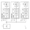
図1に本実施形態の検出装置30X、30Y、30Z等の構成例を示す。物理量測定装置20X、20Y、20Z(センサー)の各々は、対応する各検出装置30X、30Y、30Zと、対応する各物理量トランスデューサー100X、100Y、100Zを含む。検出システム150は、外部デバイス8と、検出装置30X、30Y、30Z(物理量測定装置20X、20Y、20Z)を含む。外部デバイス8は検出装置30X、30Y、30Zに対してバスBS(シリアルバス)を介して通信接続されている。
1. 1. Detection device FIG. 1 shows a configuration example of the
なお検出装置30X、30Y、30Z、物理量測定装置20X、20Y、20Z、検出システム150の構成は図1の構成に限定されず、その構成要素の一部を省略したり、他の構成要素を追加するなどの種々の変形実施が可能である。例えば図1では、3つの検出装置30X、30Y、30Z(3つの物理量測定装置20X、20Y、20Z)を設けているが、これらは2つあってもよいし、4つ以上であってもよい。また、以下では検出装置30X、30Y、30Zのうちの検出装置30Xを主に例にとり、その構成及び動作を説明するが、検出装置30Y、30Zの構成及び動作も同様である。例えば以下では、検出装置30Xを自身の検出装置とし、検出装置30Y、30Zを少なくとも一つの他の検出装置であるとして説明を行う。なお、少なくとも一つの他の検出装置は1つであってもよいし、3つ以上であってもよい。
The configurations of the
図1に示すように検出装置30Xは、インターフェース40X、処理回路50X、検出回路60Xを含む。
As shown in FIG. 1, the
検出回路60X(60Y、60Z)は、物理量トランスデューサー100X(100Y、100Z)からの信号に基づいて検出処理を行い、検出データを出力する。検出回路60Xは、物理量トランスデューサー100Xに信号線を介して接続されている。信号線は例えば検出信号の信号線や駆動信号の信号線などである。例えば検出回路60Xは物理量トランスデューサー100Xからの電圧信号又は電流信号等に基づいて、信号の増幅処理、検波処理、フィルター処理、又はD/A変換処理などの検出処理を行って、物理量トランスデューサー100Xで検出される物理量に対応する検出データを求め、処理回路50Xに出力する。
The
処理回路50X(50Y、50Z)は、検出回路60Xからの検出データに基づいて各種の処理を行う。処理回路50Xは、例えば検出データに対してオフセット補正(ゼロ点補正)又は感度補正等の補正処理や、フィルター処理などの各種の信号処理を行ってもよい。そして処理回路50Xにより検出回路60Xから取り込まれた検出データが、インターフェース40X、バスBSを介して外部デバイス8に送信される。
The
ここで物理量トランスデューサー100X、100Y、100Zは、物理量を検出するための素子やデバイスである。物理量トランスデューサー100X、100Y、100Zは例えば互いに異なる物理量を検出する。物理量は、例えば角速度、角加速度、速度、加速度、距離、圧力、音圧、磁気量又は時間等である。例えば物理量トランスデューサー100X、100Y、100Zは、各々、第1軸、第2軸、第3軸についての物理量を検出してもよい。第1軸、第2軸、第3軸についての物理量とは、例えば第1軸、第2軸、第3軸回りでの角速度又は角加速度、或いは第1軸、第2軸、第3軸方向での速度又は加速度などである。第1軸、第2軸、第3軸は一例としてはX軸、Y軸、Z軸である。なお第1軸、第2軸、第3軸のうちの2軸の物理量だけを検出するものであってもよい。
Here, the
インターフェース40X(40Y、40Z)は、外部デバイス8と通信接続され、外部デバイス8に対して検出データを出力する。例えばインターフェース40X(インターフェース回路、インターフェース部)はバスBSを介して外部デバイス8に接続され、所与の通信プロトコルにしたがって、検出データの転送処理を行う。インターフェース40Xは例えば物理層の回路を少なくても含むものであればよい。例えばインターフェース40Xは、信号を出力又は入力するためのバッファー回路や、シリアル/パラレル変換回路や、或いはパラレル/シリアル変換回路などを含むことができる。
The
バスBSは、例えばSPI又はI2Cなどのシリアル通信規格のバスである。バスBSは、例えばデータ信号線(シリアルデータ信号線)を含む。データ信号線は、送信用と受信用の2本の信号線であってもよいし、送信及び受信に兼用の信号線であってもよい。またバスBSはクロック信号線を含んでもよい。或いはチップセレクト信号線を含んでもよい。外部デバイス8は例えば後述するホストデバイス10であるが、これには限定されない。例えば外部デバイス8はホスト(マスター)の役割のデバイス以外のデバイスであってもよい。
The bus BS is a bus of a serial communication standard such as SPI or I2C. The bus BS includes, for example, a data signal line (serial data signal line). The data signal line may be two signal lines for transmission and reception, or may be a signal line for both transmission and reception. Further, the bus BS may include a clock signal line. Alternatively, a chip select signal line may be included. The
そして本実施形態では、処理回路50X(50Y、50Z)は、少なくとも一つの他の検出装置30Y、30Zと自身の検出装置30Xとに共通の共通取り込みタイミングで取り込まれた検出回路60X(60Y、60Z)からの検出データを、自身の検出装置30Xのデータ送信順番においてインターフェース40X(40Y、40Z)に出力させる。例えば処理回路50Xは、外部デバイス8に通信接続される複数の検出装置30X、30Y、30Zの共通取り込みタイミングでの検出データを取り込む。そしてインターフェース40Xは、共通取り込みタイミングで取り込まれた検出データを、自身のデータ送信順番において外部デバイス8に出力する。インターフェース40Y、40Zも、共通取り込みタイミングで取り込まれた検出データを、自身のデータ送信順番においてバスBSを介して外部デバイス8に出力する。
Then, in the present embodiment, the
例えば処理回路50Xは、少なくとも一つの他の検出装置30Y、30Zと自身の検出装置30Xを共通宛先とする共通宛先コマンドを外部デバイス8から受信した際に、共通取り込みタイミングで取り込まれた検出データを、自身の検出装置30Xのデータ送信順番においてインターフェース40Xに出力させる。例えばインターフェース40Xは、バスBSを介して外部デバイス8に通信接続される複数の検出装置30X、30Y、30Zを共通宛先とする共通宛先コマンドを、外部デバイス8から受信する。処理回路50Xは、このような検出装置30X、30Y、30Zを共通宛先とする共通宛先コマンドを受信したと判断された場合に、共通取り込みタイミングでの検出データを取り込む。そしてインターフェース40Xは、共通取り込みタイミングで取り込まれた検出データを、自身のデータ送信順番においてバスBSを介して外部デバイス8に出力する。
For example, when the
ここで共通取り込みタイミングは、検出装置30X、30Y、30Zを共通宛先とする共通宛先コマンドの受け付けタイミングの後のタイミングであって、少なくとも一つの他の検出装置30Y、30Z及び自身の検出装置30Xの検出データの出力期間の前のタイミングである。即ち、当該共通宛先コマンドを受け付けた後であって、検出装置30X、30Y、30Zが検出データを出力する出力期間の前のタイミングである共通取り込みタイミングにおいて、処理回路50X、50Y、50Zは検出データを取り込む。そして、インターフェース40X、40Y、40Zの各々は、共通取り込みタイミングで取り込まれた検出データを、自身のデータ送信順番において出力する。ここで処理回路50X、50Y、50Zは、後述の図10に示すようにコマンドデコーダー52を含み、共通宛先コマンドの受け付けタイミングは、コマンドデコーダー52が、当該共通宛先コマンドを受け付けたと判断したタイミングである。
Here the common
また、この共通宛先コマンドは、後述の図6、図7で説明するように、少なくとも一つの他の検出装置30Y、30Zと自身の検出装置30Xとを共通宛先とする共通アドレス(例えば00)を指定して外部デバイス8が発行するリードコマンドなどである。但し、共通宛先コマンドは、このようなリードコマンドには限定されず、例えば外部デバイス8が、検出装置30X、30Y、30Zに対して、共通取り込みタイミングで検出データを取り込むことを指示するような特定のコマンド(リードコマンドとは別のコマンド)であってもよい。
Further, this common destination command sets a common address (for example, 00) having at least one
図2は本実施形態の比較例の手法を説明する動作説明図である。検出装置30X、30Y、30Zは、外部デバイス8からバスBSを介して、検出装置30X、30Y、30Zを共通宛先とする共通宛先コマンドを受信する。検出装置30X、30Y、30Zは、この共通宛先コマンドを受信すると、自身のデータ送信順番において、検出データDX、DY、DZを出力する。図2では、検出装置30Xが検出データDXを出力し、次に検出装置30Yが検出データDYを出力し、次に検出装置30Zが検出データDZを出力している。なお、ここでは共通宛先コマンドは8ビットのコマンドになっており、検出データDX、DY、DZは24ビットのデータになっている。但し、共通宛先コマンド、検出データのビット数はこれに限定されない。
FIG. 2 is an operation explanatory diagram illustrating the method of the comparative example of the present embodiment. The
検出装置30X、30Y、30Zは、図2に示すようなタイミングで検出データの内部更新を行っている。例えば図2に示す内部更新タイミングで、検出装置30X、30Y、30Zの検出回路60X、60Y、60Zが検出データの検出処理を行って、検出データを処理回路50X、50Y、50Zに出力する。そして検出装置30Xは、図2のD1に示す取り込みタイミングで取り込まれた検出データDXを、自身のデータ送信順番においてバスBSに出力する。検出装置30Yは、D2に示す取り込みタイミングで取り込まれた検出データDYを、自身のデータ送信順番においてバスBSに出力する。検出装置30Zは、D3に示す取り込みタイミングで取り込まれた検出データDZを、自身のデータ送信順番においてバスBSに出力する。これらのD1、D2、D3の取り込みタイミングは、バスBSにおける検出データDX、DY、DZの出力期間の前(直前)のタイミングである。即ち検出装置30X、30Y、30Zは、その出力期間の直前に取り込まれた検出データDX、DY、DZをバスBSに出力する。
The
ここで検出装置30X、30Y、30Zの各々は、その内部に設けられた後述の図9のクロック信号生成回路72からのクロック信号に基づき動作している。このクロック信号生成回路72は、後述の図9の振動子110を用いてクロック信号を生成したり、或いはCR発振回路等の発振回路を用いてクロック信号を生成する。このため検出装置30X、30Y、30Zで使用されるクロック信号は、互いに非同期となっており、図2に示すように検出データの内部更新タイミングも互いに非同期になっている。
Here, each of the
例えば複数の検出装置30X、30Y、30Zからの検出データDX、DY、DZに基づいて、検出対象物の姿勢情報、移動距離情報等の情報を適正に求めるためには、各検出データDX、DY、DZの同期がとれているか、或いは検出データDX、DY、DZを取得した時間が明確になっていることが望まれる。
For example, in order to appropriately obtain information such as attitude information and movement distance information of a detection target object based on the detection data DX, DY, DZ from a plurality of
しかしながら、図2の比較例の手法では、D1、D2、D3に示すように、検出データDX、DY、DZの取り込みタイミングが互いに異なっており、同期が取れていない。例えば検出装置30Zの検出データDZの取り込みタイミング(D3)は、検出装置30Xの検出データDXの取り込みタイミング(D1)に比べて、48ビット分だけ遅れたタイミングになっている。また、例えば外部デバイス8からの読み出し用のクロック信号(後述の図6のSCLK)に基づき、検出データDX、DY、DZの読み出しが行われる場合に、この読み出し用のクロック信号の周波数や出力タイミングは、外部デバイス8の処理に依存してしまう。このため、図2のD1、D2、D3がどのようなタイミングになるのかを、明確に特定することができないという問題がある。
However, in the method of the comparative example of FIG. 2, as shown in D1, D2, and D3, the capture timings of the detected data DX, DY, and DZ are different from each other, and they are not synchronized. For example, the capture timing (D3) of the detection data DZ of the
このように図2の比較例の手法では、検出データDX、DY、DZの取り込みタイミングが、異なったタイミング(D1、D2、D3)になってしまい、同期が取れておらず、どのようなタイミングなのかを明確に特定できない。従って、検出データDX、DY、DZを用いて、例えば検出対象物の姿勢情報、移動距離情報等の情報を求める場合に、適正な情報を取得できないという問題がある。例えば検出データDX、DY、DZがX軸、Y軸、Z軸回りの角速度データである場合に、X軸、Y軸、Z軸回りの角速度データである検出データDX、DY、DZは、図2の比較例の手法では異なったタイミングで取得されたデータになってしまう。従って、これらの検出データDX、DY、DZに基づき特定される検出対象物の姿勢情報は、不正確な情報になってしまうおそれがある。同様に、検出データDX、DY、DZがX軸、Y軸、Z軸方向の加速度データである場合に、これらの検出データDX、DY、DZに基づき特定される検出対象物の移動距離情報は、不正確な情報になってしまうおそれがある。また例えば後述の図5のように、同じ座標軸についての角速度データ又は加速度データを複数の検出装置を用いて検出して、その平均値を求める場合がある。この場合にも、図2の比較例の手法では、平均値を求める際に使用する検出データの取り込みタイミングが、異なったタイミングになってしまうため、適正な平均値を求めることができないという問題がある。 As described above, in the method of the comparative example of FIG. 2, the capture timings of the detected data DX, DY, and DZ are different timings (D1, D2, D3), and the synchronization is not achieved. I can't clearly identify it. Therefore, when the detection data DX, DY, and DZ are used to obtain information such as posture information and movement distance information of the detection target object, there is a problem that appropriate information cannot be obtained. For example, when the detection data DX, DY, and DZ are angular velocity data around the X-axis, Y-axis, and Z-axis, the detection data DX, DY, and DZ, which are the angular velocity data around the X-axis, Y-axis, and Z-axis, are shown in the figure. In the method of the comparative example of 2, the data is acquired at different timings. Therefore, the posture information of the detection target object specified based on these detection data DX, DY, and DZ may become inaccurate information. Similarly, when the detection data DX, DY, and DZ are acceleration data in the X-axis, Y-axis, and Z-axis directions, the movement distance information of the detection target object specified based on these detection data DX, DY, and DZ is , There is a risk of inaccurate information. Further, for example, as shown in FIG. 5 described later, there is a case where angular velocity data or acceleration data for the same coordinate axis is detected by using a plurality of detection devices and the average value thereof is obtained. In this case as well, the method of the comparative example of FIG. 2 has a problem that an appropriate average value cannot be obtained because the acquisition timing of the detection data used when obtaining the average value is different. is there.
このような問題を解決するために本実施形態では、複数の検出装置30X、30Y、30Zに共通の共通取り込みタイミングで取り込まれた検出データを、自身のデータ送信順番において出力する手法を採用している。
In order to solve such a problem, in the present embodiment, a method of outputting the detection data captured at the common capture timing common to the plurality of
例えば図3では、図2と同様に、検出装置30X、30Y、30Zは、外部デバイス8からバスBSを介して、検出装置30X、30Y、30Zを共通宛先とする共通宛先コマンドを受信する。検出装置30X、30Y、30Zは、共通宛先コマンドを受信すると、自身のデータ送信順番において、検出データDX、DY、DZを出力する。また検出装置30X、30Y、30Zは、図3に示すようなタイミングで検出データの内部更新を行っている。
For example, in FIG. 3, similarly to FIG. 2, the
そして本実施形態では、検出装置30X、30Y、30Zの処理回路50X、50Y、50Zは、E1、E2、E3に示すような共通取り込みタイミングで、検出回路60X、60Y、60Zからの検出データDX、DY、DZを取り込む。そして検出装置30X、30Y、30Zは、E1、E2、E3に示す共通取り込みタイミングで取り込まれた検出データDX、DY、DZを、自身のデータ送信順番で出力する。具体的には、まず検出装置30Xが、E1に示す共通取り込みタイミングで取り込まれた検出データDXを、バスBSに出力する。次に検出装置30Yが、E2に示す共通取り込みタイミングで取り込まれた検出データDYを、バスBSに出力する。次に検出装置30Zが、E3に示す共通取り込みタイミングで取り込まれた検出データDZを、バスBSに出力する。
Then, in the present embodiment, the
このように本実施形態では、共通取り込みタイミングで取り込まれた検出データDX、DY、DZが、自身のデータ送信順番において順次に出力される。従って、検出装置30X、30Y、30Zの検出データDX、DY、DZがどのタイミングで更新されたデータかを明確に把握することが可能になる。例えば検出装置30X、30Y、30Zの検出データDX、DY、DZを同時に確定することが可能になる。従って、検出データDX、DY、DZを用いて、例えば検出対象物の姿勢情報、移動距離情報等の情報を求める場合に、適正な情報を取得できるようになる。例えば検出データDX、DY、DZがX軸、Y軸、Z軸回りの角速度データである場合に、図3のE1、E2、E3に示すような共通取り込みタイミングで取り込まれた検出データDX、DY、DZに基づいて、検出対象物の姿勢情報を求めることができるため、適正な姿勢情報の取得が可能になる。また検出データDX、DY、DZがX軸、Y軸、Z軸方向の加速度データである場合に、共通取り込みタイミングで取り込まれた検出データDX、DY、DZに基づいて、検出対象物の移動距離情報を求めることができるため、適正な移動距離情報の取得が可能になる。また後述の図5のように、同じ座標軸についての角速度データ又は加速度データを複数の検出装置を用いて検出して平均値を求める場合に、共通取り込みタイミングで取り込まれた検出データDX、DY、DZに基づいて、平均値(統計値)を求めることができるため、適正な平均値を求めることが可能になる。
As described above, in the present embodiment, the detection data DX, DY, and DZ captured at the common capture timing are sequentially output in the order of own data transmission. Therefore, it is possible to clearly grasp at what timing the detection data DX, DY, and DZ of the
なお、図3のE1、E2、E3では、共通取り込みタイミングは完全には一致したタイミングになっていない。例えば検出装置30X、30Y、30Zは、内蔵するクロック信号生成回路72より生成されたクロック信号に基づき動作する。このため、検出データDX、DY、DZの内部更新タイミングは非同期であり、E1、E2、E3に示す共通取り込みタイミングも非同期になり、これらのタイミングは一致したタイミングにならない。即ち、これらの共通取り込みタイミングは、共通取り込み期間内のタイミングであればよい。例えば共通取り込みタイミングは、クロック信号の1クロックサイクル又は数クロックサイクルだけずれたタイミングであってもよく、1クロックサイクル又は数クロックサイクルの期間内のタイミングであればよい。例えば図2の比較例の手法では、取り込みタイミングが、各検出データの出力期間の長さ以上、ずれたタイミングとなっているが、共通取り込みタイミングのずれは、各検出データの出力期間の長さよりも短いずれである。
In E1, E2, and E3 of FIG. 3, the common capture timings do not completely match. For example, the
また本実施形態では検出装置30X、30Y、30Zを共通宛先とする共通宛先コマンドを外部デバイス8から受信した際に、共通取り込みタイミングで取り込まれた検出データDX、DY、DZを、自身のデータ送信順番において出力している。このようにすれば、外部デバイス8が検出装置30X、30Y、30Zに対して、例えば共通アドレスを指定したリードコマンドなどのコマンドを発行することで、検出データの取り込みタイミングが特定されて、検出装置30X、30Y、30Zの検出データDX、DY、DZを同時に確定することが可能になる。従って、例えば検出装置30X、30Y、30Zが、共通宛先コマンドを受信してから、所与のクロックサイクル数が経過したタイミングで検出データDX、DY、DZを取り込むことで、図3のE1、E2、E3に示すような共通取り込みタイミングでの検出データDX、DY、DZの取り込み処理が可能になる。従って、簡素な処理シーケンスでの検出データDX、DY、DZの取り込み処理が可能になる。
Further, in the present embodiment, when a common destination command with the
なお、図3では、検出装置30X、30Y、30Zを共通宛先とする共通宛先コマンドを用いて、共通取り込みタイミングを特定しているが、本実施形態はこれに限定されない。例えば共通取り込みタイミングの特定を、端子設定により行ってもよい。例えば検出装置30X、30Y、30Zに対して、共通取り込みタイミングの設定用の端子を設ける。そして外部デバイス8が、この設定用の端子に対してタイミング特定用の信号を出力することで、検出装置30X、30Y、30Zが共通取り込みタイミングを特定するようにしてもよい。また例えば検出装置30Xが共通取り込みタイミング信号を出力し、検出装置30Y、30Zが、その共通取り込みタイミング信号を受信して、共通取り込みタイミングを特定するようにしてもよい。また共通取り込みタイミングは、処理回路50Xのデジタルシーケンス処理において特定されるタイミングとすることができる。例えば、共通取り込みタイミングでの検出データを取り込むように、処理回路50Xのデジタル回路が構成(設計)されている。例えば処理回路50Xの動作クロック信号のクロックサイクル数により共通取り込みタイミングが設定されている。そして例えば動作クロック信号の何番目のクロックサイクルで検出データを取り込むかを設定しておくことで、共通取り込みタイミングでの検出データの取り込み処理が実現される。
In FIG. 3, the common capture timing is specified by using the common destination command with the
図4に本実施形態の第2の構成例を示す。図1の構成例では検出装置が互いに異なる物理量を検出しているが、図4の第2の構成例では検出装置が同じ物理量を検出している。 FIG. 4 shows a second configuration example of the present embodiment. In the configuration example of FIG. 1, the detection devices detect different physical quantities, but in the second configuration example of FIG. 4, the detection devices detect the same physical quantity.
即ち、図1では、少なくとも一つの他の検出装置である検出装置30Y、30Zと、自身の検出装置30Xとは、互いに異なる物理量についての検出データを検出し、共通取り込みタイミングにおいて、互いに異なる物理量についての検出データを取り込んでいる。一例としては、検出装置30Yは、Y軸回りの角速度又はY軸方向での加速度を検出し、検出装置30Zは、Z軸回りの角速度又はZ軸方向での加速度を検出する。これに対して検出装置30Xは、X軸回りの角速度又はX軸方向での加速度を検出しており、検出装置30Y、30Zとは、互いに異なる物理量を検出している。このような互いに異なる物理量によって、例えば検出対象物の姿勢情報や移動距離情報等の情報が求められる場合には、互いに異なる物理量についての検出データが、共通取り込みタイミングで取り込まれることで、当該情報を適正に求めることが可能になる。
That is, in FIG. 1, at least one other detection device, the
これに対して図4では、少なくとも一つの他の検出装置である検出装置30X2と、自身の検出装置30X1とは、同じ物理量についての検出データを検出し、共通取り込みタイミングにおいて、同じ物理量についての検出データを取り込む。また少なくとも一つの他の検出装置である検出装置30Y2と、検出装置30Y1とは、同じ物理量についての検出データを検出し、共通取り込みタイミングにおいて、同じ物理量についての検出データを取り込む。検出装置30Z2と検出装置30Z1についても同様である。このように同じ物理量が検出される場合に、当該同じ物理量に基づく統計処理などの演算処理が行われる場合に、より適切な演算処理の実現が可能になる。例えば同じ物理量についての平均値を求める演算処理が行われる場合には、より適正な平均値の演算処理を実現できる。 On the other hand, in FIG. 4, at least one other detection device, the detection device 30X2, and its own detection device 30X1 detect detection data for the same physical quantity, and detect the same physical quantity at the common capture timing. Capture data. Further, the detection device 30Y2 and the detection device 30Y1 which are at least one other detection device detect the detection data for the same physical quantity, and capture the detection data for the same physical quantity at the common capture timing. The same applies to the detection device 30Z2 and the detection device 30Z1. When the same physical quantity is detected in this way, more appropriate arithmetic processing can be realized when arithmetic processing such as statistical processing based on the same physical quantity is performed. For example, when an arithmetic process for obtaining an average value for the same physical quantity is performed, a more appropriate arithmetic process for the average value can be realized.
ここで同じ物理量についての検出データは、同じ軸回りでの角速度又は同じ軸方向での加速度についての検出データなどである。例えば検出装置30X1と検出装置30X2は、例えば第1軸回りでの角速度又は第1軸方向での加速度を検出しており、同じ物理量を検出している。検出装置30Y1と検出装置30Y2は、例えば第2軸回りでの角速度又は第2軸方向での加速度を検出しており、同じ物理量を検出している。検出装置30Z1と検出装置30Z2は、例えば第3軸回りでの角速度又は第3軸方向での加速度を検出しており、同じ物理量を検出している。このようにすれば、例えば角速度又は加速度についての統計処理などの演算処理が行われる場合に、より適切な演算処理の実現が可能になる。例えば角速度又は加速度の平均値を求める演算処理が行われる場合には、より適正な平均値を求めることができる。例えば外部デバイス8が、角速度の積分処理(積算処理)を行って、角度を求めたり、加速度の積分処理を行って、速度や距離を求める場合に、より高い精度で、角度、速度又は距離等の情報を求めることが可能になる。
Here, the detection data for the same physical quantity is the detection data for the angular velocity around the same axis or the acceleration in the same axial direction. For example, the detection device 30X1 and the detection device 30X2 detect, for example, the angular velocity around the first axis or the acceleration in the first axis direction, and detect the same physical quantity. The detection device 30Y1 and the detection device 30Y2 detect, for example, the angular velocity around the second axis or the acceleration in the second axis direction, and detect the same physical quantity. The detection device 30Z1 and the detection device 30Z2 detect, for example, the angular velocity around the third axis or the acceleration in the third axis direction, and detect the same physical quantity. In this way, when arithmetic processing such as statistical processing for angular velocity or acceleration is performed, more appropriate arithmetic processing can be realized. For example, when the arithmetic processing for obtaining the average value of the angular velocity or the acceleration is performed, a more appropriate average value can be obtained. For example, when the
図5は、図4の第2の構成例の動作説明図である。図5の検出データDX1、DX2は、図4の検出装置30X1、30X2の検出データである。例えば検出データDX1、DX2はX軸回りの角速度又はX軸方向の加速度である。また検出データDY1、DY2は、検出装置30Y1、30Y2の検出データであり、検出データDZ1、DZ2は、検出装置30Z1、30Z2の検出データである。例えば検出データDY1、DY2はY軸回りの角速度又はY軸方向の加速度であり、検出データDZ1、DZ2はZ軸回りの角速度又はZ軸方向の加速度である。 FIG. 5 is an operation explanatory view of the second configuration example of FIG. The detection data DX1 and DX2 in FIG. 5 are the detection data of the detection devices 30X1 and 30X2 in FIG. For example, the detection data DX1 and DX2 are angular velocities around the X-axis or accelerations in the X-axis direction. Further, the detection data DY1 and DY2 are the detection data of the detection devices 30Y1 and 30Y2, and the detection data DZ1 and DZ2 are the detection data of the detection devices 30Z1 and 30Z2. For example, the detection data DY1 and DY2 are the angular velocity around the Y-axis or the acceleration in the Y-axis direction, and the detection data DZ1 and DZ2 are the angular velocity around the Z-axis or the acceleration in the Z-axis direction.
そして検出データDX1、DX2は、図5のF1に示す共通取り込みタイミングで取り込まれたデータである。即ち、F1に示すタイミングは、検出装置30X1、30X2の共通取り込みタイミングであり、検出装置30X1、30X2は、このF1のタイミングで検出データDX1、DX2を取り込む。そして例えば外部デバイス8により、検出データDX1とDX2の平均値を求める演算処理が行われる。
The detection data DX1 and DX2 are data captured at the common capture timing shown in F1 of FIG. That is, the timing shown in F1 is the common capture timing of the detection devices 30X1 and 30X2, and the detection devices 30X1 and 30X2 capture the detection data DX1 and DX2 at the timing of F1. Then, for example, the
また検出データDY1、DY2は、検出装置30Y1、30Y2により、図5のF2に示す共通取り込みタイミングで取り込まれたデータである。そして例えば外部デバイス8により、検出データDY1とDY2の平均値を求める演算処理が行われる。同様に検出データDZ1、DZ2は、検出装置30Z1、30Z2により、F3に示す共通取り込みタイミングで取り込まれる。そして例えば外部デバイス8により、検出データDZ1とDZ2の平均値を求める演算処理が行われる。
Further, the detection data DY1 and DY2 are data captured by the detection devices 30Y1 and 30Y2 at the common capture timing shown in F2 of FIG. Then, for example, the
このように検出データの平均値を求める処理を行うことで、検出データに対応する物理量を、高い精度で検出できるようになる。例えば検出データの平均化処理を行うことで、ノイズ成分を低減できるようになり、よりS/N比の高い物理量の検出値を取得できるようになる。なお、図4、図5では、角速度又は加速度等の同じ物理量を、2つの検出装置で検出して平均化処理を行う場合を示したが、同じ物理量を検出する検出装置は3つ以上であってもよい。このように同じ物理量を検出する検出装置の数を増やすことで、物理量の検出精度を更に高めることが可能になる。 By performing the process of obtaining the average value of the detected data in this way, the physical quantity corresponding to the detected data can be detected with high accuracy. For example, by performing the detection data averaging process, the noise component can be reduced, and the detected value of the physical quantity having a higher S / N ratio can be obtained. In addition, in FIGS. 4 and 5, the case where the same physical quantity such as angular velocity or acceleration is detected by two detection devices and the averaging process is performed is shown, but there are three or more detection devices that detect the same physical quantity. You may. By increasing the number of detection devices that detect the same physical quantity in this way, it is possible to further improve the detection accuracy of the physical quantity.
2.詳細な構成例
図6に本実施形態の検出装置30X、30Y、30Z、物理量測定装置20X、20Y、20Z、検出システム150の詳細な構成例を示す。図6では、マスターとなるホストデバイス10(広義には外部デバイス)と、スレーブとなる検出装置30X、30Y、30ZがSPI(Serial Peripheral Interface)により通信接続されている。XCSはチップセレクト信号、SCLKはクロック信号、SDIはデータ入力信号、SDOはデータ出力信号である。ホストデバイス10は、各種のプロセッサー(CPU、MPU)やASICのハードウェア回路等により実現できる。例えばホストデバイス10(ホストコントローラー)としてはマイコンを用いることができる。物理量測定装置20X、20Y、20Zの各々は、対応する検出装置30X、30Y、30Zと、対応する物理量トランスデューサー100X、100Y、100Zを有しており、X軸用ジャイロセンサー、Y軸用ジャイロセンサー、Z軸用ジャイロセンサーである。これらのジャイロセンサーをSPIにより通信接続することで、多軸ジャイロセンサーが実現される。なお図6では3つの物理量測定装置(センサー)20X、20Y、20Zが設けられているが、物理量測定装置の数は2個でもよいし、4個以上であってもよい。また物理量測定装置20X、20Y、20Zはジャイロセンサー以外のセンサーであってもよく、例えば加速度センサーなどであってもよい。この場合には物理量測定装置20X、20Y、20Zは、X軸用加速度センサー、Y軸用加速度センサー、Z軸用加速度センサーとなる。
2. Detailed Configuration Example FIG. 6 shows a detailed configuration example of the
なお、以下では、物理量トランスデューサー100X、100Y、100Zが圧電型の振動子(振動ジャイロ)であり、物理量測定装置20X、20Y、20Zがジャイロセンサーである場合を主に例にとり説明するが、本実施形態はこれに限定されない。例えばシリコン基板などから形成された静電容量検出方式の振動子(振動ジャイロ)や、角速度情報と等価な物理量や角速度情報以外の物理量を検出するセンサー(加速度センサー)などの種々の物理量トランスデューサーに本実施形態は適用可能である。
In the following, the case where the
検出装置30X(30Y、30Z)は、インターフェース40X(40Y、40Z)、処理回路50X(50Y、50Z)、検出回路60X(60Y、60Z)、記憶部70X(70Y、70Z)を含む。
The
検出回路60Xは、物理量トランスデューサー100Xからの信号に基づいて所望信号の検出処理を行う。そして検出処理により得られたアナログの検出信号のA/D変換を行って、デジタルの検出データを出力する。物理量測定装置20X、20Y、20Zがジャイロセンサーである場合には、物理量トランスデューサー100X、100Y、100Zは振動子であり、検出回路60Xは、例えばX軸回り(広義には所定軸回り)の角速度を検出する回路となる。そして検出回路60Xの検出データは、X軸回りでの角速度データになる。また検出回路60Y、60Zは、各々、Y軸回り、Z軸回りの角速度を検出する回路となり、検出回路60Y、60Zの検出データは、各々、Y軸回り、Z軸回りでの角速度データになる。またこの場合には、振動子を駆動する駆動回路が更に設けられることになる。
The
インターフェース40Xは、マスターであるホストデバイス10と通信を行う。例えばインターフェース40Xは、クロック信号SCLKとデータ入力信号SDIとデータ出力信号SDOを用いてホストデバイス10と通信を行う。
The
具体的には図6では、クロック信号SCLKとデータ入力信号SDIとデータ出力信号SDOが、検出装置30X、30Y、30Zで共用されており、ホストデバイス10のSCLK、SDI、SDOの信号線が検出装置30X、30Y、30Zに共通接続されている。そしてインターフェース40Xは、クロック信号SCLKとデータ入力信号SDIとデータ出力信号SDOを用いて、ホストデバイス10と例えばSPIの通信方式で通信を行う。
Specifically, in FIG. 6, the clock signal SCLK, the data input signal SDI, and the data output signal SDO are shared by the
また図6では、チップセレクト信号XCSについても、検出装置30X、30Y、30Zで共用されており、ホストデバイス10のXCSの信号線が検出装置30X、30Y、30Zに共通接続されている。
Further, in FIG. 6, the chip select signal XCS is also shared by the
記憶部70Xは各種の情報を記憶する。記憶部70X(70Y、70Z)はEPROM(Erasable Programmable ROM)、OTP(One Time Programmable ROM)などの不揮発性メモリーなどにより実現できる。なお不揮発性メモリー以外の半導体メモリーにより記憶部70X(70Y、70Z)を実現してもよい。
The
記憶部70Xは、自身の検出装置30Xのデータ送信順番の情報を記憶する。例えばスレーブとしてホストデバイス10に通信接続される複数の検出装置30X、30Y、30Zの中での自身の検出装置30Xのデータ送信順番の情報を記憶する。同様に、検出装置30Yの記憶部70Yは、自身の検出装置30Yのデータ送信順番の情報を記憶し、検出装置30Zの記憶部70Zは、自身の検出装置30Zのデータ送信順番の情報を記憶する。なおデータ送信順番の情報は、データ送信順番そのものであってもよいし、データ送信順番を特定するための情報であってもよい。
The
そしてホストデバイス10が、ホストデバイス10に通信接続される検出装置30X、30Y、30Z(複数の検出装置)を共通宛先とする共通アドレス(例えば00)を指定してリードコマンドを発行したとする。この場合には、インターフェース40Xは、記憶部70Xに記憶される自身のデータ送信順番において、ホストデバイス10に対して検出データを送信する。
Then, it is assumed that the
一方、ホストデバイス10が、個別アドレス(スレーブアドレス)を指定してリードコマンドを発行したとする。この場合には、インターフェース40Xは、ホストデバイス10が指定した個別アドレスが、自身の検出装置30X(物理量測定装置20X)の個別アドレス(例えば01)に合致した場合に、ホストデバイス10に対して検出データを送信する。
On the other hand, it is assumed that the
例えば図6に示すように、記憶部70X、70Y、70Zは、送信順番を指定するkの情報を記憶しており、検出装置30X、30Y、30Zの送信順番は、各々、k=1、k=2、k=3に設定されている。また共通アドレスが(00)であり、検出装置30X、30Y、30Zの個別アドレスが、各々、(01)、(10)、(11)であったとする。
For example, as shown in FIG. 6, the
この場合に、ホストデバイス10が、共通アドレス(00)を指定してリードコマンドを発行すると、検出装置30Xのインターフェース40Xは、第1の送信順番(k=1)で検出データを送信する。また検出装置30Yのインターフェース40Yは、第2の送信順番(k=2)で検出データを送信し、検出装置30Zのインターフェース40Zは、第3の送信順番(k=3)で検出データを送信する。
In this case, when the
一方、ホストデバイス10が、個別アドレス(01)を指定してリードコマンドを発行すると、検出装置30Xのインターフェース40Xが検出データを送信する。同様に、個別アドレス(10)、(11)が指定された場合には、各々、インターフェース40Y、40Zが検出データを送信する。
On the other hand, when the
また記憶部70Xは、ホストデバイス10に通信接続される検出装置の接続個数の情報を記憶する。例えば図6では、接続個数はn=3であるため、n=3の情報を記憶する。同様に記憶部70Y、70Zも接続個数の情報を記憶する。なお接続個数の情報は、接続個数そのものであってもよいし、接続個数を特定するための情報であってもよい。
Further, the
また検出装置の接続個数をnとし、データ送信順番をk(k、nは、1≦k≦nとなる自然数)としたとする。この場合にインターフェース40Xは、データ送信順番である第1の順番(第kの順番。k=1)においてホストデバイス10に対して検出データを送信した後、第4の順番(第n+kの順番)において、ホストデバイス10に対して検出データを送信する。同様に第7の順番(第2n+kの順番)、第10の順番(第3n+kの順番)というように検出データを送信する。インターフェース40Y、40Zの動作も同様である。
Further, it is assumed that the number of connected detection devices is n and the data transmission order is k (k and n are natural numbers such that 1 ≦ k ≦ n). In this case, the
また記憶部70X、70Y、70Zは、検出データの送信データビット数mの情報を記憶する。そしてユーザーが任意に送信データビット数を設定できるようになっている。そしてインターフェース40X、40Y、40Zは、自身のデータ送信順番において、ホストデバイス10に対してその送信データビット数mの検出データを送信する。
Further, the
前述したように本実施形態では、検出装置30X、30Y、30Zを共通宛先とする共通宛先コマンドを、外部デバイス8であるホストデバイス10から受信した際に、インターフェース40Xが、共通取り込みタイミングで取り込まれた検出データを自身の検データ送信順番において出力する。そして図6では、当該共通宛先コマンドは、少なくとも一つの他の検出装置30Y、30Zと自身の検出装置30Xとを共通宛先とする共通アドレスを指定してホストデバイス10(外部デバイス)が発行するリードコマンドとなっている。
As described above, in the present embodiment, when the common destination command with the
ここで、共通アドレス(グローバルアドレス)は、ホストに通信接続される複数のスレーブを共通宛先とするアドレスである。例えば複数のスレーブの全てを宛先とするアドレスである。従って、この共通アドレスがホストにより指定された場合には、全てのスレーブが動作する。一方、ホストにより個別アドレスが指定された場合には、スレーブは、ホストが指定した個別アドレスが自身の個別アドレスと合致した場合にのみ、通信を行う。なお、スレーブのSDOの端子は、アドレスが合致した場合にのみデータが出力され、アドレスが合致しない場合には、ハイインピーダンス状態に設定される。これにより信号の衝突が回避される。 Here, the common address (global address) is an address having a plurality of slaves communicated and connected to the host as a common destination. For example, it is an address destined for all of a plurality of slaves. Therefore, when this common address is specified by the host, all slaves operate. On the other hand, when the individual address is specified by the host, the slave communicates only when the individual address specified by the host matches its own individual address. The slave SDO terminal outputs data only when the addresses match, and is set to a high impedance state when the addresses do not match. This avoids signal collisions.
図7は本実施形態の詳細な構成例の動作を説明する信号波形例である。図7のデータ入力信号SDIの最初の1ビットのR/Wは、リード/ライトを指示するビットである。R/W=1の場合にはリードが指示され、R/W=0の場合にはライトが指示される。R/Wの次の2ビットのA[1:0]は、アドレスを指定するものである。共通アドレスを指定する場合にはA[1:0]=00となる。検出装置30X、30Y、30Zの個別アドレスを指定する場合には、各々、A[1:0]=01、10、11となる。A[1:0]の次の4ビットのC[4:0]は、コマンド内容及びレジスターアドレスを指示するものである。
FIG. 7 is a signal waveform example for explaining the operation of the detailed configuration example of the present embodiment. The first 1-bit R / W of the data input signal SDI of FIG. 7 is a bit indicating read / write. When R / W = 1, a read is instructed, and when R / W = 0, a write is instructed. The next 2-bit A [1: 0] of R / W specifies an address. When a common address is specified, A [1: 0] = 00. When the individual addresses of the
図7では、G1に示すようにR/W=1となっており、リードが指示されており、ホストデバイス10がリードコマンドを発行している。またG2に示すようにA[1:0]=00となっており、共通アドレスが指定されている。またG3によってコマンド内容やレジスターアドレスが指示されている。これにより、検出装置30X、30Y、30Zからの検出データの連続読み出しが実行される。即ち、検出装置30X、30Y、30Zからの検出データがデータ出力信号SDOとして順次に出力される。
In FIG. 7, as shown in G1, R / W = 1, the read is instructed, and the
そして図6に示すように、検出装置30X、30Y、30Zのデータ送信順番は、各々、k=1、k=2、k=3に設定されており、送信データビット数はm=8に設定されている。従って、出力期間T1では、データ送信順番がk=1である検出装置30Xから、m=8ビットの検出データが出力される。次の出力期間T2では、データ送信順番がk=2である検出装置30Yから、m=8ビットの検出データが出力される。次の出力期間T3では、データ送信順番がk=3である検出装置30Zから、m=8ビットの検出データが出力される。
As shown in FIG. 6, the data transmission order of the
このように本実施形態の詳細な構成例によれば、ホストデバイスにより共通アドレスが指定されてリードコマンドが発行されると、予め設定されたデータ送信順番で各検出装置が検出データを送信する。また、送信される検出データの送信データビット数も予め設定されたビット数になっている。従って、ホストデバイスは、各検出装置から順次に連続的に送信された検出データをリードして取得できるようになる。即ち、データ送信順番を不揮発性メモリー等の記憶部に記憶しておくことで、各検出装置が何番目に検出データを出力すればよいのかを、予め取り決めしておくことができる。接続個数や送信データビット数を記憶部に記憶しておくことで、何個の検出装置がホストデバイスに接続されているのかや、何ビットの検出データを各検出装置が出力するのかについても、予め取り決めしておくことができる。従って、各検出装置は、その取り決めにしたがって検出データを出力するだけでよいため、その処理や制御を簡素化できる。またホストデバイスも、その取り決めにしたがって、検出装置からの検出データを取り込めばよいため、その処理や制御を簡素化できる。 As described above, according to the detailed configuration example of the present embodiment, when the common address is specified by the host device and the read command is issued, each detection device transmits the detection data in the preset data transmission order. Further, the number of transmission data bits of the detected data to be transmitted is also a preset number of bits. Therefore, the host device can read and acquire the detection data sequentially and continuously transmitted from each detection device. That is, by storing the data transmission order in a storage unit such as a non-volatile memory, it is possible to decide in advance which order each detection device should output the detection data. By storing the number of connections and the number of transmission data bits in the storage unit, it is also possible to determine how many detection devices are connected to the host device and how many bits of detection data each detection device outputs. It can be arranged in advance. Therefore, each detection device only needs to output the detection data according to the agreement, so that the processing and control can be simplified. Further, since the host device may also take in the detection data from the detection device according to the agreement, the processing and control thereof can be simplified.
そして本実施形態では、図7のG4に示す共通取り込みタイミングで取り込まれた検出データが、出力期間T1、T2、T3において検出装置30X、30Y、30Zから出力される。即ち、G4の共通取り込みタイミングで検出回路60Xから取り込まれた検出データが、出力期間T1において、検出装置30Xのインターフェース40Xから出力される。またG4の共通取り込みタイミングで検出回路60Yから取り込まれた検出データが、出力期間T2において、検出装置30Yのインターフェース40Yから出力される。またG4の共通取り込みタイミングで検出回路60Zから取り込まれた検出データが、出力期間T3において、検出装置30Zのインターフェース40Zから出力される。このようにすることで、共通取り込みタイミングでの検出データが検出装置30X、30Y、30Zから出力されるようになる。従って、検出データがどのタイミングで取り込まれたデータなのかが明確になり、これらの検出データにより特定される情報として、より適正な情報を取得できるようになる。
Then, in the present embodiment, the detection data captured at the common capture timing shown in G4 of FIG. 7 is output from the
そして図7に示すように、G4に示す共通取り込みタイミングは、G1、G2、G3に示すコマンド(共通宛先コマンド)の受け付けタイミングの後のタイミングであって、検出装置30X、30Y、30Z(少なくとも一つの他の検出装置と自身の検出装置)の検出データの出力期間T1、T2、T3の前のタイミングとなっている。このコマンド(共通宛先コマンド)の受け付けタイミングは、後述の図10のコマンドデコーダー52がコマンド(共通宛先コマンド)を受け付けたと判断したタイミングである。即ち、検出装置30X、30Y、30Zを共通宛先とする共通アドレス(例えば00)を指定して発行されたリードコマンドを、受け付けたと判断したタイミングである。このようなコマンド(共通宛先コマンド)の受け付けタイミングの後であって、出力期間T1、T2、T3の前のタイミング(G4)において、各検出回路60X、60Y、60Zからの検出データを取り込む。そして各検出装置30X、30Y、30Zは、取り込んだ検出データを、各出力期間T1、T2、T3において出力する。
As shown in FIG. 7, the common capture timing shown in G4 is a timing after the acceptance timing of the command (common destination command) shown in G1, G2, and G3, and is the timing after the
このようにすれば、検出装置30X、30Y、30Zは、より小さなタイムラグで検出データを出力できるようになる。例えば図7では、取り込みタイミングからの遅延時間であるタイムラグは、検出装置30Zの出力期間T3が最も大きくなるが、共通取り込みタイミングをG4に示すタイミングとすることで、当該タイムラグを最適に小さくすることが可能になり、検出データの遅延時間を、より短くすることができる。
In this way, the
また本実施形態では、インターフェース40X(40Y、40Z)は、第1のモードでは、図7に示すように、G4に示す共通取り込みタイミングで取り込まれた検出データを出力する。一方、第2のモードでは、インターフェース40X(40Y、40Z)は、自身の検出装置30X(30Y、30Z)の検出データの出力期間T1(T2、T3)の前のタイミングで取り込まれた検出データを出力する。
Further, in the present embodiment, the
例えば第2のモードでは、図8のH1、H2、H3に示すようにコマンド(共通宛先コマンド)が受け付けられた後、インターフェース40X(検出装置30X)は、H4に示すように検出データの出力期間T1の例えば直前のタイミングで取り込まれたデータを出力する。またインターフェース40Y(検出装置30Y)は、H5に示すように検出データの出力期間T2の例えば直前のタイミングで取り込まれたデータを出力する。またインターフェース40Z(検出装置30Z)は、H6に示すように検出データの出力期間T3の例えば直前のタイミングで取り込まれたデータを出力する。
For example, in the second mode, after the command (common destination command) is received as shown in H1, H2, and H3 of FIG. 8, the
例えば検出データの取り込みタイミングが揃っていることを重要視するような用途では、図7に示す第1のモードに設定する。例えばX軸、Y軸、Z軸回りでの角速度の検出データから、検出対象物(カメラ等の電子機器や車等の移動体)の姿勢情報を特定するような用途では、各座標軸での角速度の検出データの取り込みタイミングが揃っていることが望ましいため、図7の第1のモードに設定する。 For example, in an application in which it is important that the acquisition timings of the detected data are aligned, the first mode shown in FIG. 7 is set. For example, in applications such as specifying the attitude information of an object to be detected (electronic device such as a camera or a moving object such as a car) from the detection data of the angular velocity around the X-axis, Y-axis, and Z-axis, the angular velocity in each coordinate axis is used. Since it is desirable that the acquisition timings of the detection data of the above are the same, the first mode of FIG. 7 is set.
一方、出力期間T1、T2、T3の直前の検出データを用いることを重要視するような用途では、図8に示す第2のモードに設定する。第2のモードに設定することで、検出データの取り込みタイミングと出力タイミングの間の遅延時間(タイムラグ)を最小限に抑えることができるため、検出データのリアルタイム性を重要視する用途では第2のモードが望ましい。 On the other hand, in an application in which it is important to use the detection data immediately before the output periods T1, T2, and T3, the second mode shown in FIG. 8 is set. By setting to the second mode, the delay time (time lag) between the capture timing and output timing of the detection data can be minimized, so the second mode is used in applications where the real-time performance of the detection data is important. Mode is desirable.
そして図7、図8の第1、第2のモードは、例えばレジスター設定などにより切り替えられるようにする。例えばホストデバイス10が、検出装置30X(30Y、30Z)の設定レジスターへの書き込みを行うことで、動作モードを第1のモードに設定したり、第2のモードに設定できるようにする。こうすることで、その用途に応じて、図7、図8の第1、第2のモードを任意に切り替えて、動作モードを設定できるようになる。そして、第1、第2のモードに応じた態様で検出データを取り込んで出力できるようになる。なお、第1、第2のモードの設定情報を、不揮発性メモリーにより実現される記憶部70X(70Y、70Z)に書き込むようにしてもよい。
Then, the first and second modes of FIGS. 7 and 8 can be switched by, for example, register setting. For example, the
図9に検出装置30(30X、30Y、30Z)の詳細な構成例を示す。図9では検出装置30は、インターフェース40、処理回路50、検出回路60、記憶部70、クロック信号生成回路72、駆動回路80を含む。なお検出装置30は図9の構成に限定されず、その構成要素の一部を省略したり、他の構成要素を追加するなどの種々の変形実施が可能である。
FIG. 9 shows a detailed configuration example of the detection device 30 (30X, 30Y, 30Z). In FIG. 9, the
処理回路50は検出装置30の動作に必要な各種の処理・制御を行う。この処理回路50は、CPU、MPU等のプロセッサーやASICのハードウェア回路などにより実現できる。
The
駆動回路80は、振動子110(広義には物理量トランスデューサー)からのフィードバック信号を受けて、振動子110を駆動する。例えば、駆動回路80は、駆動信号(駆動電圧)を出力して振動子110を駆動する。そして振動子110からフィードバック信号を受け、これにより振動子110を励振させる。
The
検出回路60は、振動子110からの信号に基づいて所望信号の検出処理を行い、検出データを出力する。例えば、検出回路60は、駆動回路80により駆動される振動子110から検出信号(検出電流、電荷)を受ける。そして検出信号から、振動子110に印加された物理量に応じた所望信号を検出(抽出)する。例えばコリオリ力に応じた所望信号を検出することで、所定軸回りでの回転の角速度データを検出データとして求める。
The
インターフェース40は、端子TCS、TSC、TSIを介してホストデバイス10からチップセレクト信号XCS、クロック信号SCLK、データ入力信号SDIを受ける。また端子TSOを介してデータ出力信号SDOを出力する。検出装置30は例えば半導体IC(半導体チップ)により実現することができ、この場合には、端子TCS、TSC、TSI、TSOは半導体ICのパッド等である。
The
図10は、検出装置30が有するインターフェース40、処理回路50、検出回路60の詳細な構成例を示す図である。
FIG. 10 is a diagram showing a detailed configuration example of the
インターフェース40は、I/O回路IO1、IO2、IO3、IO4、シリアル/パラレル変換部42、パラレル/シリアル変換部44を有する。I/O回路IO1、IO2、IO3、IO4は、入力バッファー、出力バッファー或いは入出力バッファーにより構成できる。I/O回路IO1、IO2には、各々、端子(パッド)TCS、TSCが接続され、チップセレクト信号XCS、クロック信号SCLKが入力される。I/O回路IO3には端子(パッド)TSIが接続され、データ入力信号SDIが入力される。このシリアルのデータ入力信号SDI(シリアルデータ)は、シリアル/パラレル変換部42によりパラレル信号(パラレルデータ)に変換される。一方、処理回路50(送信制御部59)からのパラレル信号は、パラレル/シリアル変換部44によりシリアル信号に変換される。そしてI/O回路IO4は、このシリアル信号をデータ出力信号SDOとして端子TSOに出力する。
The
処理回路50は、コマンドデコーダー52、出力データ制御部53、比較判定部54、レジスター56、57、58、送信制御部59を有する。
The
コマンドデコーダー52は、シリアル/パラレル変換部42からのパラレル信号を受けて、コマンドデコード処理を行う。即ち、データ入力信号SDIにより入力されたコマンドの解釈を行う。そして、設定対象となるレジスター56、57、58を選択して、各種レジスター設定を行う。
The
比較判定部54(スレーブ選択レジスター)は、記憶部70(不揮発性メモリー)に記憶されたスレーブアドレスと、データ入力信号SDIを用いてホストデバイス10により指定されたアドレスとの比較を行い、レジスター56、57、58への書き込み又はデータの読み出しを行うかを判断する。例えば記憶部70は、個別アドレスをスレーブアドレスとして記憶している。そして、データ入力信号SDIを用いてホストデバイス10により指定されたアドレスが、自身の個別アドレス(スレーブアドレス)と合致した場合には、レジスター56、57、58への書き込み等を行う。
The comparison determination unit 54 (slave selection register) compares the slave address stored in the storage unit 70 (nonvolatile memory) with the address specified by the
レジスター56は、デジタル信号処理回路62(DSP)や送信制御部59の各種の設定を行うレジスターである。デジタル信号処理回路62は、例えば検出データの不要信号を除去するフィルター処理や帯域制限のフィルター処理などのデジタルフィルター処理を行うことができる。レジスター56には、デジタルフィルターのカットオフ周波数等の周波数特性の設定が行われる。
The
レジスター57は、A/D変換回路64の各種の設定を行うレジスターであり、レジスター58は、アナログ回路66の各種の設定を行うレジスターである。
The
アナログ回路66は、検出回路60、駆動回路80等に含まれる各種のアナログ回路(増幅回路、ゲイン制御回路、同期検波回路等)である。A/D変換回路64は、アナログ回路66で検出されたアナログの所望信号をデジタルの検出データに変換する。
The
デジタル信号処理回路62は、A/D変換回路64からのデジタルの検出データに対して、各種のデジタルフィルター処理を行って、デジタルフィルター処理後の検出データを出力する。送信制御部59は、デジタル信号処理回路62からの検出データを受け、レジスター56の設定情報や記憶部70に記憶された情報に基づいて、検出データの送信制御を行う。
The digital
例えば共通アドレスがホストデバイス10により指定されて、リードコマンドが発行されたとする。すると送信制御部59は、自身のデータ送信順番において検出データを送信する制御を行う。この場合のデータ送信順番や送信データビット数等は、記憶部70から読み出した情報に基づいて判断することになる。
For example, suppose that a common address is specified by the
そして図10の出力データ制御部53は、検出回路60で更新される検出データのうち、共通取り込みタイミングでの検出データを取り込んで、インターフェース40に出力させる制御を行う。
Then, the output
即ち、図10のクロック信号生成回路72は、CR発振回路などの内蔵の発振回路を用いてクロック信号を生成する。或いは図9の振動子110の励振による発振信号を用いてクロック信号を生成する。そして検出回路60は、生成されたクロック信号に基づく動作クロック信号により動作する。これにより、検出回路60の検出データは、この動作クロック信号を基準にして更新されることになる。また処理回路50も、生成されたクロック信号に基づく動作クロック信号により動作する。
That is, the clock
そして図10に示すように処理回路50は、コマンドデコーダー52を含み、コマンドデコーダー52は、データ入力信号SDIにより図7のG1、G2、G3に示すように入力されるコマンドを解釈して判断する。例えば図7のG1に示すR/Wにより、リードコマンドなのか、ライトコマンドなのかを判断し、G2に示すA[1:0]により、共通アドレスなのか、個別アドレスなのかを判断する。そしてコマンドデコーダー52は、共通アドレスを指定したリードコマンドを受け付けたと判断すると、検出データの取り込み指示信号を、出力データ制御部53に出力する。出力データ制御部53は、検出回路60において更新される検出データのうち、取り込み指示信号で指示されたタイミングでの検出データを、出力検出データとして確定する。そして、確定された出力検出データを、送信制御部59を介してインターフェース40(パラレル/シリアル変換部)に出力し、共通取り込みタイミングでの検出データとして、インターフェース40に出力させる。
Then, as shown in FIG. 10, the
このようにすることで、検出回路60において更新される検出データのうち、共通取り込みタイミングでの検出データを、インターフェース40に適正に出力させることが可能になる。
By doing so, among the detection data updated in the
なお図7のG4に示すように、共通取り込みタイミングは、コマンド(共通宛先コマンド)の受け付けタイミングの後のタイミングであって、検出データの出力期間T1、T2、T3の前のタイミングとなっているが、この場合のコマンド(共通宛先コマンド)の受け付けタイミングは、コマンドデコーダー52が、当該コマンドを受け付けたと判断したタイミングである。具体的にはコマンド(共通宛先コマンド)の受け付けタイミングは、共通アドレスを指定したリードコマンドをホストデバイス10から受け付けたと判断したタイミングである。このようにすれば、共通アドレスを指定したリードコマンドを受け付けたとコマンドデコーダー52が判断したタイミングを起点として、検出回路60の検出データを取り込む処理を実行することが可能になる。
As shown in G4 of FIG. 7, the common capture timing is the timing after the command (common destination command) acceptance timing and the timing before the detection data output periods T1, T2, and T3. However, the command (common destination command) acceptance timing in this case is the timing at which the
3.電子機器、移動体
図11に、本実施形態の電子機器500の構成例を示す。この電子機器500は、本実施形態の検出装置30や物理量測定装置20を含む。また通信部510、処理部520、操作部530、表示部540、記憶部550、アンテナANTを含むことができる。物理量測定装置20は、図9に示すように検出装置30と振動子110(物理量トランスデューサー)を含む。処理部520は図9のホストデバイス10に相当する。なお電子機器500は図11の構成に限定されず、これらの一部の構成要素を省略したり、他の構成要素を追加するなどの種々の変形実施が可能である。
3. 3. Electronic device, mobile body FIG. 11 shows a configuration example of the
電子機器500としては、例えばデジタルカメラ又はビデオカメラ等の映像機器、車載機器(自動運転用の機器等)、頭部装着型表示装置や時計関連機器などのウェアラブル機器、印刷装置、ロボット、携帯情報端末(スマートフォン、携帯電話機、携帯型ゲーム装置、ノートPC又はタブレットPC等)、又は投影装置等の種々の機器を想定できる。
Examples of the
通信部510(無線回路)は、アンテナANTを介して外部からデータを受信したり、外部にデータを送信する処理を行う。処理部520は、電子機器500の制御処理や、通信部510を介して送受信されるデータの種々のデジタル処理などを行う。また処理部520は、物理量測定装置20で測定された物理量情報を用いた種々の処理を行う。この処理部520の機能は、例えばマイクロコンピューターなどのプロセッサーにより実現できる。操作部530は、ユーザーが入力操作を行うためのものであり、操作ボタンやタッチパネルディスプレイをなどにより実現できる。表示部540は、各種の情報を表示するものであり、液晶や有機ELなどのディスプレイにより実現できる。記憶部550は、データを記憶するものであり、その機能はRAMやROMなどの半導体メモリーやHDD(ハードディスクドライブ)などにより実現できる。
The communication unit 510 (wireless circuit) performs a process of receiving data from the outside or transmitting data to the outside via the antenna ANT. The
図12に、本実施形態の検出装置30や物理量測定装置20を含む移動体の例を示す。本実施形態の検出装置30や物理量測定装置20は、例えば、車、飛行機、バイク、自転車、ロボット、或いは船舶等の種々の移動体に組み込むことができる。移動体は、例えばエンジンやモーター等の駆動機構、ハンドルや舵等の操舵機構、各種の電子機器(車載機器)を備えて、地上や空や海上を移動する機器・装置である。図12は移動体の具体例としての自動車206を概略的に示している。自動車206(移動体)には、本実施形態の検出装置30と物理量トランスデューサー(不図示)を有する物理量測定装置20が組み込まれる。制御装置208は、この物理量測定装置20により測定された物理量情報に基づいて種々の制御処理を行う。例えば物理量測定装置20(ジャイロセンサー、複合センサー)は車体207の姿勢を検出することができる。物理量測定装置20の検出信号は車体姿勢の制御装置208に供給される。制御装置208は例えば車体207の姿勢に応じてサスペンションの硬軟を制御したり個々の車輪209のブレーキを制御したりすることができる。その他、こういった姿勢制御は二足歩行ロボットや航空機、ヘリコプター等の各種の移動体において利用されることができる。なお本実施形態の検出装置30や物理量測定装置20が組み込まれる機器は、このような制御装置208には限定されず、自動車206等の移動体に設けられる種々の機器(車載機器)に組み込むことが可能である。
FIG. 12 shows an example of a moving body including the
なお、上記のように本実施形態について詳細に説明したが、本発明の新規事項および効果から実体的に逸脱しない多くの変形が可能であることは当業者には容易に理解できるであろう。従って、このような変形例はすべて本発明の範囲に含まれるものとする。例えば、明細書又は図面において、少なくとも一度、より広義または同義な異なる用語(外部デバイス、物理量トランスデューサー等)と共に記載された用語(ホストデバイス、振動子等)は、明細書又は図面のいかなる箇所においても、その異なる用語に置き換えることができる。また本実施形態及び変形例の全ての組み合わせも、本発明の範囲に含まれる。また検出装置、物理量測定装置、検出システム、電子機器、移動体の構成、動作や、検出回路、インターフェース、処理回路の構成、動作等も本実施形態で説明したものに限定されず、種々の変形実施が可能である。 Although the present embodiment has been described in detail as described above, those skilled in the art will easily understand that many modifications that do not substantially deviate from the novel matters and effects of the present invention are possible. Therefore, all such modifications are included in the scope of the present invention. For example, in the specification or drawing, a term (host device, oscillator, etc.) described at least once with a different term (external device, physical quantity transducer, etc.) in a broader sense or synonymous is used anywhere in the specification or drawing. Can be replaced with that different term. All combinations of the present embodiment and modifications are also included in the scope of the present invention. Further, the configuration and operation of the detection device, the physical quantity measuring device, the detection system, the electronic device, and the mobile body, and the configuration and operation of the detection circuit, the interface, and the processing circuit are not limited to those described in the present embodiment, and various modifications are made. It is possible to carry out.
8…外部デバイス、10…ホストデバイス、
20、20X、20Y、20Z…物理量測定装置、
30、30X、30Y、30Z…検出装置、
40、40X、40Y、40Z…インターフェース、
42…シリアル/パラレル変換部、44…パラレル/シリアル変換部、
50、50X、50Y、50Z…処理回路、52…コマンドデコーダー、
53…出力データ制御部、54…比較判定部、56、57、58…レジスター、
59…送信制御部、60、60X、60Y、60Z…検出回路、
62…デジタル信号処理回路、64…A/D変換回路、66…アナログ回路、
70、70X、70Y、70Z…記憶部、72…クロック信号生成回路、
80…駆動回路、100X、100Y、100Z…物理量トランスデューサー、
110…振動子、150…検出システム、
206…自動車、207…車体、208…制御装置、209…車輪、
500…電子機器、510…通信部、520…処理部、530…操作部、
540…表示部、550…記憶部
8 ... external device, 10 ... host device,
20, 20X, 20Y, 20Z ... Physical quantity measuring device,
30, 30X, 30Y, 30Z ... Detection device,
40, 40X, 40Y, 40Z ... Interface,
42 ... Serial / Parallel Converter, 44 ... Parallel / Serial Converter,
50, 50X, 50Y, 50Z ... processing circuit, 52 ... command decoder,
53 ... Output data control unit, 54 ... Comparison judgment unit, 56, 57, 58 ... Register,
59 ... Transmission control unit, 60, 60X, 60Y, 60Z ... Detection circuit,
62 ... Digital signal processing circuit, 64 ... A / D conversion circuit, 66 ... Analog circuit,
70, 70X, 70Y, 70Z ... Storage unit, 72 ... Clock signal generation circuit,
80 ... Drive circuit, 100X, 100Y, 100Z ... Physical quantity transducer,
110 ... oscillator, 150 ... detection system,
206 ... Automobile, 207 ... Body, 208 ... Control device, 209 ... Wheels,
500 ... Electronic equipment, 510 ... Communication unit, 520 ... Processing unit, 530 ... Operation unit,
540 ... Display unit, 550 ... Storage unit
Claims (15)
外部デバイスと通信接続され、前記外部デバイスに対して前記検出データを出力するインターフェースと、
処理回路と、
を含み、
前記処理回路は、
少なくとも一つの他の検出装置と自身の検出装置とに共通の共通取り込みタイミングで取り込まれた前記検出回路からの前記検出データを、前記自身の検出装置のデータ送信順番において前記インターフェースに出力させ、
前記インターフェースは、
第1のモードでは、前記共通取り込みタイミングで取り込まれた前記検出データを出力し、
第2のモードでは、前記自身の検出装置の前記検出データの出力期間の前のタイミングで取り込まれた前記検出データを出力することを特徴とする検出装置。 A detection circuit that performs detection processing based on the signal from the physical quantity transducer and outputs detection data,
An interface that communicates with an external device and outputs the detection data to the external device,
Processing circuit and
Including
The processing circuit
The detection data from the detection circuit captured at a common capture timing common to at least one other detection device and the own detection device is output to the interface in the data transmission order of the own detection device .
The interface
In the first mode, the detection data captured at the common capture timing is output.
In the second mode, the detection device is characterized in that the detection data captured at a timing before the output period of the detection data of the own detection device is output.
前記処理回路は、
前記少なくとも一つの他の検出装置と前記自身の検出装置とを共通宛先とする共通宛先コマンドを前記外部デバイスから受信した際に、前記共通取り込みタイミングで取り込まれた前記検出データを、前記自身の検出装置の前記データ送信順番において前記インターフェースに出力させることを特徴とする検出装置。 In the detection device according to claim 1,
The processing circuit
When a common destination command having the at least one other detection device and the own detection device as the common destination is received from the external device, the detection data captured at the common capture timing is detected by the own detection device. A detection device characterized in that data is output to the interface in the data transmission order of the device.
前記共通取り込みタイミングは、前記共通宛先コマンドの受け付けタイミングの後のタイミングであって、前記少なくとも一つの他の検出装置及び前記自身の検出装置の前記検出データの出力期間の前のタイミングであることを特徴とする検出装置。 In the detection device according to claim 2,
The common capture timing is a timing after the reception timing of the common destination command and before the output period of the detection data of the at least one other detection device and the own detection device. A featured detector.
前記処理回路は、コマンドデコーダーを含み、
前記共通宛先コマンドの前記受け付けタイミングは、前記コマンドデコーダーが、前記共通宛先コマンドを受け付けたと判断したタイミングであることを特徴とする検出装置。 In the detection device according to claim 3,
The processing circuit includes a command decoder.
The detection device, wherein the reception timing of the common destination command is a timing when the command decoder determines that the common destination command has been received.
前記共通宛先コマンドは、前記少なくとも一つの他の検出装置と前記自身の検出装置とを共通宛先とする共通アドレスを指定して前記外部デバイスが発行するリードコマンドであることを特徴とする検出装置。 In the detection device according to any one of claims 2 to 4.
The common destination command is a detection device issued by the external device by designating a common address having the at least one other detection device and the own detection device as a common destination.
前記少なくとも一つの他の検出装置及び前記自身の検出装置は、同じ物理量についての前記検出データを検出し、前記共通取り込みタイミングにおいて、前記同じ物理量についての前記検出データを取り込むことを特徴とする検出装置。 In the detection device according to any one of claims 1 to 5.
The at least one other detection device and the own detection device detect the detection data for the same physical quantity, and capture the detection data for the same physical quantity at the common acquisition timing. ..
前記同じ物理量についての前記検出データは、同じ軸回りでの角速度又は同じ軸方向での加速度についての検出データであることを特徴とする検出装置。 In the detection device according to claim 6,
The detection device, wherein the detection data for the same physical quantity is detection data for an angular velocity around the same axis or an acceleration in the same axial direction.
前記少なくとも一つの他の検出装置及び前記自身の検出装置は、互いに異なる物理量についての前記検出データを検出し、前記共通取り込みタイミングにおいて、前記異なる物理量についての前記検出データを取り込むことを特徴とする検出装置。 In the detection device according to any one of claims 1 to 5.
The detection characterized in that the at least one other detection device and the own detection device detect the detection data for different physical quantities and capture the detection data for the different physical quantities at the common capture timing. apparatus.
前記自身の検出装置の前記データ送信順番の情報を記憶する記憶部を含み、
前記インターフェースは、
前記記憶部に記憶された前記データ送信順番において、前記外部デバイスに対して前記検出データを送信することを特徴とする検出装置。 In the detection device according to any one of claims 1 to 8.
A storage unit that stores information on the data transmission order of the own detection device is included.
The interface
A detection device characterized in that the detection data is transmitted to the external device in the data transmission order stored in the storage unit.
前記処理回路は、
前記検出回路で更新される前記検出データのうち、前記共通取り込みタイミングでの前記検出データを取り込んで、前記インターフェースに出力させる制御を行う出力データ制御部を含むことを特徴とする検出装置。 In the detection device according to any one of claims 1 to 9.
The processing circuit
A detection device including an output data control unit that controls to capture the detection data at the common capture timing and output the detection data to the interface among the detection data updated by the detection circuit.
前記物理量トランスデューサーは振動子であり、
前記検出回路は、所定軸回りの角速度を検出する回路であることを特徴とする検出装置。 In the detection device according to any one of claims 1 to 10.
The physical quantity transducer is a vibrator, and the physical quantity transducer is a vibrator.
The detection circuit is a detection device that detects an angular velocity around a predetermined axis.
前記物理量トランスデューサーと、
を含むことを特徴とする物理量測定装置。 The detection device according to any one of claims 1 to 11.
With the physical quantity transducer
A physical quantity measuring device characterized by including.
前記外部デバイスと、
を含むことを特徴とする検出システム。 The detection device according to any one of claims 1 to 11.
With the external device
A detection system characterized by including.
Priority Applications (3)
| Application Number | Priority Date | Filing Date | Title |
|---|---|---|---|
| JP2017060780A JP6888362B2 (en) | 2017-03-27 | 2017-03-27 | Detection device, physical quantity measuring device, detection system, electronic device and mobile body |
| CN201810181672.5A CN108667427B (en) | 2017-03-27 | 2018-03-06 | Detection device, physical quantity measurement device, detection system, and electronic device |
| US15/924,999 US10415969B2 (en) | 2017-03-27 | 2018-03-19 | Detection device, physical quantity measuring device, detection system, electronic device, and vehicle |
Applications Claiming Priority (1)
| Application Number | Priority Date | Filing Date | Title |
|---|---|---|---|
| JP2017060780A JP6888362B2 (en) | 2017-03-27 | 2017-03-27 | Detection device, physical quantity measuring device, detection system, electronic device and mobile body |
Publications (3)
| Publication Number | Publication Date |
|---|---|
| JP2018163543A JP2018163543A (en) | 2018-10-18 |
| JP2018163543A5 JP2018163543A5 (en) | 2020-04-02 |
| JP6888362B2 true JP6888362B2 (en) | 2021-06-16 |
Family
ID=63583336
Family Applications (1)
| Application Number | Title | Priority Date | Filing Date |
|---|---|---|---|
| JP2017060780A Active JP6888362B2 (en) | 2017-03-27 | 2017-03-27 | Detection device, physical quantity measuring device, detection system, electronic device and mobile body |
Country Status (3)
| Country | Link |
|---|---|
| US (1) | US10415969B2 (en) |
| JP (1) | JP6888362B2 (en) |
| CN (1) | CN108667427B (en) |
Families Citing this family (4)
| Publication number | Priority date | Publication date | Assignee | Title |
|---|---|---|---|---|
| JP7077694B2 (en) * | 2018-03-19 | 2022-05-31 | セイコーエプソン株式会社 | Sensor modules, measurement systems, electronic devices, and moving objects |
| WO2021009902A1 (en) * | 2019-07-18 | 2021-01-21 | 三菱電機株式会社 | Information processing device, program, and information processing method |
| JP2022158236A (en) * | 2021-04-01 | 2022-10-17 | セイコーエプソン株式会社 | Sensor module and measurement system |
| JP2023050618A (en) * | 2021-09-30 | 2023-04-11 | セイコーエプソン株式会社 | Inertia sensor module |
Family Cites Families (15)
| Publication number | Priority date | Publication date | Assignee | Title |
|---|---|---|---|---|
| JP2006313527A (en) * | 2005-04-04 | 2006-11-16 | Fuji Electric Fa Components & Systems Co Ltd | Transmission control system and transmission control method |
| US8738925B1 (en) * | 2013-01-07 | 2014-05-27 | Fitbit, Inc. | Wireless portable biometric device syncing |
| JP6051770B2 (en) * | 2012-10-24 | 2016-12-27 | セイコーエプソン株式会社 | Sensor system and synchronization method |
| JP6268367B2 (en) * | 2013-02-08 | 2018-01-31 | パナソニックIpマネジメント株式会社 | Inertial sensor |
| JP6205756B2 (en) | 2013-03-07 | 2017-10-04 | セイコーエプソン株式会社 | Synchronous measurement system |
| JP6155719B2 (en) * | 2013-03-15 | 2017-07-05 | セイコーエプソン株式会社 | Synchronous measurement system |
| US9361650B2 (en) * | 2013-10-18 | 2016-06-07 | State Farm Mutual Automobile Insurance Company | Synchronization of vehicle sensor information |
| JP6241216B2 (en) | 2013-11-12 | 2017-12-06 | セイコーエプソン株式会社 | Sensor device, sensor unit and electronic device |
| JP6287151B2 (en) * | 2013-12-11 | 2018-03-07 | セイコーエプソン株式会社 | Detection device, sensor, electronic device, and moving object |
| JP2016027365A (en) * | 2014-06-23 | 2016-02-18 | セイコーエプソン株式会社 | Integrated circuit device, electronic device, and electrooptical panel control method |
| JP6500453B2 (en) * | 2015-01-22 | 2019-04-17 | セイコーエプソン株式会社 | Circuit device, physical quantity detection device, electronic device and moving body |
| JP6099063B2 (en) * | 2015-12-28 | 2017-03-22 | セイコーインスツル株式会社 | Terminal device, communication system, and terminal device activation method |
| CN106059582B (en) * | 2016-04-28 | 2019-07-02 | 芯海科技(深圳)股份有限公司 | A kind of Testing of mixed signal chipset system and method |
| CN106537786B (en) * | 2016-05-05 | 2019-03-19 | 香港应用科技研究院有限公司 | Asynchronous successive approximation register analog-digital converter (SAR ADC) in synchronization system |
| CN106253902B (en) * | 2016-09-27 | 2019-01-25 | 电子科技大学 | The multi-channel parallel acquisition system of identification calibration function is resetted with more device synchronizations |
-
2017
- 2017-03-27 JP JP2017060780A patent/JP6888362B2/en active Active
-
2018
- 2018-03-06 CN CN201810181672.5A patent/CN108667427B/en active Active
- 2018-03-19 US US15/924,999 patent/US10415969B2/en active Active
Also Published As
| Publication number | Publication date |
|---|---|
| CN108667427A (en) | 2018-10-16 |
| US10415969B2 (en) | 2019-09-17 |
| US20180274925A1 (en) | 2018-09-27 |
| JP2018163543A (en) | 2018-10-18 |
| CN108667427B (en) | 2023-10-27 |
Similar Documents
| Publication | Publication Date | Title |
|---|---|---|
| JP6888362B2 (en) | Detection device, physical quantity measuring device, detection system, electronic device and mobile body | |
| JP6287151B2 (en) | Detection device, sensor, electronic device, and moving object | |
| JP7119455B2 (en) | Sensor modules, measurement systems, electronic devices, and mobile objects | |
| JP6641712B2 (en) | Circuit device, electronic equipment and moving object | |
| JP2020021132A (en) | Sensor module, electronic device, and moving object | |
| US20170085740A1 (en) | Systems and methods for storing images and sensor data | |
| JP2015114810A5 (en) | ||
| JP2016171493A (en) | Circuit device, electronic apparatus and moving body | |
| JP2015076805A (en) | Functional device, electronic apparatus, movable body, synchronous control system, operation method of functional device and synchronous control method | |
| JP7363961B2 (en) | Sensor modules, measurement systems and electronic equipment | |
| JP2023050517A (en) | Inertia sensor device and sensor module | |
| JP7234655B2 (en) | Physical quantity detection circuit, physical quantity sensor, electronic device, moving object, and operation method of physical quantity detection circuit | |
| JP7447571B2 (en) | Physical quantity detection circuit, physical quantity sensor, electronic equipment, moving object, and operation method of physical quantity detection circuit | |
| CN105824776A (en) | Circuit device, physical quantity detection device, electronic apparatus, and moving object | |
| KR101973095B1 (en) | Method for transmitting data in a camera module | |
| WO2018079298A1 (en) | Detection data collection device | |
| JP7077617B2 (en) | Circuit devices, vibration devices, electronic devices and mobile objects | |
| JP6701869B2 (en) | Circuit device, physical quantity detection device, electronic device and moving body | |
| KR100499810B1 (en) | A Navigation System For Integrating Star Sensor and Gyroscope | |
| US20120167680A1 (en) | Apparatus for driving multi-axial angular velocity sensor | |
| CN106979790B (en) | Interface circuit of optical fiber gyroscope combination | |
| JP7322718B2 (en) | Physical quantity detection circuit, physical quantity sensor, electronic device, moving object, and operation method of physical quantity detection circuit | |
| JP6521236B2 (en) | Physical quantity processing circuit, physical quantity processing device, electronic device and moving body | |
| JP2019178903A (en) | Gyro sensor and measuring system and movable body using the same |
Legal Events
| Date | Code | Title | Description |
|---|---|---|---|
| A521 | Request for written amendment filed |
Free format text: JAPANESE INTERMEDIATE CODE: A523 Effective date: 20200221 |
|
| A621 | Written request for application examination |
Free format text: JAPANESE INTERMEDIATE CODE: A621 Effective date: 20200221 |
|
| A977 | Report on retrieval |
Free format text: JAPANESE INTERMEDIATE CODE: A971007 Effective date: 20210122 |
|
| A131 | Notification of reasons for refusal |
Free format text: JAPANESE INTERMEDIATE CODE: A131 Effective date: 20210209 |
|
| A521 | Request for written amendment filed |
Free format text: JAPANESE INTERMEDIATE CODE: A523 Effective date: 20210407 |
|
| TRDD | Decision of grant or rejection written | ||
| A01 | Written decision to grant a patent or to grant a registration (utility model) |
Free format text: JAPANESE INTERMEDIATE CODE: A01 Effective date: 20210420 |
|
| A61 | First payment of annual fees (during grant procedure) |
Free format text: JAPANESE INTERMEDIATE CODE: A61 Effective date: 20210503 |
|
| R150 | Certificate of patent or registration of utility model |
Ref document number: 6888362 Country of ref document: JP Free format text: JAPANESE INTERMEDIATE CODE: R150 |