JP6886355B2 - Operational amplifier and DC / DC converter using it - Google Patents
Operational amplifier and DC / DC converter using it Download PDFInfo
- Publication number
- JP6886355B2 JP6886355B2 JP2017122182A JP2017122182A JP6886355B2 JP 6886355 B2 JP6886355 B2 JP 6886355B2 JP 2017122182 A JP2017122182 A JP 2017122182A JP 2017122182 A JP2017122182 A JP 2017122182A JP 6886355 B2 JP6886355 B2 JP 6886355B2
- Authority
- JP
- Japan
- Prior art keywords
- transistor
- resistor
- main electrode
- signal
- electrode
- Prior art date
- Legal status (The legal status is an assumption and is not a legal conclusion. Google has not performed a legal analysis and makes no representation as to the accuracy of the status listed.)
- Expired - Fee Related
Links
- 230000001360 synchronised effect Effects 0.000 description 14
- 239000003990 capacitor Substances 0.000 description 10
- 230000010355 oscillation Effects 0.000 description 7
- 238000010586 diagram Methods 0.000 description 5
- 101000955967 Deinagkistrodon acutus Thrombin-like enzyme acutin Proteins 0.000 description 4
- 101150014330 dfa2 gene Proteins 0.000 description 4
- 230000002123 temporal effect Effects 0.000 description 2
- XIWFQDBQMCDYJT-UHFFFAOYSA-M benzyl-dimethyl-tridecylazanium;chloride Chemical compound [Cl-].CCCCCCCCCCCCC[N+](C)(C)CC1=CC=CC=C1 XIWFQDBQMCDYJT-UHFFFAOYSA-M 0.000 description 1
- 239000002131 composite material Substances 0.000 description 1
- 238000000034 method Methods 0.000 description 1
- 238000011084 recovery Methods 0.000 description 1
- 230000004043 responsiveness Effects 0.000 description 1
- 239000004065 semiconductor Substances 0.000 description 1
Images
Landscapes
- Dc-Dc Converters (AREA)
- Amplifiers (AREA)
Description
本発明は、オペアンプ及びそれを用いたDC/DCコンバータに関する。 The present invention relates to an operational amplifier and a DC / DC converter using the operational amplifier.
昨今、様々な用途に使用できるオペアンプが開発されている。オペアンプの種類は多岐にわたり、汎用オペアンプ,ローノイズオペアンプ,高速オペアンプ,パワーオペアンプなどがある。そしてそういったオペアンプは各種半導体装置内部に取り込まれることもある。例えば、DC/DCコンバータにおいてはエラーアンプとして用いられる。 Recently, operational amplifiers that can be used for various purposes have been developed. There are various types of operational amplifiers, including general-purpose operational amplifiers, low-noise operational amplifiers, high-speed operational amplifiers, and power operational amplifiers. And such operational amplifiers may be incorporated into various semiconductor devices. For example, it is used as an error amplifier in a DC / DC converter.
特許文献1に記載されたオペアンプは、スルーレート増大回路に関して述べる。入力端子1,2をオペアンプの2つの入力端子に接続し、出力端子3をオペアンプの初段バイアス電流源に並列な位置に接続する。トランジスタQ1,Q2,ダイオードD1と、トランジスタQ3,Q4,ダイオードD2によって構成される2つの差動対T1 ,T2 はオペアンプの差動入力信号電圧があるしきい値(約0.5V)より大きくなったときのみ、オペアンプの初段に電流を供給し、位相補償容量を急速充電してスルーレートを増大させる。
The operational amplifier described in
特許文献2に記載されたオペアンプは、バイアス電流可変回路に関して述べる。オペアンプOPと抵抗素子Rf,Riで構成されるフィードバック回路とを備える非反転増幅回路であり、オペアンプOPのPMOSトランジスタP1、P2で構成される差動対へのバイアス電流IBを、抵抗素子Rf、Riで設定されるゲインに応じて調整することで、入力信号の振幅レンジに拘わらず所定の振幅レベルに増幅することができる。この場合、帰還容量の容量値を切り替えることなく、周波数帯域を一定に保ち、同じローパスフィルタ特性を介して増幅することができる。 The operational amplifier described in Patent Document 2 describes a bias current variable circuit. It is a non-inverting amplifier circuit including an operational amplifier OP and a feedback circuit composed of resistance elements Rf and Ri. By adjusting according to the gain set by Ri, it is possible to amplify to a predetermined amplitude level regardless of the amplitude range of the input signal. In this case, the frequency band can be kept constant and amplified through the same low-pass filter characteristics without switching the capacitance value of the feedback capacitance.
特許文献3の図7に記載されたオペアンプは、バイアス電流可変回路に関して述べる。入力電圧差がある所定の範囲内の時は1つの電流源で動作し、ある所定の範囲外の時は2つの電流源で動作する。その結果として、特許文献3の図4Cにある特性を実現している。
The operational amplifier described in FIG. 7 of
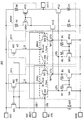
図6に本発明者が事前に検討したDC/DCコンバータの回路図を示す。 FIG. 6 shows a circuit diagram of a DC / DC converter examined in advance by the present inventor.
DC/DCコンバータ600は、外部端子としてIN,SW,PGND,AGND,FB及びCOMPを備え、外部端子の1つである入力端子INに供給される入力電圧VINを降圧して所望の出力電圧VOUTを出力端子OUTに出力する、よく知られた降圧型のスイッチングレギュレータを構成している。
The DC /
DC/DCコンバータ600は、スイッチングトランジスタ1、同期整流素子2、エラーアンプ3、発振回路装置4、合算手段5、PWMコンパレータ6及び駆動制御回路7を備える。
The DC /
さらに、DC/DCコンバータ600の外部に設けた各外部端子を介して、入力電圧VIN、インダクタL41、キャパシタC41〜C42、抵抗R41〜R43及び接地電位GNDが接続されている。DC/DCコンバータ600は、これに付設した外部端子に接続されるインダクタ、キャパシタ、抵抗等の受動素子の働きによって降圧動作を行う。
Further, the input voltage VIN, the inductor L41, the capacitors C41 to C42, the resistors R41 to R43, and the ground potential GND are connected via the external terminals provided outside the DC /
入力電圧VINは、例えば10V〜15Vに選ばれた直流電圧であり、入力端子INに印加される。なお、出力電圧VOUTは例えば5V前後に設定されている。スイッチングトランジスタ1のソースは、入力端子INに接続される。スイッチングトランジスタ1のドレインはスイッチング端子SW及び同期整流素子2のドレインに接続される。同期整流素子2のソースは、接地端子PGNDを介して接地電位GNDに接続されている。接地端子AGNDは、接地端子PGNDと同様に接地電位GNDに接続されるが、接地端子PGNDとは別に用意されている。これは、比較的小電流が流れ接地端子AGNDに接続されているエラーアンプ3、発振回路装置4、PWMコンパレータ6、および駆動制御回路7等の回路動作が比較的大きな電流が流れる接地端子PGNDの電位の変動の影響を受けないようにするためである。
The input voltage VIN is, for example, a DC voltage selected from 10V to 15V, and is applied to the input terminal IN. The output voltage VOUT is set to, for example, around 5V. The source of the
なお、スイッチングトランジスタ1は、pチャネル形MOSトランジスタを、同期整流素子2はnチャネル形MOSトランジスタとしたが、これらの組み合わせに限定されない。たとえば、スイッチングトランジスタ1はnMOSトランジスタであってもよいし、同期整流素子2はダイオードに置き換えることもできる。
The
インダクタL41の一端はスイッチング端子SWに接続されている。インダクタL41の他端は出力端子OUT及びキャパシタC41の一端に、キャパシタC41の他端はそれぞれ接地電位GNDに接続されている。 One end of the inductor L41 is connected to the switching terminal SW. The other end of the inductor L41 is connected to the output terminal OUT and one end of the capacitor C41, and the other end of the capacitor C41 is connected to the ground potential GND.
出力端子OUTと接地電位GNDとの間に直列接続される抵抗R41及びR42は帰還電圧生成回路として動作する。抵抗R41及びR42は、互いの共通接続ノードに帰還電圧VFBを出力する。帰還電圧VFBは第1入力端子IN1(フィードバック端子FB)を介して、エラーアンプ3の反転入力端子(−)に入力される。
The resistors R41 and R42 connected in series between the output terminal OUT and the ground potential GND operate as a feedback voltage generation circuit. The resistors R41 and R42 output a feedback voltage VFB to each other's common connection node. The feedback voltage VFB is input to the inverting input terminal (−) of the
エラーアンプ3の非反転入力端子(+)には基準電圧VREF、反転入力端子(−)には帰還電圧VFBがそれぞれ入力される。エラーアンプ3は入力端子が受け入れる電圧に応じた誤差信号Verrを、PWMコンパレータ6の反転入力端子(−)に出力する。また、エラーアンプ3の出力端子は位相補償端子COMPを介して抵抗R43及びキャパシタC42が接続されている。
A reference voltage VREF is input to the non-inverting input terminal (+) of the
発振回路装置4で生成されるクロック信号CLKは、駆動制御回路7に入力される。また、発振回路4は後段の合算手段5にスロープ信号SLOPEを出力する。スロープ信号SLOPEはクロック信号CLKに追随して周期が変化する例えば三角波形または鋸波形である。 The clock signal CLK generated by the oscillation circuit device 4 is input to the drive control circuit 7. Further, the oscillation circuit 4 outputs the slope signal SLOPE to the summing means 5 in the subsequent stage. The slope signal SLOPE is, for example, a triangular waveform or a saw waveform whose period changes following the clock signal CLK.
合算手段5ではスロープ信号SLOPE及びスイッチング電流ISWに応じた電圧成分を合算し、PWMコンパレータ6の非反転入力端子(+)に出力する。合算手段5は、DC/DCコンバータ600を電流帰還形と構成するために用意したものであるので、電圧帰還形で用いる場合には不要となる。
In the summing means 5, the voltage components corresponding to the slope signal SLOPE and the switching current ISW are summed and output to the non-inverting input terminal (+) of the PWM comparator 6. Since the summing means 5 is prepared to configure the DC /
PWMコンパレータ6は、リセット信号RESETを駆動制御回路7に出力する。駆動制御回路7は、スイッチングトランジスタ1及び同期整流素子2のゲートに接続されている。
The PWM comparator 6 outputs a reset signal RESET to the drive control circuit 7. The drive control circuit 7 is connected to the gate of the
このような構成の降圧型のDC/DCコンバータ600の動作について簡単に説明する。降圧モードにおけるDC/DCコンバータ600は、スイッチングトランジスタ1がオン状態で同期整流素子2がオフ状態である場合、入力端子INからインダクタL41を介してキャパシタC41にスイッチング電流ISWが流れ、磁気エネルギーが蓄えられる。逆にスイッチングトランジスタ1がオフ状態で同期整流素子2がオン状態である場合、同期整流素子2側からインダクタL41を介してキャパシタC41に電流が流れることにより、インダクタL41に蓄えられていた磁気エネルギーが放出される。このような動作により、入力電圧VINは降圧され、出力端子OUTから出力電圧VOUTが出力される。抵抗R41と抵抗R42は、出力端子OUTから出力される出力電圧VOUTを分圧して帰還電圧VFBを生成し、第1入力端子IN1(フィードバック端子FB)に送出する。
The operation of the step-down DC /
エラーアンプ3は、基準電圧VREFとフィードバック電圧VFBとを比較し、比較結果に応じた誤差信号Verrを出力する。フィードバック電圧VFBは、例えば、0.6V〜5Vである。
The
位相補償端子COMPと接地電位GND間に直列接続された抵抗R43及びキャパシタC42は位相補償回路として、エラーアンプ3のゲインと周波数特性を設定する。位相補償によってDC/DCコンバータ600の周波数特性が補正される。なお、位相補償回路は抵抗R43とキャパシタC42との直列回路ではなく、これらに別のキャパシタを例えば並列に接続して、いわゆる2次特性をもたせるようにしてもよい。
The resistor R43 and the capacitor C42 connected in series between the phase compensation terminal COMP and the ground potential GND set the gain and frequency characteristics of the
発振回路装置4は、クロック信号CLKを出力し、その周波数は例えば200kHz〜5MHzに選ばれる。通常、これらの範囲の中の1つの周波数でスイッチングトランジスタ1および同期整流素子2がオン/オフ制御される。例えば周波数が1MHzに設定された場合にはオンデューティ比が90%のときは、0.9μsであり、オンデューティ比が10%のときは0.1μsとなる。
The oscillator circuit device 4 outputs a clock signal CLK, and its frequency is selected to be, for example, 200 kHz to 5 MHz. Normally, the
駆動制御回路7は、発振回路装置4から出力されるクロック信号CLK及びPWMコンパレータ6から出力されるリセット信号RESETを受け、ゲート信号GP及びゲート信号GNを出力する。ゲート信号GP及びゲート信号GNにより、スイッチングトランジスタ1及び同期整流素子2を相補的にオン/オフされる。駆動制御回路7の内部には図示しない、例えばRSフリップフロップが用意されており、このRSフリップフロップのセット端子には発振回路装置4で生成されるクロック信号CLKが、リセット端子にはPWMコンパレータ6から出力されるリセット信号RESETがそれぞれ印加される。
The drive control circuit 7 receives the clock signal CLK output from the oscillation circuit device 4 and the reset signal RESET output from the PWM comparator 6, and outputs the gate signal GP and the gate signal GN. The
駆動制御回路7には、図示はしないがスイッチングトランジスタ1から同期整流素子2に向かって流れる過大な貫通電流を防止するため、デッドタイムが設けられている。デッドタイムの区間、スイッチングトランジスタ1及び同期整流素子2は共にオフ状態に置かれ貫通電流の電流経路を阻止する。
Although not shown, the drive control circuit 7 is provided with a dead time in order to prevent an excessive through current flowing from the switching
図7に、エラーアンプ3(オペアンプ)の出力電流特性を示す。図7は横軸がフィードバック電圧VFBを、縦軸がエラーアンプ出力電流Ierrをそれぞれ示している。フィードバック電圧VFBに関わらずエラーアンプ出力電流Ierrの傾きgmが一定となっている。 FIG. 7 shows the output current characteristics of the error amplifier 3 (op amp). In FIG. 7, the horizontal axis represents the feedback voltage VFB, and the vertical axis represents the error amplifier output current Irr. The slope gm of the error amplifier output current Irr is constant regardless of the feedback voltage VFB.
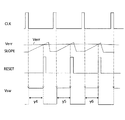
図8は、誤差信号Verrのうねりによって生じる不具合を説明するためにクロック信号CLKとスロープ信号SLOPEとリセット信号RESETとスイッチング電圧Vswを併せて示す波形図である。 FIG. 8 is a waveform diagram showing the clock signal CLK, the slope signal SLOPE, the reset signal RESET, and the switching voltage Vsw together in order to explain the problem caused by the swell of the error signal Verr.
PWMコンパレータ6の出力であるリセット信号RESETに時間的な揺らぎが発生した結果として、一定であるはずのスイッチング電圧のオン時間y7,y8,y9がばらつくことを知見した。このばらつきは出力電圧VOUTのゆらぎに影響を及ぼす。 It was found that the on-time y7, y8, y9 of the switching voltage, which should be constant, fluctuates as a result of the temporal fluctuation of the reset signal RESET which is the output of the PWM comparator 6. This variation affects the fluctuation of the output voltage VOUT.
本発明者が事前検討したオペアンプ(エラーアンプ3)をDC/DCコンバータに採用すると、応答性をよくするためにオペアンプのトランスコンダクタンスは高めに設定されており、またトランスコンダクタンスは電圧に依らず一定のため、基準電圧VREFを行き過ぎたり戻ったりを繰り返すことがあり、誤差信号Verrの波形がうねることが起こりうる。 When the operational amplifier (error amplifier 3) examined in advance by the present inventor is adopted in the DC / DC converter, the transconductivity of the operational amplifier is set high in order to improve the responsiveness, and the transconductance is constant regardless of the voltage. Therefore, the reference voltage VREF may be repeatedly passed and returned, and the waveform of the error signal Verr may undulate.
特許文献1に記載されたオペアンプのスルーレート増大方法では、しきい値の調整が非常に難しく、細かい調整ができないという不具合が起こりうる。
In the method for increasing the slew rate of an operational amplifier described in
特許文献2に記載されたオペアンプのバイアス電流可変回路では、バイアス電流を増減する為に判定回路が必要となり回路面積の増大を招く恐れがある。 In the bias current variable circuit of the operational amplifier described in Patent Document 2, a determination circuit is required to increase or decrease the bias current, which may lead to an increase in the circuit area.
特許文献3に記載されたオペアンプのバイアス電流可変回路では、バイアス電流を増減する為に判定回路が必要となり回路面積の増大を招く恐れがある。
In the bias current variable circuit of the operational amplifier described in
本発明は、上記問題点を克服する為になされたものであり、その目的は、エラーアンプの制御において、基準電圧VREF付近における誤差信号Verrのうねりを抑制し、スイッチング電圧Vswのオン/オフ時間のばらつきを抑制することである。 The present invention has been made to overcome the above problems, and an object of the present invention is to suppress the swell of the error signal Verr in the vicinity of the reference voltage VREF in the control of the error amplifier, and to turn on / off the switching voltage Vsw. It is to suppress the variation of.
本書で第1主電極とはMOSトランジスタにおいてはソースが、バイポーラトランジスタにおいてはエミッタがそれぞれ対応する。また第2主電極とはMOSトランジスタにおいてはドレインが、バイポーラトランジスタにおいてはコレクタがそれぞれ対応する。また制御電極とはMOSトランジスタにおいてはゲートが、バイポーラトランジスタにおいてはベースがそれぞれ対応する。また、本書で物理的サイズが同じとは、MOSトランジスタにおいてはゲートのチャネル長、チャネル幅が同じであることを指し、バイポーラトランジスタにおいてはエミッタ面積が等しいことを指す。 In this document, the first main electrode corresponds to the source in the MOS transistor and the emitter in the bipolar transistor. Further, the second main electrode corresponds to the drain in the MOS transistor and the collector in the bipolar transistor. The control electrode corresponds to the gate in the MOS transistor and the base in the bipolar transistor. Further, in this document, the same physical size means that the gate channel length and channel width are the same in the MOS transistor, and that the emitter area is the same in the bipolar transistor.
本発明のオペアンプの一態様は、第1主電極、第2主電極及び制御電極を有する第1トランジスタ、第2トランジスタ、第3トランジスタ及び第4トランジスタを備え、前記第1トランジスタと前記第2トランジスタの前記第1主電極は共通に接続され第1差動対トランジスタを形成し第1電流源に接続され、前記第3トランジスタと前記第4トランジスタの前記第1主電極は共通に接続され第2差動対トランジスタを形成し第2電流源に接続され、前記第1トランジスタと前記第4トランジスタの前記制御電極は共通に接続され第1入力信号が印加される第1入力端子に接続され、前記第2トランジスタと前記第3トランジスタの前記制御電極は共通に接続され第2入力信号が印加される第2入力端子に接続され、前記第1トランジスタの前記第2主電極と前記第3トランジスタの前記第2主電極は共通に接続されて第1回路点に接続され、前記第2トランジスタの前記第2主電極と前記第4トランジスタの前記第2主電極は共通に接続されて第2回路点に接続され、前記第1回路点及び前記第2回路点にそれぞれ前記第1入力信号と前記第2入力信号との第1差分信号及び第2差分信号を取り出す。 One aspect of the operational amplifier of the present invention includes a first transistor, a second transistor, a third transistor, and a fourth transistor having a first main electrode, a second main electrode, and a control electrode, and the first transistor and the second transistor are provided. The first main electrode is connected in common to form a first differential pair transistor and is connected to a first current source, and the third transistor and the first main electrode of the fourth transistor are commonly connected and second. A differential pair transistor is formed and connected to a second current source, and the control electrodes of the first transistor and the fourth transistor are commonly connected and connected to a first input terminal to which a first input signal is applied. The second transistor and the control electrode of the third transistor are commonly connected and connected to a second input terminal to which a second input signal is applied, and the second main electrode of the first transistor and the control electrode of the third transistor are described. The second main electrode is commonly connected and connected to the first circuit point, and the second main electrode of the second transistor and the second main electrode of the fourth transistor are commonly connected to the second circuit point. It is connected, and the first difference signal and the second difference signal of the first input signal and the second input signal are taken out to the first circuit point and the second circuit point, respectively.
また本発明のオペアンプの別の一態様は、前記第1トランジスタと前記第2トランジスタの物理的サイズは同じ第1のサイズであり、前記第3トランジスタと前記第4トランジスタの物理的サイズは同じであるも前記第1のサイズと異なる第2のサイズである。 In another aspect of the operational amplifier of the present invention, the first transistor and the second transistor have the same physical size, and the third transistor and the fourth transistor have the same physical size. There is a second size that is different from the first size.
また本発明のオペアンプの別の一態様は、前記第1トランジスタ,前記第2トランジスタ,前記第3トランジスタ及び前記第4トランジスタはMOSトランジスタで構成され、前記MOSトランジスタのゲートチャネル長,ゲートチャネル幅の少なくとも一方を異ならせて前記第1のサイズと前記第2のサイズが構成されている。 Further, another aspect of the operational amplifier of the present invention is that the first transistor, the second transistor, the third transistor, and the fourth transistor are composed of MOS transistors, and the gate channel length and gate channel width of the MOS transistor are different. The first size and the second size are configured by at least one of them being different.
また本発明のオペアンプの別の一態様は、前記第1電流源と前記第2電流源で生成される電流の大きさは異なっている。 Further, in another aspect of the operational amplifier of the present invention, the magnitudes of the currents generated by the first current source and the second current source are different.
また本発明のオペアンプの別の一態様は、前記第1差分信号及び前記第2差分信号はそれぞれ前記第1回路点及び前記第2回路点に電流に変換されて取り出される。 In another aspect of the operational amplifier of the present invention, the first difference signal and the second difference signal are converted into currents at the first circuit point and the second circuit point, respectively, and taken out.
また本発明のオペアンプの別の一態様は、前記第1差分信号と前記第2差分信号は加算器で加算されて合成差分信号として出力端子から取り出される。 In another aspect of the operational amplifier of the present invention, the first difference signal and the second difference signal are added by an adder and taken out from the output terminal as a combined difference signal.
また本発明のオペアンプの別の一態様は、前記第1入力信号と前記第2入力信号の差分が比較的小さいときのトランスコンダクタンスは、前記第1入力信号と前記第2入力信号の差分が比較的大きいときのトランスコンダクタンスよりも小さい。 Further, in another aspect of the operational amplifier of the present invention, when the difference between the first input signal and the second input signal is relatively small, the transconductance is such that the difference between the first input signal and the second input signal is compared. It is smaller than the transconductance when it is large.
また本発明の別の発明であるDC/DCコンバータは、入力電圧から出力電圧を生成するためにオン/オフされるスイッチング手段と、前記出力電圧に応じたフィードバック電圧と基準電圧との差に応じた誤差信号を生成するエラーアンプと、クロック信号と三角波または鋸波のスロープ信号を生成する発振回路装置と、前記スロープ信号と前記誤差信号とを比較して、パルス幅が変調されたPWM信号を出力するPWMコンパレータと、前記クロック信号と前記PWMコンパレータからの出力信号を受け、前記スイッチング手段を制御する駆動制御回路とを備え、前記エラーアンプは、上記オペアンプのいずれか1つの態様のものを用いる。 Further, the DC / DC converter which is another invention of the present invention corresponds to the switching means which is turned on / off to generate the output voltage from the input voltage and the difference between the feedback voltage and the reference voltage according to the output voltage. An error amplifier that generates an error signal, an oscillation circuit device that generates a clock signal and a triangular wave or saw wave slope signal, and a PWM signal whose pulse width is modulated by comparing the slope signal with the error signal. The error amplifier includes a PWM comparator that outputs a voltage, a drive control circuit that receives the clock signal and an output signal from the PWM comparator, and controls the switching means, and uses one of the operational amplifiers as the error amplifier. ..
この発明によれば、エラーアンプの基準電圧付近の誤差信号Verrのうねりを抑制することができる。 According to the present invention, it is possible to suppress the waviness of the error signal Verr near the reference voltage of the error amplifier.
以下、本発明の実施の形態について図面を参照して説明する。 Hereinafter, embodiments of the present invention will be described with reference to the drawings.
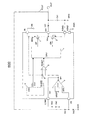
図1は、本発明に係るエラーアンプ3Aの構成の一例を示す。図6のエラーアンプ3をエラーアンプ3Aに置き換えたものが本発明に係るDC/DCコンバータとなり、その他の回路は図6と同じである。
FIG. 1 shows an example of the configuration of the
図1において、電流源ISETの一端は接地電位GNDに接続されており、その他端はMOSトランジスタM1のドレインに接続されており、そのソースは電源電位VCCに接続されている。またMOSトランジスタM1〜M3のゲートはMOSトランジスタM1のドレインに共通接続されている。MOSトランジスタM2,M3のソースはMOSトランジスタM1のソースと同様に電源電位VCCに接続されている。すなわちMOSトランジスタM1〜M3及び電流源ISETによってよく知られたカレントミラー回路を形成している。 In FIG. 1, one end of the current source ISET is connected to the ground potential GND, the other end is connected to the drain of the MOS transistor M1, and the source is connected to the power supply potential VCS. Further, the gates of the MOS transistors M1 to M3 are commonly connected to the drain of the MOS transistors M1. The sources of the MOS transistors M2 and M3 are connected to the power supply potential VCS in the same manner as the source of the MOS transistors M1. That is, the MOS transistors M1 to M3 and the current source ISET form a well-known current mirror circuit.
MOSトランジスタM2のドレインはMOSトランジスタM4とMOSトランジスタM5のソース(第1主電極)に接続されており、MOSトランジスタM4のゲート(制御電極)は第1入力端子IN1(フィードバック端子FB)に接続されており、MOSトランジスタM5のゲート(制御電極)は第2入力端子IN2(基準端子REF)に接続されている。 The drain of the MOS transistor M2 is connected to the source (first main electrode) of the MOS transistor M4 and the MOS transistor M5, and the gate (control electrode) of the MOS transistor M4 is connected to the first input terminal IN1 (feedback terminal FB). The gate (control electrode) of the MOS transistor M5 is connected to the second input terminal IN2 (reference terminal REF).
MOSトランジスタM4,M5の物理的サイズは同じであり、両者MOSトランジスタによって第1差動対トランジスタDFA1を形成している。
MOSトランジスタM4のドレイン(第2主電極)は抵抗R1の一端とMOSトランジスタM6のドレインに接続され第1回路点CP1を形成しており、MOSトランジスタM5のドレイン(第2主電極)は抵抗R2の一端とMOSトランジスタM7のドレインに接続され第2回路点CP2を形成しており、抵抗R1の他端は抵抗R2の他端とMOSトランジスタM6のゲートとMOSトランジスタM7のゲートと共通接続されている。
The physical sizes of the MOS transistors M4 and M5 are the same, and the first differential pair transistor DFA1 is formed by both MOS transistors.
The drain (second main electrode) of the MOS transistor M4 is connected to one end of the resistor R1 and the drain of the MOS transistor M6 to form the first circuit point CP1, and the drain (second main electrode) of the MOS transistor M5 is the resistor R2. Is connected to one end of the MOS transistor M7 to form the second circuit point CP2, and the other end of the resistor R1 is commonly connected to the other end of the resistor R2, the gate of the MOS transistor M6, and the gate of the MOS transistor M7. There is.
第1回路点CP1には第1入力端子IN1(フィードバック端子FB)と第2入力端子IN2(基準端子REF)との第1差分信号が電流に変換されて取り出され、第2回路点CP2には第1入力端子IN1(フィードバック端子FB)と第2入力端子IN2(基準端子REF)との第2差分信号が電流に変換されて取り出される。 At the first circuit point CP1, the first difference signal between the first input terminal IN1 (feedback terminal FB) and the second input terminal IN2 (reference terminal REF) is converted into a current and taken out, and at the second circuit point CP2. The second difference signal between the first input terminal IN1 (feedback terminal FB) and the second input terminal IN2 (reference terminal REF) is converted into a current and taken out.
MOSトランジスタM6とMOSトランジスタM7のソースは接地電位GNDに接続されている。 The sources of the MOS transistor M6 and the MOS transistor M7 are connected to the ground potential GND.
MOSトランジスタM3のドレインはMOSトランジスタM8とMOSトランジスタM9のソース(第1主電極)に接続されており、MOSトランジスタM9のゲート(制御電極)は第1入力端子IN1(フィードバック端子FB)に接続されており、MOSトランジスタM8のゲート(制御電極)は第2入力端子IN2(基準端子REF)に接続されている。 The drain of the MOS transistor M3 is connected to the source (first main electrode) of the MOS transistor M8 and the MOS transistor M9, and the gate (control electrode) of the MOS transistor M9 is connected to the first input terminal IN1 (feedback terminal FB). The gate (control electrode) of the MOS transistor M8 is connected to the second input terminal IN2 (reference terminal REF).
MOSトランジスタM8,M9の物理的サイズは同じであり、両者MOSトランジスタによって第2差動対トランジスタDFA2を形成している。 The physical sizes of the MOS transistors M8 and M9 are the same, and the second differential pair transistor DFA2 is formed by both MOS transistors.
MOSトランジスタM8のドレイン(第2主電極)は抵抗R3の一端とMOSトランジスタM10のドレインに接続され第1回路点CP1を形成しており、MOSトランジスタM9のドレイン(第2主電極)は抵抗R4の一端とMOSトランジスタM11のドレインに接続され第2回路点CP2を形成しており、抵抗R3の他端は抵抗R4の他端とMOSトランジスタM10のゲートとMOSトランジスタM11のゲートと共通接続されている。 The drain (second main electrode) of the MOS transistor M8 is connected to one end of the resistor R3 and the drain of the MOS transistor M10 to form the first circuit point CP1, and the drain (second main electrode) of the MOS transistor M9 is the resistor R4. Is connected to one end of the MOS transistor M11 to form the second circuit point CP2, and the other end of the resistor R3 is commonly connected to the other end of the resistor R4, the gate of the MOS transistor M10, and the gate of the MOS transistor M11. There is.
MOSトランジスタM10とMOSトランジスタM11のソースは接地電位GNDに接続されている。 The sources of the MOS transistor M10 and the MOS transistor M11 are connected to the ground potential GND.
MOSトランジスタM6のドレインはMOSトランジスタM10のドレインとMOSトランジスタM12のゲートに接続されており、MOSトランジスタM7のドレインはMOSトランジスタM11のドレインとMOSトランジスタM13のゲートに接続されている。 The drain of the MOS transistor M6 is connected to the drain of the MOS transistor M10 and the gate of the MOS transistor M12, and the drain of the MOS transistor M7 is connected to the drain of the MOS transistor M11 and the gate of the MOS transistor M13.
MOSトランジスタM13のソースは抵抗R5の一端に接続されており、抵抗R5の他端は接地電位GNDに接続されている。MOSトランジスタM13のドレインは、MOSトランジスタM14のドレインとゲートに接続されており、MOSトランジスタM14のソースは抵抗R6の一端と接続されており、抵抗R6の他端は電源電位VCCに接続されている。 The source of the MOS transistor M13 is connected to one end of the resistor R5, and the other end of the resistor R5 is connected to the ground potential GND. The drain of the MOS transistor M13 is connected to the drain of the MOS transistor M14 and the gate, the source of the MOS transistor M14 is connected to one end of the resistor R6, and the other end of the resistor R6 is connected to the power supply potential VCS. ..
MOSトランジスタM12のソースは抵抗R7の一端が接続されており、抵抗R7の他端は接地電位GNDに接続されている。MOSトランジスタM12のドレインは、MOSトランジスタM15のドレイン及び電流出力端子OUT1に接続されている。MOSトランジスタM15のソースは抵抗R8の一端と接続されており、抵抗R8の他端は電源電位VCCに接続されている。MOSトランジスタM15のゲートはMOSトランジスタM14のゲートに接続されている。 One end of the resistor R7 is connected to the source of the MOS transistor M12, and the other end of the resistor R7 is connected to the ground potential GND. The drain of the MOS transistor M12 is connected to the drain of the MOS transistor M15 and the current output terminal OUT1. The source of the MOS transistor M15 is connected to one end of the resistor R8, and the other end of the resistor R8 is connected to the power supply potential VCS. The gate of the MOS transistor M15 is connected to the gate of the MOS transistor M14.
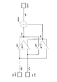
エラーアンプ3Aは簡潔に言うと、トランスコンダクタンスの大きさが違う2つのオペアンプが合成された構成となっている。ここで2つのオペアンプとは、MOSトランジスタM2,M4,M5,M6,M7で構成される第1オペアンプOP1とMOSトランジスタM3,M8,M9,M10,M11で構成される第2オペアンプOP2である。
To put it simply, the
MOSトランジスタM2は、カレントミラーの基準となるMOSトランジスタM1の例えば5倍のサイズを有しているのに対し、MOSトランジスタM3は例えば2倍のサイズを有している。この違いにより第1オペアンプOP1と第2オペアンプOP2に供給する電流に差を持たしている。MOSトランジスタM2及びMOSトランジスタM3は本書においてそれぞれ第1電流源及び第2電流源に対応する。第1電流源は電流I2を生成し、第2電流源は電流I3を生成する。 The MOS transistor M2 has, for example, five times the size of the MOS transistor M1 that serves as a reference for the current mirror, whereas the MOS transistor M3 has, for example, twice the size. Due to this difference, there is a difference in the current supplied to the first operational amplifier OP1 and the second operational amplifier OP2. The MOS transistor M2 and the MOS transistor M3 correspond to a first current source and a second current source, respectively, in this document. The first current source produces the current I2 and the second current source produces the current I3.
またMOSトランジスタM4,M5とMOSトランジスタM8,M9の物理的サイズは異なっている。例えばMOSトランジスタM4,M5のゲートチャネル幅Wが10μm,ゲートチャネル長Lが3μmであるのに対し、例えばMOSトランジスタM8,M9のゲートチャネル幅Wが5μm,ゲートチャネル長Lが1μmである。この物理的サイズの違いによりトランスコンダクタンスgmに差を持たせている。 Further, the physical sizes of the MOS transistors M4 and M5 and the MOS transistors M8 and M9 are different. For example, the gate channel width W of the MOS transistors M4 and M5 is 10 μm and the gate channel length L is 3 μm, whereas the gate channel width W of the MOS transistors M8 and M9 is 5 μm and the gate channel length L is 1 μm. Due to this difference in physical size, there is a difference in transconductance gm.
本発明では、ゲートチャネル幅W,ゲートチャネル長Lの両方を異ならせているが、設定するトランスコンダクタンスによっては少なくとも一方を異ならせればよい。 In the present invention, both the gate channel width W and the gate channel length L are different, but at least one may be different depending on the transconductance to be set.
MOSトランジスタM12〜M15及びR5〜R8は加算器Adderを構成する。加算器Adderは第1回路点CP1の出力である第1差分信号及び第2回路点CP2の出力である第2差分信号を加算して合成差分信号として電流出力端子OUT1に出力する。 MOS transistors M12 to M15 and R5 to R8 form an adder adder. The adder Adder adds the first difference signal which is the output of the first circuit point CP1 and the second difference signal which is the output of the second circuit point CP2, and outputs the combined difference signal to the current output terminal OUT1.
図2は、第1オペアンプOP1と第2オペアンプOP2の接続概念図を示す。第1オペアンプOP1の第1トランスコンダクタンスgm1と第2オペアンプOP2の第2トランスコンダクタンスgm2が加算器Adderで加算されて出力されることとなる。 FIG. 2 shows a conceptual diagram of connection between the first operational amplifier OP1 and the second operational amplifier OP2. The first transconductance gm1 of the first operational amplifier OP1 and the second transconductance gm2 of the second operational amplifier OP2 are added by the adder Adder and output.
第1オペアンプOP1と第2オペアンプOP2の出力電流は同一ではない。その差はMOSトランジスタM2,M3の比によるカレントミラー電流の差、およびMOSトランジスタM4,M5とMOSトランジスタM8,M9のゲートチャネル長L,ゲートチャネル幅Wの違いで構成されている。 The output currents of the first operational amplifier OP1 and the second operational amplifier OP2 are not the same. The difference is composed of the difference in the current mirror current due to the ratio of the MOS transistors M2 and M3, and the difference in the gate channel length L and the gate channel width W of the MOS transistors M4 and M5 and the MOS transistors M8 and M9.
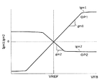
図3は、図1に示したエラーアンプ3Aのトランスコンダクタンス特性を示す。縦軸が第1オペアンプOP1と第2オペアンプOP2の出力電流Igm1,Igm2を示している。ここで出力電流Igm1はMOSトランジスタM5のドレインから出力される。出力電流Igm2はMOSトランジスタM9のドレインから出力される。なお、第1オペアンプOP1のMOSトランジスタM4のドレイン及び第2オペアンプOP2のMOSトランジスタM8のドレインからもそれぞれ出力電流が出力されるが、これらの出力電流は説明の便宜上及び図面の煩雑さを避けるために割愛している。
FIG. 3 shows the transconductance characteristics of the
横軸は、第1入力端子IN1に印加されるフィードバック電圧VFBを変化させ第2入力端子IN2に印加される基準電圧VREFを固定したときを示している。 The horizontal axis shows the case where the feedback voltage VFB applied to the first input terminal IN1 is changed and the reference voltage VREF applied to the second input terminal IN2 is fixed.
第1オペアンプOP1の出力電流Igm1は第2オペアンプOP2の出力電流Igm2よりも大きく設定されている。また、出力電流Igm1と出力電流Igm2の電流特性の傾きは互いに逆になるように設定している。 The output current Igm1 of the first operational amplifier OP1 is set to be larger than the output current Igm2 of the second operational amplifier OP2. Further, the slopes of the current characteristics of the output current Igm1 and the output current Igm2 are set to be opposite to each other.
第1オペアンプOP1の出力電流Igm1は主にMOSトランジスタM2,M4,M5で設定されている。MOSトランジスタM2により最大電流が、MOSトランジスタM4,M5により最大電流すなわち第1トランスコンダクタンスgm1が決定される。第1トランスコンダクタンスgm1は、次式で表わされる。 The output current Igm1 of the first operational amplifier OP1 is mainly set by the MOS transistors M2, M4, and M5. The maximum current is determined by the MOS transistors M2, and the maximum current, that is, the first transconductance gm1 is determined by the MOS transistors M4 and M5. The first transconductance gm1 is expressed by the following equation.
gm1=ΔIgm1/Δ(VFB−VREF) gm1 = ΔIgm1 / Δ (VFB-VREF)
同様に第2オペアンプOP2の出力電流Igm2は主にMOSトランジスタM3,M8,M9で設定されている。MOSトランジスタM3により最大電流が、MOSトランジスタM8,M9により最大電流すなわち第2トランスコンダクタンスgm2が決定される。第2トランスコンダクタンスgm2は、次式で表わされる。 Similarly, the output current Igm2 of the second operational amplifier OP2 is mainly set by the MOS transistors M3, M8, and M9. The maximum current is determined by the MOS transistors M3, and the maximum current, that is, the second transconductance gm2 is determined by the MOS transistors M8 and M9. The second transconductance gm2 is expressed by the following equation.
gm2=ΔIgm2/Δ(VFB−VREF) gm2 = ΔIgm2 / Δ (VFB-VREF)
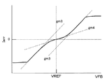
これら第1オペアンプOP1と第2オペアンプOP2のトランスコンダクタンス特性を加算することで、図4の合成特性を実現する。 By adding the transconductance characteristics of the first operational amplifier OP1 and the second operational amplifier OP2, the composite characteristics of FIG. 4 are realized.
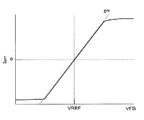
図4は、エラーアンプ3Aの出力電流Ierrを示している。横軸がフィードバック電圧VFBを示し、縦軸が出力電流Ierrを示している。
フィードバック電圧VFBが基準電圧VREFから離れたところではトランスコンダクタンスが大きくなっており、基準電圧VREF付近ではトランスコンダクタンスが小さくなっている。エラーアンプ3Aの出力電圧が設定電圧付近では、トランスコンダクタンスを下げて安定性を確保し、出力電圧が設定電圧から離れるとトランスコンダクタンスを上げてエラーアンプ3Aの帰還スピードをアップすることとなる。
すなわち基準電圧VREFから遠い電圧にある時は急速に、近いところにある時は緩やかに制御されることとなる。これにより基準電圧VREF付近における波形のうねりが小さくなる。
FIG. 4 shows the output current Ierr of the
The transconductance is large when the feedback voltage VFB is separated from the reference voltage VREF, and is small near the reference voltage VREF. When the output voltage of the
That is, the voltage is controlled rapidly when the voltage is far from the reference voltage VREF, and gently when the voltage is close to the reference voltage VREF. As a result, the waviness of the waveform near the reference voltage VREF is reduced.
図4におけるエラーアンプ3A全体のトランスコンダクタンスgm3,gm4は第1オペアンプOP1と第2オペアンプOP2のトランスコンダクタンスの組み合わせにより自由に設計可能である。要求するエラーアンプ3Aの入出力特性にあわせて図1の第1差動対トランジスタDFA1と第2差動対トランジスタDFA2のトランスコンダクタンスの大きさを設定すればよい。第1差動対トランジスタDFA1のトランスコンダクタンスはMOSトランジスタM4,M5のゲートチャネル長Lとゲートチャネル幅Wとの比W/Lと電流I2との積(W/L)I2を適宜設定し、第2差動対トランジスタDFA2のトランスコンダクタンスはMOSトランジスタM8,M9のゲートチャネル長Lとゲートチャネル幅Wとの比W/Lと電流I3との積(W/L)I3を適宜設定して、それぞれ決定すればよい。
The transconductance gm3 and gm4 of the
なお、出力端子OUTに発生する出力電圧VOUTのばらつきが±数%の時は、トランスコンダクタンスが小さい区間も基準電圧VREF±数%にするとよい。そうすることで、出力電圧VOUTが安定する区間と基準電圧VREF付近における波形のうねりの小さくなる区間が一致することとなる。 When the variation of the output voltage VOUT generated at the output terminal OUT is ± several%, the reference voltage VREF ± several% may be set even in the section where the transconductance is small. By doing so, the section in which the output voltage VOUT is stable and the section in which the waviness of the waveform becomes small in the vicinity of the reference voltage VREF coincide with each other.
出力電流の最大値及び最小値は図1の抵抗R1,R2,R3及びR4の大きさで決定される。第1オペアンプOP1のMOSトランジスタM4とMOSトランジスタM5がショートしないように抵抗R1及び抵抗R2は挿入されている。この抵抗値を小さくすることで出力電流を小さくすることができる。逆に抵抗値を大きくすることで出力電流を最大限出力することができる。
第2オペアンプOP2も同様であり、MOSトランジスタM8とMOSトランジスタM9がショートしないように抵抗R3及び抵抗R4は挿入されている。
The maximum and minimum values of the output current are determined by the magnitudes of the resistors R1, R2, R3 and R4 in FIG. The resistors R1 and R2 are inserted so that the MOS transistor M4 and the MOS transistor M5 of the first operational amplifier OP1 are not short-circuited. The output current can be reduced by reducing this resistance value. On the contrary, the output current can be maximized by increasing the resistance value.
The same applies to the second operational amplifier OP2, and the resistors R3 and R4 are inserted so that the MOS transistor M8 and the MOS transistor M9 are not short-circuited.
また、出力電流の最大値及び最小値は、図1の抵抗R5,R6,R7及びR8の大きさでも決定される。この出力電流は例えば出力端子OUTが地絡した後の復帰時のオーバーシュート電流の発生につながるので適正に調整される必要がある。例えば出力電流は±20μAに設定される。 The maximum and minimum values of the output current are also determined by the magnitudes of the resistors R5, R6, R7 and R8 of FIG. This output current, for example, leads to the generation of an overshoot current at the time of recovery after the output terminal OUT has a ground fault, and therefore needs to be adjusted appropriately. For example, the output current is set to ± 20 μA.
図5に本発明における、誤差信号Verrとクロック信号CLKとスロープ信号SLOPEとリセット信号RESETとスイッチング電圧Vswの波形を示す。 FIG. 5 shows the waveforms of the error signal Verr, the clock signal CLK, the slope signal SLOPE, the reset signal SETET, and the switching voltage Vsw in the present invention.
誤差信号Verrのうねりが図8と比較して小さくなっており、リセット信号RESETが等間隔になっていることがわかる。その結果として、スイッチング電圧Vswの時間的揺らぎも解消されており、オン時間y4=y5=y6が成り立っている。この結果、出力電圧の揺らぎが抑制されることとなる。 It can be seen that the swell of the error signal Verr is smaller than that of FIG. 8, and the reset signal RESET is evenly spaced. As a result, the temporal fluctuation of the switching voltage Vsw is also eliminated, and the on-time y4 = y5 = y6 is established. As a result, fluctuations in the output voltage are suppressed.
本発明は、本例で示したMOSトランジスタで構成されるオペアンプにこだわらない。バイポーラトランジスタで構成されるオペアンプにおいても同様のことが可能である。バイポーラトランジスタのオペアンプの場合も同様に、差動入力段に流す電流値と差動入力段のエミッタ面積を変更することで実現可能である。
また本発明においてはオペアンプ2つを加算する構成で説明を行ったが、加算されるオペアンプは2つ以上であればいくつでも構わない。要求されるトランスコンダクタンスに応じて組み合わせばよい。
The present invention is not limited to the operational amplifier composed of the MOS transistors shown in this example. The same can be done with an operational amplifier composed of bipolar transistors. Similarly, in the case of a bipolar transistor operational amplifier, it can be realized by changing the current value flowing through the differential input stage and the emitter area of the differential input stage.
Further, in the present invention, the configuration in which two operational amplifiers are added has been described, but any number of operational amplifiers may be added as long as they are two or more. It may be combined according to the required transconductance.
本発明は、オペアンプによる基準電位付近におけるうねりを防止するものである。そのため、本発明は、産業上の利用可能性は極めて高い。 The present invention prevents swells near a reference potential due to an operational amplifier. Therefore, the present invention has extremely high industrial applicability.
1 スイッチングトランジスタ
2 同期整流素子
3 エラーアンプ
3A エラーアンプ
4 発振回路装置
5 合算手段
6 PWMコンパレータ
7 駆動制御回路
600 DC/DCコンバータ
Adder 加算器
AGND 接地端子
C41,C42 キャパシタ
CLK クロック信号
CP1 第1回路点
CP2 第2回路点
DFA1 第1差動対トランジスタ
DFA2 第2差動対トランジスタ
FB フィードバック端子
gm1 第1トランスコンダクタンス
gm2 第2トランスコンダクタンス
gm3 トランスコンダクタンス
gm4 トランスコンダクタンス
GN ゲート信号
GND 接地電位
GP ゲート信号
I2 電流
I3 電流
Ierr 出力電流
Igm1 出力電流
Igm2 出力電流
IN 入力端子
IN1 第1入力端子
IN2 第2入力端子
ISET 電流源
ISW スイッチング電流
L ゲートチャネル長
L41 インダクタ
M1〜M15 MOSトランジスタ
OP1 第1オペアンプ
OP2 第2オペアンプ
OUT 出力端子
OUT1 電流出力端子
PGND 接地端子
R1〜R8,R41〜R43 抵抗
REF 基準端子
RESET リセット信号
SLOPE スロープ信号
VCC 電源電位
Verr 誤差信号
VFB フィードバック電圧
VOUT 出力電圧
VREF 基準電圧
Vsw スイッチング電圧
W ゲートチャネル幅
1 Switching transistor 2
Claims (6)
第1抵抗、第2抵抗、第3抵抗及び第4抵抗と、を備え、
前記第1トランジスタの前記第1主電極と前記第2トランジスタの前記第1主電極は共通に接続され第1差動対トランジスタを形成し第1電流源に接続され、
前記第3トランジスタの前記第1主電極と前記第4トランジスタの前記第1主電極は共通に接続され第2差動対トランジスタを形成し第2電流源に接続され、
前記第1トランジスタの前記制御電極と前記第4トランジスタの前記制御電極は共通に接続され第1入力信号が印加される第1入力端子に接続され、
前記第2トランジスタの前記制御電極と前記第3トランジスタの前記制御電極は共通に接続され第2入力信号が印加される第2入力端子に接続され、
前記第1トランジスタの前記第2主電極と前記第3トランジスタの前記第2主電極は共通に接続されて第1回路点に接続され、
前記第2トランジスタの前記第2主電極と前記第4トランジスタの前記第2主電極は共通に接続されて第2回路点に接続され、
前記第5トランジスタの前記第2主電極と前記第1抵抗の第1端は共通に接続されて前記第1回路点に接続され、
前記第6トランジスタの前記第2主電極と前記第2抵抗の第1端は共通に接続されて前記第2回路点に接続され、
前記第7トランジスタの前記第2主電極と前記第3抵抗の第1端は共通に接続されて前記第1回路点に接続され、
前記第8トランジスタの前記第2主電極と前記第4抵抗の第1端は共通に接続されて前記第2回路点に接続され、
前記第5トランジスタの前記制御電極、前記第6トランジスタの前記制御電極、前記第1抵抗の第2端及び前記第2抵抗の第2端は共通に接続され、
前記第7トランジスタの前記制御電極、前記第8トランジスタの前記制御電極、前記第3抵抗の第2端及び前記第4抵抗の第2端は共通に接続され、
前記第5トランジスタの前記第1主電極、前記第6トランジスタの前記第1主電極、前記第7トランジスタの前記第1主電極及び前記第8トランジスタの前記第1主電極は共通に接続されて接地電位に接続され、
前記第1回路点及び前記第2回路点にそれぞれ前記第1入力信号と前記第2入力信号との第1差分信号及び第2差分信号が取り出され、
前記第1トランジスタと前記第2トランジスタの物理的サイズは同じ第1のサイズであり、前記第3トランジスタと前記第4トランジスタの物理的サイズは同じであるも前記第1のサイズと異なる第2のサイズであり、
前記第1差分信号及び前記第2差分信号はそれぞれ前記第1回路点及び前記第2回路点に電流に変換されて取り出され、
前記第1差分信号と前記第2差分信号は加算器で加算されて合成差分信号として出力端子から取り出される、オペアンプ。 A first transistor having a first main electrode, a second main electrode and a control electrode, a second transistor, a third transistor , a fourth transistor , a fifth transistor, a sixth transistor, a seventh transistor and an eighth transistor,
A first resistor, a second resistor, a third resistor, and a fourth resistor are provided.
The first main electrode of the first transistor and the first main electrode of the second transistor are commonly connected to form a first differential pair transistor and are connected to a first current source.
The first main electrode of the third transistor and the first main electrode of the fourth transistor are commonly connected to form a second differential pair transistor and are connected to a second current source.
The control electrode of the first transistor and the control electrode of the fourth transistor are commonly connected and connected to a first input terminal to which a first input signal is applied.
The control electrode of the second transistor and the control electrode of the third transistor are commonly connected and connected to a second input terminal to which a second input signal is applied.
The second main electrode of the first transistor and the second main electrode of the third transistor are commonly connected and connected to the first circuit point.
The second main electrode of the second transistor and the second main electrode of the fourth transistor are commonly connected and connected to a second circuit point.
The second main electrode of the fifth transistor and the first end of the first resistor are commonly connected and connected to the first circuit point.
The second main electrode of the sixth transistor and the first end of the second resistor are commonly connected and connected to the second circuit point.
The second main electrode of the seventh transistor and the first end of the third resistor are commonly connected and connected to the first circuit point.
The second main electrode of the eighth transistor and the first end of the fourth resistor are commonly connected and connected to the second circuit point.
The control electrode of the fifth transistor, the control electrode of the sixth transistor, the second end of the first resistor, and the second end of the second resistor are commonly connected.
The control electrode of the 7th transistor, the control electrode of the 8th transistor, the second end of the third resistor, and the second end of the fourth resistor are commonly connected.
The first main electrode of the fifth transistor, the first main electrode of the sixth transistor, the first main electrode of the seventh transistor, and the first main electrode of the eighth transistor are commonly connected and grounded. Connected to the potential,
The first difference signal and the second difference signal of the first input signal and the second input signal are taken out to the first circuit point and the second circuit point, respectively.
The first transistor and the second transistor have the same physical size, and the third transistor and the fourth transistor have the same physical size but are different from the first size. Is the size
The first difference signal and the second difference signal are converted into currents at the first circuit point and the second circuit point, respectively, and taken out.
An operational amplifier in which the first difference signal and the second difference signal are added by an adder and taken out from an output terminal as a combined difference signal .
第1主電極、第2主電極及び制御電極を有する第9トランジスタ、第10トランジスタ、第11トランジスタ及び第12トランジスタと、 A ninth transistor, a tenth transistor, an eleventh transistor, and a twelfth transistor having a first main electrode, a second main electrode, and a control electrode,
第5抵抗、第6抵抗、第7抵抗及び第8抵抗と、を備え、 A fifth resistor, a sixth resistor, a seventh resistor, and an eighth resistor are provided.
前記第9トランジスタの前記制御電極は前記第1回路点に接続され、前記第9トランジスタの前記第1主電極は前記第7抵抗の第1端に接続され、前記第9トランジスタの前記第2主電極は前記出力端子に接続され、 The control electrode of the ninth transistor is connected to the first circuit point, the first main electrode of the ninth transistor is connected to the first end of the seventh resistor, and the second main electrode of the ninth transistor is connected. The electrode is connected to the output terminal and
前記第10トランジスタの前記制御電極は前記第2回路点に接続され、前記第10トランジスタの前記第1主電極は前記第5抵抗の第1端に接続され、前記第10トランジスタの前記第2主電極は前記第11トランジスタの前記第2主電極に接続され、 The control electrode of the 10th transistor is connected to the 2nd circuit point, the 1st main electrode of the 10th transistor is connected to the 1st end of the 5th resistor, and the 2nd main electrode of the 10th transistor is connected. The electrode is connected to the second main electrode of the eleventh transistor and
前記第5抵抗の前記第2端と前記第7抵抗の前記第2端は共通に接続されて前記接地電位に接続され、 The second end of the fifth resistor and the second end of the seventh resistor are commonly connected and connected to the ground potential.
前記第11トランジスタの前記制御電極と前記第12トランジスタの前記制御電極は共通に接続されて前記第11トランジスタの前記第2主電極に接続され、 The control electrode of the 11th transistor and the control electrode of the 12th transistor are commonly connected and connected to the second main electrode of the 11th transistor.
前記第12トランジスタの前記第2主電極は前記出力端に接続され、 The second main electrode of the twelfth transistor is connected to the output end and is connected to the output end.
前記第11トランジスタの前記第1主電極は前記第6抵抗の第1端に接続され、 The first main electrode of the eleventh transistor is connected to the first end of the sixth resistor.
前記第12トランジスタの前記第1主電極は前記第8抵抗の第1端に接続され、 The first main electrode of the twelfth transistor is connected to the first end of the eighth resistor.
前記第6抵抗の第2端と前記第7抵抗の第2端は共通に接続されて電源電位に接続される、請求項1〜4のいずれか一項に記載のオペアンプ。 The operational amplifier according to any one of claims 1 to 4, wherein the second end of the sixth resistor and the second end of the seventh resistor are commonly connected and connected to a power supply potential.
前記出力電圧に応じたフィードバック電圧と基準電圧との差に応じた誤差信号を生成するエラーアンプと、
クロック信号と三角波または鋸波のスロープ信号を生成する発振回路装置と、
前記スロープ信号と前記誤差信号とを比較して、パルス幅が変調されたPWM信号を出力するPWMコンパレータと、
前記クロック信号と前記PWMコンパレータからの出力信号を受け、前記スイッチング手段を制御する駆動制御回路とを備えるDC/DCコンバータであって、
前記エラーアンプは、請求項1〜5のいずれか一項に記載のオペアンプで構成されることを特徴とするDC/DCコンバータ。 Switching means that are turned on / off to generate an output voltage from the input voltage,
An error amplifier that generates an error signal according to the difference between the feedback voltage corresponding to the output voltage and the reference voltage, and an error amplifier.
An oscillator circuit that generates a clock signal and a triangular or sawtooth slope signal,
A PWM comparator that compares the slope signal with the error signal and outputs a PWM signal with a modulated pulse width.
A DC / DC converter including a drive control circuit that receives the clock signal and an output signal from the PWM comparator and controls the switching means.
The error amplifier is a DC / DC converter comprising the operational amplifier according to any one of claims 1 to 5.
Priority Applications (1)
| Application Number | Priority Date | Filing Date | Title |
|---|---|---|---|
| JP2017122182A JP6886355B2 (en) | 2017-06-22 | 2017-06-22 | Operational amplifier and DC / DC converter using it |
Applications Claiming Priority (1)
| Application Number | Priority Date | Filing Date | Title |
|---|---|---|---|
| JP2017122182A JP6886355B2 (en) | 2017-06-22 | 2017-06-22 | Operational amplifier and DC / DC converter using it |
Publications (2)
| Publication Number | Publication Date |
|---|---|
| JP2019009548A JP2019009548A (en) | 2019-01-17 |
| JP6886355B2 true JP6886355B2 (en) | 2021-06-16 |
Family
ID=65029154
Family Applications (1)
| Application Number | Title | Priority Date | Filing Date |
|---|---|---|---|
| JP2017122182A Expired - Fee Related JP6886355B2 (en) | 2017-06-22 | 2017-06-22 | Operational amplifier and DC / DC converter using it |
Country Status (1)
| Country | Link |
|---|---|
| JP (1) | JP6886355B2 (en) |
Families Citing this family (6)
| Publication number | Priority date | Publication date | Assignee | Title |
|---|---|---|---|---|
| JP7170606B2 (en) * | 2019-09-03 | 2022-11-14 | 株式会社東芝 | DC-DC converter |
| DE112020006170T5 (en) | 2019-12-17 | 2022-11-17 | Rohm Co., Ltd. | OUTPUT FEEDBACK CIRCUIT |
| US12166420B2 (en) * | 2020-03-17 | 2024-12-10 | Rohm Co., Ltd. | Output feedback control circuit and switching power supply |
| KR102713249B1 (en) * | 2022-07-12 | 2024-10-11 | 한국과학기술원 | Capacitive Wireless Power Transmission System Using Fringing Field |
| CN116224033B (en) * | 2023-03-15 | 2025-08-29 | 长沙泰科阳微电子有限公司 | Fast common-mode detection circuit for fully differential amplifiers |
| CN116317996B (en) * | 2023-05-23 | 2023-08-04 | 盈力半导体(上海)有限公司 | An error amplifier and power conversion device |
Family Cites Families (10)
| Publication number | Priority date | Publication date | Assignee | Title |
|---|---|---|---|---|
| KR960027254A (en) * | 1994-12-29 | 1996-07-22 | 조백제 | Operational Transconductance Amplifier with Good Linearity |
| US5699015A (en) * | 1996-03-19 | 1997-12-16 | Motorola, Inc. | Low voltage operational amplifier and method |
| JP3396415B2 (en) * | 1997-12-18 | 2003-04-14 | 松下電器産業株式会社 | DC feedback high-pass filter |
| JP4851192B2 (en) * | 2006-01-27 | 2012-01-11 | ルネサスエレクトロニクス株式会社 | Differential signal receiver |
| JP2008022468A (en) * | 2006-07-14 | 2008-01-31 | Sanyo Electric Co Ltd | Transconductance equipment |
| JP2011072102A (en) * | 2009-09-25 | 2011-04-07 | Rohm Co Ltd | Switching regulator |
| US8405457B2 (en) * | 2010-06-15 | 2013-03-26 | Aeroflex Colorado Springs Inc. | Amplitude-stabilized odd order pre-distortion circuit |
| JP6503663B2 (en) * | 2014-09-10 | 2019-04-24 | 住友電気工業株式会社 | Differential amplifier circuit |
| WO2017072911A1 (en) * | 2015-10-29 | 2017-05-04 | 三菱電機株式会社 | Transconductance amplifier and phase shifter |
| JP2017093159A (en) * | 2015-11-10 | 2017-05-25 | ローム株式会社 | Step-down dc/dc converter and control circuit, control method therefor, on-vehicle power supply device |
-
2017
- 2017-06-22 JP JP2017122182A patent/JP6886355B2/en not_active Expired - Fee Related
Also Published As
| Publication number | Publication date |
|---|---|
| JP2019009548A (en) | 2019-01-17 |
Similar Documents
| Publication | Publication Date | Title |
|---|---|---|
| JP6886355B2 (en) | Operational amplifier and DC / DC converter using it | |
| US7777472B2 (en) | Current detector circuit and current mode switching regulator | |
| US9454168B2 (en) | LDO regulator powered by its regulated output voltage for high PSRR | |
| TW202230070A (en) | Power conversion system, method of power conversion, and pulse width modulation controller | |
| US10168726B2 (en) | Self-adaptive startup compensation device | |
| KR20060085166A (en) | Compensation technology provides stability over a wide range of output capacitor values | |
| US12244230B2 (en) | Switched-mode power supply and control circuit for use in switched-mode power supply | |
| US12374983B2 (en) | Control device for a switching voltage regulator having improved control performance and control method | |
| TWI630781B (en) | Adaptive boot compensation method and apparatus for dc-to-dc converter | |
| JP2012130138A (en) | Switching control circuit | |
| US20150002113A1 (en) | Power supply circuit | |
| JP7199330B2 (en) | regulator circuit | |
| JP5703950B2 (en) | Voltage-current converter | |
| US20070200623A1 (en) | Amplifier, and step-down regulator and operational amplifier using the amplifier | |
| JP5141289B2 (en) | CMOS differential amplifier circuit and power supply control semiconductor integrated circuit | |
| US11699947B2 (en) | DC-DC converters with loop control | |
| JP2012032940A (en) | Power supply control circuit | |
| JP2021128530A (en) | Error amplifier and power supply circuit | |
| WO2012053133A1 (en) | Chopper amplifier, active filter, and reference frequency generating circuit | |
| JP2012034472A (en) | Power supply control circuit and power supply circuit | |
| JP4784139B2 (en) | Switching regulator and power supply system | |
| JP5094512B2 (en) | Switching regulator | |
| US20250038661A1 (en) | Semiconductor circuit device and switching regulator | |
| US20250260322A1 (en) | Switching regulator | |
| US20210281169A1 (en) | Power supply circuit |
Legal Events
| Date | Code | Title | Description |
|---|---|---|---|
| A621 | Written request for application examination |
Free format text: JAPANESE INTERMEDIATE CODE: A621 Effective date: 20200511 |
|
| A977 | Report on retrieval |
Free format text: JAPANESE INTERMEDIATE CODE: A971007 Effective date: 20210218 |
|
| A131 | Notification of reasons for refusal |
Free format text: JAPANESE INTERMEDIATE CODE: A131 Effective date: 20210302 |
|
| A521 | Request for written amendment filed |
Free format text: JAPANESE INTERMEDIATE CODE: A523 Effective date: 20210422 |
|
| TRDD | Decision of grant or rejection written | ||
| A01 | Written decision to grant a patent or to grant a registration (utility model) |
Free format text: JAPANESE INTERMEDIATE CODE: A01 Effective date: 20210511 |
|
| A61 | First payment of annual fees (during grant procedure) |
Free format text: JAPANESE INTERMEDIATE CODE: A61 Effective date: 20210514 |
|
| R150 | Certificate of patent or registration of utility model |
Ref document number: 6886355 Country of ref document: JP Free format text: JAPANESE INTERMEDIATE CODE: R150 |
|
| LAPS | Cancellation because of no payment of annual fees |