JP6876033B2 - Quantum dot based imaging detector - Google Patents
Quantum dot based imaging detector Download PDFInfo
- Publication number
- JP6876033B2 JP6876033B2 JP2018505004A JP2018505004A JP6876033B2 JP 6876033 B2 JP6876033 B2 JP 6876033B2 JP 2018505004 A JP2018505004 A JP 2018505004A JP 2018505004 A JP2018505004 A JP 2018505004A JP 6876033 B2 JP6876033 B2 JP 6876033B2
- Authority
- JP
- Japan
- Prior art keywords
- scintillation
- radiation
- detection system
- different
- radiation detection
- Prior art date
- Legal status (The legal status is an assumption and is not a legal conclusion. Google has not performed a legal analysis and makes no representation as to the accuracy of the status listed.)
- Active
Links
Images


Classifications
-
- G—PHYSICS
- G01—MEASURING; TESTING
- G01T—MEASUREMENT OF NUCLEAR OR X-RADIATION
- G01T1/00—Measuring X-radiation, gamma radiation, corpuscular radiation, or cosmic radiation
- G01T1/16—Measuring radiation intensity
- G01T1/20—Measuring radiation intensity with scintillation detectors
- G01T1/2018—Scintillation-photodiode combinations
- G01T1/20183—Arrangements for preventing or correcting crosstalk, e.g. optical or electrical arrangements for correcting crosstalk
-
- B—PERFORMING OPERATIONS; TRANSPORTING
- B82—NANOTECHNOLOGY
- B82Y—SPECIFIC USES OR APPLICATIONS OF NANOSTRUCTURES; MEASUREMENT OR ANALYSIS OF NANOSTRUCTURES; MANUFACTURE OR TREATMENT OF NANOSTRUCTURES
- B82Y15/00—Nanotechnology for interacting, sensing or actuating, e.g. quantum dots as markers in protein assays or molecular motors
-
- G—PHYSICS
- G01—MEASURING; TESTING
- G01T—MEASUREMENT OF NUCLEAR OR X-RADIATION
- G01T1/00—Measuring X-radiation, gamma radiation, corpuscular radiation, or cosmic radiation
- G01T1/16—Measuring radiation intensity
- G01T1/161—Applications in the field of nuclear medicine, e.g. in vivo counting
-
- G—PHYSICS
- G01—MEASURING; TESTING
- G01T—MEASUREMENT OF NUCLEAR OR X-RADIATION
- G01T1/00—Measuring X-radiation, gamma radiation, corpuscular radiation, or cosmic radiation
- G01T1/16—Measuring radiation intensity
- G01T1/20—Measuring radiation intensity with scintillation detectors
- G01T1/2018—Scintillation-photodiode combinations
- G01T1/20181—Stacked detectors, e.g. for measuring energy and positional information
-
- G—PHYSICS
- G01—MEASURING; TESTING
- G01T—MEASUREMENT OF NUCLEAR OR X-RADIATION
- G01T1/00—Measuring X-radiation, gamma radiation, corpuscular radiation, or cosmic radiation
- G01T1/16—Measuring radiation intensity
- G01T1/20—Measuring radiation intensity with scintillation detectors
- G01T1/2018—Scintillation-photodiode combinations
- G01T1/20185—Coupling means between the photodiode and the scintillator, e.g. optical couplings using adhesives with wavelength-shifting fibres
-
- G—PHYSICS
- G01—MEASURING; TESTING
- G01T—MEASUREMENT OF NUCLEAR OR X-RADIATION
- G01T1/00—Measuring X-radiation, gamma radiation, corpuscular radiation, or cosmic radiation
- G01T1/16—Measuring radiation intensity
- G01T1/20—Measuring radiation intensity with scintillation detectors
- G01T1/2018—Scintillation-photodiode combinations
- G01T1/20187—Position of the scintillator with respect to the photodiode, e.g. photodiode surrounding the crystal, the crystal surrounding the photodiode, shape or size of the scintillator
Description
以下は一般にイメージング検出器に関し、より詳細には量子ドットに基づくイメージング検出器に関し、特にコンピュータ断層撮影(CT)に適用される。しかしながら、以下は、陽電子放射断層撮影法(PET)のような他のイメージングモダリティにも適用可能である。 The following generally applies to imaging detectors, more specifically to quantum dot based imaging detectors, especially to computed tomography (CT). However, the following are also applicable to other imaging modalities such as positron emission tomography (PET).
コンピュータ断層撮影検出システムは、シンチレーション/フォトダイオード(間接変換)検出器を使用している。これらの検出器では、シンチレータに入射するX線放射線は、そのシンチレーション材料によって吸収され、フォトダイオードによって検出される光子を放射し、それを示す信号を生成する。シンチレーション材料は、フルサイズの結晶、セラミック、又はガーネットを含む。残念なことに、これらの構造は、一般的に剛体構造であり、その形状は限定される。これらの構造は比較的高価でもある。 Computed tomography detection systems use scintillation / photodiode (indirect conversion) detectors. In these detectors, the X-ray radiation incident on the scintillator is absorbed by the scintillation material and emits photons detected by the photodiode to generate a signal to indicate it. Scintillation materials include full size crystals, ceramics, or garnets. Unfortunately, these structures are generally rigid structures and their shape is limited. These structures are also relatively expensive.
エネルギー弁別は、X線放射の異なるエネルギーバンド幅で吸収する異なるシンチレーション材料のスタック層によって実現される。スタックは、一般に、入射X線放射に近いより低いエネルギー吸収層から、フォトダイオードに近いより高いエネルギー吸収層に進む。しかしながら、各更なる層は、検出器の厚さ及びシンチレーション材料の量を増加させ、フォトダイオードを必要とする。残念なことに、これは、検出器、したがってCTスキャナの全体的なコストを増加させる。 Energy discrimination is achieved by stack layers of different scintillation materials that absorb different energy bandwidths of X-ray radiation. The stack generally proceeds from a lower energy absorption layer closer to the incident X-ray radiation to a higher energy absorption layer closer to the photodiode. However, each additional layer increases the thickness of the detector and the amount of scintillation material and requires a photodiode. Unfortunately, this increases the overall cost of the detector, and thus the CT scanner.
直接変換検出器は、入射X線放射をX線放射のエネルギーを示す電気信号に直接変換する直接変換材料を含む。直接変換材料の例は、テルル化カドミウム亜鉛(CZT)である。残念なことに、現在の直接変換材料は高価であり、固体結晶から作られるので、その形状が選択される媒体の結晶構造に強固に結合される。さらに、水晶を成長させるには時間がかかり、直接変換検出器の製造に対してコストがかかる。 The direct conversion detector includes a direct conversion material that directly converts the incident X-ray radiation into an electrical signal that indicates the energy of the X-ray radiation. An example of a direct conversion material is cadmium telluride zinc (CZT). Unfortunately, current direct conversion materials are expensive and are made from solid crystals, so their shape is tightly bound to the crystal structure of the medium of choice. In addition, it takes time to grow the crystal and it is costly to manufacture a direct conversion detector.
少なくとも上記を考慮すると、他の検出器構成の未解決の必要性が存在する。 Considering at least the above, there is an open need for other detector configurations.
本出願の態様は、上記の事項及び他のものに対処する。 Aspects of this application address the above and other matters.
一態様によれば、イメージングシステムの放射線検出システムは、放射線感受性検出器アレイを含む。アレイは、一つ又はそれより多くの異なるシンチレーション材料をサポートする一つ又はそれより多くの粒子を備える光学的に透明なカプセル化材料を有する検出器画素を含み、各シンチレーション材料は、ナノメートルからマイクロメートルの量子ドットの形態である。 According to one aspect, the radiation detection system of the imaging system includes a radiation sensitivity detector array. The array includes detector pixels with optically transparent encapsulation material with one or more particles supporting one or more different scintillation materials, each scintillation material from nanometers. It is in the form of micrometer quantum dots.
他の態様において、本方法は、検出器画素を備える放射線を受信するステップであって、検出器画素は、一つ又はそれより多くの量子ドットを備えるカプセル化材料を含み、量子ドットの各々は、シンチレーション材料を含むステップと、検出器画素で、受信される放射線を示す信号を生成するステップと、画像を構成するために信号を再構成するステップとを含む。 In another embodiment, the method is a step of receiving radiation with detector pixels, wherein the detector pixels include an encapsulating material with one or more quantum dots, each of which is a quantum dot. , A step of including scintillation material, a step of generating a signal indicating the received radiation at the detector pixels, and a step of reconstructing the signal to compose an image.
他の態様では、イメージングシステムは、複数の検出器画素を備える放射線感受性検出器アレイを含む放射線検出システムであって、各検出器画素は、一つ又はそれより多くの量子ドットを支持する細孔を備える一つ又はそれより多くの粒子を有する光学的に透明なカプセル化材料を含み、量子ドットはシンチレーション材料を含み、少なくとも2つの量子ドットは異なるシンチレーション材料を有する、放射線検出システムを含む。 In another aspect, the imaging system is a radiation detection system that includes a radiation sensitive detector array with multiple detector pixels, where each detector pixel supports pores that support one or more quantum dots. Includes an optically transparent encapsulating material with one or more particles comprising a radiation detection system, the quantum dots comprising a scintillation material, and at least two quantum dots having different scintillation materials.
本発明のなおさらなる態様は、以下の詳細な説明を読んで理解することにより、当業者には理解されるであろう。
本発明は、様々な構成要素及び構成要素の配置において、ならびに様々なステップ及びステップの配置において形態をとることができる。図面は、好ましい実施形態を説明するためのものにすぎず、本発明を限定するものとして解釈されるべきではない。
Further aspects of the invention will be understood by those skilled in the art by reading and understanding the following detailed description.
The present invention can take forms in various components and arrangements of components, as well as in various steps and arrangements of steps. The drawings are for illustration purposes only and should not be construed as limiting the invention.
図1は、コンピュータ断層撮影(CT)システムなどのイメージングシステム100の一例を概略的に示す。しかしながら、イメージングシステム100は、陽電子放射断層撮影(PET)システム、X線システム、ハイブリッドCT / PETシステム、ハイブリッドCT / MR(磁気共鳴)システム、ハイブリッドPET / MRシステム、及び/又は一つ又はそれより多くのエネルギーバンド内の放射線を検出し、検出される放射線を、それを示す電気信号に間接的又は直接的に変換するように構成される他のイメージングシステムを含む。
FIG. 1 schematically shows an example of an
イメージングシステム100は、概して静止ガントリ102と、静止ガントリ102によって回転可能に支持される回転ガントリ104とを含む。回転ガントリ104は、縦軸又はz軸の周りに検査領域106の周りを回転する。寝台などの被験体支持部108は、ヒト又は動物の患者又は検査領域106内の対象物を支持する。被験体支持部108は、被験体又は対象物のスキャン実行するために、検査領域106に対して被験体又は対象物を誘導するように、スキャンと協働して移動可能である。 X線管などの放射線源110は、回転ガントリ104によって支持され、多エネルギ/有色放射を放射する。
The
放射線感受性検出器アレイ112は、検査領域106を横切るX線放射線を検出する複数の検出器画素120を含む。放射線感受性検出器アレイ112は、z軸方向に沿って互いに対して配置される検出器画素120の一つ又はそれより多くの列を含む。一例では、放射線感受性検出器アレイ112は、X線放射線を受けて、X線放射線を光に変換するシンチレーション材料と、光を検出して、受信される放射線を示す電気信号を生成する、対応するフォトセンサとを備える間接変換に基づく画素120を含む。他の例では、放射線感受性検出器アレイ112は、X線放射線を受信し、X線放射線を電気信号に直接変換する直接変換に基づく画素120を含む。
The radiation
シンチレーション及び/又は直接変換材料は、一つ又はそれより多くの多孔質粒子116を備える、光学的に透明で非絶縁性のカプセル化材料114を含み、その中に埋め込まれてナノメートル乃至マイクロメートルの量子ドットの形態の一つ又はそれより多くの異なるシンチレーション材料118をサポートする。異なる量子ドット118の異なるグループは、(例えば、図示されるように)材料114の同じ層又は材料114の異なる層(例えば、図5など)にカプセル化される。量子ドット118は、異なるエネルギバンド幅(例えば、20keV乃至140keV)で吸収し、特性放射線及び/又は電気信号を発生させるために(例えば、密度、厚さ、シンチレーション材料のタイプなどを介して)調整されることができる。このように、本明細書に記載の検出器アレイ112は、シンチレーション材料及び/又は感光領域の量及び検出器及び/又はスキャナのコストを増加させることなく、CTエネルギー弁別に適している。
The scintillation and / or direct conversion material comprises an optically transparent,
1つの非限定的な例では、カプセル化材料114は、例えば熱を加えることによって溶融され、量子ドット180は、溶融カプセル化材料114に混合される。得られた混合物は、所定の数の(例えば、一つ又はそれより多くの)関心層に形成される。小径の量子ドット118がアモルファス又は非晶質構造をレンダリングするので、各層は、何れかの硬質構造とは独立した形状又は硬質構造の所定の関心形状(多面体、球体、回転楕円体、円柱など)に一致する。後者は、製造コスト及び時間の低減、並びに検出量子効率及び/又はスペクトル弁別の増加を可能にする。粒子116の例は、2014年9月23日に出願された「多孔質粒子中のカプセル化材料」と題する出願番号EP14186022.1に記載されており、その全体は参照により本明細書に組み込まれる。
In one non-limiting example, the
前処理回路122は検出器アレイ112からの信号を処理する。例えば、検出器アレイ112がシンチレータ/フォトダイオードに基づく検出器アレイである場合、パルス形成器は(最初に増幅されることができる)信号を処理し、検出される放射線のエネルギーを示す高さを有するパルス(例えば、電圧、電流など)を生成する。検出器アレイ112が直接変換検出器材料を含む場合、各画素はパルスを直接生成して出力する。いずれの場合も、エネルギー弁別器は、例えば、関心エネルギーに対応する、それぞれが異なるエネルギーしきい値を有する一つ又はそれより多くの比較器を通じてパルスをエネルギー弁別する。カウンタは、エネルギー弁別器の出力に基づいて各閾値のカウント値をインクリメントする。ビンナーは、信号、したがって放射線を、カウントに基づいて2つ以上のエネルギービンにエネルギービニングし、エネルギービンはエネルギーウィンドウを包含する。
The
再構成器124は、検出信号を選択的に再構成するように構成される。一例では、再構成器124は、特定のエネルギー範囲の信号を再構成する。例えば、再構成器124は、20keV乃至140keVの診断範囲内の一つ又はそれより多くのエネルギー又はエネルギー範囲の信号を再構成することができる。他の例では、再構成器は、すべてのビンの信号を結合し、結合信号を再構成して、放射される放射線のエネルギースペクトルにわたって従来の画像を生成する。オペレータコンソール126は、モニタ又はディスプレイのような人間が読み取り可能な出力デバイスと、キーボード及びマウスのような入力デバイスとを含む。コンソール126上に常駐するソフトウェアは、オペレータがグラフィカルユーザインタフェース(GUI)又は他の方法でスキャナ100と対話することを可能にする。この対話は、スキャンのタイプを選択するステップ、イメージングプロトコルを選択するステップ、及びスキャンを開始するステップなどを含む。
The
図2乃至図10は、シンチレータ/フォトダイオード画素120の例を示す。図示される形状並びに量子ドット密度及びサイズは説明のためのものであり、限定するものではないことを理解されるべきである。
2 to 10 show an example of the scintillator /
図2において、材料114は、シンチレーション材料114(「QD SCINTILLATOR」)の単一の立方体形状のブロックである。この例では、粒子116、したがって量子ドット118(図2では黒い点で示される)は、単一の立方体形状のシンチレーション材料ブロック114内に均一に分布している。図3Aは、均一に分布される量子ドット1181,1182、 ...、118N(Nは1より大きい整数)を備える上面図である。図2に戻ると、材料ブロック114は光センサ202に光学的に結合される。光学的結合は光学接着剤を含むことができる。反射材料は、光センサ202から光センサ202へと横切る光子を方向付けるために、他の側面上及び/又は側面に隣接して配置されることができる。
In FIG. 2,
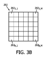
図3Bは、放射線感受性領域(2021,1、...、2021、M、...、202K、1、... 202K、M)のマトリクスを有する光センサ202を示す。この例では、各領域(2021,1、...、2021、M、...、202K、1、...、202K、M)は、所定の関心エネルギーバンドのセットの1つに対応する。カプセル化材料114は、異なる量子ドット118を介して異なるエネルギーの入射X線光子204を吸収し、それを示す特性放射線を放出する。光センサ202の領域(2021,1、...、2021、M、...、202K、1、...、202K、M)は、対応する放出光を検出し、それを示す電気信号を生成する。電気信号は、本明細書で説明されるように、及び/又は他の方法で処理される前処理回路122にルーティングされる。
FIG. 3B shows an
図4は、2つの隣接するシンチレータ/フォトダイオード画素120を示す。この実施形態では、シンチレータ/フォトダイオード画素120のQDシンチレータの間のバリア402は、材料114の堆積又は形成プロセスに含まれることができる。ガドリニウムオキシサルファイド(GOS)、ガーネット、及び/又は他の剛性のシンチレータシンチレータで行われるような、シンチレータの形成後のバリアの後続するソーイングのための何れかの必要性を軽減する。一般に、バリア402は、シンチレータ/フォトダイオード画素120の間のクロストークを軽減するために反射性塗料で満たされ、対応するフォトセンサ202に光子を向けることができる。
FIG. 4 shows two adjacent scintillator /
図5及び図6を参照すると、画素120の材料114は、複数のQDシンチレーション層5001,5002、... 500L(Lは1より大きい整数)を含み、それぞれは同じ吸収及び放出特性を有する量子ドット1181、...、118Nのグループの1つを有する。光センサ200は、複数の光センサ2021,2022、...、202Lを含む。 QDシンチレーション層5001,5002、...、500Lの各々の一つは、フォトセンサ2021,2022、...、202Lの対応する1つに結合される。他の実施形態では、フォトセンサ2021,2022、...、202Lは、 QDシンチレーション層の下の代わりに、QDシンチレーション層の側面に結合される。そのような構成は、2009年10月29日に出願された「スペクトルイメージング検出器」と題する米国特許第9,00,382号に示される。一例として、カプセル化材料の薄いスライスが各層の間に配置される。他の例では、層は、その間に配置されるカプセル化材料の薄いスライスなしに結合される。一般に、これらの層は、入射X線が最も低いエネルギー層に最初に衝突し、最も高いエネルギー層に最後に衝突するように順序付けられる。この構成は、層が関心スペクトルバンド幅を実現するようにスタックされることができるという点でスケーラブルである。
Referring to FIGS. 5 and 6, the
図7及び図8を参照すると、光センサ202は、3次元の内部感光面又は壁を備える没入部702を含む。図示の例では、没入部702は、四角錐台形状を有する。本明細書では他の形状も考えられる。図8は、没入部702内に配置される材料114を備え、材料114は没入部702の形状に一致する、図7の光センサ202の断面図を示す。図8において、材料114は単一層であり、同じ吸収及び放出特性を有する複数の量子ドットを含む。この形状を有する光センサの一例が、2013年11月23日に出願された「イメージング検出器」と題する国際公開第2014/087295号公報に記載されており、その全体が参照により本明細書に組み込まれる。
With reference to FIGS. 7 and 8, the
図9は、マルチエネルギー(スペクトル)構成を提供する垂直構成でスタックされる複数の結合される直接変換要素9021,9022、...、902P(Pは整数)を備える画素120を示す。この例では、直接変換素子9021,9022、...、902Pのそれぞれは、孔内に量子ドット118を有する多孔質シリコンを含み、異なる直接変換素子9021,9022、...、902Pのための量子ドット118は、異なる吸収及び放出特性を有する。直接変換素子9021,9022、...、902Pは、没入部及び三次元検出面を有する図7の光センサ202と同様の形状である。
直接変換素子9021は、第1(最高)のエネルギーバンドに調整され、(読み出し)電極9041と電気的に接触している。直接変換素子9022は、異なるエネルギーバンドに調整され、(読み出し)電極9042と電気的に接触しており、ビア9061を通じて直接変換素子9021を通じて延在する。直接変換素子902pは、さらに他の(最も低い)エネルギーバンドに調整され、(読み出し)電極904pと電気的に接触しており、ビア9062を通じて直接変換素子9021及び9022を通じて延在する。図示の実施形態では、没入部は空である。他の実施形態では、没入部は充填材料で充填される。
図10は図8のデュアルエネルギ変化を示す。図10において、材料114は、絶縁分離層1000によって分離される光センサ領域2021及び2022にそれぞれ対応する層1141及び1142を含む。層1141及び1142は、異なる吸収及び放出特性を有し、領域2021及び2022は異なるスペクトル感度を有する。領域2021及び2022のそれぞれは、それ自身の読み出し電極10021及び10022を有し、電極10022は、ビア1004を介して、領域2022を通じて領域2021にルーティングされる。この形状を有するマルチエネルギー画素構成の例が、 「イメージング検出器」と題され、2013年11月23日に出願された国際公開第2014/087295号公報に記載され、その全体が参照により本明細書に組み込まれる。
図11は、直接変換画素として構成される材料114の一例を示す。図2と同様に、この実施形態では、量子ドットは、異なるエネルギーバンド幅に対応し、単一層を通じて分布される。図12は、個々の粒子116からの例示的な読み出しを示し、同じエネルギーバンド幅に対応する粒子の出力は同じ経路にルーティングされ、異なるエネルギーバンド幅の粒子は異なる経路にルーティングされる。
図13は、直接変換画素として構成される材料114の一例を示し、異なるエネルギーバンド幅に対応する量子ドットが異なる層に分布される。層の順序付けは、図5及び9及び/又は他に関連して説明されるものと同様になり得る。各層についての読み出しは、図9及び図12及び/又は他に関連して示され、説明されるものと同様になり得る。
Figure 9 is a direct conversion element 902 1, 902 2 are a plurality of bonds that are stacked in a vertical configuration to provide a multi-energy (spectrum) configuration, ..., (the integer P) of a
Direct conversion element 902 1 is adjusted to the energy band of the first (highest) and is in electrical contact 1 and the (read) electrode 904. Direct conversion element 902 2 is adjusted to different energy bands in electrical contact with (read) the electrode 904 2, extending through direct conversion device 902 1 through vias 906 1. The direct conversion element 902 p is tuned to yet another (lowest) energy band, is in electrical contact with the (read) electrode 904 p, and extends through the direct conversion elements 902 1 and 902 2 through the via 906 2. To do. In the illustrated embodiment, the immersive portion is empty. In another embodiment, the immersion part is filled with a filling material.
FIG. 10 shows the dual energy change of FIG. In FIG. 10, the
FIG. 11 shows an example of a material 114 configured as a direct conversion pixel. Similar to FIG. 2, in this embodiment, the quantum dots correspond to different energy bandwidths and are distributed through a single layer. FIG. 12 shows an exemplary readout from
FIG. 13 shows an example of the material 114 configured as a direct conversion pixel, in which quantum dots corresponding to different energy bandwidths are distributed in different layers. The ordering of the layers can be similar to that described in relation to FIGS. 5 and 9 and / or others. Readouts for each layer can be similar to those shown and described in connection with FIGS. 9 and 12 and / or others.
図11及び13に関して、カプセル化材料は多孔質シリコンを含み、量子ドット118がシリコンの細孔の少なくとも一部をその間の電子 - 正孔対で充填し、入射X線を電気信号に直接変換することを可能にする。多孔質シリコンに堆積される量子ドットは、直接変換に使用される他の材料と比較されるとき、材料と接触する増大する表面積及び増大される応答性のために非常に高いQEを備える低コストの直接変換X線検出器を可能にする。
PETに関して、代わりに粒子116は、ガンマ線バンド幅で吸収するシンチレーション材料を有する量子ドット118を含む。本明細書で説明されるように、単一の層又はスタック層が用いられることができる。一般に、より高いエネルギー放射線を吸収するために、PET用途のための材料114の厚さは、CT用途のための材料114の厚さの10倍オーダになり得る。
図14は、検出器アレイ112によるイメージングを示す。
以下の実行の順序付けは説明のためのものであり、限定するものではないことを理解される。このように、本明細書では他の順序も考えられる。さらに、一つ又はそれより多くの動作が省略されてもよく、及び/又は一つ又はそれより多くの他の動作が含まれてもよい。
1402において、透過X線放射線がX線管によって生成される。
1404において、透過放射線は検査視野を横断する。
1406において、検出器アレイ112は、検査視野を横断する透過放射線を検出する。本明細書で説明するように、検出器アレイ112は、量子ドット118を有する材料114を含む。
1408において、それを示す電気信号が生成される。
1410において、電気信号が処理されて、患者の一部分を含む検査視野の画像が生成される。
図15は、検出器アレイ112によるイメージングを示す。
以下の実行の順序付けは説明のためのものであり、限定するものではないことを理解される。このように、本明細書では他の順序も考えられる。さらに、一つ又はそれより多くの動作が省略されてもよく、及び/又は一つ又はそれより多くの他の動作が含まれてもよい。
With respect to FIGS. 11 and 13, the encapsulation material contains porous silicon, where
For PET,
FIG. 14 shows imaging with the
It is understood that the following order of execution is for illustration purposes only and is not limiting. Thus, other sequences are conceivable herein. In addition, one or more actions may be omitted and / or one or more other actions may be included.
At 1402, transmitted X-ray radiation is produced by the X-ray tube.
At 1404, transmitted radiation crosses the field of view.
At 1406, the
At 1408, an electrical signal is generated to indicate this.
At 1410, the electrical signal is processed to produce an image of the examination field of view containing a portion of the patient.
FIG. 15 shows imaging with the
It is understood that the following order of execution is for illustration purposes only and is not limiting. Thus, other sequences are conceivable herein. In addition, one or more actions may be omitted and / or one or more other actions may be included.
1502において、ガンマ放射線が患者によって摂取される薬剤によって放出される。
1504において、放出放射線が検査視野を横断する。
1506において、検出器アレイ112は検査視野を横断する放出放射線を検出する。 本明細書で説明するように、検出器アレイ112は、量子ドット118を有する材料114を含む。
1508において、それを示す電気信号が生成される。
1510において、電気信号は、患者の一部分を含む検査視野の画像を生成するように処理される。
本発明は、様々な実施形態を参照して本明細書で説明される。 本明細書の説明を読むと、他の人に変更及び改変が生じる可能性がある。 本発明は、添付の特許請求の範囲又はその等価物の範囲内に入る限りにおいて、そのような改変及び変更の全てを含むと解釈されることが意図される。
At 1502, gamma radiation is emitted by the drug ingested by the patient.
At 1504, the emitted radiation crosses the field of view.
At 1506, the
At 1508, an electrical signal is generated to indicate this.
At 1510, the electrical signal is processed to produce an image of the examination field of view that includes a portion of the patient.
The present invention is described herein with reference to various embodiments. Reading the description herein may result in changes and alterations to others. The present invention is intended to be construed as including all such modifications and modifications, to the extent that it falls within the scope of the appended claims or its equivalents.
Claims (14)
放射線感受性検出器アレイであって、
一つ又はそれより多くの異なるシンチレーション材料をサポートする一つ又はそれより多くの粒子を備える光学的に透明なカプセル化材料を含み、各々の前記シンチレーション材料はナノメートル乃至マイクロメートルの量子ドットの形態であり、前記光学的に透明なカプセル化材料が、吸収される放射線を、前記吸収される放射線のエネルギーを示す電気信号に直接変換する直接変換材料を含み、前記直接変換材料内に前記一つ又はそれより多くの粒子を有する、
検出器画素
を含む、放射線感受性検出器アレイ
を有する、放射線検出システム。 It is a radiation detection system of an imaging system, and the radiation detection system is
Radiation sensitivity detector array
Each said scintillation material is in the form of nanometer to micrometer quantum dots, including an optically transparent encapsulating material with one or more particles supporting one or more different scintillation materials. der is, the optically transparent encapsulating material, the radiation absorbed, includes a direct conversion material for directly converting to an electrical signal indicative of the energy of radiation the absorption, the one in the direct conversion in the material Has one or more particles,
A radiation detection system having a radiation sensitivity detector array, including detector pixels.
を更に有する、請求項3に記載の放射線検出システム。 The radiation detection system of claim 3, further comprising a photosensor, wherein the single scintillation layer is coupled to the photosensor.
を更に有する、請求項2乃至5の何れか一項に記載の放射線検出システム。 The second detector pixel, the optically transparent encapsulating material of the detector pixel, and the optically transparent encapsulating material of the second detector pixel have a non-zero width. The radiation detection system according to any one of claims 2 to 5, further comprising a second detector pixel, separated by a material-free region.
を更に有する、請求項6に記載の放射線検出システム。 The radiation detection system according to claim 6, further comprising a reflective material arranged in the material-free region.
前記異なるシンチレーション材料の前記第二のシンチレーション材料に結合される第二の光センサと
を更に有する、請求項8に記載の放射線検出システム。 A first optical sensor coupled to the first scintillation material of the different scintillation material,
The radiation detection system according to claim 8, further comprising a second photosensor coupled to the second scintillation material of the different scintillation material.
を更に有する、請求項1に記載の放射線検出システム。 1. An optical sensor comprising an immersive portion and a three-dimensional photosensitive surface, wherein the optically transparent encapsulating material further comprises an optical sensor that is disposed within the immersive portion with respect to the three-dimensional photosensitive surface. The radiation detection system described in.
前記検出器画素で、前記受信される放射線を示す信号を生成するステップと、
前記信号を再構成して画像を構成するステップと
を有する、方法。 And receiving a radiation detector pixel, wherein the detector pixel involves encapsulating material comprising one or more quantum dots, each of the quantum dots seen including a scintillation material, the capsule The scintillation material comprises a direct conversion material that directly converts the absorbed radiation into an electrical signal indicating the energy of the absorbed radiation, and has one or more quantum dots in the direct conversion material. Steps and
In the detector pixel, a step of generating a signal indicating the received radiation, and
A method comprising reconstructing the signal to form an image.
前記カプセル化材料に結合される光センサの第一の領域で、前記少なくとも2つの量子ドットの第一の量子ドットに対応する第一の信号を生成するステップと、
前記光センサの第二の領域で、前記少なくとも2つの量子ドットの第二の量子ドットに対応する第二の信号を生成するステップと、
前記第一の信号を再構成して第一のスペクトル画像を構成し、前記第二の信号を再構成して第二のスペクトル画像を構成するステップと
を更に有する、請求項13に記載の方法。 At least two of the quantum dots contain different scintillation materials corresponding to different energy spectra, and the at least two quantum dots are all in the same layer of the encapsulation material.
A step of generating a first signal corresponding to the first quantum dot of the at least two quantum dots in the first region of the optical sensor coupled to the encapsulation material.
In the second region of the optical sensor, a step of generating a second signal corresponding to the second quantum dot of the at least two quantum dots,
13. The method of claim 13 , further comprising reconstructing the first signal to form a first spectral image and further reconstructing the second signal to form a second spectral image. ..
Applications Claiming Priority (3)
| Application Number | Priority Date | Filing Date | Title |
|---|---|---|---|
| US201562202397P | 2015-08-07 | 2015-08-07 | |
| US62/202,397 | 2015-08-07 | ||
| PCT/IB2016/054767 WO2017025888A1 (en) | 2015-08-07 | 2016-08-08 | Quantum dot based imaging detector |
Publications (3)
| Publication Number | Publication Date |
|---|---|
| JP2018529083A JP2018529083A (en) | 2018-10-04 |
| JP2018529083A5 JP2018529083A5 (en) | 2019-09-19 |
| JP6876033B2 true JP6876033B2 (en) | 2021-05-26 |
Family
ID=56852303
Family Applications (1)
| Application Number | Title | Priority Date | Filing Date |
|---|---|---|---|
| JP2018505004A Active JP6876033B2 (en) | 2015-08-07 | 2016-08-08 | Quantum dot based imaging detector |
Country Status (5)
| Country | Link |
|---|---|
| US (1) | US10527739B2 (en) |
| EP (1) | EP3332268B1 (en) |
| JP (1) | JP6876033B2 (en) |
| CN (1) | CN107850676B (en) |
| WO (1) | WO2017025888A1 (en) |
Families Citing this family (22)
| Publication number | Priority date | Publication date | Assignee | Title |
|---|---|---|---|---|
| EP3332269B1 (en) | 2015-08-07 | 2020-09-09 | Koninklijke Philips N.V. | Hybrid pet / ct imaging detector |
| US11156727B2 (en) * | 2015-10-02 | 2021-10-26 | Varian Medical Systems, Inc. | High DQE imaging device |
| CN108885273B (en) | 2016-03-23 | 2023-09-08 | 皇家飞利浦有限公司 | Nanomaterial imaging detector with integral pixel boundaries |
| CN109891269B (en) | 2016-10-26 | 2023-11-10 | 皇家飞利浦有限公司 | Radiation detector scintillator with integral via interconnect |
| EP3399344B1 (en) | 2017-05-03 | 2021-06-30 | ams International AG | Semiconductor device for indirect detection of electromagnetic radiation and method of production |
| KR20200083433A (en) | 2017-08-03 | 2020-07-08 | 더 리서치 파운데이션 포 더 스테이트 유니버시티 오브 뉴욕 | Dual-screen digital radiography with asymmetric reflective screen |
| WO2019144344A1 (en) | 2018-01-25 | 2019-08-01 | Shenzhen Xpectvision Technology Co., Ltd. | Radiation detector with quantum dot scintillator |
| EP3776006A1 (en) | 2018-03-29 | 2021-02-17 | Koninklijke Philips N.V. | Pixel definition in a porous silicon quantum dot radiation detector |
| WO2019185376A1 (en) * | 2018-03-29 | 2019-10-03 | Koninklijke Philips N.V. | Quantum dot x-ray radiation detector array with improved charge collection efficiency and/or detection efficiency |
| WO2019185846A1 (en) * | 2018-03-29 | 2019-10-03 | Koninklijke Philips N.V. | X-ray radiation detector with a porous silicon interposer |
| JP7330203B2 (en) * | 2018-03-30 | 2023-08-21 | コーニンクレッカ フィリップス エヌ ヴェ | Self-sufficient quantum dot radiation detector module |
| CA3080643C (en) | 2018-05-23 | 2021-06-15 | The Research Foundation For The State University Of New York | Flat panel x-ray imager with scintillating glass substrate |
| EP3618115A1 (en) * | 2018-08-27 | 2020-03-04 | Rijksuniversiteit Groningen | Imaging device based on colloidal quantum dots |
| EP3853637A1 (en) * | 2018-09-19 | 2021-07-28 | Sensinite Oy | An apparatus for detecting radiation |
| CN109471185A (en) * | 2018-12-17 | 2019-03-15 | 同方威视技术股份有限公司 | CT system and detection device for CT system |
| CN109782328B (en) | 2019-01-11 | 2021-03-26 | 惠科股份有限公司 | Radiation converter and radiation detection flat panel device |
| WO2020187769A1 (en) * | 2019-03-20 | 2020-09-24 | Koninklijke Philips N.V. | Pixelation for a quantum dot porous silicon membrane-based radiation detector |
| EP3942336B1 (en) | 2019-03-20 | 2022-12-28 | Koninklijke Philips N.V. | Quantum dot porous silicon membrane-based radiation detector |
| JP7196020B2 (en) * | 2019-06-14 | 2022-12-26 | キヤノン株式会社 | Radiation detection device and radiography system |
| EP3754382B1 (en) * | 2019-06-17 | 2023-10-25 | Detection Technology Oyj | Radiation detector and method for manufacturing thereof |
| WO2021016746A1 (en) | 2019-07-26 | 2021-02-04 | Shenzhen Xpectvision Technology Co., Ltd. | Radiation detector with quantum dot scintillators |
| EP4208739A1 (en) * | 2020-09-02 | 2023-07-12 | The Research Foundation for The State University of New York | Tapered scintillator crystal modules and methods of using the same |
Family Cites Families (21)
| Publication number | Priority date | Publication date | Assignee | Title |
|---|---|---|---|---|
| DE10058810A1 (en) * | 2000-11-27 | 2002-06-06 | Philips Corp Intellectual Pty | X-ray detector module |
| US20060015170A1 (en) * | 2004-07-16 | 2006-01-19 | Jones Ryan A | Contrast coated stent and method of fabrication |
| US7857993B2 (en) * | 2004-09-14 | 2010-12-28 | Ut-Battelle, Llc | Composite scintillators for detection of ionizing radiation |
| KR100594307B1 (en) * | 2004-12-24 | 2006-06-30 | 삼성전자주식회사 | Non-volatile memory with buried trench control gate and fabricating method the same |
| US20070085010A1 (en) | 2005-06-14 | 2007-04-19 | The Regents Of The University Of California | Scintillator with a matrix material body carrying nano-material scintillator media |
| US20080121806A1 (en) * | 2006-11-29 | 2008-05-29 | Ron Grazioso | Wavelength shifting lightguides for optimal photodetection in light-sharing applications |
| US7608829B2 (en) * | 2007-03-26 | 2009-10-27 | General Electric Company | Polymeric composite scintillators and method for making same |
| CN102838992A (en) * | 2007-03-26 | 2012-12-26 | 通用电气公司 | Scintillator and method for making same |
| US8338790B2 (en) | 2007-12-21 | 2012-12-25 | Koninklijke Philips Electronics N.V. | Radiation-sensitive detector with a scintillator in a composite resin |
| US8816287B2 (en) | 2008-01-14 | 2014-08-26 | Weinberg Medical Physics Llc | Structures for radiation detection and energy conversion using quantum dots |
| US8431041B2 (en) | 2008-03-31 | 2013-04-30 | Stc.Unm | Halide-based scintillator nanomaterial |
| EP2347284B1 (en) | 2008-11-18 | 2018-05-23 | Koninklijke Philips N.V. | Spectral imaging detector |
| US8614420B2 (en) * | 2010-01-07 | 2013-12-24 | Saint-Gobain Ceramics & Plastics, Inc. | Radiation detection system including a plurality of scintillators having different light yields and method of using the same |
| WO2011153280A2 (en) * | 2010-06-01 | 2011-12-08 | Saint-Gobain Ceramics & Plastics, Inc. | Radiation sensor to detect different targeted radiation and radiation detection system including the radiation sensor |
| US9422159B2 (en) | 2010-07-15 | 2016-08-23 | Leigh E. Colby | Quantum dot digital radiographic detection system |
| JP2012032170A (en) * | 2010-07-28 | 2012-02-16 | Fujifilm Corp | Radiation detector and method of manufacturing radiation detector |
| CN102628951B (en) * | 2012-03-30 | 2014-01-29 | 中国科学院合肥物质科学研究院 | Radiation dose measurement method based on quantum dot electroluminescent principle |
| JP6445978B2 (en) * | 2012-12-03 | 2018-12-26 | コーニンクレッカ フィリップス エヌ ヴェKoninklijke Philips N.V. | Imaging detector |
| JP6360150B2 (en) | 2013-03-20 | 2018-07-18 | コーニンクレッカ フィリップス エヌ ヴェKoninklijke Philips N.V. | Encapsulated quantum dots in porous particles |
| DE102013226365A1 (en) * | 2013-12-18 | 2015-06-18 | Siemens Aktiengesellschaft | Hybrid organic X-ray detector with conductive channels |
| US20170306221A1 (en) | 2014-09-23 | 2017-10-26 | Philips Lighting Holding B.V. | Encapsulated materials in porous particles |
-
2016
- 2016-08-08 CN CN201680046421.5A patent/CN107850676B/en active Active
- 2016-08-08 WO PCT/IB2016/054767 patent/WO2017025888A1/en active Application Filing
- 2016-08-08 EP EP16759868.9A patent/EP3332268B1/en active Active
- 2016-08-08 JP JP2018505004A patent/JP6876033B2/en active Active
- 2016-08-08 US US15/745,171 patent/US10527739B2/en active Active
Also Published As
| Publication number | Publication date |
|---|---|
| WO2017025888A1 (en) | 2017-02-16 |
| CN107850676B (en) | 2022-01-14 |
| EP3332268A1 (en) | 2018-06-13 |
| US20180203134A1 (en) | 2018-07-19 |
| CN107850676A (en) | 2018-03-27 |
| US10527739B2 (en) | 2020-01-07 |
| EP3332268B1 (en) | 2021-05-19 |
| JP2018529083A (en) | 2018-10-04 |
Similar Documents
| Publication | Publication Date | Title |
|---|---|---|
| JP6876033B2 (en) | Quantum dot based imaging detector | |
| US10509136B2 (en) | Detector systems for radiation imaging | |
| US10663606B2 (en) | Detector systems for integrated radiation imaging | |
| US10067239B2 (en) | Detector systems for radiation imaging | |
| CN108139491B (en) | Radiation detector for combined detection of low-energy and high-energy radiation quanta | |
| US20100012845A1 (en) | Energy-resolving detection system and imaging system | |
| JP6854805B2 (en) | Hybrid PET / CT imaging detector | |
| US7613274B2 (en) | Method and system of energy integrating and photon counting using layered photon counting detector | |
| JP6367969B2 (en) | Radiation detector having a photosensitive element capable of having a high aspect ratio | |
| CN109874343A (en) | Anti-scatter grid for radiation detector | |
| US20100282972A1 (en) | Indirect radiation detector | |
| JP2014510274A (en) | System, method and apparatus for imaging array using non-uniform partition walls | |
| JP7041633B2 (en) | Nanomaterial imaging detector with integrated pixel boundaries | |
| JP2019507335A (en) | Layered pixel detector for ionizing radiation | |
| Russo et al. | Solid-state detectors for small-animal imaging | |
| Llosá et al. | New Trends in Detectors for Medical Imaging |
Legal Events
| Date | Code | Title | Description |
|---|---|---|---|
| A521 | Request for written amendment filed |
Free format text: JAPANESE INTERMEDIATE CODE: A523 Effective date: 20190805 |
|
| A621 | Written request for application examination |
Free format text: JAPANESE INTERMEDIATE CODE: A621 Effective date: 20190805 |
|
| A977 | Report on retrieval |
Free format text: JAPANESE INTERMEDIATE CODE: A971007 Effective date: 20200626 |
|
| A131 | Notification of reasons for refusal |
Free format text: JAPANESE INTERMEDIATE CODE: A131 Effective date: 20200714 |
|
| A601 | Written request for extension of time |
Free format text: JAPANESE INTERMEDIATE CODE: A601 Effective date: 20201013 |
|
| A521 | Request for written amendment filed |
Free format text: JAPANESE INTERMEDIATE CODE: A523 Effective date: 20210114 |
|
| TRDD | Decision of grant or rejection written | ||
| A01 | Written decision to grant a patent or to grant a registration (utility model) |
Free format text: JAPANESE INTERMEDIATE CODE: A01 Effective date: 20210408 |
|
| A61 | First payment of annual fees (during grant procedure) |
Free format text: JAPANESE INTERMEDIATE CODE: A61 Effective date: 20210423 |
|
| R150 | Certificate of patent or registration of utility model |
Ref document number: 6876033 Country of ref document: JP Free format text: JAPANESE INTERMEDIATE CODE: R150 |