EP3332268B1 - Quantum dot based imaging detector - Google Patents
Quantum dot based imaging detector Download PDFInfo
- Publication number
- EP3332268B1 EP3332268B1 EP16759868.9A EP16759868A EP3332268B1 EP 3332268 B1 EP3332268 B1 EP 3332268B1 EP 16759868 A EP16759868 A EP 16759868A EP 3332268 B1 EP3332268 B1 EP 3332268B1
- Authority
- EP
- European Patent Office
- Prior art keywords
- radiation
- different
- detection system
- photosensor
- radiation detection
- Prior art date
- Legal status (The legal status is an assumption and is not a legal conclusion. Google has not performed a legal analysis and makes no representation as to the accuracy of the status listed.)
- Active
Links
- 239000002096 quantum dot Substances 0.000 title claims description 37
- 238000003384 imaging method Methods 0.000 title claims description 18
- 239000000463 material Substances 0.000 claims description 81
- 230000005855 radiation Effects 0.000 claims description 55
- 239000010410 layer Substances 0.000 claims description 35
- 238000006243 chemical reaction Methods 0.000 claims description 27
- 239000002245 particle Substances 0.000 claims description 18
- 238000001514 detection method Methods 0.000 claims description 14
- 238000000034 method Methods 0.000 claims description 11
- 230000003595 spectral effect Effects 0.000 claims description 10
- 238000010521 absorption reaction Methods 0.000 claims description 6
- 239000002356 single layer Substances 0.000 claims description 6
- 230000035945 sensitivity Effects 0.000 claims description 5
- 239000011159 matrix material Substances 0.000 claims description 2
- 238000001228 spectrum Methods 0.000 claims description 2
- 238000002591 computed tomography Methods 0.000 description 10
- 239000011148 porous material Substances 0.000 description 6
- 238000002600 positron emission tomography Methods 0.000 description 6
- 230000008569 process Effects 0.000 description 6
- 230000004888 barrier function Effects 0.000 description 3
- 230000005540 biological transmission Effects 0.000 description 3
- 239000002131 composite material Substances 0.000 description 3
- 239000013078 crystal Substances 0.000 description 3
- 238000004519 manufacturing process Methods 0.000 description 3
- 230000003287 optical effect Effects 0.000 description 3
- 229910021426 porous silicon Inorganic materials 0.000 description 3
- 239000002243 precursor Substances 0.000 description 3
- MCVAAHQLXUXWLC-UHFFFAOYSA-N [O-2].[O-2].[S-2].[Gd+3].[Gd+3] Chemical compound [O-2].[O-2].[S-2].[Gd+3].[Gd+3] MCVAAHQLXUXWLC-UHFFFAOYSA-N 0.000 description 2
- 230000004075 alteration Effects 0.000 description 2
- 230000015572 biosynthetic process Effects 0.000 description 2
- QWUZMTJBRUASOW-UHFFFAOYSA-N cadmium tellanylidenezinc Chemical compound [Zn].[Cd].[Te] QWUZMTJBRUASOW-UHFFFAOYSA-N 0.000 description 2
- 230000009977 dual effect Effects 0.000 description 2
- 238000012986 modification Methods 0.000 description 2
- 230000004048 modification Effects 0.000 description 2
- 238000007781 pre-processing Methods 0.000 description 2
- 239000007787 solid Substances 0.000 description 2
- 241001465754 Metazoa Species 0.000 description 1
- XUIMIQQOPSSXEZ-UHFFFAOYSA-N Silicon Chemical compound [Si] XUIMIQQOPSSXEZ-UHFFFAOYSA-N 0.000 description 1
- 239000000853 adhesive Substances 0.000 description 1
- 230000001070 adhesive effect Effects 0.000 description 1
- 239000000919 ceramic Substances 0.000 description 1
- 238000000701 chemical imaging Methods 0.000 description 1
- 239000003795 chemical substances by application Substances 0.000 description 1
- 230000008878 coupling Effects 0.000 description 1
- 238000010168 coupling process Methods 0.000 description 1
- 238000005859 coupling reaction Methods 0.000 description 1
- 230000008021 deposition Effects 0.000 description 1
- 239000000945 filler Substances 0.000 description 1
- 239000002223 garnet Substances 0.000 description 1
- 230000000977 initiatory effect Effects 0.000 description 1
- 229910010272 inorganic material Inorganic materials 0.000 description 1
- 239000011147 inorganic material Substances 0.000 description 1
- 230000003993 interaction Effects 0.000 description 1
- 230000005865 ionizing radiation Effects 0.000 description 1
- 238000002955 isolation Methods 0.000 description 1
- 239000007788 liquid Substances 0.000 description 1
- 239000000203 mixture Substances 0.000 description 1
- 239000002105 nanoparticle Substances 0.000 description 1
- 239000003973 paint Substances 0.000 description 1
- 230000000379 polymerizing effect Effects 0.000 description 1
- 229910052710 silicon Inorganic materials 0.000 description 1
- 239000010703 silicon Substances 0.000 description 1
Images


Classifications
-
- G—PHYSICS
- G01—MEASURING; TESTING
- G01T—MEASUREMENT OF NUCLEAR OR X-RADIATION
- G01T1/00—Measuring X-radiation, gamma radiation, corpuscular radiation, or cosmic radiation
- G01T1/16—Measuring radiation intensity
- G01T1/20—Measuring radiation intensity with scintillation detectors
- G01T1/2018—Scintillation-photodiode combinations
- G01T1/20183—Arrangements for preventing or correcting crosstalk, e.g. optical or electrical arrangements for correcting crosstalk
-
- B—PERFORMING OPERATIONS; TRANSPORTING
- B82—NANOTECHNOLOGY
- B82Y—SPECIFIC USES OR APPLICATIONS OF NANOSTRUCTURES; MEASUREMENT OR ANALYSIS OF NANOSTRUCTURES; MANUFACTURE OR TREATMENT OF NANOSTRUCTURES
- B82Y15/00—Nanotechnology for interacting, sensing or actuating, e.g. quantum dots as markers in protein assays or molecular motors
-
- G—PHYSICS
- G01—MEASURING; TESTING
- G01T—MEASUREMENT OF NUCLEAR OR X-RADIATION
- G01T1/00—Measuring X-radiation, gamma radiation, corpuscular radiation, or cosmic radiation
- G01T1/16—Measuring radiation intensity
- G01T1/161—Applications in the field of nuclear medicine, e.g. in vivo counting
-
- G—PHYSICS
- G01—MEASURING; TESTING
- G01T—MEASUREMENT OF NUCLEAR OR X-RADIATION
- G01T1/00—Measuring X-radiation, gamma radiation, corpuscular radiation, or cosmic radiation
- G01T1/16—Measuring radiation intensity
- G01T1/20—Measuring radiation intensity with scintillation detectors
- G01T1/2018—Scintillation-photodiode combinations
- G01T1/20181—Stacked detectors, e.g. for measuring energy and positional information
-
- G—PHYSICS
- G01—MEASURING; TESTING
- G01T—MEASUREMENT OF NUCLEAR OR X-RADIATION
- G01T1/00—Measuring X-radiation, gamma radiation, corpuscular radiation, or cosmic radiation
- G01T1/16—Measuring radiation intensity
- G01T1/20—Measuring radiation intensity with scintillation detectors
- G01T1/2018—Scintillation-photodiode combinations
- G01T1/20185—Coupling means between the photodiode and the scintillator, e.g. optical couplings using adhesives with wavelength-shifting fibres
-
- G—PHYSICS
- G01—MEASURING; TESTING
- G01T—MEASUREMENT OF NUCLEAR OR X-RADIATION
- G01T1/00—Measuring X-radiation, gamma radiation, corpuscular radiation, or cosmic radiation
- G01T1/16—Measuring radiation intensity
- G01T1/20—Measuring radiation intensity with scintillation detectors
- G01T1/2018—Scintillation-photodiode combinations
- G01T1/20187—Position of the scintillator with respect to the photodiode, e.g. photodiode surrounding the crystal, the crystal surrounding the photodiode, shape or size of the scintillator
Definitions
- CT computed tomography
- PET positron emission tomography
- Computed tomography detection systems have employed scintillation/photodiode (indirect conversion) detectors. With these detectors, X-ray radiation incident on a scintillator are absorbed by scintillating material thereof, which in turn emits light photons that are detected by a photodiode, which in turn generates a signal indicative thereof.
- the scintillating material has included full size crystals, ceramics, or garnets. Unfortunately, these structures are generally rigid structures, limiting their shape. These structures are also relatively expensive.
- Energy discrimination is achieved through stacking layers of different scintillation materials, which absorb in different energy bandwidths of the X-ray radiation.
- the stack in general, goes from lower energy absorbing layers closer to the incident X-ray radiation to higher energy absorbing layers nearer to the photodiode.
- each additional layer increases the thickness of the detector and the amount of scintillating material and requires a photodiode. Unfortunately, this increases the overall cost of the detector and, hence, the CT scanner.
- Direct conversion detectors include a direct conversion material that directly converts incident X-ray radiation to electrical signals indicative of the energy of the X-ray radiation.
- An example of a direct conversion material is Cadmium Zinc Telluride (CZT).
- CZT Cadmium Zinc Telluride
- present day direct conversion materials are expensive and made from a solid crystal such that their shape is rigidly bound to the crystalline structure of the chosen medium. Furthermore, it takes time to grow the crystal, which adds cost to the manufacturing of the direct conversion detector.
- US patent application US2006/054863A discloses a composite scintillator having enhanced transparency for detecting ionizing radiation comprising a material having optical transparency wherein said material comprises nano-sized objects having a size in at least one dimension that is less than the wavelength of light emitted by said composite scintillator wherein said composite scintillator designed to have selected properties suitable for a particular application.
- the invention may take form in various components and arrangements of components, and in various steps and arrangements of steps.
- the drawings are only for illustrating purposes and are not to be construed as limiting the invention.
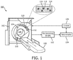
- FIGURE 1 schematically illustrates an example imaging system 100 such as a computed tomography (CT) system.
- CT computed tomography
- the imaging system 100 could alternatively be a positron emission tomography (PET) system, an X-ray system, a hybrid CT/PET system, a hybrid CT/MR (magnetic resonance) system, a hybrid PET/MR system, and/or other imaging system configured to detect radiation in in one or more energy bands and indirectly or directly convert the detected radiation to an electrical signal indicative thereof.
- PET positron emission tomography
- X-ray X-ray
- hybrid CT/PET hybrid CT/MR (magnetic resonance) system
- hybrid PET/MR magnetic resonance
- the imaging system 100 includes a generally stationary gantry 102 and a rotating gantry 104, which is rotatably supported by the stationary gantry 102.
- the rotating gantry 104 rotates around an examination region 106 about a longitudinal or z-axis.
- a subject support 108 such as a couch supports a human or animal patient or an object in the examination region 106.
- the subject support 108 is movable in coordination with scanning so as to guide the subject or object with respect to the examination region 106 for performing a scan of the subject or object.
- a radiation source 110 such as an x-ray tube, is supported by the rotating gantry 104 and emits poly-energetic/chromatic radiation.
- a radiation sensitive detector array 112 includes a plurality of detector pixels 120 that detect X-ray radiation traversing the examination region 106.
- the radiation sensitive detector array 112 may include one or more rows of the detector pixels 120 arranged with respect to each other along the z-axis direction.
- the radiation sensitive detector array 112 includes an indirect conversion based pixel 120 with a scintillation material that receives X-ray radiation and converts the X-ray radiation to light, and a corresponding photosensor that senses the light and generates an electrical signal indicative of the received radiation.
- the radiation sensitive detector array 112 includes a direct conversion based pixel 120 that receives X-ray radiation and directly converts the X-ray radiation to the electrical signal.
- the scintillation and/or direct conversion material includes an optically transparent and non-insulating encapsulate material 114 with one or more porous particles 116, which support one or more different scintillation materials 118 in the form of nanometer to micrometer quantum dots, embedded therein.
- Different groups of the different quantum dots 118 are encapsulated in the same layer of the material 114 (e.g., as shown) or in different layers (e.g., FIGURE 5 , etc.) of the material 114.
- the quantum dots 118 can be tuned (e.g., via density, thickness, type of scintillation material, etc.) to absorb in different energy bandwidths (e.g., 20keV to 140keV) and generate characteristic radiation and/or electrical signals.
- the detector array 112 described herein is well-suited for CT energy discrimination, without having to increase the amount of scintillation material and/or the photosensitive area, and the cost of the detector and/or scanner.
- the encapsulate material 114 is melted, e.g., by applying heat and the quantum dots 180 are mixed into the melted encapsulate material 114.
- the resulting mixture is formed into a predetermined number of layers of interest (e.g., one or more).
- Each layer may conform to a predetermined shape of interest (a polyhedron, a sphere, a spheroid, a cylinder, etc.) of a rigid structure or a shape independent of any rigid structure as the small diameter quantum dots 118 render an amorphous or non-crystalline solid.
- the latter may allow for reduced production cost and time, and increasing detective quantum efficiency and/or spectral discrimination.
- An example of the particle 116 is described in application serial number EP 14186022.1 , entitled “Encapsulated materials in porous particles," and filed on September 23, 2014.
- Pre-processing circuitry 122 processes the signal from the detector array 112.
- the detector array 112 is a scintillator/photodiode based detector array
- a pulse shaper processes the signal (which can first be amplified) and generates a pulse (e.g., voltage, current, etc.) having a height indicative of the energy of the detected radiation.
- the detector array 112 includes a direct conversion detector material, each pixel directly generates and outputs the pulse.
- a counter increments a count value for each threshold based on the output of the energy discriminator.
- a reconstructor 124 is configured to selectively reconstruct the detected signals.
- the reconstructor 124 reconstructs signals for a particular energy range.
- the reconstructor 124 can reconstructs signals one or more energies or energy ranges in the diagnostic range of 20keV to 140keV.
- the reconstructor combines the signals for all of the bins and reconstructs the combined signal to generate a conventional image over the energy spectrum of the emitted radiation.
- An operator console 126 includes a human readable output device such as a monitor or display and an input device such as a keyboard and mouse. Software resident on the console 126 allows the operator to interact with the scanner 100 via a graphical user interface (GUI) or otherwise. This interaction may include selecting a type of scan, selecting an imaging protocol, initiating scanning, etc.
- GUI graphical user interface
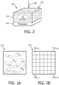
- FIGURES 2-10 illustrate an example of a scintillator/photodiode pixel 120. It is to be understood that the illustrated geometries and quantum dot density and size are for explanatory purposes and are not limiting.
- the material 114 is a single cube shaped block of scintillation material 114 ("QD SCINTILLATOR").
- the particles 116 and hence the quantum dots 118 are distributed homogeneously in the single cube shaped block of scintillation material 114.
- FIGURE 3A shows a top down view with quantum dots 118 1 , 118 2 , ..., 118 N (where N is an integer greater than one) distributed homogeneously therein.
- the block of material 114 is optically coupled to a photosensor 202.
- the optical coupling may include an optical adhesive.
- a reflective material may be disposed on and/or next to the other sides to direct light photons traversing away from the photosensor 202 to the photosensor 202.
- FIGURE 3B shows the photosensor 202 with a matrix of radiation sensitive regions (202 1,1, ..., 202 1,M , ..., 202 K,1, ... 202 K,M ).
- each of the regions (202 1,1, ..., 202 1,M, ..., 202 K,1, ... 202 K,M ) corresponds to one of a set of predetermined energy bands of interest.
- the encapsulate material 114 absorbs incident X-ray photons 204 of different energy via the different quantum dots 118 and emits characteristic radiation indicative thereof.
- the regions (202 1,1, ..., 202 1,M, ..., 202 K,1, ... 202 K,M ) of the photosensor 202 sense corresponding emitted light and generate electrical signal indicative thereof.
- the electrical signals are routed to the pre-processing circuitry 122, which processes as described herein and/or otherwise.
- FIGURE 4 shows two adjacent scintillator/photodiode pixels 120.
- a barrier 402 between the QD scintillators of scintillator /photodiode pixels 120 can be included in the deposition or formation process of the material 114. This mitigates any need for subsequently sawing of such a barrier after the formation of the scintillator, e.g., as done with gadolinium oxysulfide (GOS), garnet, and/or other rigid scintillator scintillators.
- the barrier 402 can be filled with a reflective paint to mitigate cross-talk between the scintillator/photodiode pixels 120 and direct light photons to the corresponding photosenors 202.
- the material 114 of the pixel 120 includes a plurality of QD scintillation layers 500 1 , 500 2 , ..., 500 L (where L is an integer greater than one), each with one of the groups of quantum dots 118 1 , ..., 118 N having the same absorption and emission characteristics.
- the photosensor 200 includes a plurality of photosensor 202 1 , 202 2 , ..., 202 L .
- Each one of the QD scintillation layers 500 1 , 500 2 , ..., 500 L is coupled to a corresponding one of the photosensors 202 1 , 202 2 , ..., 202 L
- the photosensors 202 1 , 202 2 , ..., 202 L as coupled at a side of the QD scintillation layers instead of below the QD scintillation layers.
- Such a configuration is shown in US 9,00,382 , entitled “Spectral Imaging Detector,” and filed on October 29, 2009.
- a thin slice of encapsulating material is disposed between each layer.
- the layers are coupled without the thin slice of encapsulating material disposed therebetween.
- the layers are ordered such that the incident X-rays strike the lowest energy layer first and the highest energy layer last. This configuration is scalable in that layers can be stack to achieve a spectral bandwidth of interest.
- the photosensor 202 includes a recess 702 with a three-dimensional inner photosensitive surface or walls.
- the recess 702 has a square frustum shape. Other shapes are also contemplated herein.
- FIGURE 8 shows cross-sectional view of the photosensor 202 of FIGURE 7 with the material 114 disposed in the recess 702, where the material 114, conforms to the shape of the recess 702.
- the material 114 is a single layer and includes a plurality of quantum dots with the same absorption and emission characteristics.
- An example of a photosensor having this shape is described in Publication WO 2014/087295 A1 , entitled “Imaging Detector,” and filed on November 23, 2013.
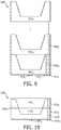
- FIGURE 9 illustrates a pixel 120 with a plurality of bonded direct conversion elements 902 1 , 902 2 , ..., 902p (where P is an integer) stacked in a vertical configuration, providing a multi-energy (spectral) configuration.
- each of the direct conversion elements 902 1 , 902 2 , ..., 902p includes a porous silicon with the quantum dots 118 in the pores, where the quantum dots 118 for the different direct conversion elements 902 1 , 902 2 , ..., 902p have different absorption and emission characteristics.
- the direct conversion elements 902 1 , 902 2 , ..., 902 P are shaped similar to the photosensor 202 of FIGURE 7 with a recess and a three-dimensional sensing surface.
- the direct conversion element 902 1 is tuned to a first (highest) energy band and is in electrical contact with an (read out) electrode 904 1 .
- the direct conversion element 902 2 is tuned to a different energy band and is in electrical contact with an (read out) electrode 904 2 , which extends through the direct conversion element 902 1 through a via 906 1 .
- the direct conversion element 902 p is tuned to yet another (lowest) energy band and is in electrical contact with an (read out) electrode 904 p , which extends through the direct conversion elements 902 1 and 902 2 through a via 906 2 .
- the recess is empty. In another embodiment, the recess is filled with a filler material.
- FIGURE 10 illustrates a dual energy variation of FIGURE 8 .
- the material 114 includes layers 114 1 and 114 2 , respectively corresponding to photosensor regions 202 1 and 202 2 which are separated by an isolation layer 1000.
- the layers 114 1 and 114 2 include quantum dots having different absorption and emission characteristics, and the regions 202 1 and 202 2 have different spectral sensitivities.
- Each of the regions 202 1 and 202 2 has its own read out electrical electrodes 1002 1 and 1002 2 , where the electrode 1002 2 is routed through the region 202 2 to the region 202 1 through a via 1004.
- An example of a multi energy pixel configuration with this shape is described in Publication WO 2014/087295 A1 , entitled “Imaging Detector,” and filed on November 23, 2013.
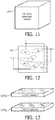
- FIGURE 11 illustrates an example of the material 114 configured as a direct conversion pixel. Similar to FIGURE 2 , in this embodiment quantum dots corresponding to different energy bandwidths and distributed throughout a single layer.
- FIGURE 12 shows exemplary read out from the individual particles 116, in which the output of particles corresponding to the same energy bandwidth are routed to the same path, with particles for different energy bandwidth routed to different paths.
- FIGURE 13 illustrates an example of the material 114 configured as a direct conversion pixel where the quantum dots corresponding to different energy bandwidths are distributed in different layers.
- the ordering of the layers can be similar to that described in connection with FIGURES 5 and 9 and/or otherwise. Read out for each layer can be similar to that shown and described in connection with FIGURES 9 and 12 and/or otherwise.
- the encapsulate material includes porous silicon
- the quantum dots 118 fill at least a portion of the pores of the silicon, electron-hole pairs therebetween, allowing for direct conversion of incident X-rays to the electrical signals.
- Quantum dots deposited in porous silicon enables a low cost direct conversion X-ray detector with very high QE due to increased surface area contact with the materials and increased responsivity when compared to other materials used for direct converters.
- the particles 116 instead include quantum dots 118 with a scintillation material that absorbs in the gamma radiation bandwidth.
- a single layer or stacked layers can be employed, as described herein.
- a thickness of the material 114 for a PET application may be on the order of ten times a thickness of a material 114 for a CT application to absorb the higher energy radiation.
- FIGURE 14 illustrates imaging with the detector array 112.
- transmission X-ray radiation is generated by an X-ray tube.
- the transmission radiation traverses an examination field of view.
- the detector array 112 detects the transmission radiation traversing the examination field of view. As described herein, the detector array 112 includes the material 114 with the quantum dots 118.
- the electrical signal is processed to generate an image of the examination field of view, including a portion of the patient therein.
- FIGURE 15 illustrates imaging with the detector array 112.
- gamma radiation is emitted by an agent ingested by a patient.
- the emission radiation traverses an examination field of view.
- the detector array 112 detects the emission radiation traversing the examination field of view.
- the detector array 112 includes the material 114 with the quantum dots 118.
- the electrical signal is processed to generate an image of the examination field of view, including a portion of the patient therein.
Landscapes
- Health & Medical Sciences (AREA)
- Physics & Mathematics (AREA)
- Life Sciences & Earth Sciences (AREA)
- Molecular Biology (AREA)
- Spectroscopy & Molecular Physics (AREA)
- High Energy & Nuclear Physics (AREA)
- General Physics & Mathematics (AREA)
- Chemical & Material Sciences (AREA)
- Engineering & Computer Science (AREA)
- Crystallography & Structural Chemistry (AREA)
- General Health & Medical Sciences (AREA)
- Nanotechnology (AREA)
- Biomedical Technology (AREA)
- Medical Informatics (AREA)
- Optics & Photonics (AREA)
- Nuclear Medicine, Radiotherapy & Molecular Imaging (AREA)
- Measurement Of Radiation (AREA)
- Apparatus For Radiation Diagnosis (AREA)
- Nuclear Medicine (AREA)
Description
- The following generally relates to an imaging detector and more particularly to a quantum dot based imaging detector, and is described with particular application to computed tomography (CT); however, the following is also amenable to other imaging modalities such as positron emission tomography (PET).
- Computed tomography detection systems have employed scintillation/photodiode (indirect conversion) detectors. With these detectors, X-ray radiation incident on a scintillator are absorbed by scintillating material thereof, which in turn emits light photons that are detected by a photodiode, which in turn generates a signal indicative thereof. The scintillating material has included full size crystals, ceramics, or garnets. Unfortunately, these structures are generally rigid structures, limiting their shape. These structures are also relatively expensive.
- Energy discrimination is achieved through stacking layers of different scintillation materials, which absorb in different energy bandwidths of the X-ray radiation. The stack, in general, goes from lower energy absorbing layers closer to the incident X-ray radiation to higher energy absorbing layers nearer to the photodiode. However, each additional layer increases the thickness of the detector and the amount of scintillating material and requires a photodiode. Unfortunately, this increases the overall cost of the detector and, hence, the CT scanner.
- Direct conversion detectors include a direct conversion material that directly converts incident X-ray radiation to electrical signals indicative of the energy of the X-ray radiation. An example of a direct conversion material is Cadmium Zinc Telluride (CZT). Unfortunately, present day direct conversion materials are expensive and made from a solid crystal such that their shape is rigidly bound to the crystalline structure of the chosen medium. Furthermore, it takes time to grow the crystal, which adds cost to the manufacturing of the direct conversion detector.
- International patent application
WO2014/147570 discloses a process for the production of a (particulate) luminescent material comprising particles which are at least partly filled with a polymeric material with luminescent quantum dots embedded therein, wherein the process comprises (i) impregnating the particles of a particulate porous inorganic material with pores with a first liquid ("ink") comprising the luminescent quantum dots and a curable or polymerizable precursor of the polymeric material, to provide pores that are at least partly filled with said luminescent quantum dots and curable or polymerizable precursor; and (ii) curing or polymerizing the curable or polymerizable precursor within pores of the porous material, as well as a product obtainable thereby. - US patent application
US2006/054863A discloses a composite scintillator having enhanced transparency for detecting ionizing radiation comprising a material having optical transparency wherein said material comprises nano-sized objects having a size in at least one dimension that is less than the wavelength of light emitted by said composite scintillator wherein said composite scintillator designed to have selected properties suitable for a particular application. - In view of at least the above, there is an unresolved need for another detector configuration.
- Aspects of the present application address the above-referenced matters and others.
- According to one aspect of the invention, there is a radiation detection system as defined in
independent claim 1. - In another aspect of the invention, there is a method as defined in independent claim 13.
- Still further aspects of the present invention will be appreciated to those of ordinary skill in the art upon reading and understand the following detailed description.
- The invention may take form in various components and arrangements of components, and in various steps and arrangements of steps. The drawings are only for illustrating purposes and are not to be construed as limiting the invention.
-
FIGURE 1 schematically illustrates an example imaging system with a quantum dot based imaging detector array. -
FIGURE 2 schematically illustrates an example of a pixel of the quantum dot based imaging detector for a scintillator/photosensor configuration with a single scintillation layer. -
FIGURE 3A schematically illustrates a top down view into the single scintillation layer ofFIGURE 2 . -
FIGURE 3B schematically illustrates a top down view into the photosensor ofFIGURE 2 . -
FIGURE 4 schematically illustrates two adjacent scintillator/photosensor pixels formed with spacing therebetween. -
FIGURE 5 schematically illustrates an example of a pixel of the quantum dot based imaging detector for a scintillator/photosensor configuration with multiple scintillation layers. -
FIGURE 6 schematically illustrates example scintillation layers of the configuration ofFIGURE 5 . -
FIGURE 7 schematically illustrates a pixel with a photosensor with a three dimensional photosensing surface. -
FIGURE 8 schematically illustrates a cross-sectional view of the configuration ofFIGURE 7 with a single scintillation layer including quantum dots. -
FIGURE 9 schematically illustrates a variation ofFIGURE 7 with stacked pixels forming a multi-energy configuration. -
FIGURE 10 schematically illustrates a variation ofFIGURE 8 for a dual energy configuration with two scintillation layers. -
FIGURE 11 schematically illustrates an example of a single block pixel for a direct conversion configuration according to an embodiment of the invention. -
FIGURE 12 schematically illustrates an example of routing signals from the quantum dot ofFIGURE 11 . -
FIGURE 13 schematically illustrates an example of a multiple layer pixel for a direct conversion configuration according to an embodiment of the invention. -
FIGURE 14 illustrates an example method in accordance with an embodiment of the invention. -
FIGURE 15 illustrates another example method in accordance with an embodiment of the invention. -
FIGURE 1 schematically illustrates anexample imaging system 100 such as a computed tomography (CT) system. However, it is to be understood that theimaging system 100 could alternatively be a positron emission tomography (PET) system, an X-ray system, a hybrid CT/PET system, a hybrid CT/MR (magnetic resonance) system, a hybrid PET/MR system, and/or other imaging system configured to detect radiation in in one or more energy bands and indirectly or directly convert the detected radiation to an electrical signal indicative thereof. - The
imaging system 100 includes a generallystationary gantry 102 and arotating gantry 104, which is rotatably supported by thestationary gantry 102. Therotating gantry 104 rotates around anexamination region 106 about a longitudinal or z-axis. Asubject support 108 such as a couch supports a human or animal patient or an object in theexamination region 106. Thesubject support 108 is movable in coordination with scanning so as to guide the subject or object with respect to theexamination region 106 for performing a scan of the subject or object. Aradiation source 110, such as an x-ray tube, is supported by therotating gantry 104 and emits poly-energetic/chromatic radiation. - A radiation
sensitive detector array 112 includes a plurality ofdetector pixels 120 that detect X-ray radiation traversing theexamination region 106. The radiationsensitive detector array 112 may include one or more rows of thedetector pixels 120 arranged with respect to each other along the z-axis direction. In one instance, the radiationsensitive detector array 112 includes an indirect conversion basedpixel 120 with a scintillation material that receives X-ray radiation and converts the X-ray radiation to light, and a corresponding photosensor that senses the light and generates an electrical signal indicative of the received radiation. In another instance, the radiationsensitive detector array 112 includes a direct conversion basedpixel 120 that receives X-ray radiation and directly converts the X-ray radiation to the electrical signal. - The scintillation and/or direct conversion material includes an optically transparent and
non-insulating encapsulate material 114 with one or moreporous particles 116, which support one or moredifferent scintillation materials 118 in the form of nanometer to micrometer quantum dots, embedded therein. Different groups of the differentquantum dots 118 are encapsulated in the same layer of the material 114 (e.g., as shown) or in different layers (e.g.,FIGURE 5 , etc.) of thematerial 114. Thequantum dots 118 can be tuned (e.g., via density, thickness, type of scintillation material, etc.) to absorb in different energy bandwidths (e.g., 20keV to 140keV) and generate characteristic radiation and/or electrical signals. As such, thedetector array 112 described herein is well-suited for CT energy discrimination, without having to increase the amount of scintillation material and/or the photosensitive area, and the cost of the detector and/or scanner. - In one non-limiting instance, the
encapsulate material 114 is melted, e.g., by applying heat and the quantum dots 180 are mixed into the meltedencapsulate material 114. The resulting mixture is formed into a predetermined number of layers of interest (e.g., one or more). Each layer may conform to a predetermined shape of interest (a polyhedron, a sphere, a spheroid, a cylinder, etc.) of a rigid structure or a shape independent of any rigid structure as the small diameterquantum dots 118 render an amorphous or non-crystalline solid. The latter may allow for reduced production cost and time, and increasing detective quantum efficiency and/or spectral discrimination. An example of theparticle 116 is described in application serial numberEP 14186022.1 - Pre-processing
circuitry 122 processes the signal from thedetector array 112. For example, where thedetector array 112 is a scintillator/photodiode based detector array a pulse shaper processes the signal (which can first be amplified) and generates a pulse (e.g., voltage, current, etc.) having a height indicative of the energy of the detected radiation. Where thedetector array 112 includes a direct conversion detector material, each pixel directly generates and outputs the pulse. In either case, an energy discriminator energy-discriminates the pulse through, e.g., one or more comparators, each having a different energy threshold, which correspond to an energy of interest. A counter increments a count value for each threshold based on the output of the energy discriminator. A binner energy-bins the signals and, hence, the radiation, into two or more energy bins based on the counts, wherein an energy bin encompasses an energy window. - A
reconstructor 124 is configured to selectively reconstruct the detected signals. In one instance, thereconstructor 124 reconstructs signals for a particular energy range. For instance, thereconstructor 124 can reconstructs signals one or more energies or energy ranges in the diagnostic range of 20keV to 140keV. In another instance, the reconstructor combines the signals for all of the bins and reconstructs the combined signal to generate a conventional image over the energy spectrum of the emitted radiation. Anoperator console 126 includes a human readable output device such as a monitor or display and an input device such as a keyboard and mouse. Software resident on theconsole 126 allows the operator to interact with thescanner 100 via a graphical user interface (GUI) or otherwise. This interaction may include selecting a type of scan, selecting an imaging protocol, initiating scanning, etc. -
FIGURES 2-10 illustrate an example of a scintillator/photodiode pixel 120. It is to be understood that the illustrated geometries and quantum dot density and size are for explanatory purposes and are not limiting. - In
FIGURE 2 , thematerial 114 is a single cube shaped block of scintillation material 114 ("QD SCINTILLATOR"). In this example, theparticles 116 and hence the quantum dots 118 (shown as black dots inFIGURE 2 ) are distributed homogeneously in the single cube shaped block ofscintillation material 114.FIGURE 3A shows a top down view withquantum dots FIGURE 2 , the block ofmaterial 114 is optically coupled to aphotosensor 202. The optical coupling may include an optical adhesive. A reflective material may be disposed on and/or next to the other sides to direct light photons traversing away from the photosensor 202 to thephotosensor 202. -
FIGURE 3B shows the photosensor 202 with a matrix of radiation sensitive regions (2021,1, ..., 2021,M, ..., 202K,1, ... 202K,M). In this example, each of the regions (2021,1, ..., 2021,M, ..., 202K,1, ... 202K,M) corresponds to one of a set of predetermined energy bands of interest. Theencapsulate material 114 absorbsincident X-ray photons 204 of different energy via the differentquantum dots 118 and emits characteristic radiation indicative thereof. The regions (2021,1, ..., 2021,M, ..., 202K,1, ... 202K,M) of the photosensor 202 sense corresponding emitted light and generate electrical signal indicative thereof. The electrical signals are routed to thepre-processing circuitry 122, which processes as described herein and/or otherwise. -
FIGURE 4 shows two adjacent scintillator/photodiode pixels 120. In this exemplary arrangement, abarrier 402 between the QD scintillators of scintillator /photodiode pixels 120 can be included in the deposition or formation process of thematerial 114. This mitigates any need for subsequently sawing of such a barrier after the formation of the scintillator, e.g., as done with gadolinium oxysulfide (GOS), garnet, and/or other rigid scintillator scintillators. In general, thebarrier 402 can be filled with a reflective paint to mitigate cross-talk between the scintillator/photodiode pixels 120 and direct light photons to thecorresponding photosenors 202. - Turning to
FIGURES 5 and6 , thematerial 114 of thepixel 120 includes a plurality of QD scintillation layers 5001, 5002, ..., 500L (where L is an integer greater than one), each with one of the groups ofquantum dots 1181, ..., 118N having the same absorption and emission characteristics. The photosensor 200 includes a plurality ofphotosensor photosensors photosensors US 9,00,382 , entitled "Spectral Imaging Detector," and filed on October 29, 2009. In one instance, a thin slice of encapsulating material is disposed between each layer. In another instance, the layers are coupled without the thin slice of encapsulating material disposed therebetween. In general, the layers are ordered such that the incident X-rays strike the lowest energy layer first and the highest energy layer last. This configuration is scalable in that layers can be stack to achieve a spectral bandwidth of interest. - Turning to
FIGURES 7 and 8 , thephotosensor 202 includes arecess 702 with a three-dimensional inner photosensitive surface or walls. In the illustrated example, therecess 702 has a square frustum shape. Other shapes are also contemplated herein.FIGURE 8 shows cross-sectional view of thephotosensor 202 ofFIGURE 7 with the material 114 disposed in therecess 702, where thematerial 114, conforms to the shape of therecess 702. InFIGURE 8 , thematerial 114 is a single layer and includes a plurality of quantum dots with the same absorption and emission characteristics. An example of a photosensor having this shape is described in PublicationWO 2014/087295 A1 , entitled "Imaging Detector," and filed on November 23, 2013. -
FIGURE 9 illustrates apixel 120 with a plurality of bonded direct conversion elements 9021, 9022, ..., 902p (where P is an integer) stacked in a vertical configuration, providing a multi-energy (spectral) configuration. In this example, each of the direct conversion elements 9021, 9022, ..., 902p includes a porous silicon with thequantum dots 118 in the pores, where thequantum dots 118 for the different direct conversion elements 9021, 9022, ..., 902p have different absorption and emission characteristics. The direct conversion elements 9021, 9022, ..., 902P are shaped similar to thephotosensor 202 ofFIGURE 7 with a recess and a three-dimensional sensing surface. - The direct conversion element 9021 is tuned to a first (highest) energy band and is in electrical contact with an (read out) electrode 9041. The direct conversion element 9022 is tuned to a different energy band and is in electrical contact with an (read out) electrode 9042, which extends through the direct conversion element 9021 through a via 9061. The direct conversion element 902p is tuned to yet another (lowest) energy band and is in electrical contact with an (read out) electrode 904p, which extends through the direct conversion elements 9021 and 9022 through a via 9062. In the illustrated embodiment, the recess is empty. In another embodiment, the recess is filled with a filler material.
-
FIGURE 10 illustrates a dual energy variation ofFIGURE 8 . InFIGURE 10 , thematerial 114 includeslayers photosensor regions isolation layer 1000. Thelayers regions regions region 2022 to theregion 2021 through a via 1004. An example of a multi energy pixel configuration with this shape is described in PublicationWO 2014/087295 A1 , entitled "Imaging Detector," and filed on November 23, 2013. -
FIGURE 11 illustrates an example of the material 114 configured as a direct conversion pixel. Similar toFIGURE 2 , in this embodiment quantum dots corresponding to different energy bandwidths and distributed throughout a single layer.FIGURE 12 shows exemplary read out from theindividual particles 116, in which the output of particles corresponding to the same energy bandwidth are routed to the same path, with particles for different energy bandwidth routed to different paths. -
FIGURE 13 illustrates an example of the material 114 configured as a direct conversion pixel where the quantum dots corresponding to different energy bandwidths are distributed in different layers. The ordering of the layers can be similar to that described in connection withFIGURES 5 and9 and/or otherwise. Read out for each layer can be similar to that shown and described in connection withFIGURES 9 and12 and/or otherwise. - With
FIGURES 11 and 13 , where the encapsulate material includes porous silicon, and thequantum dots 118 fill at least a portion of the pores of the silicon, electron-hole pairs therebetween, allowing for direct conversion of incident X-rays to the electrical signals. Quantum dots deposited in porous silicon enables a low cost direct conversion X-ray detector with very high QE due to increased surface area contact with the materials and increased responsivity when compared to other materials used for direct converters. - With respect to PET, the
particles 116 instead includequantum dots 118 with a scintillation material that absorbs in the gamma radiation bandwidth. A single layer or stacked layers can be employed, as described herein. In general, a thickness of thematerial 114 for a PET application may be on the order of ten times a thickness of amaterial 114 for a CT application to absorb the higher energy radiation. -
FIGURE 14 illustrates imaging with thedetector array 112. - It is to be appreciated that the ordering of the below acts is for explanatory purposes and not limiting. As such, other orderings are also contemplated herein. In addition, one or more of the acts may be omitted and/or one or more other acts may be included.
- At 1402, transmission X-ray radiation is generated by an X-ray tube.
- At 1404, the transmission radiation traverses an examination field of view.
- At 1406, the
detector array 112 detects the transmission radiation traversing the examination field of view. As described herein, thedetector array 112 includes the material 114 with thequantum dots 118. - At 1408, an electrical signal indicative thereof is generated.
- At 1410, the electrical signal is processed to generate an image of the examination field of view, including a portion of the patient therein.
-
FIGURE 15 illustrates imaging with thedetector array 112. - It is to be appreciated that the ordering of the below acts is for explanatory purposes and not limiting. As such, other orderings are also contemplated herein. In addition, one or more of the acts may be omitted and/or one or more other acts may be included.
- At 1502, gamma radiation is emitted by an agent ingested by a patient.
- At 1504, the emission radiation traverses an examination field of view.
- At 1506, the
detector array 112 detects the emission radiation traversing the examination field of view. As described herein, thedetector array 112 includes the material 114 with thequantum dots 118. - At 1508, an electrical signal indicative thereof is generated.
- At 1510, the electrical signal is processed to generate an image of the examination field of view, including a portion of the patient therein.
- The invention has been described herein with reference to the various embodiments. Modifications and alterations may occur to others upon reading the description herein. It is intended that the invention be construed as including all such modifications and alterations insofar as they come within the scope of the appended claims.
Claims (14)
- A radiation detection system suitable for an imaging system, comprising:
a radiation sensitive detector array (112), including:a detector pixel (120) including:
an optically transparent encapsulate material (114) with one or more particles (116) supporting one or more different scintillation materials, wherein each scintillation material is in a form of a nanometer to micrometer quantum dot (118), characterized in thatthe optically transparent encapsulate material (114) with the one or more particles (116) supporting the one or more different scintillation materials is a direct conversion material which directly converts absorbed radiation into corresponding electrical signals indicative of an energy of the absorbed radiation. - The radiation detection system of claim 1, wherein the one or more particles (116) support different scintillation materials, each of the different scintillation materials (118) having a different energy absorption bandwidth.
- The radiation detection system of claim 2, wherein the optically transparent encapsulate material (114) is a single layer and the one or more particles (116) are in the single layer.
- The radiation detection system of claim 3, further comprising:
a photosensor (202), wherein the single layer (114) is coupled to photosensor (202). - The radiation detection system of claim 4, wherein the photosensor (202) includes a matrix of photosensitive regions, with at least one region corresponding to each of the absorption bandwidths.
- The radiation detection system of any of claims 2 to 5, further comprising:
a second detector pixel (202), wherein the optically transparent encapsulate material (114) of the detector pixel (120) and wherein the optically transparent encapsulate material of the second detector pixel are separated by a material free region (402) having a non-zero width. - The radiation detection system of claim 6, further comprising:
a reflective material disposed in the material free region. - The radiation detection system of claim 2, wherein the optically transparent encapsulate material (114) includes at least two layers, with a first of the different scintillation materials in a first of the layers and a second different one of the different scintillation materials material in a second of the layers.
- The radiation detection system of claim 8, further comprising:a first photosensor is adapted to detect radiation emitted by the first of the different scintillation materials; anda second photosensor is adapted to detect radiation emitted by the second of the different scintillation materials.
- The radiation detection system of claim 1, further comprising:
a photosensor with a recess and a three-dimensional photosensing surface, wherein the optically transparent encapsulate material is disposed in the recess against the three-dimensional photosensing surface. - The radiation detection system of claim 1, wherein the one or more particles (116) support different scintillation materials, each different scintillation material having a different spectral sensitivity, and the spectral sensitivity is in a range of 20 keV to 120 keV.
- The radiation detection system of claim 1, wherein the one or more particles (116) support different scintillation materials, each different scintillation material having a different spectral sensitivity, and the spectral sensitivity is in a range of 480 keV to 520 keV.
- A method, comprising:receiving radiation with a detector array (112) comprising a detector pixel (120), wherein the detector pixel includes an encapsulate material (114) with one or more particles (116) supporting one or more different scintillation materials, wherein each scintillation material is in a form of a nanometer to micrometer quantum dot (118);generating, with the detector pixel, a signal indicative of the received radiation; andreconstructing the signal to construct an image
characterized in thatthe optically transparent encapsulate material (114) with the one or more particles (116) supporting the one or more different scintillation materials is a direct conversion material which directly converts absorbed radiation into corresponding electrical signals indicative of an energy of the absorbed radiation. - The method of claim 13, wherein at least two of the quantum dots include different scintillation materials corresponding to different energy spectra and the at least two quantum dots (118) are all in a same layer of the encapsulate, and further comprising:generating, with a first region of a photosensor coupled to the encapsulate, a first signal corresponding to a first of the at least two the quantum dots;generating, with a second region of the photosensor, a second signal corresponding to a second of the at least two the quantum dots; andreconstructing the first signal to construct a first spectral image and the second signal to construct a second spectral image.
Applications Claiming Priority (2)
| Application Number | Priority Date | Filing Date | Title |
|---|---|---|---|
| US201562202397P | 2015-08-07 | 2015-08-07 | |
| PCT/IB2016/054767 WO2017025888A1 (en) | 2015-08-07 | 2016-08-08 | Quantum dot based imaging detector |
Publications (2)
| Publication Number | Publication Date |
|---|---|
| EP3332268A1 EP3332268A1 (en) | 2018-06-13 |
| EP3332268B1 true EP3332268B1 (en) | 2021-05-19 |
Family
ID=56852303
Family Applications (1)
| Application Number | Title | Priority Date | Filing Date |
|---|---|---|---|
| EP16759868.9A Active EP3332268B1 (en) | 2015-08-07 | 2016-08-08 | Quantum dot based imaging detector |
Country Status (5)
| Country | Link |
|---|---|
| US (1) | US10527739B2 (en) |
| EP (1) | EP3332268B1 (en) |
| JP (1) | JP6876033B2 (en) |
| CN (1) | CN107850676B (en) |
| WO (1) | WO2017025888A1 (en) |
Families Citing this family (23)
| Publication number | Priority date | Publication date | Assignee | Title |
|---|---|---|---|---|
| EP3332269B1 (en) | 2015-08-07 | 2020-09-09 | Koninklijke Philips N.V. | Hybrid pet / ct imaging detector |
| US11156727B2 (en) * | 2015-10-02 | 2021-10-26 | Varian Medical Systems, Inc. | High DQE imaging device |
| JP7041633B6 (en) | 2016-03-23 | 2022-05-31 | コーニンクレッカ フィリップス エヌ ヴェ | Nanomaterial imaging detector with integrated pixel boundaries |
| WO2018077681A1 (en) | 2016-10-26 | 2018-05-03 | Koninklijke Philips N.V. | Radiation detector scintillator with an integral through-hole interconnect |
| EP3399344B1 (en) | 2017-05-03 | 2021-06-30 | ams International AG | Semiconductor device for indirect detection of electromagnetic radiation and method of production |
| KR20200083433A (en) | 2017-08-03 | 2020-07-08 | 더 리서치 파운데이션 포 더 스테이트 유니버시티 오브 뉴욕 | Dual-screen digital radiography with asymmetric reflective screen |
| WO2019144344A1 (en) | 2018-01-25 | 2019-08-01 | Shenzhen Xpectvision Technology Co., Ltd. | Radiation detector with quantum dot scintillator |
| WO2019185376A1 (en) * | 2018-03-29 | 2019-10-03 | Koninklijke Philips N.V. | Quantum dot x-ray radiation detector array with improved charge collection efficiency and/or detection efficiency |
| JP7191116B2 (en) | 2018-03-29 | 2022-12-16 | コーニンクレッカ フィリップス エヌ ヴェ | Pixel definition in porous silicon quantum dot radiation detectors |
| WO2019185846A1 (en) * | 2018-03-29 | 2019-10-03 | Koninklijke Philips N.V. | X-ray radiation detector with a porous silicon interposer |
| JP7330203B2 (en) * | 2018-03-30 | 2023-08-21 | コーニンクレッカ フィリップス エヌ ヴェ | Self-sufficient quantum dot radiation detector module |
| WO2019226859A1 (en) | 2018-05-23 | 2019-11-28 | The Research Foundation For The State University Of New York | Flat panel x-ray imager with scintillating glass substrate |
| EP3618115A1 (en) * | 2018-08-27 | 2020-03-04 | Rijksuniversiteit Groningen | Imaging device based on colloidal quantum dots |
| EP3853637A1 (en) * | 2018-09-19 | 2021-07-28 | Sensinite Oy | An apparatus for detecting radiation |
| US11768163B2 (en) | 2018-12-17 | 2023-09-26 | Nuctech Company Limited | CT system and detection device for CT system |
| CN109782328B (en) | 2019-01-11 | 2021-03-26 | 惠科股份有限公司 | Radiation converter and radiation detection flat panel device |
| WO2020187769A1 (en) * | 2019-03-20 | 2020-09-24 | Koninklijke Philips N.V. | Pixelation for a quantum dot porous silicon membrane-based radiation detector |
| WO2020187808A1 (en) | 2019-03-20 | 2020-09-24 | Koninklijke Philips N.V. | Quantum dot porous silicon membrane-based radiation detector |
| JP7196020B2 (en) * | 2019-06-14 | 2022-12-26 | キヤノン株式会社 | Radiation detection device and radiography system |
| CN114026464A (en) * | 2019-06-17 | 2022-02-08 | 检测技术公司 | Radiation detector and method for manufacturing a radiation detector |
| EP3754382B1 (en) * | 2019-06-17 | 2023-10-25 | Detection Technology Oyj | Radiation detector and method for manufacturing thereof |
| WO2021016746A1 (en) * | 2019-07-26 | 2021-02-04 | Shenzhen Xpectvision Technology Co., Ltd. | Radiation detector with quantum dot scintillators |
| KR20230078688A (en) * | 2020-09-02 | 2023-06-02 | 더 리서치 파운데이션 포 더 스테이트 유니버시티 오브 뉴욕 | Tapered scintillator determination module and method of use thereof |
Citations (1)
| Publication number | Priority date | Publication date | Assignee | Title |
|---|---|---|---|---|
| US20060054863A1 (en) * | 2004-09-14 | 2006-03-16 | Sheng Dai | Composite scintillators for detection of ionizing radiation |
Family Cites Families (20)
| Publication number | Priority date | Publication date | Assignee | Title |
|---|---|---|---|---|
| DE10058810A1 (en) * | 2000-11-27 | 2002-06-06 | Philips Corp Intellectual Pty | X-ray detector module |
| US20060015170A1 (en) * | 2004-07-16 | 2006-01-19 | Jones Ryan A | Contrast coated stent and method of fabrication |
| KR100594307B1 (en) * | 2004-12-24 | 2006-06-30 | 삼성전자주식회사 | Non-volatile memory with buried trench control gate and fabricating method the same |
| US20070085010A1 (en) | 2005-06-14 | 2007-04-19 | The Regents Of The University Of California | Scintillator with a matrix material body carrying nano-material scintillator media |
| US20080121806A1 (en) * | 2006-11-29 | 2008-05-29 | Ron Grazioso | Wavelength shifting lightguides for optimal photodetection in light-sharing applications |
| WO2008118523A2 (en) * | 2007-03-26 | 2008-10-02 | General Electric Company | Scintillators and method for making same |
| US7608829B2 (en) * | 2007-03-26 | 2009-10-27 | General Electric Company | Polymeric composite scintillators and method for making same |
| CN101903801B (en) * | 2007-12-21 | 2014-01-29 | 皇家飞利浦电子股份有限公司 | Radiation-sensitive detector with a scintillator in a composite resin |
| US8816287B2 (en) | 2008-01-14 | 2014-08-26 | Weinberg Medical Physics Llc | Structures for radiation detection and energy conversion using quantum dots |
| US8431041B2 (en) | 2008-03-31 | 2013-04-30 | Stc.Unm | Halide-based scintillator nanomaterial |
| RU2505840C2 (en) | 2008-11-18 | 2014-01-27 | Конинклейке Филипс Электроникс Н.В. | Spectral imaging detector |
| US8614420B2 (en) * | 2010-01-07 | 2013-12-24 | Saint-Gobain Ceramics & Plastics, Inc. | Radiation detection system including a plurality of scintillators having different light yields and method of using the same |
| US8748830B2 (en) * | 2010-06-01 | 2014-06-10 | Saint-Gobain Ceramics & Plastics, Inc. | Radiation sensor to detect different targeted radiation and radiation detection system including the radiation sensor |
| US9422159B2 (en) | 2010-07-15 | 2016-08-23 | Leigh E. Colby | Quantum dot digital radiographic detection system |
| JP2012032170A (en) * | 2010-07-28 | 2012-02-16 | Fujifilm Corp | Radiation detector and method of manufacturing radiation detector |
| CN102628951B (en) * | 2012-03-30 | 2014-01-29 | 中国科学院合肥物质科学研究院 | Radiation dose measurement method based on quantum dot electroluminescent principle |
| CN104838286B (en) * | 2012-12-03 | 2019-06-21 | 皇家飞利浦有限公司 | Imaging detector |
| EP2976409B1 (en) * | 2013-03-20 | 2017-05-10 | Koninklijke Philips N.V. | Encapsulated quantum dots in porous particles |
| DE102013226365A1 (en) * | 2013-12-18 | 2015-06-18 | Siemens Aktiengesellschaft | Hybrid organic X-ray detector with conductive channels |
| EP3197981A1 (en) | 2014-09-23 | 2017-08-02 | Philips Lighting Holding B.V. | Encapsulated materials in porous particles |
-
2016
- 2016-08-08 CN CN201680046421.5A patent/CN107850676B/en active Active
- 2016-08-08 US US15/745,171 patent/US10527739B2/en active Active
- 2016-08-08 JP JP2018505004A patent/JP6876033B2/en active Active
- 2016-08-08 WO PCT/IB2016/054767 patent/WO2017025888A1/en active Application Filing
- 2016-08-08 EP EP16759868.9A patent/EP3332268B1/en active Active
Patent Citations (1)
| Publication number | Priority date | Publication date | Assignee | Title |
|---|---|---|---|---|
| US20060054863A1 (en) * | 2004-09-14 | 2006-03-16 | Sheng Dai | Composite scintillators for detection of ionizing radiation |
Also Published As
| Publication number | Publication date |
|---|---|
| JP2018529083A (en) | 2018-10-04 |
| US10527739B2 (en) | 2020-01-07 |
| CN107850676B (en) | 2022-01-14 |
| WO2017025888A1 (en) | 2017-02-16 |
| JP6876033B2 (en) | 2021-05-26 |
| US20180203134A1 (en) | 2018-07-19 |
| CN107850676A (en) | 2018-03-27 |
| EP3332268A1 (en) | 2018-06-13 |
Similar Documents
| Publication | Publication Date | Title |
|---|---|---|
| EP3332268B1 (en) | Quantum dot based imaging detector | |
| US11839503B2 (en) | Anti-scatter grid for radiation detector | |
| US10509136B2 (en) | Detector systems for radiation imaging | |
| US10663606B2 (en) | Detector systems for integrated radiation imaging | |
| EP3132286B1 (en) | Radiation detector with photosensitive elements that can have high aspect ratios | |
| US10067239B2 (en) | Detector systems for radiation imaging | |
| EP1876955B1 (en) | Double decker detector for spectral ct | |
| WO2006107727A2 (en) | Edge-on sar scintillator devices and systems for enhanced spect, pet, and compton gamma cameras | |
| US20120223252A1 (en) | System, method and apparatus for an imaging array using non-uniform septa | |
| EP3326006A1 (en) | Detector systems for radiation imaging | |
| CN219810870U (en) | Multi-layer X-ray detector | |
| WO2017163149A1 (en) | Nano-material imaging detector with an integral pixel border | |
| CN116148288A (en) | Multi-layer X-ray detector | |
| JP3950964B2 (en) | Actuated radiation position detector in strong magnetic field | |
| WO2014052076A1 (en) | Apparatus including a light emitting device, a layer having a positive refractive index, and a layer having a negative refractive index | |
| US11686864B2 (en) | Scintillator array with high detective quantum efficiency | |
| Kato et al. | High position resolution gamma-ray imagers consisting of a monolithic MPPC array with submillimeter pixelized scintillator crystals | |
| Llosá et al. | New Trends in Detectors for Medical Imaging |
Legal Events
| Date | Code | Title | Description |
|---|---|---|---|
| STAA | Information on the status of an ep patent application or granted ep patent |
Free format text: STATUS: THE INTERNATIONAL PUBLICATION HAS BEEN MADE |
|
| PUAI | Public reference made under article 153(3) epc to a published international application that has entered the european phase |
Free format text: ORIGINAL CODE: 0009012 |
|
| STAA | Information on the status of an ep patent application or granted ep patent |
Free format text: STATUS: REQUEST FOR EXAMINATION WAS MADE |
|
| 17P | Request for examination filed |
Effective date: 20180307 |
|
| AK | Designated contracting states |
Kind code of ref document: A1 Designated state(s): AL AT BE BG CH CY CZ DE DK EE ES FI FR GB GR HR HU IE IS IT LI LT LU LV MC MK MT NL NO PL PT RO RS SE SI SK SM TR |
|
| AX | Request for extension of the european patent |
Extension state: BA ME |
|
| DAV | Request for validation of the european patent (deleted) | ||
| DAX | Request for extension of the european patent (deleted) | ||
| STAA | Information on the status of an ep patent application or granted ep patent |
Free format text: STATUS: EXAMINATION IS IN PROGRESS |
|
| 17Q | First examination report despatched |
Effective date: 20191111 |
|
| RAP1 | Party data changed (applicant data changed or rights of an application transferred) |
Owner name: KONINKLIJKE PHILIPS N.V. |
|
| GRAP | Despatch of communication of intention to grant a patent |
Free format text: ORIGINAL CODE: EPIDOSNIGR1 |
|
| STAA | Information on the status of an ep patent application or granted ep patent |
Free format text: STATUS: GRANT OF PATENT IS INTENDED |
|
| INTG | Intention to grant announced |
Effective date: 20201210 |
|
| GRAS | Grant fee paid |
Free format text: ORIGINAL CODE: EPIDOSNIGR3 |
|
| GRAA | (expected) grant |
Free format text: ORIGINAL CODE: 0009210 |
|
| STAA | Information on the status of an ep patent application or granted ep patent |
Free format text: STATUS: THE PATENT HAS BEEN GRANTED |
|
| AK | Designated contracting states |
Kind code of ref document: B1 Designated state(s): AL AT BE BG CH CY CZ DE DK EE ES FI FR GB GR HR HU IE IS IT LI LT LU LV MC MK MT NL NO PL PT RO RS SE SI SK SM TR |
|
| REG | Reference to a national code |
Ref country code: GB Ref legal event code: FG4D |
|
| REG | Reference to a national code |
Ref country code: CH Ref legal event code: EP |
|
| REG | Reference to a national code |
Ref country code: DE Ref legal event code: R096 Ref document number: 602016058076 Country of ref document: DE |
|
| REG | Reference to a national code |
Ref country code: AT Ref legal event code: REF Ref document number: 1394532 Country of ref document: AT Kind code of ref document: T Effective date: 20210615 |
|
| REG | Reference to a national code |
Ref country code: IE Ref legal event code: FG4D |
|
| REG | Reference to a national code |
Ref country code: DE Ref legal event code: R084 Ref document number: 602016058076 Country of ref document: DE |
|
| REG | Reference to a national code |
Ref country code: LT Ref legal event code: MG9D |
|
| REG | Reference to a national code |
Ref country code: AT Ref legal event code: MK05 Ref document number: 1394532 Country of ref document: AT Kind code of ref document: T Effective date: 20210519 |
|
| REG | Reference to a national code |
Ref country code: NL Ref legal event code: MP Effective date: 20210519 |
|
| PG25 | Lapsed in a contracting state [announced via postgrant information from national office to epo] |
Ref country code: AT Free format text: LAPSE BECAUSE OF FAILURE TO SUBMIT A TRANSLATION OF THE DESCRIPTION OR TO PAY THE FEE WITHIN THE PRESCRIBED TIME-LIMIT Effective date: 20210519 Ref country code: BG Free format text: LAPSE BECAUSE OF FAILURE TO SUBMIT A TRANSLATION OF THE DESCRIPTION OR TO PAY THE FEE WITHIN THE PRESCRIBED TIME-LIMIT Effective date: 20210819 Ref country code: HR Free format text: LAPSE BECAUSE OF FAILURE TO SUBMIT A TRANSLATION OF THE DESCRIPTION OR TO PAY THE FEE WITHIN THE PRESCRIBED TIME-LIMIT Effective date: 20210519 Ref country code: FI Free format text: LAPSE BECAUSE OF FAILURE TO SUBMIT A TRANSLATION OF THE DESCRIPTION OR TO PAY THE FEE WITHIN THE PRESCRIBED TIME-LIMIT Effective date: 20210519 Ref country code: LT Free format text: LAPSE BECAUSE OF FAILURE TO SUBMIT A TRANSLATION OF THE DESCRIPTION OR TO PAY THE FEE WITHIN THE PRESCRIBED TIME-LIMIT Effective date: 20210519 |
|
| PG25 | Lapsed in a contracting state [announced via postgrant information from national office to epo] |
Ref country code: PL Free format text: LAPSE BECAUSE OF FAILURE TO SUBMIT A TRANSLATION OF THE DESCRIPTION OR TO PAY THE FEE WITHIN THE PRESCRIBED TIME-LIMIT Effective date: 20210519 Ref country code: PT Free format text: LAPSE BECAUSE OF FAILURE TO SUBMIT A TRANSLATION OF THE DESCRIPTION OR TO PAY THE FEE WITHIN THE PRESCRIBED TIME-LIMIT Effective date: 20210920 Ref country code: NO Free format text: LAPSE BECAUSE OF FAILURE TO SUBMIT A TRANSLATION OF THE DESCRIPTION OR TO PAY THE FEE WITHIN THE PRESCRIBED TIME-LIMIT Effective date: 20210819 Ref country code: SE Free format text: LAPSE BECAUSE OF FAILURE TO SUBMIT A TRANSLATION OF THE DESCRIPTION OR TO PAY THE FEE WITHIN THE PRESCRIBED TIME-LIMIT Effective date: 20210519 Ref country code: RS Free format text: LAPSE BECAUSE OF FAILURE TO SUBMIT A TRANSLATION OF THE DESCRIPTION OR TO PAY THE FEE WITHIN THE PRESCRIBED TIME-LIMIT Effective date: 20210519 Ref country code: GR Free format text: LAPSE BECAUSE OF FAILURE TO SUBMIT A TRANSLATION OF THE DESCRIPTION OR TO PAY THE FEE WITHIN THE PRESCRIBED TIME-LIMIT Effective date: 20210820 Ref country code: LV Free format text: LAPSE BECAUSE OF FAILURE TO SUBMIT A TRANSLATION OF THE DESCRIPTION OR TO PAY THE FEE WITHIN THE PRESCRIBED TIME-LIMIT Effective date: 20210519 Ref country code: IS Free format text: LAPSE BECAUSE OF FAILURE TO SUBMIT A TRANSLATION OF THE DESCRIPTION OR TO PAY THE FEE WITHIN THE PRESCRIBED TIME-LIMIT Effective date: 20210919 |
|
| PG25 | Lapsed in a contracting state [announced via postgrant information from national office to epo] |
Ref country code: NL Free format text: LAPSE BECAUSE OF FAILURE TO SUBMIT A TRANSLATION OF THE DESCRIPTION OR TO PAY THE FEE WITHIN THE PRESCRIBED TIME-LIMIT Effective date: 20210519 |
|
| PG25 | Lapsed in a contracting state [announced via postgrant information from national office to epo] |
Ref country code: SM Free format text: LAPSE BECAUSE OF FAILURE TO SUBMIT A TRANSLATION OF THE DESCRIPTION OR TO PAY THE FEE WITHIN THE PRESCRIBED TIME-LIMIT Effective date: 20210519 Ref country code: SK Free format text: LAPSE BECAUSE OF FAILURE TO SUBMIT A TRANSLATION OF THE DESCRIPTION OR TO PAY THE FEE WITHIN THE PRESCRIBED TIME-LIMIT Effective date: 20210519 Ref country code: EE Free format text: LAPSE BECAUSE OF FAILURE TO SUBMIT A TRANSLATION OF THE DESCRIPTION OR TO PAY THE FEE WITHIN THE PRESCRIBED TIME-LIMIT Effective date: 20210519 Ref country code: DK Free format text: LAPSE BECAUSE OF FAILURE TO SUBMIT A TRANSLATION OF THE DESCRIPTION OR TO PAY THE FEE WITHIN THE PRESCRIBED TIME-LIMIT Effective date: 20210519 Ref country code: CZ Free format text: LAPSE BECAUSE OF FAILURE TO SUBMIT A TRANSLATION OF THE DESCRIPTION OR TO PAY THE FEE WITHIN THE PRESCRIBED TIME-LIMIT Effective date: 20210519 Ref country code: ES Free format text: LAPSE BECAUSE OF FAILURE TO SUBMIT A TRANSLATION OF THE DESCRIPTION OR TO PAY THE FEE WITHIN THE PRESCRIBED TIME-LIMIT Effective date: 20210519 Ref country code: RO Free format text: LAPSE BECAUSE OF FAILURE TO SUBMIT A TRANSLATION OF THE DESCRIPTION OR TO PAY THE FEE WITHIN THE PRESCRIBED TIME-LIMIT Effective date: 20210519 |
|
| REG | Reference to a national code |
Ref country code: DE Ref legal event code: R097 Ref document number: 602016058076 Country of ref document: DE |
|
| PLBE | No opposition filed within time limit |
Free format text: ORIGINAL CODE: 0009261 |
|
| STAA | Information on the status of an ep patent application or granted ep patent |
Free format text: STATUS: NO OPPOSITION FILED WITHIN TIME LIMIT |
|
| REG | Reference to a national code |
Ref country code: CH Ref legal event code: PL |
|
| PG25 | Lapsed in a contracting state [announced via postgrant information from national office to epo] |
Ref country code: MC Free format text: LAPSE BECAUSE OF FAILURE TO SUBMIT A TRANSLATION OF THE DESCRIPTION OR TO PAY THE FEE WITHIN THE PRESCRIBED TIME-LIMIT Effective date: 20210519 |
|
| REG | Reference to a national code |
Ref country code: BE Ref legal event code: MM Effective date: 20210831 |
|
| 26N | No opposition filed |
Effective date: 20220222 |
|
| GBPC | Gb: european patent ceased through non-payment of renewal fee |
Effective date: 20210819 |
|
| PG25 | Lapsed in a contracting state [announced via postgrant information from national office to epo] |
Ref country code: LI Free format text: LAPSE BECAUSE OF NON-PAYMENT OF DUE FEES Effective date: 20210831 Ref country code: CH Free format text: LAPSE BECAUSE OF NON-PAYMENT OF DUE FEES Effective date: 20210831 |
|
| PG25 | Lapsed in a contracting state [announced via postgrant information from national office to epo] |
Ref country code: IS Free format text: LAPSE BECAUSE OF FAILURE TO SUBMIT A TRANSLATION OF THE DESCRIPTION OR TO PAY THE FEE WITHIN THE PRESCRIBED TIME-LIMIT Effective date: 20210919 Ref country code: LU Free format text: LAPSE BECAUSE OF NON-PAYMENT OF DUE FEES Effective date: 20210808 Ref country code: AL Free format text: LAPSE BECAUSE OF FAILURE TO SUBMIT A TRANSLATION OF THE DESCRIPTION OR TO PAY THE FEE WITHIN THE PRESCRIBED TIME-LIMIT Effective date: 20210519 |
|
| PG25 | Lapsed in a contracting state [announced via postgrant information from national office to epo] |
Ref country code: IT Free format text: LAPSE BECAUSE OF FAILURE TO SUBMIT A TRANSLATION OF THE DESCRIPTION OR TO PAY THE FEE WITHIN THE PRESCRIBED TIME-LIMIT Effective date: 20210519 Ref country code: IE Free format text: LAPSE BECAUSE OF NON-PAYMENT OF DUE FEES Effective date: 20210808 Ref country code: GB Free format text: LAPSE BECAUSE OF NON-PAYMENT OF DUE FEES Effective date: 20210819 Ref country code: BE Free format text: LAPSE BECAUSE OF NON-PAYMENT OF DUE FEES Effective date: 20210831 |
|
| PG25 | Lapsed in a contracting state [announced via postgrant information from national office to epo] |
Ref country code: HU Free format text: LAPSE BECAUSE OF FAILURE TO SUBMIT A TRANSLATION OF THE DESCRIPTION OR TO PAY THE FEE WITHIN THE PRESCRIBED TIME-LIMIT; INVALID AB INITIO Effective date: 20160808 |
|
| PG25 | Lapsed in a contracting state [announced via postgrant information from national office to epo] |
Ref country code: CY Free format text: LAPSE BECAUSE OF FAILURE TO SUBMIT A TRANSLATION OF THE DESCRIPTION OR TO PAY THE FEE WITHIN THE PRESCRIBED TIME-LIMIT Effective date: 20210519 |
|
| PGFP | Annual fee paid to national office [announced via postgrant information from national office to epo] |
Ref country code: FR Payment date: 20230824 Year of fee payment: 8 Ref country code: DE Payment date: 20230828 Year of fee payment: 8 |
|
| PG25 | Lapsed in a contracting state [announced via postgrant information from national office to epo] |
Ref country code: MK Free format text: LAPSE BECAUSE OF FAILURE TO SUBMIT A TRANSLATION OF THE DESCRIPTION OR TO PAY THE FEE WITHIN THE PRESCRIBED TIME-LIMIT Effective date: 20210519 |
|
| PG25 | Lapsed in a contracting state [announced via postgrant information from national office to epo] |
Ref country code: TR Free format text: LAPSE BECAUSE OF FAILURE TO SUBMIT A TRANSLATION OF THE DESCRIPTION OR TO PAY THE FEE WITHIN THE PRESCRIBED TIME-LIMIT Effective date: 20210519 |