JP6873336B1 - Semiconductor image sensor - Google Patents
Semiconductor image sensor Download PDFInfo
- Publication number
- JP6873336B1 JP6873336B1 JP2020545811A JP2020545811A JP6873336B1 JP 6873336 B1 JP6873336 B1 JP 6873336B1 JP 2020545811 A JP2020545811 A JP 2020545811A JP 2020545811 A JP2020545811 A JP 2020545811A JP 6873336 B1 JP6873336 B1 JP 6873336B1
- Authority
- JP
- Japan
- Prior art keywords
- silicon substrate
- region
- insulating film
- layer
- high voltage
- Prior art date
- Legal status (The legal status is an assumption and is not a legal conclusion. Google has not performed a legal analysis and makes no representation as to the accuracy of the status listed.)
- Active
Links
- 239000004065 semiconductor Substances 0.000 title claims abstract description 41
- 239000000758 substrate Substances 0.000 claims abstract description 65
- XUIMIQQOPSSXEZ-UHFFFAOYSA-N Silicon Chemical compound [Si] XUIMIQQOPSSXEZ-UHFFFAOYSA-N 0.000 claims abstract description 61
- 229910052710 silicon Inorganic materials 0.000 claims abstract description 61
- 239000010703 silicon Substances 0.000 claims abstract description 61
- 239000012535 impurity Substances 0.000 claims abstract description 17
- 230000035945 sensitivity Effects 0.000 claims abstract description 16
- 239000003990 capacitor Substances 0.000 claims description 26
- 238000009792 diffusion process Methods 0.000 claims description 7
- 239000010410 layer Substances 0.000 description 94
- 230000003287 optical effect Effects 0.000 description 20
- 238000010586 diagram Methods 0.000 description 12
- 238000000034 method Methods 0.000 description 11
- 238000004519 manufacturing process Methods 0.000 description 10
- 238000000206 photolithography Methods 0.000 description 8
- 229910052721 tungsten Inorganic materials 0.000 description 8
- 239000011229 interlayer Substances 0.000 description 7
- 238000005468 ion implantation Methods 0.000 description 7
- 230000008569 process Effects 0.000 description 7
- WFKWXMTUELFFGS-UHFFFAOYSA-N tungsten Chemical compound [W] WFKWXMTUELFFGS-UHFFFAOYSA-N 0.000 description 7
- 239000010937 tungsten Substances 0.000 description 7
- ZOXJGFHDIHLPTG-UHFFFAOYSA-N Boron Chemical compound [B] ZOXJGFHDIHLPTG-UHFFFAOYSA-N 0.000 description 6
- ATJFFYVFTNAWJD-UHFFFAOYSA-N Tin Chemical compound [Sn] ATJFFYVFTNAWJD-UHFFFAOYSA-N 0.000 description 6
- 229910052796 boron Inorganic materials 0.000 description 6
- 238000005229 chemical vapour deposition Methods 0.000 description 6
- 238000001312 dry etching Methods 0.000 description 5
- 230000031700 light absorption Effects 0.000 description 5
- 238000000926 separation method Methods 0.000 description 5
- 229910052814 silicon oxide Inorganic materials 0.000 description 5
- OAICVXFJPJFONN-UHFFFAOYSA-N Phosphorus Chemical compound [P] OAICVXFJPJFONN-UHFFFAOYSA-N 0.000 description 4
- 229910052698 phosphorus Inorganic materials 0.000 description 4
- 239000011574 phosphorus Substances 0.000 description 4
- 230000004913 activation Effects 0.000 description 3
- 238000006243 chemical reaction Methods 0.000 description 3
- 230000005684 electric field Effects 0.000 description 3
- VYPSYNLAJGMNEJ-UHFFFAOYSA-N Silicium dioxide Chemical compound O=[Si]=O VYPSYNLAJGMNEJ-UHFFFAOYSA-N 0.000 description 2
- 229910052785 arsenic Inorganic materials 0.000 description 2
- RQNWIZPPADIBDY-UHFFFAOYSA-N arsenic atom Chemical compound [As] RQNWIZPPADIBDY-UHFFFAOYSA-N 0.000 description 2
- 230000000694 effects Effects 0.000 description 2
- 238000005224 laser annealing Methods 0.000 description 2
- 229910052751 metal Inorganic materials 0.000 description 2
- 239000002184 metal Substances 0.000 description 2
- 238000000059 patterning Methods 0.000 description 2
- 229910021420 polycrystalline silicon Inorganic materials 0.000 description 2
- 229920005591 polysilicon Polymers 0.000 description 2
- 229910018182 Al—Cu Inorganic materials 0.000 description 1
- IJGRMHOSHXDMSA-UHFFFAOYSA-N Atomic nitrogen Chemical compound N#N IJGRMHOSHXDMSA-UHFFFAOYSA-N 0.000 description 1
- 238000010521 absorption reaction Methods 0.000 description 1
- 229910052782 aluminium Inorganic materials 0.000 description 1
- XAGFODPZIPBFFR-UHFFFAOYSA-N aluminium Chemical compound [Al] XAGFODPZIPBFFR-UHFFFAOYSA-N 0.000 description 1
- 238000000137 annealing Methods 0.000 description 1
- 230000004888 barrier function Effects 0.000 description 1
- 230000015572 biosynthetic process Effects 0.000 description 1
- 239000000969 carrier Substances 0.000 description 1
- 230000000295 complement effect Effects 0.000 description 1
- 239000004020 conductor Substances 0.000 description 1
- 238000007796 conventional method Methods 0.000 description 1
- 238000005520 cutting process Methods 0.000 description 1
- 238000000151 deposition Methods 0.000 description 1
- 230000008021 deposition Effects 0.000 description 1
- 238000001514 detection method Methods 0.000 description 1
- 239000006185 dispersion Substances 0.000 description 1
- 238000005530 etching Methods 0.000 description 1
- 238000010438 heat treatment Methods 0.000 description 1
- 230000006872 improvement Effects 0.000 description 1
- 238000009413 insulation Methods 0.000 description 1
- 238000002955 isolation Methods 0.000 description 1
- 238000010030 laminating Methods 0.000 description 1
- 238000005259 measurement Methods 0.000 description 1
- 229910044991 metal oxide Inorganic materials 0.000 description 1
- 150000004706 metal oxides Chemical class 0.000 description 1
- 150000002739 metals Chemical class 0.000 description 1
- 230000000116 mitigating effect Effects 0.000 description 1
- 230000003647 oxidation Effects 0.000 description 1
- 238000007254 oxidation reaction Methods 0.000 description 1
- 238000002161 passivation Methods 0.000 description 1
- 229920002120 photoresistant polymer Polymers 0.000 description 1
- 238000005498 polishing Methods 0.000 description 1
- 238000005215 recombination Methods 0.000 description 1
- 230000006798 recombination Effects 0.000 description 1
- 230000000087 stabilizing effect Effects 0.000 description 1
- 239000007858 starting material Substances 0.000 description 1
- 239000000126 substance Substances 0.000 description 1
- 238000004381 surface treatment Methods 0.000 description 1
- 230000008719 thickening Effects 0.000 description 1
- 238000001039 wet etching Methods 0.000 description 1
Images


Classifications
-
- H—ELECTRICITY
- H01—ELECTRIC ELEMENTS
- H01L—SEMICONDUCTOR DEVICES NOT COVERED BY CLASS H10
- H01L27/00—Devices consisting of a plurality of semiconductor or other solid-state components formed in or on a common substrate
- H01L27/14—Devices consisting of a plurality of semiconductor or other solid-state components formed in or on a common substrate including semiconductor components sensitive to infrared radiation, light, electromagnetic radiation of shorter wavelength or corpuscular radiation and specially adapted either for the conversion of the energy of such radiation into electrical energy or for the control of electrical energy by such radiation
- H01L27/144—Devices controlled by radiation
- H01L27/146—Imager structures
- H01L27/14601—Structural or functional details thereof
- H01L27/14603—Special geometry or disposition of pixel-elements, address-lines or gate-electrodes
-
- H—ELECTRICITY
- H01—ELECTRIC ELEMENTS
- H01L—SEMICONDUCTOR DEVICES NOT COVERED BY CLASS H10
- H01L21/00—Processes or apparatus adapted for the manufacture or treatment of semiconductor or solid state devices or of parts thereof
- H01L21/70—Manufacture or treatment of devices consisting of a plurality of solid state components formed in or on a common substrate or of parts thereof; Manufacture of integrated circuit devices or of parts thereof
- H01L21/77—Manufacture or treatment of devices consisting of a plurality of solid state components or integrated circuits formed in, or on, a common substrate
- H01L21/78—Manufacture or treatment of devices consisting of a plurality of solid state components or integrated circuits formed in, or on, a common substrate with subsequent division of the substrate into plural individual devices
- H01L21/82—Manufacture or treatment of devices consisting of a plurality of solid state components or integrated circuits formed in, or on, a common substrate with subsequent division of the substrate into plural individual devices to produce devices, e.g. integrated circuits, each consisting of a plurality of components
- H01L21/822—Manufacture or treatment of devices consisting of a plurality of solid state components or integrated circuits formed in, or on, a common substrate with subsequent division of the substrate into plural individual devices to produce devices, e.g. integrated circuits, each consisting of a plurality of components the substrate being a semiconductor, using silicon technology
- H01L21/8232—Field-effect technology
- H01L21/8234—MIS technology, i.e. integration processes of field effect transistors of the conductor-insulator-semiconductor type
-
- H—ELECTRICITY
- H01—ELECTRIC ELEMENTS
- H01L—SEMICONDUCTOR DEVICES NOT COVERED BY CLASS H10
- H01L27/00—Devices consisting of a plurality of semiconductor or other solid-state components formed in or on a common substrate
- H01L27/02—Devices consisting of a plurality of semiconductor or other solid-state components formed in or on a common substrate including semiconductor components specially adapted for rectifying, oscillating, amplifying or switching and having at least one potential-jump barrier or surface barrier; including integrated passive circuit elements with at least one potential-jump barrier or surface barrier
- H01L27/04—Devices consisting of a plurality of semiconductor or other solid-state components formed in or on a common substrate including semiconductor components specially adapted for rectifying, oscillating, amplifying or switching and having at least one potential-jump barrier or surface barrier; including integrated passive circuit elements with at least one potential-jump barrier or surface barrier the substrate being a semiconductor body
- H01L27/06—Devices consisting of a plurality of semiconductor or other solid-state components formed in or on a common substrate including semiconductor components specially adapted for rectifying, oscillating, amplifying or switching and having at least one potential-jump barrier or surface barrier; including integrated passive circuit elements with at least one potential-jump barrier or surface barrier the substrate being a semiconductor body including a plurality of individual components in a non-repetitive configuration
-
- H—ELECTRICITY
- H01—ELECTRIC ELEMENTS
- H01L—SEMICONDUCTOR DEVICES NOT COVERED BY CLASS H10
- H01L27/00—Devices consisting of a plurality of semiconductor or other solid-state components formed in or on a common substrate
- H01L27/02—Devices consisting of a plurality of semiconductor or other solid-state components formed in or on a common substrate including semiconductor components specially adapted for rectifying, oscillating, amplifying or switching and having at least one potential-jump barrier or surface barrier; including integrated passive circuit elements with at least one potential-jump barrier or surface barrier
- H01L27/04—Devices consisting of a plurality of semiconductor or other solid-state components formed in or on a common substrate including semiconductor components specially adapted for rectifying, oscillating, amplifying or switching and having at least one potential-jump barrier or surface barrier; including integrated passive circuit elements with at least one potential-jump barrier or surface barrier the substrate being a semiconductor body
- H01L27/08—Devices consisting of a plurality of semiconductor or other solid-state components formed in or on a common substrate including semiconductor components specially adapted for rectifying, oscillating, amplifying or switching and having at least one potential-jump barrier or surface barrier; including integrated passive circuit elements with at least one potential-jump barrier or surface barrier the substrate being a semiconductor body including only semiconductor components of a single kind
- H01L27/085—Devices consisting of a plurality of semiconductor or other solid-state components formed in or on a common substrate including semiconductor components specially adapted for rectifying, oscillating, amplifying or switching and having at least one potential-jump barrier or surface barrier; including integrated passive circuit elements with at least one potential-jump barrier or surface barrier the substrate being a semiconductor body including only semiconductor components of a single kind including field-effect components only
- H01L27/088—Devices consisting of a plurality of semiconductor or other solid-state components formed in or on a common substrate including semiconductor components specially adapted for rectifying, oscillating, amplifying or switching and having at least one potential-jump barrier or surface barrier; including integrated passive circuit elements with at least one potential-jump barrier or surface barrier the substrate being a semiconductor body including only semiconductor components of a single kind including field-effect components only the components being field-effect transistors with insulated gate
-
- H—ELECTRICITY
- H01—ELECTRIC ELEMENTS
- H01L—SEMICONDUCTOR DEVICES NOT COVERED BY CLASS H10
- H01L27/00—Devices consisting of a plurality of semiconductor or other solid-state components formed in or on a common substrate
- H01L27/14—Devices consisting of a plurality of semiconductor or other solid-state components formed in or on a common substrate including semiconductor components sensitive to infrared radiation, light, electromagnetic radiation of shorter wavelength or corpuscular radiation and specially adapted either for the conversion of the energy of such radiation into electrical energy or for the control of electrical energy by such radiation
- H01L27/144—Devices controlled by radiation
- H01L27/146—Imager structures
- H01L27/14601—Structural or functional details thereof
- H01L27/1463—Pixel isolation structures
-
- H—ELECTRICITY
- H01—ELECTRIC ELEMENTS
- H01L—SEMICONDUCTOR DEVICES NOT COVERED BY CLASS H10
- H01L27/00—Devices consisting of a plurality of semiconductor or other solid-state components formed in or on a common substrate
- H01L27/14—Devices consisting of a plurality of semiconductor or other solid-state components formed in or on a common substrate including semiconductor components sensitive to infrared radiation, light, electromagnetic radiation of shorter wavelength or corpuscular radiation and specially adapted either for the conversion of the energy of such radiation into electrical energy or for the control of electrical energy by such radiation
- H01L27/144—Devices controlled by radiation
- H01L27/146—Imager structures
- H01L27/14643—Photodiode arrays; MOS imagers
- H01L27/14649—Infrared imagers
-
- H—ELECTRICITY
- H01—ELECTRIC ELEMENTS
- H01L—SEMICONDUCTOR DEVICES NOT COVERED BY CLASS H10
- H01L27/00—Devices consisting of a plurality of semiconductor or other solid-state components formed in or on a common substrate
- H01L27/14—Devices consisting of a plurality of semiconductor or other solid-state components formed in or on a common substrate including semiconductor components sensitive to infrared radiation, light, electromagnetic radiation of shorter wavelength or corpuscular radiation and specially adapted either for the conversion of the energy of such radiation into electrical energy or for the control of electrical energy by such radiation
- H01L27/144—Devices controlled by radiation
- H01L27/146—Imager structures
- H01L27/14683—Processes or apparatus peculiar to the manufacture or treatment of these devices or parts thereof
- H01L27/14689—MOS based technologies
-
- H—ELECTRICITY
- H01—ELECTRIC ELEMENTS
- H01L—SEMICONDUCTOR DEVICES NOT COVERED BY CLASS H10
- H01L29/00—Semiconductor devices adapted for rectifying, amplifying, oscillating or switching, or capacitors or resistors with at least one potential-jump barrier or surface barrier, e.g. PN junction depletion layer or carrier concentration layer; Details of semiconductor bodies or of electrodes thereof ; Multistep manufacturing processes therefor
- H01L29/66—Types of semiconductor device ; Multistep manufacturing processes therefor
- H01L29/66007—Multistep manufacturing processes
- H01L29/66075—Multistep manufacturing processes of devices having semiconductor bodies comprising group 14 or group 13/15 materials
- H01L29/66227—Multistep manufacturing processes of devices having semiconductor bodies comprising group 14 or group 13/15 materials the devices being controllable only by the electric current supplied or the electric potential applied, to an electrode which does not carry the current to be rectified, amplified or switched, e.g. three-terminal devices
- H01L29/66409—Unipolar field-effect transistors
- H01L29/66477—Unipolar field-effect transistors with an insulated gate, i.e. MISFET
-
- H—ELECTRICITY
- H01—ELECTRIC ELEMENTS
- H01L—SEMICONDUCTOR DEVICES NOT COVERED BY CLASS H10
- H01L29/00—Semiconductor devices adapted for rectifying, amplifying, oscillating or switching, or capacitors or resistors with at least one potential-jump barrier or surface barrier, e.g. PN junction depletion layer or carrier concentration layer; Details of semiconductor bodies or of electrodes thereof ; Multistep manufacturing processes therefor
- H01L29/66—Types of semiconductor device ; Multistep manufacturing processes therefor
- H01L29/68—Types of semiconductor device ; Multistep manufacturing processes therefor controllable by only the electric current supplied, or only the electric potential applied, to an electrode which does not carry the current to be rectified, amplified or switched
- H01L29/76—Unipolar devices, e.g. field effect transistors
- H01L29/772—Field effect transistors
- H01L29/78—Field effect transistors with field effect produced by an insulated gate
- H01L29/786—Thin film transistors, i.e. transistors with a channel being at least partly a thin film
-
- H—ELECTRICITY
- H04—ELECTRIC COMMUNICATION TECHNIQUE
- H04N—PICTORIAL COMMUNICATION, e.g. TELEVISION
- H04N25/00—Circuitry of solid-state image sensors [SSIS]; Control thereof
- H04N25/70—SSIS architectures; Circuits associated therewith
Abstract
近赤外光に対して高感度かつ小面積での集積化が可能な半導体イメージセンサを提供する。本発明の半導体イメージセンサは、シリコン基板と該シリコン基板上に形成された絶縁膜と絶縁膜上に形成された半導体層とを備えたSOI基板の前記絶縁膜下のシリコン基板に形成されると共に、シリコン基板の主面に垂直な方向に形成され近赤外光に感度を有するpn接合ダイオードからなる受光素子と、pn接合ダイオードに逆方向バイアス電圧を印加するための印加電圧を発生させる高電圧発生回路とを備え、シリコン基板の不純物濃度が1×10¹²/cm3乃至1×1014/cm3の範囲にあり、膜厚が300μm乃至700μmの範囲にあり、印加電圧が10V乃至60Vの範囲にある。Provided is a semiconductor image sensor that is highly sensitive to near-infrared light and can be integrated in a small area. The semiconductor image sensor of the present invention is formed on a silicon substrate under the insulating film of a SOI substrate including a silicon substrate, an insulating film formed on the silicon substrate, and a semiconductor layer formed on the insulating film. A light receiving element made of a pn junction diode formed in a direction perpendicular to the main surface of the silicon substrate and having sensitivity to near-infrared light, and a high voltage that generates an applied voltage for applying a reverse bias voltage to the pn junction diode. It is equipped with a generation circuit, the impurity concentration of the silicon substrate is in the range of 1 × 10 12 / cm 3 to 1 × 10 14 / cm 3 , the film thickness is in the range of 300 μm to 700 μm, and the applied voltage is 10 V to 60 V. It is in the range.
Description
本発明は半導体イメージセンサに係り、特に、近赤外光に対して高感度かつ小面積での集積化が可能な半導体イメージセンサに関する。 The present invention relates to a semiconductor image sensor, and more particularly to a semiconductor image sensor capable of being integrated in a small area with high sensitivity to near infrared light.
周知の半導体イメージセンサ(以下、光センサという)としては、受光素子にシリコン基板に形成したpn接合ダイオードを用いたものが知られている。この光センサを動作させるためには、まず、pn接合ダイオードに逆方向バイアス、即ち、p型半導体層には負、n型半導体層には正のバイアス電圧を印加する必要がある。これにより、pn接合部にキャリアのない空乏層が形成される。この空乏層に光が照射されると、その光エネルギにより電子正孔対(キャリア)が発生(光電効果という)し、空乏層中の電界により電子は正電圧の印加されたn型半導体層中に、正孔は負電圧の印加されたp型半導体層に引寄せられる。これにより、pn接合ダイオードの端子間の電荷量が光信号に応じて変化するため光信号を電気信号に変換(光電変換という)することができる。 As a well-known semiconductor image sensor (hereinafter referred to as an optical sensor), a sensor using a pn junction diode formed on a silicon substrate as a light receiving element is known. In order to operate this optical sensor, it is first necessary to apply a reverse bias to the pn junction diode, that is, a negative bias voltage to the p-type semiconductor layer and a positive bias voltage to the n-type semiconductor layer. As a result, a carrier-free depletion layer is formed at the pn junction. When the depletion layer is irradiated with light, electron-hole pairs (carriers) are generated by the optical energy (called the photoelectric effect), and electrons are generated in the n-type semiconductor layer to which a positive voltage is applied by the electric field in the depletion layer. In addition, holes are attracted to the p-type semiconductor layer to which a negative voltage is applied. As a result, the amount of charge between the terminals of the pn junction diode changes according to the optical signal, so that the optical signal can be converted into an electric signal (referred to as photoelectric conversion).
シリコン基板を用いたpn接合ダイオードによる光電変換において、検出可能な光の長波長側(光エネルギの低い側)の限界は、シリコン内のバンドギャップ幅により決定される。
シリコンのバンドギャップ幅は約1.1eVであるから、シリコンのpn接合ダイオードを用いた光センサでは、波長が約1,100nm以下の光だけが検出可能となる。
この波長(約1,100nm)は近赤外領域にある。In photoelectric conversion by a pn junction diode using a silicon substrate, the limit on the long wavelength side (low light energy side) of detectable light is determined by the bandgap width in silicon.
Since the bandgap width of silicon is about 1.1 eV, an optical sensor using a silicon pn junction diode can detect only light having a wavelength of about 1,100 nm or less.
This wavelength (about 1,100 nm) is in the near infrared region.
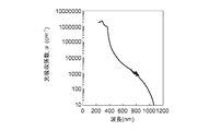
図1は、シリコンを媒質とする光の吸収係数を示したもので、波長が1,100nm近傍の近赤外光の光吸収係数は小さく検出感度は低い。そのため、従来は何らかの工夫をシリコンの光センサに施すことにより近赤外光に対する感度を向上させていた。
その工夫の一つとして、光センサに入射する近赤外光を光センサ内で分散させることで近赤外光が、光センサ内を通過する光路長を延ばして感度を向上させることが特許文献1や非特許文献1に記載されている。具体的には、受光素子が形成されるシリコンの表面にピラミッド状の凹凸を形成することによりこれを実現していた。FIG. 1 shows the absorption coefficient of light using silicon as a medium, and the light absorption coefficient of near-infrared light having a wavelength near 1,100 nm is small and the detection sensitivity is low. Therefore, conventionally, the sensitivity to near-infrared light has been improved by applying some ingenuity to the silicon optical sensor.
As one of the ingenuity, it is a patent document that the near-infrared light incident on the optical sensor is dispersed in the optical sensor to extend the optical path length of the near-infrared light passing through the optical sensor and improve the sensitivity. 1 and Non-Patent
さらに、デフューザと呼ばれる特別な層を受光素子表面に形成することにより近赤外光を分散させ感度の向上を図っていた。しかし、これらの従来の方法は製造プロセスの増加を招き、コストの上昇を伴う。また近赤外光の分散だけでは十分な感度の改善につながらず限界があった。
これに対し、光電変換領域となる空乏層を厚くする方法は感度向上には有効である。Furthermore, by forming a special layer called a diffuser on the surface of the light receiving element, near-infrared light is dispersed and the sensitivity is improved. However, these conventional methods lead to an increase in the manufacturing process and an increase in cost. In addition, the dispersion of near-infrared light alone did not lead to a sufficient improvement in sensitivity, and there was a limit.
On the other hand, the method of thickening the depletion layer serving as the photoelectric conversion region is effective for improving the sensitivity.
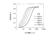
図2は各光波長に対して、空乏層幅と光吸収率との関係を示したものである。この図によれば、空乏層幅を300μm以上に制御出来れば近赤外領域にある光に対して十分な光吸収が得られることが分かる。 FIG. 2 shows the relationship between the depletion layer width and the light absorption rate for each light wavelength. According to this figure, it can be seen that if the depletion layer width can be controlled to 300 μm or more, sufficient light absorption can be obtained for light in the near infrared region.
図3は、pn接合が形成されるシリコン基板の不純物濃度に対する、逆方向バイアス電圧と空乏層幅との関係を示したものである。
一般に使用されているシリコン基板の濃度は1×10¹⁵/cm3程度であるが、低濃度基板(〜1×1012/cm3)を用いると空乏層幅は同一バイアス電圧で約一桁厚くなることが分かる。FIG. 3 shows the relationship between the reverse bias voltage and the depletion layer width with respect to the impurity concentration of the silicon substrate on which the pn junction is formed.
The density of a generally used silicon substrate is about 1 × 10 15 / cm 3 , but when a low concentration substrate (~ 1 × 10 12 / cm 3 ) is used, the depletion layer width is about an order of magnitude thicker at the same bias voltage. It turns out to be.
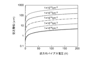
図4は、光波長をパラメータとして、可視光と同程度の感度を持つための逆方向バイアス電圧と基板の不純物濃度との関係を示したものである。
基板濃度が2×10¹²/cm3程度のFZ基板を使用して、波長940nmの近赤外光に対し、可視光と同程度の感度を持つ光センサを実現するには、50V程度のバイアス電圧を印加する必要があることが分かる。
このため、光センサはpn接合ダイオードに逆方向バイアス電圧を印加するための高電圧を発生させる高電圧発生回路を備えている。高電圧発生回路は、通常、電源電圧(VCC)を昇圧して所定の高電圧を得るための回路で、チャージポンプ回路が知られている。FIG. 4 shows the relationship between the reverse bias voltage for having the same sensitivity as visible light and the impurity concentration of the substrate with the light wavelength as a parameter.
In order to realize an optical sensor having the same sensitivity as visible light with respect to near-infrared light having a wavelength of 940 nm using an FZ substrate having a substrate concentration of about 2 × 10 12 / cm 3, a bias of about 50 V is used. It turns out that it is necessary to apply a voltage.
Therefore, the optical sensor includes a high voltage generation circuit that generates a high voltage for applying a reverse bias voltage to the pn junction diode. The high voltage generation circuit is usually a circuit for boosting the power supply voltage (VCC) to obtain a predetermined high voltage, and a charge pump circuit is known.
チャージポンプ回路は、コンデンサ(C1〜C9)とダイオード(D1〜D9)とを用いて入力信号(電源電圧:VCC)をオン・オフに切り替えることにより実現させる回路で、種々の回路構成が知られており、図5にその一例を示す。
このチャージポンプ回路をシリコン基板に形成すると、その占有面積が増大し、光センサが大型化するという欠点がある。The charge pump circuit is a circuit realized by switching the input signal (power supply voltage: VCS) on and off using a capacitor (C1 to C9) and a diode (D1 to D9), and various circuit configurations are known. An example is shown in FIG.
If this charge pump circuit is formed on a silicon substrate, the occupied area is increased, and the optical sensor has a drawback that the size is increased.
そこで、チャージポンプ回路を特許文献2に示すように、シリコン基板と該シリコン基板上に形成された絶縁膜と該絶縁膜上に形成された半導体層とを備えたSOI基板の該半導体層中に形成することも知られている。この文献に開示されているチャージポンプ回路では該半導体層中に形成されたp型領域とn型領域とを接合して互いに独立した複数のダイオードを形成し、そのダイオードを直列接続している。
Therefore, as shown in
本発明は、シリコン基板に形成される受光素子となるpn接合ダイオードに高電圧の逆方向バイアス電圧を印加したときに十分に厚い(広い)空乏層を得ることが出来、かつ高電圧発生回路による占有面積の増大を招かない半導体イメージセンサを実現することを目的とする。 According to the present invention, a sufficiently thick (wide) depletion layer can be obtained when a high voltage reverse bias voltage is applied to a pn junction diode, which is a light receiving element formed on a silicon substrate, and a high voltage generation circuit is used. The purpose is to realize a semiconductor image sensor that does not increase the occupied area.
本発明の半導体イメージセンサは、シリコン基板と該シリコン基板上に形成された絶縁膜と該絶縁膜上に形成された半導体層とを備えたSOI基板の前記絶縁膜下の前記シリコン基板に形成されると共に、前記シリコン基板の主面に垂直な方向に形成され近赤外光に感度を有するpn接合ダイオードからなる受光素子と、前記pn接合ダイオードに逆方向バイアス電圧を印加するための印加電圧を発生させる高電圧発生回路とを備え、前記シリコン基板の不純物濃度が1×10¹²/cm3乃至1×1014/cm3の範囲にあり、膜厚が300μm乃至700μmの範囲にあり、前記印加電圧が10V乃至60Vの範囲にあることを特徴とする。The semiconductor image sensor of the present invention is formed on the silicon substrate under the insulating film of the SOI substrate including the silicon substrate, the insulating film formed on the silicon substrate, and the semiconductor layer formed on the insulating film. In addition, a light receiving element made of a pn junction diode formed in a direction perpendicular to the main surface of the silicon substrate and having sensitivity to near-infrared light, and an applied voltage for applying a reverse bias voltage to the pn junction diode are used. A high voltage generating circuit for generating is provided, the impurity concentration of the silicon substrate is in the range of 1 × 10 12 /
また本発明の半導体イメージセンサは、前記絶縁膜を介して、前記半導体層を第1電極とし、前記シリコン基板に形成された拡散層を第2電極とするBOXキャパシタを含み、前記第1電極は前記高電圧発生回路の出力端に接続されることを特徴とする。 Further, the semiconductor image sensor of the present invention includes a BOX capacitor having the semiconductor layer as a first electrode and a diffusion layer formed on the silicon substrate as a second electrode via the insulating film, and the first electrode is It is characterized in that it is connected to the output terminal of the high voltage generation circuit.
また本発明の半導体イメージセンサは、前記BOXキャパシタの前記絶縁膜の膜厚が100nm乃至300nmの範囲にあることを特徴とする。 Further, the semiconductor image sensor of the present invention is characterized in that the film thickness of the insulating film of the BOX capacitor is in the range of 100 nm to 300 nm.
本発明の半導体イメージセンサは、前記絶縁膜上の前記半導体層に形成され、チャンネル領域をはさんで互いに接する第1領域と第2領域と、前記チャンネル領域上に形成されたゲート電極とを備え、前記第1領域と前記チャンネル領域とは互いに同一の導電型を有し、前記第2領域と前記チャンネル領域とは互いに異なる導電型を有し、前記ゲート電極と前記第2領域とを接続して、前記チャンネル領域を介した前記第1領域と前記第2領域とをダイオードとして用い、かつ複数個の前記ダイオードを直列接続し、それぞれのダイオードに信号を与え高電圧を出力するチャージポンプ回路を前記高電圧発生回路とすることを特徴とする。 The semiconductor image sensor of the present invention includes a first region and a second region formed on the semiconductor layer on the insulating film and in contact with each other across the channel region, and a gate electrode formed on the channel region. The first region and the channel region have the same conductive type, the second region and the channel region have different conductive types, and the gate electrode and the second region are connected to each other. A charge pump circuit that uses the first region and the second region via the channel region as diodes, connects a plurality of the diodes in series, gives a signal to each diode, and outputs a high voltage. The high voltage generating circuit is used.
さらに本発明の半導体イメージセンサは、前記半導体層の不純物濃度が1×10¹⁵/cm3乃至3×1018/cm3の範囲にあり、前記半導体層の膜厚が10nm乃至100nmの範囲にあることを特徴とする。Further, in the semiconductor image sensor of the present invention, the impurity concentration of the semiconductor layer is in the range of 1 × 10 15 /
低不純物濃度のSOI基板を用い、SOI基板の半導体層にチャージポンプ回路からなる高電圧発生回路を形成し、基板内に近赤外光に感度を有するpn接合ダイオードからなる受光素子を形成することにより、単一電源でプロセスや面積の増加も抑制された高感度の近赤外センサを実現することができる。 Using an SOI substrate with a low impurity concentration, a high voltage generation circuit consisting of a charge pump circuit is formed on the semiconductor layer of the SOI substrate, and a light receiving element composed of a pn junction diode having sensitivity to near-infrared light is formed in the substrate. As a result, it is possible to realize a highly sensitive near-infrared sensor in which the increase in process and area is suppressed with a single power supply.
以下、図面を参照して本発明の実施の形態の一例を詳細に説明する。 Hereinafter, an example of the embodiment of the present invention will be described in detail with reference to the drawings.
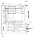
(第1の実施の形態)
図6は、本発明の第1の実施の形態に係る光センサの構成を示す概略平面図、図7は図6のA−A’断面を模式的に示すA−A’断面概略図である。
本発明に係る光センサ1000は、センサ回路部100と高電圧発生回路部200と制御回路部300とから構成される。
センサ回路部100は、受光素子100aと受光素子100aに流れる光電流を検出するMOSトランジスタ110aとから構成されている。受光素子100aはpn接合ダイオードからなる複数の単センサピクセルPをアレイ状に配列してセンサ回路部100が構成されている。受光素子100aは、図7に示すように低濃度N型シリコン基板101の裏面に形成されたN+拡散層103をカソード電極とし、この低濃度N型シリコン基板101主面近傍に形成されたP+拡散層105をアノード電極としている。(First Embodiment)
FIG. 6 is a schematic plan view showing the configuration of the optical sensor according to the first embodiment of the present invention, and FIG. 7 is a schematic cross-sectional view taken along the line AA'of FIG. ..
The
The
このように受光素子100aは、シリコン基板101と該シリコン基板上に形成された埋込酸化膜(BOX)102と該BOX102上に形成された半導体層(SOI層)107とを備えたSOI基板のBOX102下のシリコン基板101の主面に垂直な方向に形成され、波長800nm乃至1000nm程度の近赤外光に十分な感度を有するようシリコン基板101の不純物濃度と、その膜厚が選択される。光電流を検出するMOSトランジスタ110aはSOI層107に形成され図8に示すような周知のLDD構造のMOSFETである。
As described above, the
シリコン基板101の不純物濃度としては1×10¹²/cm3乃至1×1014/cm3の範囲で、好ましくは2×1012/cm3に選択する。シリコン基板101の厚さは受光素子100aが完全空乏化できるシリコン厚、例えば最終ウェハ厚300μm乃至700μm、好ましくは500μmとなるように選択する。裏面のシリコンをエッチング除去し、その後裏面にリン(P)をイオン注入し、活性化のため裏面からレーザ照射(レーザアニール)することにより裏面にN+層103を形成する。
このN+層103は空乏層が主面から伸びて、裏面最下部まで到着しないようにするためと、ピクセルアレイ全体で裏面抵抗を十分に下げるために形成される。The impurity concentration of the
The N + layer 103 is formed to prevent the depletion layer from extending from the main surface and reaching the bottom of the back surface, and to sufficiently reduce the back surface resistance of the entire pixel array.
制御回路部300は、センサ回路部100を制御するもので、垂直シフトレジスタ310、ノイズキャンセラ320、カラムADC330、水平シフトレジスタ340で構成され、センサ回路部の周辺に配置されている。
なお、制御回路部300は、本発明とは直接の関連性はないので、その構成や構造については説明を省略する。The
Since the
高電圧発生回路部200は、一例として、図5に示すキャパシタ(C1〜C9)とダイオード(D1〜D9)とを用いたチャージポンプ回路として構成される。なお、図7には、図5に示すチャージポンプ回路の一部が示されており、SOI層107に形成され、ダイオード接続されている2つのMOSトランジスタ110b,110cは、それぞれ図5に示すダイオードD8,D9に対応する。
As an example, the high voltage
また、MIMキャパシタ111はキャパシタC8に、BOXキャパシタ112はキャパシタC9にそれぞれ対応する。図5に示す他のダイオード(D1〜D7)やキャパシタ(C1〜C7)については図示は省略されている。ダイオード接続されて構成されている2つのMOSトランジスタ110b,110cの構造はMOSトランジスタ110aと同様に図8に示す周知のLDD構造のMOSFETである。
Further, the
図5に示す高電圧発生回路部200で発生した高電圧VO(5)は、図示しないメタル配線層を介してセンサ回路部100の周辺に設けたシリコン基板101の下層のN+層103に供給され、シリコン基板101全体が高電圧に保たれ、受光素子部100a内のP+拡散層105からシリコン基板101の裏面に向かって十分な厚さの空乏層がシリコン基板101内に形成される。The high voltage VO (5) generated in the high voltage
キャパシタ111(C8)は、絶縁層となるSiON膜をCVD法により下層のアルミニウム配線109a上に堆積し、その後、その上にTiNを堆積させてパターニングして対抗電極109bとするMIMキャパシタとして形成される。キャパシタ112(C9)は、高電圧発生回路200の出力端(Output)に接続されるもので耐圧を大きくとるために埋込酸化膜(BOX)102を絶縁層として用い、一方の電極をSOI層107に、他方の電極をシリコン基板101内のPウェル層106に形成されたP+拡散層105とするもので、BOXの膜厚を100nm乃至300nmに選択しておけば、50V以上の十分に高い耐圧を有する。The capacitor 111 (C8) is formed as a MIM capacitor in which a SiON film to be an insulating layer is deposited on the
図5では、一例として5段のチャージポンプ回路が示されており、入力クロックのハイ(High)レベル(Vcc)の5倍のDC電圧が出力されることになる。
入力が電源電圧VCCのクロック信号であると、N段のチャージポンプ回路では、その出力電圧は、
Vout(N)=VCC×N−Vf×2(N−1) ・・・(1)
となる。ここでVfはダイオード接続されたMOSFETの閾値電圧である。
このように適当な段数のチャージポンプ回路を準備することで、所望の高電圧(例えば10V乃至60V)を電源電圧VCCから発生させることができる。In FIG. 5, a five-stage charge pump circuit is shown as an example, and a DC voltage five times the high level (Vcc) of the input clock is output.
When the input is a clock signal of the power supply voltage VCS, in the N-stage charge pump circuit, the output voltage is
Vout (N) = VCS x N-Vf x 2 (N-1) ... (1)
Will be. Here, Vf is the threshold voltage of the diode-connected MOSFET.
By preparing a charge pump circuit having an appropriate number of stages in this way, a desired high voltage (for example, 10V to 60V) can be generated from the power supply voltage VCS.
図5に示す回路において、各段の電位差Vdiffは、
Vdiff=Vcc−2Vf ・・・(2)
となるため、各ダイオードD1〜D9の両端子間には、VCC以下の電圧しか印加されない。
しかし、通常のLSIのようにバルク(シリコン基板)にMOSFETを形成した場合には、後段のダイオード接続されたFETのドレイン接合部には高電圧(例えば30V)が図9に示すようにそのまま印加されてしまう(なお、ゲート(G)とソース(S)間には閾値電圧(1.8V)が印加される。)ため、pn接合部がこの高電圧に耐え得るように接合を傾斜化させて電界を緩和するなどの措置を必要とし、追加のプロセスが必要となり複雑化し、またMOSFETの面積の増大化を招いていた。In the circuit shown in FIG. 5, the potential difference Vdiff of each stage is
Vdiff = Vcc-2Vf ... (2)
Therefore, only a voltage of VCS or less is applied between both terminals of the diodes D1 to D9.
However, when a MOSFET is formed on a bulk (silicon substrate) like a normal LSI, a high voltage (for example, 30 V) is applied as it is to the drain junction of the diode-connected FET in the subsequent stage as shown in FIG. (Note that a threshold voltage (1.8V) is applied between the gate (G) and the source (S)), so the junction is tilted so that the pn junction can withstand this high voltage. Therefore, measures such as mitigating the electric field were required, additional processes were required, complicated, and the area of the MOSFET was increased.
これに対し、本発明では、ダイオードとなるMOSFETが図10に示すように埋込酸化膜(BOX)上の半導体層に互いに分離されて形成されているため、各段のダイオードが完全に分離され、電源電圧VCCに耐えるだけの耐圧があれば足り、高電圧発生回路であっても通常の電源電圧VCCで動作可能なMOSFETを使用することができる。
またキャパシタC1〜C8にもVCC以下の電圧しか印加されないので、図7に示すようなMIMキャパシタ111を用いることができる。
ただし、出力電圧安定用のキャパシタC9にはそのまま高電圧が印加されるため、キャパシタに耐圧確保が必要となる。本発明においては、100〜300nmの厚さのBOX102を使用して十分な耐圧を確保している。On the other hand, in the present invention, since the MOSFETs to be the diodes are formed separately from each other in the semiconductor layer on the embedded oxide film (BOX) as shown in FIG. 10, the diodes in each stage are completely separated. It is sufficient that the withstand voltage is sufficient to withstand the power supply voltage VCS, and even a high voltage generating circuit can use a MOSFET that can operate at a normal power supply voltage VCS.
Further, since only the voltage of VCS or less is applied to the capacitors C1 to C8, the
However, since a high voltage is applied to the capacitor C9 for stabilizing the output voltage as it is, it is necessary to secure a withstand voltage for the capacitor. In the present invention, a
なお、図7に示す高電圧発生回路部200では、出力される高電圧は、受光素子100aのpn接合キャパシタの片方の端子(N+層103)に接続されていることからキャパシタC9は省略することも可能である。
このように、低不純物濃度のSOI基板と、SOI基板の半導体層にチャージポンプ回路を構成する高電圧発生回路を組み合わせることで、単一電源でプロセスや面積の増加も抑制された高感度の近赤外センサを作製することができる。In the high voltage
In this way, by combining the SOI substrate with low impurity concentration and the high voltage generation circuit that constitutes the charge pump circuit on the semiconductor layer of the SOI substrate, the increase in process and area is suppressed with a single power supply. An infrared sensor can be manufactured.
次に図11〜図17を参照して本発明の光センサ1000の第1の実施の形態に係る高電圧発生回路部200の製造工程を説明する。
まず図11(A)に示すように、出発材料(Starting material)として不純物濃度が1×10¹²/cm3乃至1×1014/cm3の範囲にあるN型リンドープされた低濃度シリコン基板501上に100nm乃至300nmの埋込酸化膜(BOX)502、その上に膜厚が10nm乃至100nmの範囲にある不純物濃度が約1×1015/cm3のボロンドープされた薄いシリコン層(SOI層)503を備えたシリコン基板を準備する。
このような仕様のシリコン基板は公知のスマートカット法や張り合わせ法によって製造され、ウェハベンダより供給されている。Next, the manufacturing process of the high voltage
First, as shown in FIG. 11 (A), as a starting material, an N-type phosphorus-doped low-
Silicon substrates with such specifications are manufactured by known smart cutting methods and laminating methods, and are supplied by wafer vendors.
次に、図11(B)に示すようにレジストを用いたホトリソグラフィとそのレジストをマスクとしたシリコン(Si)のドライエッチングによりSOI層503をパターニングし、アクティブ領域を形成する。
なお、図中、左側にNチャネルMOSFETが、右側にPチャネルMOSFETが形成されるものとする。Next, as shown in FIG. 11B, the
In the figure, it is assumed that the N-channel MOSFET is formed on the left side and the P-channel MOSFET is formed on the right side.
次に、図11(C)に示すように素子分離を行う。周知の素子分離技術であるSTI(Shallow Trench Isolation)を用いて、アクティブなSOI層503間を素子分離酸化膜504で埋め込む。
次に、図11(D)に示すように、ホトリソグラフィとレジストをマスクとしたイオン注入技術を用いて、NチャネルMOSFET側のSOI層503aの上層にボロン(BF2 +)、PチャネルMOSFET側のSOI層503bの上層にリン(P+)をドープし、それぞれ所望の閾値となるように所望のドーズ・エネルギでイオン注入を行う。Next, element separation is performed as shown in FIG. 11 (C). Using STI (Shallow Trench Isolation), which is a well-known device separation technique, the active SOI layers 503 are embedded with the device
Next, as shown in FIG. 11 (D), using an ion implantation technique as a mask photolithography and photoresist, boron (BF 2 +) in the upper layer of the
次に、図12(E)に示すように、ホトリソグラフィにより作成したレジストパターン505をマスクとして、ボロン(B+)を下層のシリコン基板501に注入し、低濃度のPwell層506を形成する。この時上層にあるSOI層503a,503bにはわずかなボロンしか注入されないため、その不純物濃度はほとんど変化しない。レジストパターン505はイオン注入後除去される。
次に、図12(F)に示すように、熱酸化により、SOI層503a,503bの上層にゲート酸化膜(シリコン酸化膜)507を形成する。Next, as shown in FIG. 12 (E), boron (B + ) is injected into the
Next, as shown in FIG. 12 (F), a gate oxide film (silicon oxide film) 507 is formed on the upper layers of the SOI layers 503a and 503b by thermal oxidation.
次に図12(G)に示すように、ゲート電極となるポリシリコンをCVD(Chemical Vapor Deposition)により表面全面に堆積させ、ホトリソグラフィとレジストをマスクとするドライエッチングにより、ポリシリコンからなるゲート電極508を形成する。
次に図12(H)に示すように、下層のシリコン基板501とのコンタクトを形成するために、コンタクト部にある素子分離酸化膜504と埋込酸化膜502とをホトリソグラフィとレジストをマスクとしたドライエッチングにより除去し、BOXウインドを形成する。Next, as shown in FIG. 12 (G), polysilicon as a gate electrode is deposited on the entire surface by CVD (Chemical Vapor Deposition), and a gate electrode made of polysilicon is subjected to photolithography and dry etching using a resist as a mask.
Next, as shown in FIG. 12 (H), in order to form a contact with the
次に、図13(I)に示すように、通常のホトリソグラフィとレジストをマスクとしたボロン(B+)のイオン注入により、センスノードとなるP+層509を形成する。レジストはイオン注入後除去する。
次に図13(J)に示すように、ホトリソグラフィとゲート電極508をマスクとしたイオン注入により、NチャネルMOSFET側には、ヒ素(As)を注入したソース・ドレインn+層510をPチャネルMOSFET側には、ボロン(BF2)を注入したソース・ドレインp+層511を形成する。なおゲート電極508にサイドウォール(SW)を周知の方法で形成することで、ソース・ドレインn+層の内側にn−層をソース・ドレインp+層の内側にp−層を形成し、LDDタイプのMOSFETとすることが出来る。
センスノードp+層509を含めたこれらの拡散層(ソース・ドレインn+層510およびソース・ドレインp+層511)での不純物の活性化のため高温(1,000℃程度)で、10秒程度の熱処理(アニール)をチッ素(N2)雰囲気中で行う。Next, as shown in FIG. 13 (I), a P +
Next, as shown in FIG. 13 (J), the source / drain n +
10 seconds at high temperature (about 1,000 ° C) for activation of impurities in these diffusion layers (source drain n + layer 510 and source drain p + layer 511) including the sense node p + layer 509. A degree of heat treatment (annealing) is performed in a nitrogen (N 2 ) atmosphere.
次に図13(K)に示すように、層間絶縁(シリコン酸化膜)512をCVDにより全面に堆積させ、表面平坦化のために化学機械研磨(CMP)を行う。
その後図13(L)に示すように、ホトリソグラフィとレジストをマスクとするドライエッチングにより層間絶縁膜に素子間の電気的接続用のコンタクトホールを形成する。Next, as shown in FIG. 13 (K), the interlayer insulation (silicon oxide film) 512 is deposited on the entire surface by CVD, and chemical mechanical polishing (CMP) is performed for surface flattening.
After that, as shown in FIG. 13 (L), a contact hole for electrical connection between the elements is formed in the interlayer insulating film by photolithography and dry etching using a resist as a mask.
次に、図14(M)に示すように、コンタクト内を導電物で埋め込むため、図示しないバリアメタル(Ti/TiN),タングステン(W)をCVDにより埋積させ、その後CMPにより層間絶縁膜512上部のW及びTi/TiNを除去し、MIタングステンプラグ513を形成する。
次に図14(N)に示すように、Ti/TiN/Al−Cu/Ti/TiNを順次スパッタし、ホトリソグラフィとレジストをマスクとしたドライエッチングにより、M1配線514を形成する。この後、図示しない、絶縁膜の堆積、平坦化(CMP)、ビアホール形成、プラグ埋込、配線層の形成パターニングを繰り返すことにより、層間絶縁膜512の上層に複数のM1配線514を形成することが出来る。Next, as shown in FIG. 14 (M), in order to embed the inside of the contact with a conductive material, barrier metals (Ti / TiN) and tungsten (W) (not shown) are embedded by CVD, and then the
Next, as shown in FIG. 14 (N), Ti / TiN / Al—Cu / Ti / TiN are sequentially sputtered, and
次に、図15(O)に示すように、M2タングステンプラグ516に接続された2層目のM2配線517上にMIMキャパシタを形成する場合、M2配線517のパターニング後、キャパシタの絶縁膜となるSiON膜をCVDによりM2配線517上に堆積し、その後、キャパシタの対抗電極となるTiNからなるMIM電極519をスパッタし、パターニングすることにより、MIMキャパシタが形成される。
Next, as shown in FIG. 15 (O), when a MIM capacitor is formed on the second
次に、図16(P)に示すように、全面にM2−M3層絶縁膜520を堆積し、コンタクトホール内にM3タングステンプラグをスパッタし、図14(N)、図15(O)で説明したと同様のプロセスを繰返して、M3配線522を形成し、パッシベーション523に所望の開口を設けてボンディングパッドを形成することにより表面処理を完了する。
Next, as shown in FIG. 16 (P), an M2-M3
最後に、センサが完全空乏化できるように最終ウェハ厚を300μm乃至700μmとなるように、シリコン基板501の裏面をグラインドし、ウェットエッチングによりダメージ層を除去する。その後、裏面にリンをイオン注入し、活性化のため、裏面からレーザアニールで行って、その後シリコン基板501の裏面にn+層524を形成する。
なお第1の実施の形態においては、高電圧発生回路200で使用されるダイオード(D1〜D9)は、図13(J)で形成された、NチャネルMOSFETを図10に示すように、ドレイン(D)とゲート(G)とを接続して使用している。Finally, the back surface of the
In the first embodiment, the diodes (D1 to D9) used in the high
本発明の第2の実施の形態では、図18に示すように、埋込酸化膜(BOX)502上の半導体層であるSOI層603にチャンネル領域603aをはさんで互いに接する第1領域603bと第2領域603cとを形成し、チャンネル領域603a上にゲート酸化膜607を介して形成されたゲート電極608を備え、第1領域603bとチャンネル領域603aとは互いに同一の導電型を有し、第2領域603cとチャンネル領域603aとは互いに異なる導電型を有し、ゲート電極608と第2領域603cとを接続して、チャンネル領域603aを介した第1領域603bと第2領域603cをダイオード(D1〜D9)として使用している。
In the second embodiment of the present invention, as shown in FIG. 18, the
図18に示すようなダイオードは図10に示すSOI−MOSFETの構造とほぼ同等であり、図11乃至図17で説明したプロセスフロー自体はほとんど変わらない。
即ち、図11(D)において、SOI層503a,503bの両方にリン(P+)をドーピングし、図13(J)において右側のPチャネルMOSFETのソース(S)をp+/p−層からn+/n−層に変更しただけであり、ソース及びドレインへのイオン注入時にゲート508の真ん中でレジストをマスクにして図19に示すようにヒ素(As+)とボロン(BF2 +)とを打ち分ければ図18に示すようなダイオードを作製することができる。The diode as shown in FIG. 18 has almost the same structure as the SOI-MOSFET shown in FIG. 10, and the process flow itself described in FIGS. 11 to 17 is almost the same.
That is, in FIG. 11 (D), both the SOI layers 503a and 503b are implanted with phosphorus (P + ), and in FIG. 13 (J), the source (S) of the right P-channel MOSFET is transferred from the p + / p − layer. n + / n - it is only changed in the layer, and the resist in the middle of the
図20は図7に示すような受光素子100aに裏面から光照射したときの光波長に対する量子効率を測定した結果を示す図である。なおpn接合に印加した逆バイアス電圧は30Vである。
非特許文献1に示されるセンサと比較して、本発明に係るセンサは900nm〜1,000nmの光波長の近赤外光に対してかなり高い量子効率が得られることが分かる。FIG. 20 is a diagram showing the results of measuring the quantum efficiency with respect to the light wavelength when the
It can be seen that the sensor according to the present invention can obtain considerably higher quantum efficiency with respect to near-infrared light having an optical wavelength of 900 nm to 1,000 nm as compared with the sensor shown in
次にチャージポンプ内のSOI構造で使用される3種類のダイオードについて、逆方向バイアス時のリーク電流について考察する。
リーク電流が増加すると、チャージポンプ回路の昇圧効果が悪くなり、所望の電圧に昇圧するためのダイオードとキャパシタとのセットの段数を増やさねばならず、面積が大きくなるという不具合につながるからである。Next, the leakage current at the time of reverse bias will be considered for the three types of diodes used in the SOI structure in the charge pump.
This is because when the leakage current increases, the boosting effect of the charge pump circuit deteriorates, and the number of stages of the set of the diode and the capacitor for boosting to a desired voltage must be increased, which leads to a problem that the area becomes large.
図21は3種類のダイオードの構造を比較して示したもので、(A)は特許文献2に記載されたダイオード、(B)はMOSFETをダイオード接続して構成されるもので、本発明の第1の実施の形態で使用されているもの(図10参照)、(C)は本発明の第2の実施の形態で使用されているもの(図18参照)である。
21A and 21B show a comparison of the structures of three types of diodes. FIG. 21A is a diode described in
(A)に示す構造のダイオードは、構造及びプロセス上、矢線で示す面がプロセスダメージを受け易く、また表面準位を低減するための酸化も出来ない。そのため界面準位が多く、逆バイアス時には空乏層がこの界面と接触するため、界面準位を介した表面再結合電流が流れ、リーク電流が増加するという欠点がある。
(B)に示す構造のダイオードは、チャネル領域上にゲート酸化膜が形成されているため、表面準位は(A)のものに比較して少ない。しかし、所謂、GIDL(Gate Induced Drain Leakage)によって逆バイアス時のリーク電流が増加するという欠点がある。
(C)に示す構造のダイオードは、SOIのシリコン表面と酸化膜の界面で空乏層ができるところはゲート酸化膜のところであるため、良好な界面であり、界面準位は少ないため、準位を介するリーク電流は抑えられる。
逆バイアスが印加されているときn+/n−/n部分でのGIDL発生の可能性はあるが、n+/n−/nの構造となっているため、空乏層が横方向に広がり易くなり横方向電界を十分に緩和できる。従ってGIDLの発生量は十分に抑えられる。Due to the structure and process of the diode having the structure shown in (A), the surface indicated by the arrow line is susceptible to process damage, and the diode cannot be oxidized to reduce the surface level. Therefore, there are many interface states, and the depletion layer comes into contact with this interface during reverse bias, so that a surface recombination current flows through the interface state, resulting in an increase in leakage current.
Since the gate oxide film is formed on the channel region of the diode having the structure shown in (B), the surface level is smaller than that of (A). However, there is a drawback that the leakage current at the time of reverse bias increases due to so-called GIDL (Gate Induced Drain Leakage).
The diode having the structure shown in (C) has a good interface because the depletion layer is formed at the interface between the silicon surface of SOI and the oxide film at the gate oxide film, and the interface state is small. Leakage current through is suppressed.
When a reverse bias is applied, there is a possibility that GIDL will occur at the n + / n − / n portion, but the structure of n + / n − / n makes it easy for the depletion layer to spread in the lateral direction. The lateral electric field can be sufficiently relaxed. Therefore, the amount of GIDL generated is sufficiently suppressed.
図22は、図21に示した3つのダイオード構造における逆方向バイアス電圧とリーク電流との関係を示した図である。
逆バイアス電圧を−1.8Vとし、図21(C)に示すダイオードを使用することで、リーク電流は、測定限界以下となり、図21(A)に示すダイオードに比して、約2桁以上リーク電流を低減することが出来る。FIG. 22 is a diagram showing the relationship between the reverse bias voltage and the leakage current in the three diode structures shown in FIG. 21.
By setting the reverse bias voltage to -1.8V and using the diode shown in FIG. 21 (C), the leakage current is below the measurement limit, which is about two orders of magnitude or more compared to the diode shown in FIG. 21 (A). Leakage current can be reduced.
501 低濃度シリコン基板
502 埋込酸化膜
503 SOI層
504 素子分離酸化膜
505 レジストパターン
506 Pwell層
507 ゲート酸化膜
508 ゲート電極
509 センスノードp+層
510 ソース・ドレインn+層
511 ソース・ドレインp+層
512 層間絶縁膜
513 M1タングステンプラグ
514 M1配線
515 M1−M2層間絶縁膜
516 M2タングステンプラグ
517 M2配線
518 MIM絶縁膜
519 MIM電極
520 M2−M3層間絶縁膜
521 M3タングステンプラグ
522 M3配線
523 パッシベーション
524 裏面n+層501 Low-
Claims (4)
前記pn接合ダイオードに逆方向バイアス電圧を印加するための印加電圧を発生させる高電圧発生回路と、
前記絶縁膜を介して、前記半導体層を第1電極とし、前記シリコン基板に形成された拡散層を第2電極とするBOXキャパシタとを含み、
前記第1電極は前記高電圧発生回路の出力端に接続され、
前記シリコン基板の不純物濃度が1×10¹²/cm3乃至1×1014/cm3の範囲にあり、膜厚が300μm乃至700μmの範囲にあり、前記印加電圧が10V乃至60Vの範囲にあることを特徴とする半導体イメージセンサ。 A silicon substrate, an insulating film formed on the silicon substrate, and a semiconductor layer formed on the insulating film are formed on the silicon substrate under the insulating film of the SOI substrate, and the main silicon substrate is formed. A light receiving element made of a pn junction diode formed in a direction perpendicular to the surface and having sensitivity to near-infrared light,
A high voltage generation circuit that generates an applied voltage for applying a reverse bias voltage to the pn junction diode, and
A BOX capacitor having the semiconductor layer as the first electrode and the diffusion layer formed on the silicon substrate as the second electrode via the insulating film is included.
The first electrode is connected to the output end of the high voltage generation circuit.
The impurity concentration of the silicon substrate is in the range of 1 × 10 12 / cm 3 to 1 × 10 14 / cm 3 , the film thickness is in the range of 300 μm to 700 μm, and the applied voltage is in the range of 10 V to 60 V. A semiconductor image sensor characterized by.
前記第2領域と前記チャンネル領域とは互いに異なる導電型を有し、
前記ゲート電極と前記第2領域とを接続して、前記チャンネル領域を介した前記第1領域と前記第2領域とをダイオードとして用い、かつ複数個の前記ダイオードを直列接続し、それぞれのダイオードに信号を与え高電圧を出力するチャージポンプ回路を前記高電圧発生回路とすることを特徴とする請求項1又は2に記載の半導体イメージセンサ。 The first region includes a first region and a second region formed on the semiconductor layer on the insulating film and in contact with the channel region across the channel region, and a gate electrode formed on the channel region. And the channel region have the same conductive type as each other,
The second region and the channel region have different conductive types and have different conductive types.
The gate electrode and the second region are connected, the first region and the second region via the channel region are used as diodes, and a plurality of the diodes are connected in series to each diode. The semiconductor image sensor according to claim 1 or 2, wherein the charge pump circuit that gives a signal and outputs a high voltage is the high voltage generating circuit.
Applications Claiming Priority (1)
| Application Number | Priority Date | Filing Date | Title |
|---|---|---|---|
| PCT/JP2020/016184 WO2021205662A1 (en) | 2020-04-10 | 2020-04-10 | Semiconductor image sensor |
Publications (3)
| Publication Number | Publication Date |
|---|---|
| JP6873336B1 true JP6873336B1 (en) | 2021-05-19 |
| JPWO2021205662A1 JPWO2021205662A1 (en) | 2021-10-14 |
| JPWO2021205662A5 JPWO2021205662A5 (en) | 2022-03-14 |
Family
ID=75896357
Family Applications (1)
| Application Number | Title | Priority Date | Filing Date |
|---|---|---|---|
| JP2020545811A Active JP6873336B1 (en) | 2020-04-10 | 2020-04-10 | Semiconductor image sensor |
Country Status (6)
| Country | Link |
|---|---|
| US (1) | US20220199661A1 (en) |
| EP (1) | EP4135038A4 (en) |
| JP (1) | JP6873336B1 (en) |
| CN (1) | CN113785396B (en) |
| TW (1) | TWI757098B (en) |
| WO (1) | WO2021205662A1 (en) |
Families Citing this family (2)
| Publication number | Priority date | Publication date | Assignee | Title |
|---|---|---|---|---|
| WO2023190406A1 (en) * | 2022-03-29 | 2023-10-05 | ラピスセミコンダクタ株式会社 | Semiconductor device and solid-state imaging device |
| WO2023190407A1 (en) * | 2022-03-29 | 2023-10-05 | ラピスセミコンダクタ株式会社 | Semiconductor device and solid-state imaging device |
Citations (18)
| Publication number | Priority date | Publication date | Assignee | Title |
|---|---|---|---|---|
| JPS5754370A (en) * | 1980-09-19 | 1982-03-31 | Nippon Telegr & Teleph Corp <Ntt> | Insulating gate type transistor |
| JPS5895877A (en) * | 1981-12-01 | 1983-06-07 | Semiconductor Res Found | Semiconductor photoelectric transducer device |
| JPH01276766A (en) * | 1988-04-28 | 1989-11-07 | Seiko Epson Corp | Thin film diode and static electricity protection circuit using same |
| WO1995026573A1 (en) * | 1994-03-28 | 1995-10-05 | Seiko Instruments Inc. | Semiconductor device for detecting light and radiation, and method of manufacturing the device |
| JP2001503918A (en) * | 1996-11-01 | 2001-03-21 | ローレンス バークレイ ラボラトリー | Low resistivity photon transmissive window mounted on a photosensitive silicon detector |
| JP2003520441A (en) * | 2000-01-11 | 2003-07-02 | コーニンクレッカ フィリップス エレクトロニクス エヌ ヴィ | Charge pump circuit |
| JP2004134672A (en) * | 2002-10-11 | 2004-04-30 | Sony Corp | Method and apparatus for manufacturing super-thin semiconductor device and super-thin backlighting type solid-state imaging device |
| JP2005340479A (en) * | 2004-05-26 | 2005-12-08 | Nippon Telegr & Teleph Corp <Ntt> | Semiconductor device and manufacturing method thereof |
| JP2006509358A (en) * | 2002-12-09 | 2006-03-16 | クォンタム セミコンダクター リミテッド ライアビリティ カンパニー | CMOS image sensor |
| JP2010041010A (en) * | 2008-08-08 | 2010-02-18 | Oki Semiconductor Co Ltd | Light sensor |
| JP2012080045A (en) * | 2010-10-06 | 2012-04-19 | Lapis Semiconductor Co Ltd | Semiconductor device |
| US20130075593A1 (en) * | 2004-11-19 | 2013-03-28 | Voxtel, Inc. | Active pixel sensors with variable threshold reset |
| WO2013129559A1 (en) * | 2012-02-29 | 2013-09-06 | Etoh Takeharu | Solid-state imaging device |
| JP2014093616A (en) * | 2012-11-02 | 2014-05-19 | High Energy Accelerator Research Organization | Digital tdi system detector |
| JP2014130920A (en) * | 2012-12-28 | 2014-07-10 | Lapis Semiconductor Co Ltd | Double-well structure soi radiation sensor and method of manufacturing the same |
| JP2014130890A (en) * | 2012-12-28 | 2014-07-10 | Canon Inc | Photoelectric conversion device |
| JP2014135454A (en) * | 2013-01-11 | 2014-07-24 | Lapis Semiconductor Co Ltd | Semiconductor device and manufacturing method of the same |
| JP2014232761A (en) * | 2013-05-28 | 2014-12-11 | キヤノン株式会社 | Solid-state imaging device |
Family Cites Families (9)
| Publication number | Priority date | Publication date | Assignee | Title |
|---|---|---|---|---|
| JP3285443B2 (en) | 1993-12-22 | 2002-05-27 | 三菱電機株式会社 | Charge pump |
| JP2006005294A (en) * | 2004-06-21 | 2006-01-05 | Renesas Technology Corp | Semiconductor apparatus |
| CN102859693B (en) * | 2010-04-16 | 2015-12-16 | 夏普株式会社 | Semiconductor device |
| EP2980841B1 (en) * | 2013-03-25 | 2020-05-27 | Renesas Electronics Corporation | Semiconductor device and method for manufacturing same |
| JP2017108062A (en) | 2015-12-11 | 2017-06-15 | ソニー株式会社 | Solid state imaging device, imaging apparatus, and method of manufacturing solid state imaging device |
| EP3516692B1 (en) * | 2016-09-23 | 2022-02-16 | Apple Inc. | Stacked backside illuminated spad array |
| US10312275B2 (en) * | 2017-04-25 | 2019-06-04 | Semiconductor Components Industries, Llc | Single-photon avalanche diode image sensor with photon counting and time-of-flight detection capabilities |
| US10636930B2 (en) * | 2017-09-29 | 2020-04-28 | Taiwan Semiconductor Manufacturing Company Ltd. | SPAD image sensor and associated fabricating method |
| US11462538B2 (en) * | 2017-12-06 | 2022-10-04 | Semiconductor Energy Laboratory Co., Ltd. | Semiconductor device |
-
2020
- 2020-04-10 CN CN202080028666.1A patent/CN113785396B/en active Active
- 2020-04-10 WO PCT/JP2020/016184 patent/WO2021205662A1/en unknown
- 2020-04-10 EP EP20919389.5A patent/EP4135038A4/en active Pending
- 2020-04-10 US US17/603,572 patent/US20220199661A1/en active Pending
- 2020-04-10 JP JP2020545811A patent/JP6873336B1/en active Active
-
2021
- 2021-02-19 TW TW110105596A patent/TWI757098B/en active
Patent Citations (18)
| Publication number | Priority date | Publication date | Assignee | Title |
|---|---|---|---|---|
| JPS5754370A (en) * | 1980-09-19 | 1982-03-31 | Nippon Telegr & Teleph Corp <Ntt> | Insulating gate type transistor |
| JPS5895877A (en) * | 1981-12-01 | 1983-06-07 | Semiconductor Res Found | Semiconductor photoelectric transducer device |
| JPH01276766A (en) * | 1988-04-28 | 1989-11-07 | Seiko Epson Corp | Thin film diode and static electricity protection circuit using same |
| WO1995026573A1 (en) * | 1994-03-28 | 1995-10-05 | Seiko Instruments Inc. | Semiconductor device for detecting light and radiation, and method of manufacturing the device |
| JP2001503918A (en) * | 1996-11-01 | 2001-03-21 | ローレンス バークレイ ラボラトリー | Low resistivity photon transmissive window mounted on a photosensitive silicon detector |
| JP2003520441A (en) * | 2000-01-11 | 2003-07-02 | コーニンクレッカ フィリップス エレクトロニクス エヌ ヴィ | Charge pump circuit |
| JP2004134672A (en) * | 2002-10-11 | 2004-04-30 | Sony Corp | Method and apparatus for manufacturing super-thin semiconductor device and super-thin backlighting type solid-state imaging device |
| JP2006509358A (en) * | 2002-12-09 | 2006-03-16 | クォンタム セミコンダクター リミテッド ライアビリティ カンパニー | CMOS image sensor |
| JP2005340479A (en) * | 2004-05-26 | 2005-12-08 | Nippon Telegr & Teleph Corp <Ntt> | Semiconductor device and manufacturing method thereof |
| US20130075593A1 (en) * | 2004-11-19 | 2013-03-28 | Voxtel, Inc. | Active pixel sensors with variable threshold reset |
| JP2010041010A (en) * | 2008-08-08 | 2010-02-18 | Oki Semiconductor Co Ltd | Light sensor |
| JP2012080045A (en) * | 2010-10-06 | 2012-04-19 | Lapis Semiconductor Co Ltd | Semiconductor device |
| WO2013129559A1 (en) * | 2012-02-29 | 2013-09-06 | Etoh Takeharu | Solid-state imaging device |
| JP2014093616A (en) * | 2012-11-02 | 2014-05-19 | High Energy Accelerator Research Organization | Digital tdi system detector |
| JP2014130920A (en) * | 2012-12-28 | 2014-07-10 | Lapis Semiconductor Co Ltd | Double-well structure soi radiation sensor and method of manufacturing the same |
| JP2014130890A (en) * | 2012-12-28 | 2014-07-10 | Canon Inc | Photoelectric conversion device |
| JP2014135454A (en) * | 2013-01-11 | 2014-07-24 | Lapis Semiconductor Co Ltd | Semiconductor device and manufacturing method of the same |
| JP2014232761A (en) * | 2013-05-28 | 2014-12-11 | キヤノン株式会社 | Solid-state imaging device |
Also Published As
| Publication number | Publication date |
|---|---|
| US20220199661A1 (en) | 2022-06-23 |
| WO2021205662A1 (en) | 2021-10-14 |
| CN113785396A (en) | 2021-12-10 |
| CN113785396B (en) | 2022-05-10 |
| EP4135038A4 (en) | 2024-02-21 |
| EP4135038A1 (en) | 2023-02-15 |
| JPWO2021205662A1 (en) | 2021-10-14 |
| TWI757098B (en) | 2022-03-01 |
| TW202141775A (en) | 2021-11-01 |
Similar Documents
| Publication | Publication Date | Title |
|---|---|---|
| US7274394B2 (en) | Solid state image pickup device and manufacturing method therefor | |
| US6429487B1 (en) | Semiconductor device having gate to body connection | |
| US6512280B2 (en) | Integrated CMOS structure for gate-controlled buried photodiode | |
| US8344468B2 (en) | Photovoltaic device with lateral P-I-N light-sensitive diodes | |
| JP6213006B2 (en) | Semiconductor device | |
| JP6873336B1 (en) | Semiconductor image sensor | |
| US6392263B1 (en) | Integrated structure for reduced leakage and improved fill-factor in CMOS pixel | |
| JP2003264311A (en) | Method for making integrated circuit having photodiode | |
| JP3212150B2 (en) | Semiconductor device | |
| US8232586B2 (en) | Silicon photon detector | |
| US6707126B2 (en) | Semiconductor device including a PIN photodiode integrated with a MOS transistor | |
| US6452212B1 (en) | Semiconductor device and method for operating the same | |
| US10593724B2 (en) | Method of manufacturing a semiconductor device | |
| JP2003264243A (en) | Integrated circuit including two types of photodiodes | |
| US6753202B2 (en) | CMOS photodiode having reduced dark current and improved light sensitivity and responsivity | |
| US20030197228A1 (en) | CMOS image sensor and method of fabricating the same | |
| Goiffon et al. | Ionizing radiation effects on CMOS imagers manufactured in deep submicron process | |
| WO2023233833A1 (en) | Semiconductor image sensor device | |
| JP3975391B2 (en) | Semiconductor device, image sensor, PIN diode, and electronic device | |
| KR20000041462A (en) | Fabrication method of image sensor having pinned photodiode | |
| JPS62141758A (en) | Semiconductor storage device | |
| JPS62208674A (en) | Semiconductor device | |
| JPS6051081A (en) | Semiconductor image pickup device | |
| JPH05343625A (en) | Semiconductor device |
Legal Events
| Date | Code | Title | Description |
|---|---|---|---|
| A521 | Request for written amendment filed |
Free format text: JAPANESE INTERMEDIATE CODE: A523 Effective date: 20200901 |
|
| A621 | Written request for application examination |
Free format text: JAPANESE INTERMEDIATE CODE: A621 Effective date: 20200901 |
|
| A871 | Explanation of circumstances concerning accelerated examination |
Free format text: JAPANESE INTERMEDIATE CODE: A871 Effective date: 20200901 |
|
| A521 | Request for written amendment filed |
Free format text: JAPANESE INTERMEDIATE CODE: A523 Effective date: 20201007 |
|
| A975 | Report on accelerated examination |
Free format text: JAPANESE INTERMEDIATE CODE: A971005 Effective date: 20201215 |
|
| A131 | Notification of reasons for refusal |
Free format text: JAPANESE INTERMEDIATE CODE: A131 Effective date: 20210112 |
|
| A521 | Request for written amendment filed |
Free format text: JAPANESE INTERMEDIATE CODE: A523 Effective date: 20210114 |
|
| TRDD | Decision of grant or rejection written | ||
| A01 | Written decision to grant a patent or to grant a registration (utility model) |
Free format text: JAPANESE INTERMEDIATE CODE: A01 Effective date: 20210413 |
|
| A61 | First payment of annual fees (during grant procedure) |
Free format text: JAPANESE INTERMEDIATE CODE: A61 Effective date: 20210420 |
|
| R150 | Certificate of patent or registration of utility model |
Ref document number: 6873336 Country of ref document: JP Free format text: JAPANESE INTERMEDIATE CODE: R150 |
|
| R250 | Receipt of annual fees |
Free format text: JAPANESE INTERMEDIATE CODE: R250 |